Embed Size (px)
Citation preview
OBSOLETE
LM4832
www.ti.com SNAS003E –FEBRUARY 1998–REVISED APRIL 2013
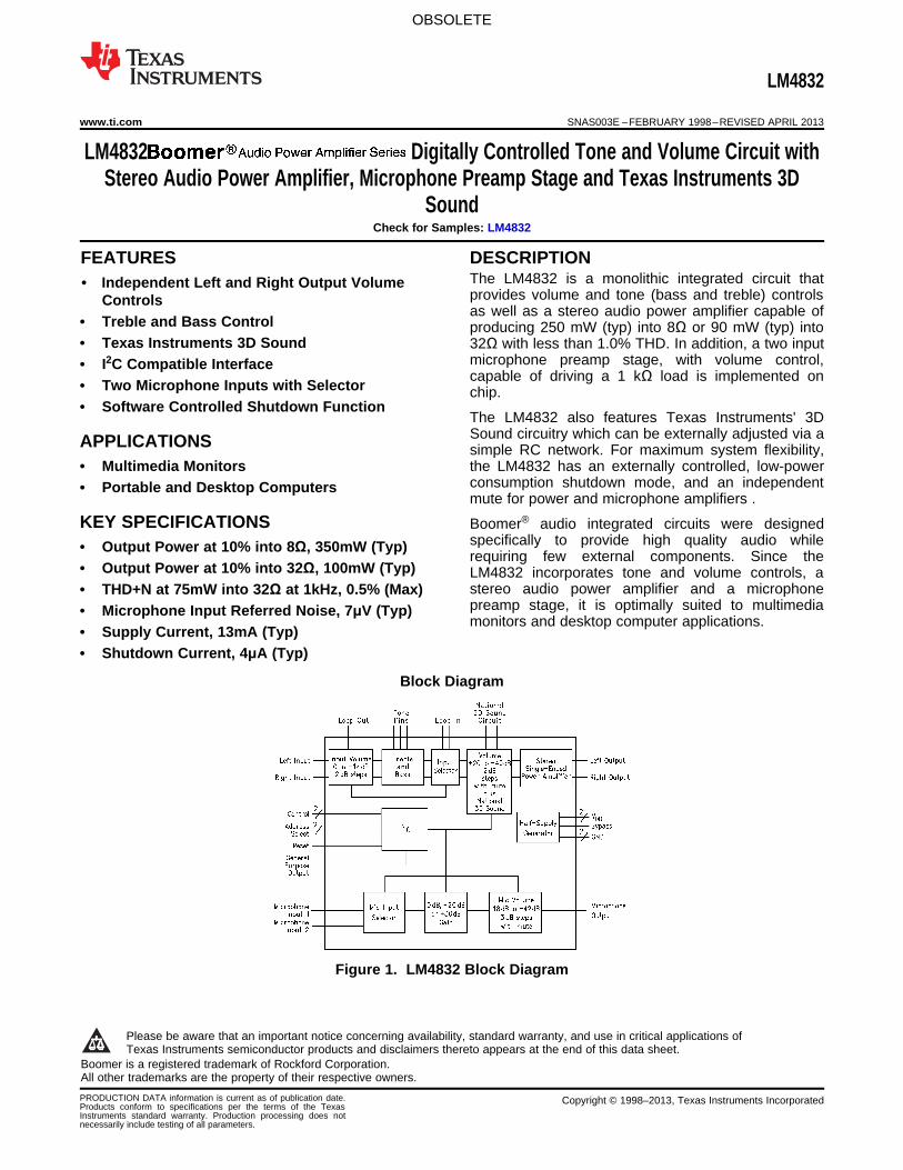
LM4832 Digitally Controlled Tone and Volume Circuit withStereo Audio Power Amplifier, Microphone Preamp Stage and Texas Instruments 3D
SoundCheck for Samples: LM4832
1FEATURES DESCRIPTIONThe LM4832 is a monolithic integrated circuit that
23• Independent Left and Right Output Volumeprovides volume and tone (bass and treble) controlsControlsas well as a stereo audio power amplifier capable of
• Treble and Bass Control producing 250 mW (typ) into 8Ω or 90 mW (typ) into• Texas Instruments 3D Sound 32Ω with less than 1.0% THD. In addition, a two input
microphone preamp stage, with volume control,• I2C Compatible Interfacecapable of driving a 1 kΩ load is implemented on
• Two Microphone Inputs with Selector chip.• Software Controlled Shutdown Function
The LM4832 also features Texas Instruments' 3DSound circuitry which can be externally adjusted via aAPPLICATIONS simple RC network. For maximum system flexibility,
• Multimedia Monitors the LM4832 has an externally controlled, low-powerconsumption shutdown mode, and an independent• Portable and Desktop Computersmute for power and microphone amplifiers .
KEY SPECIFICATIONS Boomer® audio integrated circuits were designedspecifically to provide high quality audio while• Output Power at 10% into 8Ω, 350mW (Typ)requiring few external components. Since the
• Output Power at 10% into 32Ω, 100mW (Typ) LM4832 incorporates tone and volume controls, astereo audio power amplifier and a microphone• THD+N at 75mW into 32Ω at 1kHz, 0.5% (Max)preamp stage, it is optimally suited to multimedia• Microphone Input Referred Noise, 7μV (Typ)monitors and desktop computer applications.
• Supply Current, 13mA (Typ)• Shutdown Current, 4μA (Typ)
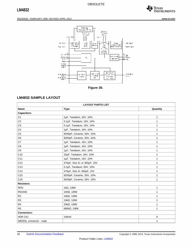
Block Diagram
Figure 1. LM4832 Block Diagram
1
Please be aware that an important notice concerning availability, standard warranty, and use in critical applications ofTexas Instruments semiconductor products and disclaimers thereto appears at the end of this data sheet.
2Boomer is a registered trademark of Rockford Corporation.3All other trademarks are the property of their respective owners.
PRODUCTION DATA information is current as of publication date. Copyright © 1998–2013, Texas Instruments IncorporatedProducts conform to specifications per the terms of the TexasInstruments standard warranty. Production processing does notnecessarily include testing of all parameters.
OBSOLETE
LM4832
SNAS003E –FEBRUARY 1998–REVISED APRIL 2013 www.ti.com
These devices have limited built-in ESD protection. The leads should be shorted together or the device placed in conductive foamduring storage or handling to prevent electrostatic damage to the MOS gates.
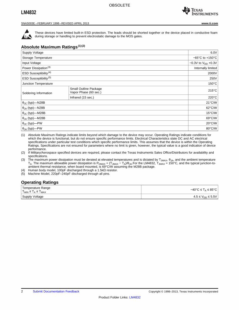
Absolute Maximum Ratings (1) (2)
Supply Voltage 6.0V
Storage Temperature −65°C to +150°C
Input Voltage −0.3V to VDD +0.3V
Power Dissipation (3) Internally limited
ESD Susceptibility (4) 2000V
ESD Susceptibility (5) 250V
Junction Temperature 150°C
Small Outline Package 215°CVapor Phase (60 sec.)Soldering InformationInfrared (15 sec.) 220°C
θJC (typ)—N28B 21°C/W
θJA (typ)—N28B 62°C/W
θJC (typ)—M28B 15°C/W
θJA (typ)—M28B 69°C/W
θJC (typ)—PW 20°C/W
θJA (typ)—PW 80°C/W
(1) Absolute Maximum Ratings indicate limits beyond which damage to the device may occur. Operating Ratings indicate conditions forwhich the device is functional, but do not ensure specific performance limits. Electrical Characteristics state DC and AC electricalspecifications under particular test conditions which specific performance limits. This assumes that the device is within the OperatingRatings. Specifications are not ensured for parameters where no limit is given, however, the typical value is a good indication of deviceperformance.
(2) If Military/Aerospace specified devices are required, please contact the Texas Instruments Sales Office/Distributors for availability andspecifications.
(3) The maximum power dissipation must be derated at elevated temperatures and is dictated by TJMAX, θJA, and the ambient temperatureTA. The maximum allowable power dissipation is PDMAX = (TJMAX − TA)/θJA.For the LM4832, TJMAX = 150°C, and the typical junction-to-ambient thermal resistance, when board mounted, is 69°C/W assuming the M28B package.
(4) Human body model, 100pF discharged through a 1.5kΩ resistor.(5) Machine Model, 220pF–240pF discharged through all pins.
Operating RatingsTemperature Range −40°C ≤ TA ≤ 85°CTMIN ≤ TA ≤ TMAX
Supply Voltage 4.5 ≤ VDD ≤ 5.5V
2 Submit Documentation Feedback Copyright © 1998–2013, Texas Instruments Incorporated
Product Folder Links: LM4832
OBSOLETE
LM4832
www.ti.com SNAS003E –FEBRUARY 1998–REVISED APRIL 2013
Electrical Characteristics for Entire IC (1)
The following specifications apply for VDD = 5V unless otherwise noted. Limits apply for TA = 25°C.
LM4832 UnitsSymbol Parameter Conditions (Limits)Typical (2) Limit (3) (4)
VDD Supply Voltage VIN = 0V, IO = 0A 4.5 V (min)
5.5 V (max)
IDD Quiescent Power Supply Current 13 21 mA (max)
ISD Shutdown Current 2.5 9 µA (max)
INPUT ATTENUATORS
AR Attenuator Range Attenuation at 0 dB Setting 1 dB (max)Attenuation at −14 dB Setting −15 dB (min)
AS Step Size 0 dB to −14 dB 2 dB
Gain Step Size Error 0.1 dB (max)
ET Channel to Channel Tracking Error 0.15 dB (max)
BASS CONTROL
AR Bass Control Range f = 100 Hz, VIN = 0.25V ±12 −14 dB (min)
14 dB (max)
AS Bass Step Size 2 dB
ESE Bass Step Size Error 0.5 dB (max)
ET Bass Tracking Error 0.15 dB (max)
TREBLE CONTROL
AR Treble Control Range fIN = 10 kHz, VIN = 0.25V ±12 −13 dB (min)
13 dB (max)
AS Treble Step Size 2 dB
ESE Treble Step Size Error 0.1 dB (max)
ET Treble Tracking Error 0.15 dB (max)
OUTPUT ATTENUATORS
AR Attenuator Range Gain at +20 dB Setting 21 dB (max)Attenuation at −40 dB Setting −42 dB (min)+20 dB to −40 dB
AS Step Size 2 dB
Step Size Error 0.1 dB (max)
ET Channel to Channel Tracking Error 0.1 dB (max)
AUDIO PATH
VOS Output Offset Voltage VIN = 0V 3 50 mV (max)
PO Output Power THD = 1.0% (max), f = 1 kHz, All controlsat 0dB
RL = 8Ω 250 mW (min)
RL = 32Ω 95 75 mW (min)
THD+N Total Harmonic Distortion+Noise All Controls at 0 dB, THD = 10%, f = 1 kHzRL = 8Ω 350 mW
PO = 200 mW, RL = 8Ω 0.15 %
PO = 75 mW, RL = 32Ω 0.11 %
VO = 1 Vrms, RL = 10Ω 0.08 %
PSRR Power Supply Rejection Ratio CB = 1 µF, f = 100 Hz, VRIPPLE = 100 45 dBmVrms, All Controls at 0 dB Setting
AM Mute Attenuation f = 1 kHz, VIN = 1V −75 dB
(1) All voltages are measured with respect to the ground pins, unless otherwise specified. All specifications are tested using the typicalapplications shown in Figure 1.
(2) Typicals are measured at 25°C and represent the parametric norm.(3) Limits are ensured AOQL (Average Outgoing Quality Level).(4) Data sheet min and max specification limits by design, test, or statistical analysis.
Copyright © 1998–2013, Texas Instruments Incorporated Submit Documentation Feedback 3
Product Folder Links: LM4832
OBSOLETE
LM4832
SNAS003E –FEBRUARY 1998–REVISED APRIL 2013 www.ti.com
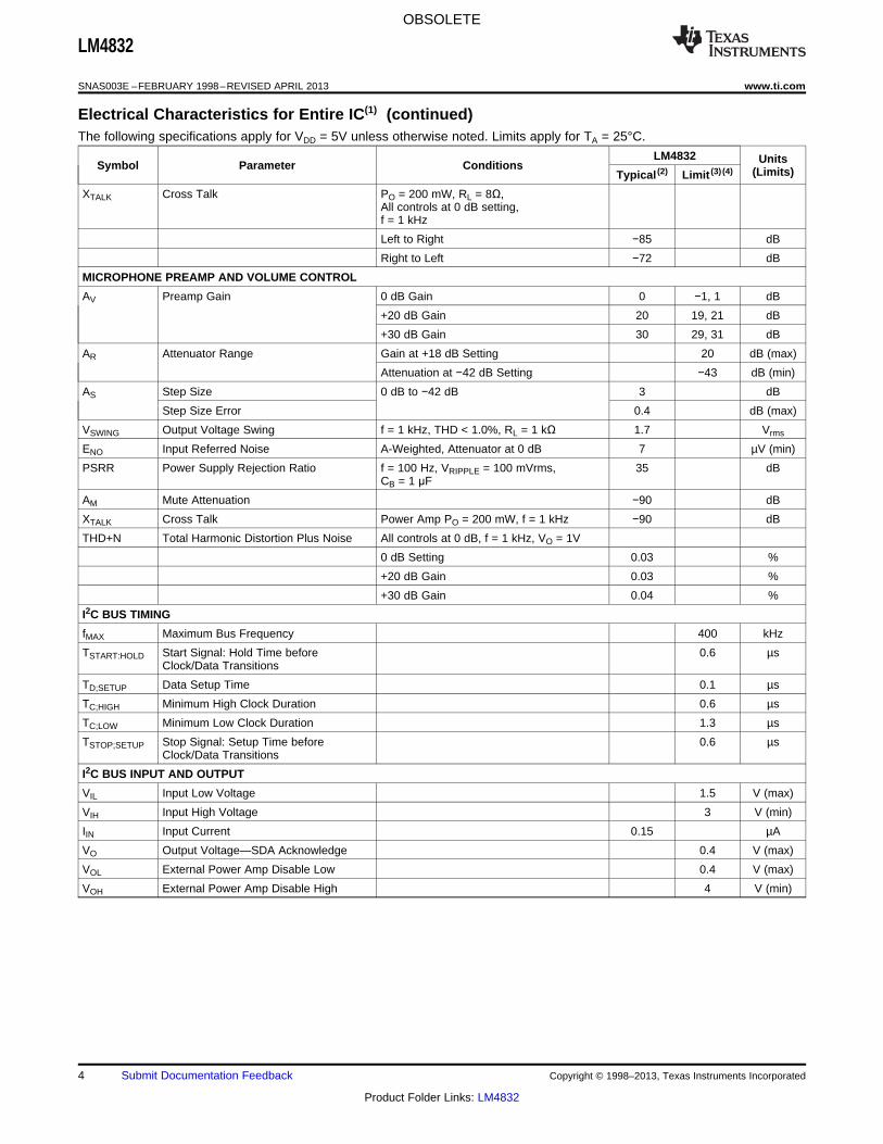
Electrical Characteristics for Entire IC(1) (continued)The following specifications apply for VDD = 5V unless otherwise noted. Limits apply for TA = 25°C.
LM4832 UnitsSymbol Parameter Conditions (Limits)Typical (2) Limit (3) (4)
XTALK Cross Talk PO = 200 mW, RL = 8Ω,All controls at 0 dB setting,f = 1 kHz
Left to Right −85 dB
Right to Left −72 dB
MICROPHONE PREAMP AND VOLUME CONTROL
AV Preamp Gain 0 dB Gain 0 −1, 1 dB
+20 dB Gain 20 19, 21 dB
+30 dB Gain 30 29, 31 dB
AR Attenuator Range Gain at +18 dB Setting 20 dB (max)
Attenuation at −42 dB Setting −43 dB (min)
AS Step Size 0 dB to −42 dB 3 dB
Step Size Error 0.4 dB (max)
VSWING Output Voltage Swing f = 1 kHz, THD < 1.0%, RL = 1 kΩ 1.7 Vrms
ENO Input Referred Noise A-Weighted, Attenuator at 0 dB 7 µV (min)
PSRR Power Supply Rejection Ratio f = 100 Hz, VRIPPLE = 100 mVrms, 35 dBCB = 1 μF
AM Mute Attenuation −90 dB
XTALK Cross Talk Power Amp PO = 200 mW, f = 1 kHz −90 dB
THD+N Total Harmonic Distortion Plus Noise All controls at 0 dB, f = 1 kHz, VO = 1V
0 dB Setting 0.03 %
+20 dB Gain 0.03 %
+30 dB Gain 0.04 %
I2C BUS TIMING
fMAX Maximum Bus Frequency 400 kHz
TSTART:HOLD Start Signal: Hold Time before 0.6 µsClock/Data Transitions
TD;SETUP Data Setup Time 0.1 µs
TC;HIGH Minimum High Clock Duration 0.6 µs
TC;LOW Minimum Low Clock Duration 1.3 µs
TSTOP;SETUP Stop Signal: Setup Time before 0.6 µsClock/Data Transitions
I2C BUS INPUT AND OUTPUT
VIL Input Low Voltage 1.5 V (max)
VIH Input High Voltage 3 V (min)
IIN Input Current 0.15 µA
VO Output Voltage—SDA Acknowledge 0.4 V (max)
VOL External Power Amp Disable Low 0.4 V (max)
VOH External Power Amp Disable High 4 V (min)
4 Submit Documentation Feedback Copyright © 1998–2013, Texas Instruments Incorporated
Product Folder Links: LM4832
OBSOLETE
LM4832
www.ti.com SNAS003E –FEBRUARY 1998–REVISED APRIL 2013
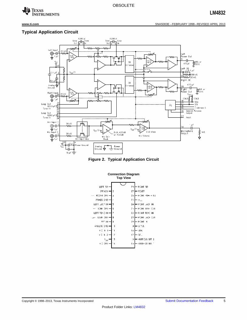
Typical Application Circuit
Figure 2. Typical Application Circuit
Connection DiagramTop View
Copyright © 1998–2013, Texas Instruments Incorporated Submit Documentation Feedback 5
Product Folder Links: LM4832
OBSOLETE
LM4832
SNAS003E –FEBRUARY 1998–REVISED APRIL 2013 www.ti.com
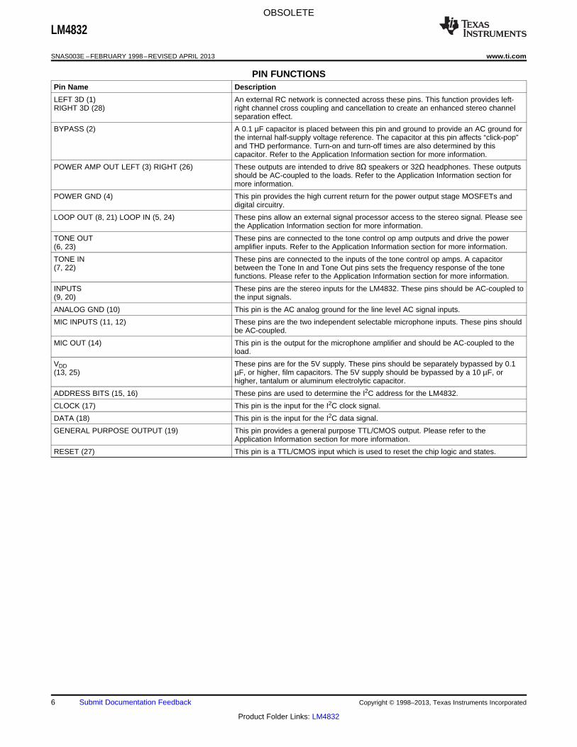
PIN FUNCTIONSPin Name Description
LEFT 3D (1) An external RC network is connected across these pins. This function provides left-RIGHT 3D (28) right channel cross coupling and cancellation to create an enhanced stereo channel
separation effect.
BYPASS (2) A 0.1 µF capacitor is placed between this pin and ground to provide an AC ground forthe internal half-supply voltage reference. The capacitor at this pin affects “click-pop”and THD performance. Turn-on and turn-off times are also determined by thiscapacitor. Refer to the Application Information section for more information.
POWER AMP OUT LEFT (3) RIGHT (26) These outputs are intended to drive 8Ω speakers or 32Ω headphones. These outputsshould be AC-coupled to the loads. Refer to the Application Information section formore information.
POWER GND (4) This pin provides the high current return for the power output stage MOSFETs anddigital circuitry.
LOOP OUT (8, 21) LOOP IN (5, 24) These pins allow an external signal processor access to the stereo signal. Please seethe Application Information section for more information.
TONE OUT These pins are connected to the tone control op amp outputs and drive the power(6, 23) amplifier inputs. Refer to the Application Information section for more information.
TONE IN These pins are connected to the inputs of the tone control op amps. A capacitor(7, 22) between the Tone In and Tone Out pins sets the frequency response of the tone
functions. Please refer to the Application Information section for more information.
INPUTS These pins are the stereo inputs for the LM4832. These pins should be AC-coupled to(9, 20) the input signals.
ANALOG GND (10) This pin is the AC analog ground for the line level AC signal inputs.
MIC INPUTS (11, 12) These pins are the two independent selectable microphone inputs. These pins shouldbe AC-coupled.
MIC OUT (14) This pin is the output for the microphone amplifier and should be AC-coupled to theload.
VDD These pins are for the 5V supply. These pins should be separately bypassed by 0.1(13, 25) µF, or higher, film capacitors. The 5V supply should be bypassed by a 10 µF, or
higher, tantalum or aluminum electrolytic capacitor.
ADDRESS BITS (15, 16) These pins are used to determine the I2C address for the LM4832.
CLOCK (17) This pin is the input for the I2C clock signal.
DATA (18) This pin is the input for the I2C data signal.
GENERAL PURPOSE OUTPUT (19) This pin provides a general purpose TTL/CMOS output. Please refer to theApplication Information section for more information.
RESET (27) This pin is a TTL/CMOS input which is used to reset the chip logic and states.
6 Submit Documentation Feedback Copyright © 1998–2013, Texas Instruments Incorporated
Product Folder Links: LM4832
OBSOLETE
LM4832
www.ti.com SNAS003E –FEBRUARY 1998–REVISED APRIL 2013
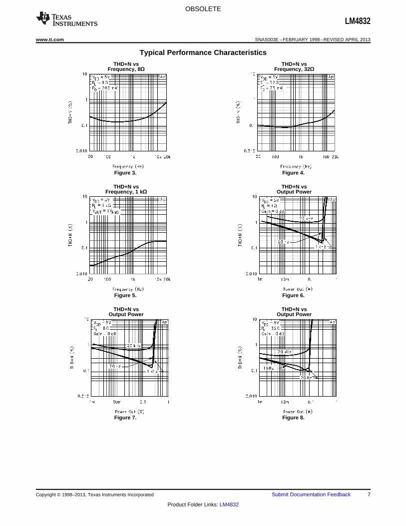
Typical Performance Characteristics
THD+N vs THD+N vsFrequency, 8Ω Frequency, 32Ω
Figure 3. Figure 4.
THD+N vs THD+N vsFrequency, 1 kΩ Output Power
Figure 5. Figure 6.
THD+N vs THD+N vsOutput Power Output Power
Figure 7. Figure 8.
Copyright © 1998–2013, Texas Instruments Incorporated Submit Documentation Feedback 7
Product Folder Links: LM4832
OBSOLETE
LM4832
SNAS003E –FEBRUARY 1998–REVISED APRIL 2013 www.ti.com
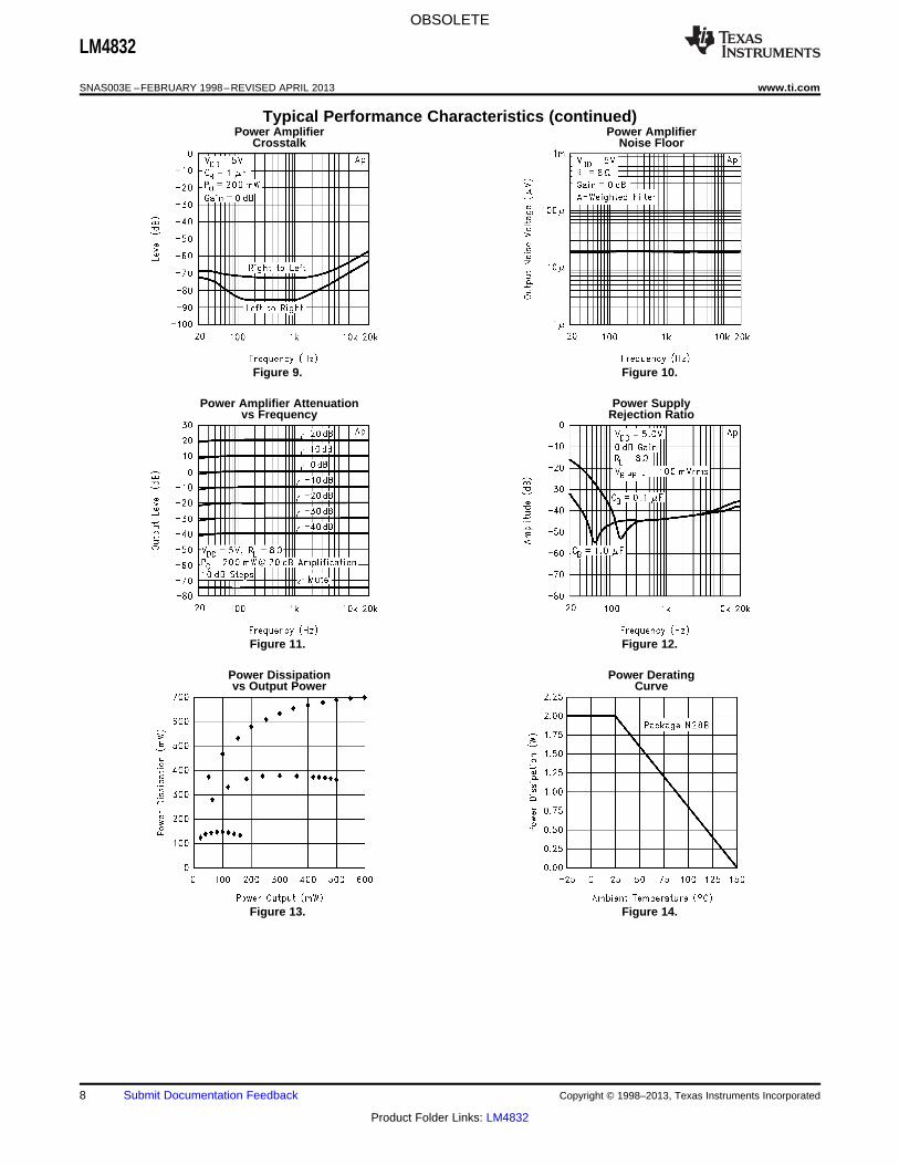
Typical Performance Characteristics (continued)Power Amplifier Power Amplifier
Crosstalk Noise Floor
Figure 9. Figure 10.
Power Amplifier Attenuation Power Supplyvs Frequency Rejection Ratio
Figure 11. Figure 12.
Power Dissipation Power Deratingvs Output Power Curve
Figure 13. Figure 14.
8 Submit Documentation Feedback Copyright © 1998–2013, Texas Instruments Incorporated
Product Folder Links: LM4832
OBSOLETE
LM4832
www.ti.com SNAS003E –FEBRUARY 1998–REVISED APRIL 2013
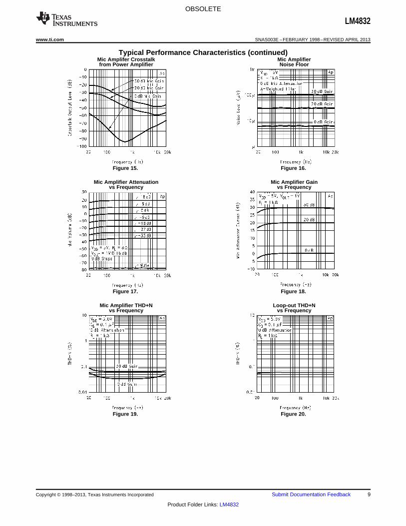
Typical Performance Characteristics (continued)Mic Amplifer Crosstalk Mic Amplifierfrom Power Amplifier Noise Floor
Figure 15. Figure 16.
Mic Amplifier Attenuation Mic Amplifier Gainvs Frequency vs Frequency
Figure 17. Figure 18.
Mic Amplifier THD+N Loop-out THD+Nvs Frequency vs Frequency
Figure 19. Figure 20.
Copyright © 1998–2013, Texas Instruments Incorporated Submit Documentation Feedback 9
Product Folder Links: LM4832
OBSOLETE
LM4832
SNAS003E –FEBRUARY 1998–REVISED APRIL 2013 www.ti.com
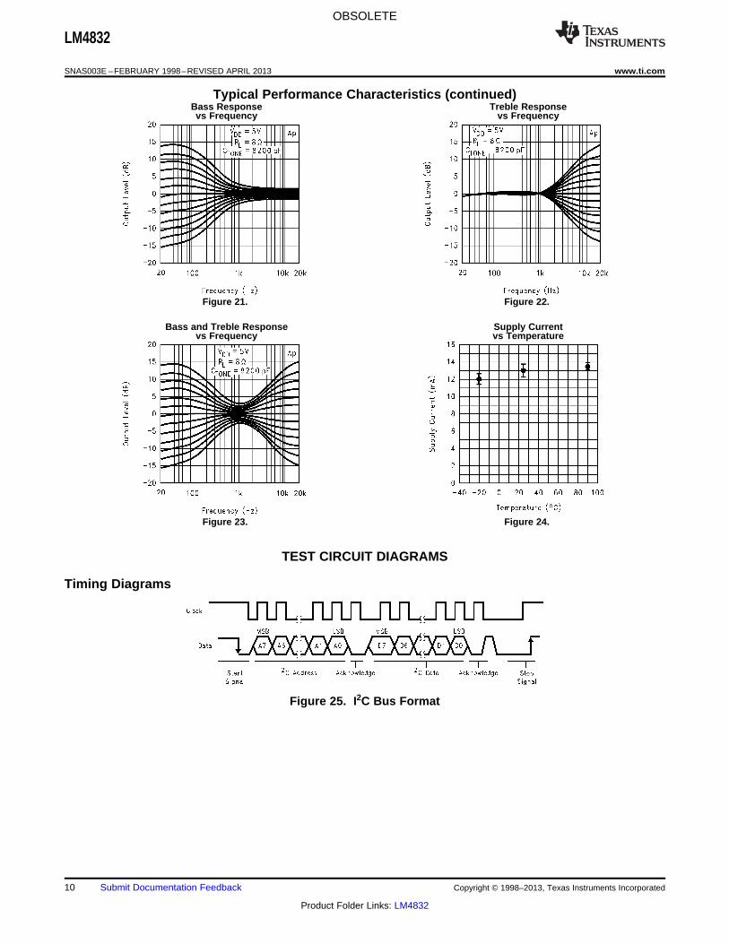
Typical Performance Characteristics (continued)Bass Response Treble Responsevs Frequency vs Frequency
Figure 21. Figure 22.
Bass and Treble Response Supply Currentvs Frequency vs Temperature
Figure 23. Figure 24.
TEST CIRCUIT DIAGRAMS
Timing Diagrams
Figure 25. I2C Bus Format
10 Submit Documentation Feedback Copyright © 1998–2013, Texas Instruments Incorporated
Product Folder Links: LM4832
OBSOLETE
LM4832
www.ti.com SNAS003E –FEBRUARY 1998–REVISED APRIL 2013
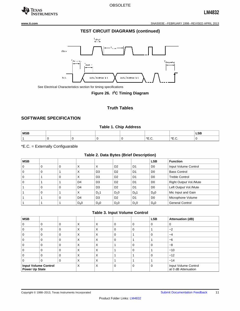
TEST CIRCUIT DIAGRAMS (continued)
See Electrical Characteristics section for timing specifications
Figure 26. I2C Timing Diagram
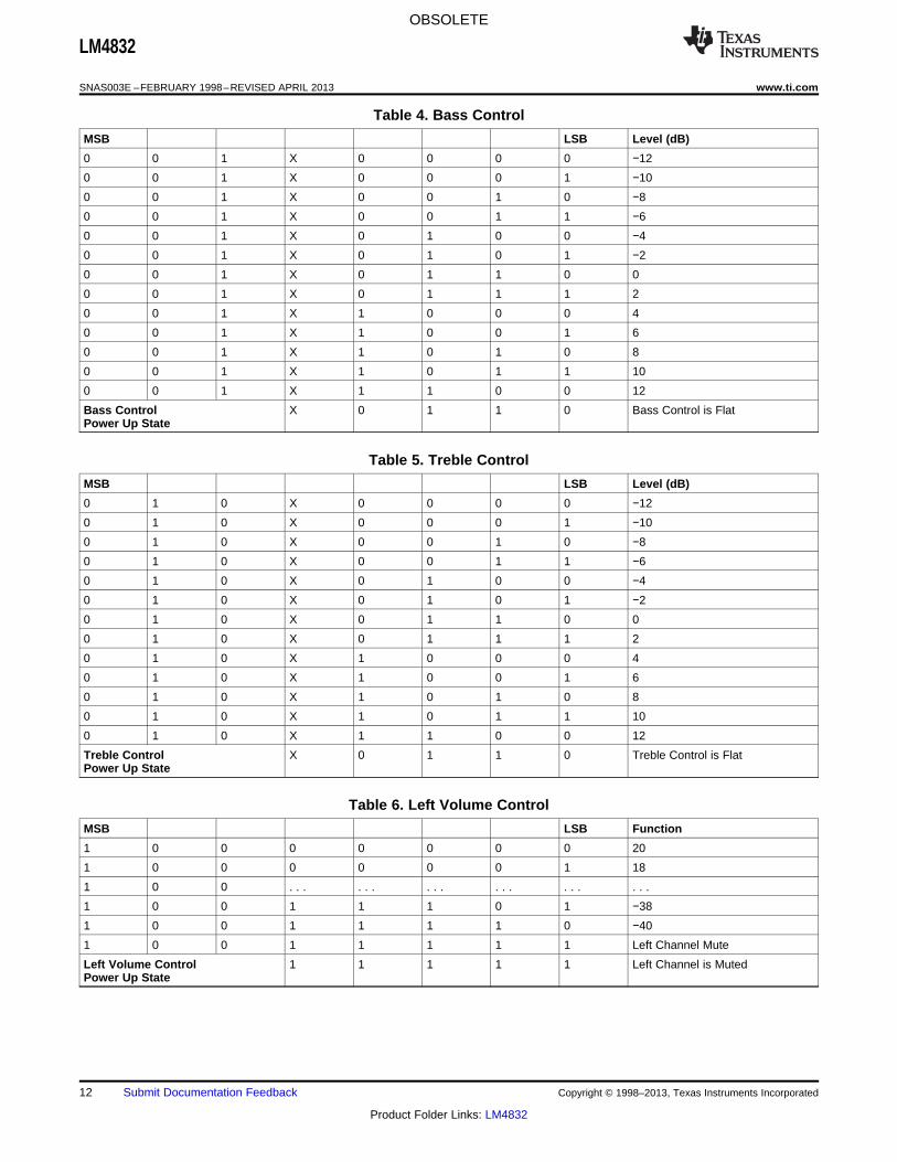
Truth Tables
SOFTWARE SPECIFICATION
Table 1. Chip Address
MSB LSB
1 0 0 0 0 *E.C. *E.C. 0
*E.C. = Externally Configuarable
Table 2. Data Bytes (Brief Description)
MSB LSB Function
0 0 0 X X D2 D1 D0 Input Volume Control
0 0 1 X D3 D2 D1 D0 Bass Control
0 1 0 X D3 D2 D1 D0 Treble Control
0 1 1 D4 D3 D2 D1 D0 Right Output Vol./Mute
1 0 0 D4 D3 D2 D1 D0 Left Output Vol./Mute
1 0 1 X D11 D10 D01 D00 Mic Input and Gain
1 1 0 D4 D3 D2 D1 D0 Microphone Volume
1 1 1 D40 D30 D20 D10 D00 General Control
Table 3. Input Volume Control
MSB LSB Attenuation (dB)
0 0 0 X X 0 0 0 0
0 0 0 X X 0 0 1 −2
0 0 0 X X 0 1 0 −4
0 0 0 X X 0 1 1 −6
0 0 0 X X 1 0 0 −8
0 0 0 X X 1 0 1 −10
0 0 0 X X 1 1 0 −12
0 0 0 X X 1 1 1 −14
Input Volume Control X X 0 0 0 Input Volume ControlPower Up State at 0 dB Attenuation
Copyright © 1998–2013, Texas Instruments Incorporated Submit Documentation Feedback 11
Product Folder Links: LM4832
OBSOLETE
LM4832
SNAS003E –FEBRUARY 1998–REVISED APRIL 2013 www.ti.com
Table 4. Bass Control
MSB LSB Level (dB)
0 0 1 X 0 0 0 0 −12
0 0 1 X 0 0 0 1 −10
0 0 1 X 0 0 1 0 −8
0 0 1 X 0 0 1 1 −6
0 0 1 X 0 1 0 0 −4
0 0 1 X 0 1 0 1 −2
0 0 1 X 0 1 1 0 0
0 0 1 X 0 1 1 1 2
0 0 1 X 1 0 0 0 4
0 0 1 X 1 0 0 1 6
0 0 1 X 1 0 1 0 8
0 0 1 X 1 0 1 1 10
0 0 1 X 1 1 0 0 12
Bass Control X 0 1 1 0 Bass Control is FlatPower Up State
Table 5. Treble Control
MSB LSB Level (dB)
0 1 0 X 0 0 0 0 −12
0 1 0 X 0 0 0 1 −10
0 1 0 X 0 0 1 0 −8
0 1 0 X 0 0 1 1 −6
0 1 0 X 0 1 0 0 −4
0 1 0 X 0 1 0 1 −2
0 1 0 X 0 1 1 0 0
0 1 0 X 0 1 1 1 2
0 1 0 X 1 0 0 0 4
0 1 0 X 1 0 0 1 6
0 1 0 X 1 0 1 0 8
0 1 0 X 1 0 1 1 10
0 1 0 X 1 1 0 0 12
Treble Control X 0 1 1 0 Treble Control is FlatPower Up State
Table 6. Left Volume Control
MSB LSB Function
1 0 0 0 0 0 0 0 20
1 0 0 0 0 0 0 1 18
1 0 0 . . . . . . . . . . . . . . . . . .
1 0 0 1 1 1 0 1 −38
1 0 0 1 1 1 1 0 −40
1 0 0 1 1 1 1 1 Left Channel Mute
Left Volume Control 1 1 1 1 1 Left Channel is MutedPower Up State
12 Submit Documentation Feedback Copyright © 1998–2013, Texas Instruments Incorporated
Product Folder Links: LM4832
OBSOLETE
LM4832
www.ti.com SNAS003E –FEBRUARY 1998–REVISED APRIL 2013
Table 7. General Control
MSB LSB Function
1 1 1 0 Chip On
1 1 1 1 Chip Shutdown
1 1 1 0 G.P.O. Output Low
1 1 1 1 G.P.O. Output High
1 1 1 0 Stereo Enhance Off
1 1 1 1 Stereo Enhance On
1 1 1 0 Stereo Operation
1 1 1 1 Mono Force On
1 1 1 0 External Loop Disable
1 1 1 1 External Loop Enable
General Control 0 0 0 0 0Power Up State
Table 8. Right Volume Control
MSB LSB Level (dB)
0 1 1 0 0 0 0 0 20
0 1 1 0 0 0 0 1 18
0 1 1 . . . . . . . . . . . . . . . . . .
0 1 1 1 1 1 0 0 −38
0 1 1 1 1 1 1 0 −40
0 1 1 1 1 1 1 1 Right Channel Mute
Right Volume Control 1 1 1 1 1 Right Channel Is MutedPower Up State
Table 9. Microphone Input Selection and Gain
MSB LSB Function
1 0 1 X 0 0 Mic Input 1
1 0 1 X 0 1 Mic Input 2
1 0 1 X 1 X Mic Input 1 and 2
1 0 1 X 0 0 Mic Gain (+0 dB)
1 0 1 X 0 1 Mic Gain (+20 dB)
1 0 1 X 1 0 Mic Gain (+30 dB)
Mic Input Sel. and X 1 0 0 0 Mic 1 is selectedGain Power Up State with a +30 dB gain
Table 10. Microphone Volume Control
MSB LSB Function
1 1 0 0 0 0 0 0 18
1 1 0 0 0 0 0 1 15
1 1 0 . . . . . . . . . . . . . . . . . .
1 1 0 1 0 1 0 0 −42
1 1 0 1 0 1 0 1 Microphone Muted
Mic Volume Control 1 0 1 0 1 Microphone MutedPower Up State
Copyright © 1998–2013, Texas Instruments Incorporated Submit Documentation Feedback 13
Product Folder Links: LM4832
OBSOLETE
LM4832
SNAS003E –FEBRUARY 1998–REVISED APRIL 2013 www.ti.com
APPLICATION INFORMATION
GROUNDING
In order to achieve the best possible performance, certain grounding techniques should be followed. All inputreference grounds should be tied with their respective source grounds and brought back to the power supplyground separately from the output load ground returns. These input grounds should also be tied in with the half-supply bypass ground. Bringing the ground returns for the output loads back to the supply separately will keeplarge signal currents from interfering with the stable AC input ground references.
LAYOUT
As stated in the Grounding section, placement of ground return lines is critical for maintaining the highest level ofsystem performance. It is not only important to route the correct ground return lines together, but also importantto be aware of where those ground return lines are routed in conjunction with each other. The output load groundreturns should be physically located as far as reasonably possible from low signal level lines and their groundreturn lines. Critical signal lines are those relating to the microphone amplifier section, since these lines generallywork at very low signal levels.
SUPPLY BYPASSING
As with all op amps and power op amps, the LM4832 requires the supplies to be bypassed to avoid oscillation.To avoid high frequency instabilities, a 0.1 µF metallized-film or ceramic capacitor should be used to bypass thesupplies as close to the chip as possible. For low frequency considerations, a 10 µF or greater tantalum orelectrolytic capacitor should be paralleled with the high frequency bypass capacitor.
If power supply bypass capacitors are not sufficiently large, the current in the power supply leads, which is arectified version of the output current, may be fed back into internal circuitry. This internal feedback signal cancause high frequency distortion and oscillation.
If power supply lines to the chip are long, larger bypass capacitors could be required. Long power supply leadshave inductance and resistance associated with them, that could prevent peak low frequency current demandsfrom being met. The extra bypass capacitance will reduce the peak current requirements from the power supplylines.
POWER-UP STATUS
On power-up or after a hard reset, the LM4832 registers will be initialized with the default values listed in thetruth tables. By default, the LM4832 power and microphone outputs are muted, the tone controls are all flat,Texas Instruments 3D Enhance is off, the chip is in stereo mode, and the microphone input 1 is selected with+30 dB of gain.
CLICK AND POP CIRCUITRY
The LM4832 contains circuitry to minimize turn-on transients or “click and pops”. In this case, turn-on refers toeither power supply turn-on or the device coming out of shutdown mode. When the deviceis turning on, theamplifiers are internally configured as unity gain buffers. An internal current source charges the bypass capacitoron the bypass pin. Both the inputs and outputs ideally track the voltage at the bypass pin. The device will remainin buffer mode until the bypass pin has reached its half supply voltage, 1/2 VDD. As soon as the bypass node isstable, the device will become fully operational.
Although the bypass pin current source cannot be modified, the size of the bypass capacitor, CB, can bechanged to alter the device turn-on time and the amount of “click and pop”. By increasing CB, the amount of turn-on pop can be reduced. However, the trade-off for using a larger bypass capacitor is an increase in the turn-ontime for the device. Reducing CB will decrease turn-on time and increase “click and pop”. If CB is too small, theLM4832 can develop a low-frequency oscillation (“motorboat”) when used at high gains.
There is a linear relationship between the size of CB and the turn-on time. Some typical turn-on times for differentvalues of CB are:
14 Submit Documentation Feedback Copyright © 1998–2013, Texas Instruments Incorporated
Product Folder Links: LM4832
OBSOLETE
LM4832
www.ti.com SNAS003E –FEBRUARY 1998–REVISED APRIL 2013
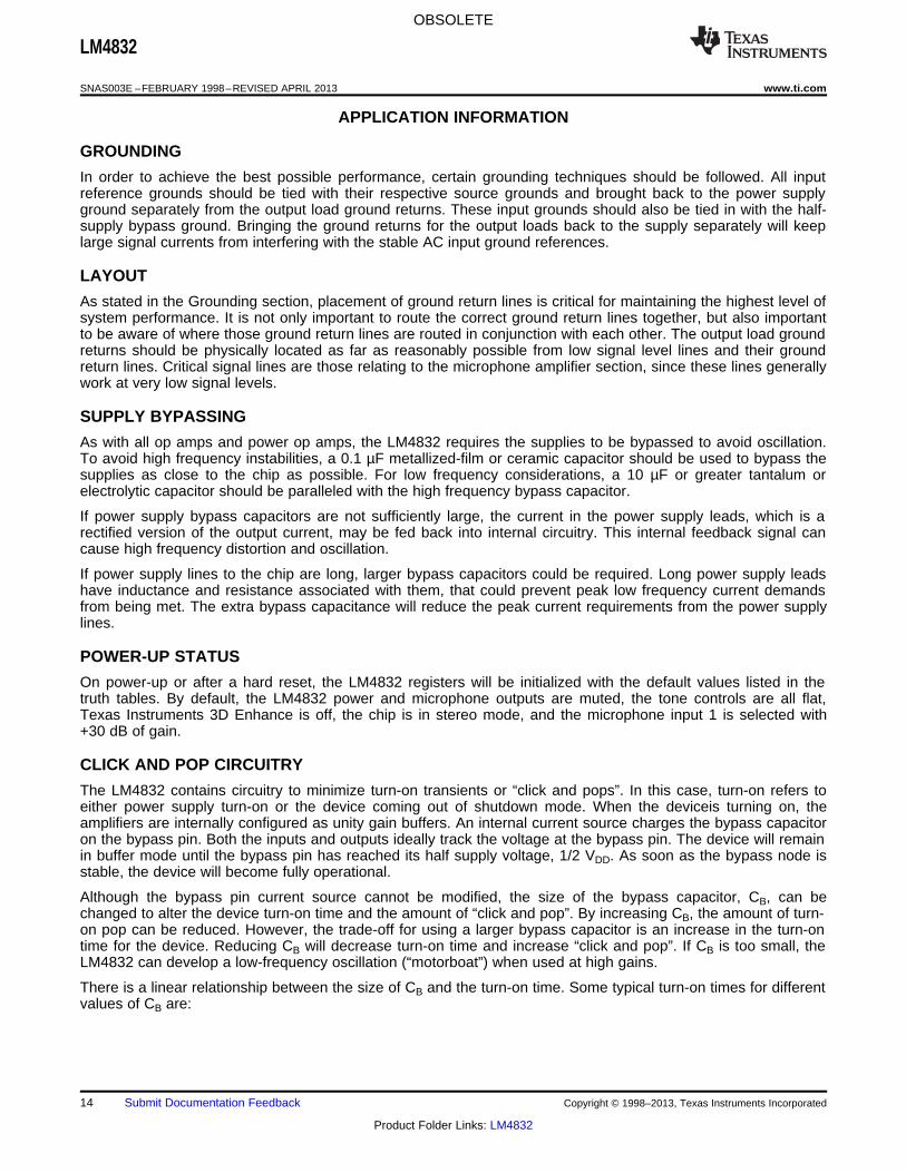
Cb TON
0.01 µF 20 ms
0.1 µF 200 ms
0.22 µF 420 ms
In order to eliminate “click and pop”, all capacitors must be discharged before turn-on. Rapid on/off switching ofthe device or shutdown function may cause the “click and pop” circuitry to not operate fully, resulting in increased“click and pop” noise. The output coupling cap, CO, is of particular concern. This capacitor discharges through aninternal 20 kΩ resistor. Depending on the size of CO, the time constant can be quite large. To reduce transients,an external 1 kΩ–5 kΩ resistor can be placed in parallel with the internal 20 kΩ resistor. The tradeoff for usingthis resistor is an increase in quiescent current.
COUPLING CAPACITORS
Because the LM4832 is a single supply circuit, all audio signals must be capacitor coupled to the chip to removethe 2.5 VDC bias. All audio inputs have 20 kΩ input impedances, so the AC-coupling capacitor will create a high-pass filter with
f−3dB = 1/(2π*20 kΩ*CIN). (1)
The amplifier outputs also need to be AC-coupled to the loads.The high-pass filter is comprised of the outputload and the coupling capacitor,where the filter cutoff is at
f−3dB = 1/(2π*RLOAD*COUT). (2)
POWER AMPLIFIER
The power amplifiers in the LM4832 are designed to drive 8Ω or 32Ω loads at 200 mW (continuous) and 75 mW(continuous), respectively, with 1% THD+N. As shown in the Typical Performance Characteristics, the poweramplifiers typically drive 4Ω loads at 350 mW, but with a slight increase in high-frequency THD. As discussedabove, these outputs should be AC-coupled to the output load.
MICROPHONE AMPLIFIER
The microphone preamplifier is intended to amplify low-level signals for signal conditioning. The microphoneinputs can be directly connected to microphone networks. The microphone amplifier has enough output capabilityto drive a 1 kΩ load. All microphone inputs and outputs must be AC-coupled.
I2C INTERFACE
The LM4832 uses a serial bus, which conforms to the I2C protocol, to control the chip's functions with two wires:clock and data. The clock line is uni-directional. The data line is bi-directional(open-collector) with a pullupresistor (typically 10 kΩ).The maximum clock frequency specified by the I2C standard is 400 kHz. In thisdiscussion, the master is the controlling microcontroller and the slave is the LM4832.
The I2C address for the LM4832 is determined using the Address Bit 1 and Address Bit 2 TTL/CMOS inputs onthe chip. The LM4832's four possible I2C chip addresses are of the form 10000X2X10 (binary), where the X2 andX1bits are determined by the voltage levels at the Address Bit 2 and Address Bit 1 pins, respectively. If the I2Cinterface is used to address a number of chips in a system and the LM4832's chip address can be changed toavoid address conflicts.
The timing diagram for the I2C is shown in Figure 2. The data is latched in on the stable high level of the clockand the data line should be held high when not in use. The timing diagram is broken up into six major sections:
The “start” signal is generated by lowering the data signal while the clock signal is high. The start signal will alertall devices attached to the I2C bus to check the incoming address against their own chip address.
The 8-bit chip address is sent next, most significant bit first. Each address bit must be stable while the clock levelis high.
After the last bit of the address is sent, the master checks for the LM4832's acknowledge. The master releasesthe data line high (through a pullup resistor). Then the master sends a clock pulse. If the LM4832 has receivedthe address correctly, then it holds the data line low during the clock pulse. If the data line is not low, then themaster should send a “stop” signal (discussed later) and abort the transfer.
Copyright © 1998–2013, Texas Instruments Incorporated Submit Documentation Feedback 15
Product Folder Links: LM4832
OBSOLETE
LM4832
SNAS003E –FEBRUARY 1998–REVISED APRIL 2013 www.ti.com
The 8 bits of data are sent next, most significant bit first. Each data bit should be valid while the clock level isstable high.
After the data byte is sent, the master must generate another acknowledge to see if the LM4832 received thedata.
If the master has more data bytes to send to the LM4832, then the master can repeat the previous two stepsuntil all data bytes have been sent.
The “stop” signal ends the transfer. To signal “stop”, the data signal goes high while the clock signal is high.
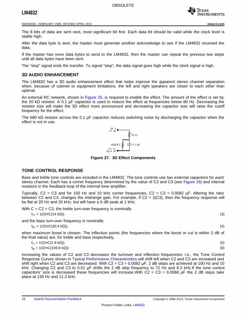
3D AUDIO ENHANCEMENT
The LM4832 has a 3D audio enhancement effect that helps improve the apparent stereo channel separationwhen, because of cabinet or equipment limitations, the left and right speakers are closer to each other thanoptimal.
An external RC network, shown in Figure 25, is required to enable the effect. The amount of the effect is set bythe 20 kΩ resistor. A 0.1 µF capacitor is used to reduce the effect at frequencies below 80 Hz. Decreasing theresistor size will make the 3D effect more pronounced and decreasing the capacitor size will raise the cutofffrequency for the effect.
The 680 kΩ resistor across the 0.1 µF capacitor reduces switching noise by discharging the capacitor when theeffect is not in use.
Figure 27. 3D Effect Components
TONE CONTROL RESPONSE
Bass and treble tone controls are included in the LM4832. The tone controls use two external capacitors for eachstereo channel. Each has a corner frequency determined by the value of C2 and C3 (see Figure 26) and internalresistors in the feedback loop of the internal tone amplifier.
Typically, C2 = C3 and for 100 Hz and 10 kHz corner frequencies, C2 = C3 = 0.0082 µF. Altering the ratiobetween C2 and C3, changes the midrange gain. For example, if C2 = 2(C3), then the frequency response willbe flat at 20 Hz and 20 kHz, but will have a 6 dB peak at 1 kHz.
With C = C2 = C3, the treble turn-over frequency is nominallyfTT = 1/(2πC(14 kΩ)) (3)
and the bass turn-over frequency is nominallyfBT = 1/(2πC(30.4 kΩ)), (4)
when maximum boost is chosen. The inflection points (the frequencies where the boost or cut is within 3 dB ofthe final value) are, for treble and bass respectively,
fTI = 1/(2πC(1.9 kΩ)) (5)fBI = 1/(2πC(169.6 kΩ)) (6)
Increasing the values of C2 and C3 decreases the turnover and inflection frequencies: i.e., the Tone ControlResponse Curves shown in Typical Performance Characteristics will shift left when C2 and C3 are increased andshift right when C2 and C3 are decreased. With C2 = C3 = 0.0082 μF, 2 dB steps are achieved at 100 Hz and 10kHz. Changing C2 and C3 to 0.01 μF shifts the 2 dB step frequency to 72 Hz and 8.3 kHz.If the tone controlcapacitors' size is decreased these frequencies will increase.With C2 = C3 = 0.0068 μF the 2 dB steps takeplace at 130 Hz and 11.2 kHz.
16 Submit Documentation Feedback Copyright © 1998–2013, Texas Instruments Incorporated
Product Folder Links: LM4832
OBSOLETE
LM4832
www.ti.com SNAS003E –FEBRUARY 1998–REVISED APRIL 2013
Figure 28. Tone Control Diagram
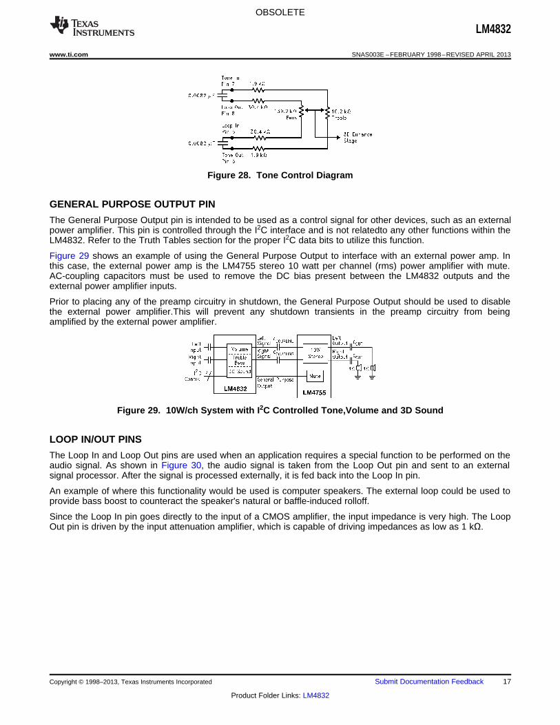
GENERAL PURPOSE OUTPUT PIN
The General Purpose Output pin is intended to be used as a control signal for other devices, such as an externalpower amplifier. This pin is controlled through the I2C interface and is not relatedto any other functions within theLM4832. Refer to the Truth Tables section for the proper I2C data bits to utilize this function.
Figure 29 shows an example of using the General Purpose Output to interface with an external power amp. Inthis case, the external power amp is the LM4755 stereo 10 watt per channel (rms) power amplifier with mute.AC-coupling capacitors must be used to remove the DC bias present between the LM4832 outputs and theexternal power amplifier inputs.
Prior to placing any of the preamp circuitry in shutdown, the General Purpose Output should be used to disablethe external power amplifier.This will prevent any shutdown transients in the preamp circuitry from beingamplified by the external power amplifier.
Figure 29. 10W/ch System with I2C Controlled Tone,Volume and 3D Sound
LOOP IN/OUT PINS
The Loop In and Loop Out pins are used when an application requires a special function to be performed on theaudio signal. As shown in Figure 30, the audio signal is taken from the Loop Out pin and sent to an externalsignal processor. After the signal is processed externally, it is fed back into the Loop In pin.
An example of where this functionality would be used is computer speakers. The external loop could be used toprovide bass boost to counteract the speaker's natural or baffle-induced rolloff.
Since the Loop In pin goes directly to the input of a CMOS amplifier, the input impedance is very high. The LoopOut pin is driven by the input attenuation amplifier, which is capable of driving impedances as low as 1 kΩ.
Copyright © 1998–2013, Texas Instruments Incorporated Submit Documentation Feedback 17
Product Folder Links: LM4832
OBSOLETE
LM4832
SNAS003E –FEBRUARY 1998–REVISED APRIL 2013 www.ti.com
Figure 30.
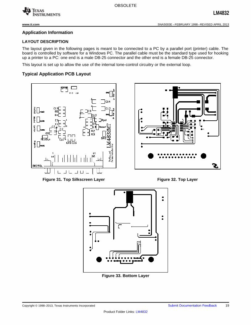
LM4832 SAMPLE LAYOUT
LAYOUT PARTS LIST
Name Type Quantity
Capacitors:
C1 1µF, Tantalum, 16V, 10% 1
C2 0.1µF, Tantalum, 16V, 10% 1
C3 0.1µF, Tantalum, 16V, 10% 1
C4 1µF, Tantalum, 16V, 10% 1
C5 8200pF, Ceramic, 50V, 10% 1
C6 8200pF, Ceramic, 50V, 10% 1
C7 1µF, Tantalum, 16V, 10% 1
C8 1µF, Tantalum, 16V, 10% 1
C9 1µF, Tantalum, 16V, 10% 1
C10 10µF, Tantalum, 16V, 10% 1
C11 1µF, Tantalum, 16V, 10% 1
C12 470µF, Size D; or 300µF, 10V 1
C13 0.1µF, Tantalum, 50V, 10% 1
C14 470µF, Size D; 300µF, 10V 1
C15 8200pF, Ceramic, 50V, 10% 1
C16 8200pF, Ceramic, 50V, 10% 1
Resistors:
RPD 1kΩ, 1/8W 1
RDGND 100Ω, 1/8W 1
R2 10kΩ, 1/8W 1
R3 10kΩ, 1/8W 1
R4 20kΩ, 1/8W 1
R5 680kΩ, 1/8W 1
Connectors:
HDR 2X1 100mil 9
DB25SL connector - male 1
18 Submit Documentation Feedback Copyright © 1998–2013, Texas Instruments Incorporated
Product Folder Links: LM4832
OBSOLETE
LM4832
www.ti.com SNAS003E –FEBRUARY 1998–REVISED APRIL 2013
Application Information
LAYOUT DESCRIPTION
The layout given in the following pages is meant to be connected to a PC by a parallel port (printer) cable. Theboard is controlled by software for a Windows PC. The parallel cable must be the standard type used for hookingup a printer to a PC: one end is a male DB-25 connector and the other end is a female DB-25 connector.
This layout is set up to allow the use of the internal tone-control circuitry or the external loop.
Typical Application PCB Layout
Figure 31. Top Silkscreen Layer Figure 32. Top Layer
Figure 33. Bottom Layer
Copyright © 1998–2013, Texas Instruments Incorporated Submit Documentation Feedback 19
Product Folder Links: LM4832
OBSOLETE
LM4832
SNAS003E –FEBRUARY 1998–REVISED APRIL 2013 www.ti.com
REVISION HISTORY
Changes from Revision D (April 2013) to Revision E Page
• Changed layout of National Data Sheet to TI format .......................................................................................................... 19
20 Submit Documentation Feedback Copyright © 1998–2013, Texas Instruments Incorporated
Product Folder Links: LM4832
IMPORTANT NOTICE
Texas Instruments Incorporated and its subsidiaries (TI) reserve the right to make corrections, enhancements, improvements and otherchanges to its semiconductor products and services per JESD46, latest issue, and to discontinue any product or service per JESD48, latestissue. Buyers should obtain the latest relevant information before placing orders and should verify that such information is current andcomplete. All semiconductor products (also referred to herein as “components”) are sold subject to TI’s terms and conditions of salesupplied at the time of order acknowledgment.
TI warrants performance of its components to the specifications applicable at the time of sale, in accordance with the warranty in TI’s termsand conditions of sale of semiconductor products. Testing and other quality control techniques are used to the extent TI deems necessaryto support this warranty. Except where mandated by applicable law, testing of all parameters of each component is not necessarilyperformed.
TI assumes no liability for applications assistance or the design of Buyers’ products. Buyers are responsible for their products andapplications using TI components. To minimize the risks associated with Buyers’ products and applications, Buyers should provideadequate design and operating safeguards.
TI does not warrant or represent that any license, either express or implied, is granted under any patent right, copyright, mask work right, orother intellectual property right relating to any combination, machine, or process in which TI components or services are used. Informationpublished by TI regarding third-party products or services does not constitute a license to use such products or services or a warranty orendorsement thereof. Use of such information may require a license from a third party under the patents or other intellectual property of thethird party, or a license from TI under the patents or other intellectual property of TI.
Reproduction of significant portions of TI information in TI data books or data sheets is permissible only if reproduction is without alterationand is accompanied by all associated warranties, conditions, limitations, and notices. TI is not responsible or liable for such altereddocumentation. Information of third parties may be subject to additional restrictions.
Resale of TI components or services with statements different from or beyond the parameters stated by TI for that component or servicevoids all express and any implied warranties for the associated TI component or service and is an unfair and deceptive business practice.TI is not responsible or liable for any such statements.
Buyer acknowledges and agrees that it is solely responsible for compliance with all legal, regulatory and safety-related requirementsconcerning its products, and any use of TI components in its applications, notwithstanding any applications-related information or supportthat may be provided by TI. Buyer represents and agrees that it has all the necessary expertise to create and implement safeguards whichanticipate dangerous consequences of failures, monitor failures and their consequences, lessen the likelihood of failures that might causeharm and take appropriate remedial actions. Buyer will fully indemnify TI and its representatives against any damages arising out of the useof any TI components in safety-critical applications.
In some cases, TI components may be promoted specifically to facilitate safety-related applications. With such components, TI’s goal is tohelp enable customers to design and create their own end-product solutions that meet applicable functional safety standards andrequirements. Nonetheless, such components are subject to these terms.
No TI components are authorized for use in FDA Class III (or similar life-critical medical equipment) unless authorized officers of the partieshave executed a special agreement specifically governing such use.
Only those TI components which TI has specifically designated as military grade or “enhanced plastic” are designed and intended for use inmilitary/aerospace applications or environments. Buyer acknowledges and agrees that any military or aerospace use of TI componentswhich have not been so designated is solely at the Buyer's risk, and that Buyer is solely responsible for compliance with all legal andregulatory requirements in connection with such use.
TI has specifically designated certain components as meeting ISO/TS16949 requirements, mainly for automotive use. In any case of use ofnon-designated products, TI will not be responsible for any failure to meet ISO/TS16949.
Products Applications
Audio www.ti.com/audio Automotive and Transportation www.ti.com/automotive
Amplifiers amplifier.ti.com Communications and Telecom www.ti.com/communications
Data Converters dataconverter.ti.com Computers and Peripherals www.ti.com/computers
DLP® Products www.dlp.com Consumer Electronics www.ti.com/consumer-apps
DSP dsp.ti.com Energy and Lighting www.ti.com/energy
Clocks and Timers www.ti.com/clocks Industrial www.ti.com/industrial
Interface interface.ti.com Medical www.ti.com/medical
Logic logic.ti.com Security www.ti.com/security
Power Mgmt power.ti.com Space, Avionics and Defense www.ti.com/space-avionics-defense
Microcontrollers microcontroller.ti.com Video and Imaging www.ti.com/video
RFID www.ti-rfid.com
OMAP Applications Processors www.ti.com/omap TI E2E Community e2e.ti.com
Wireless Connectivity www.ti.com/wirelessconnectivity
Mailing Address: Texas Instruments, Post Office Box 655303, Dallas, Texas 75265Copyright © 2013, Texas Instruments Incorporated