Embed Size (px)
Citation preview

May 14, 2008
LM4752Stereo 11W Audio Power AmplifierGeneral DescriptionThe LM4752 is a stereo audio amplifier capable of delivering11W per channel of continuous average output power to a4Ω load, or 7W per channel into 8Ω using a single 24V supplyat 10% THD+N.
The LM4752 is specifically designed for single supply opera-tion and a low external component count. The gain and biasresistors are integrated on chip, resulting in a 11W stereoamplifier in a compact 7 pin TO220 package. High outputpower levels at both 20V and 24V supplies and low externalcomponent count offer high value for compact stereo and TVapplications. A simple mute function can be implemented withthe addition of a few external components.
Key Specifications Output power at 10% THD+N with 1kHz into 4Ω at
VCC = 24V: 11W (typ)
Output power at 10% THD+N with 1kHz into 8Ω atVCC = 24V: 7W (typ)
Closed loop gain: 34dB (typ)
PO at 10% THD+N @ 1 kHz into 4Ω single-ended TO-263package at VCC = 12V: 2.5W (typ)
PO at 10% THD+N @ 1kHz into 8Ω bridged TO-263package at VCC = 12V: 5W (typ)
Features Drives 4Ω and 8Ω loads
Internal gain resistors (AV = 34 dB)
Minimum external component requirement
Single supply operation
Internal current limiting
Internal thermal protection
Compact 7-lead TO-220 package
Low cost-per-watt
Wide supply range 9V - 40V
Applications Compact stereos
Stereo TVs
Mini component stereos
Multimedia speakers
Typical Application
10003901
FIGURE 1. Typical Audio Amplifier Application Circuit
© 2008 National Semiconductor Corporation 100039 www.national.com
LM
4752 S
tere
o 1
1W
Au
dio
Po
wer A
mp
lifier

Connection Diagrams
Plastic Package
10003902
Package DescriptionTop View
Order Number LM4752TPackage Number TA07B
10003950
Package DescriptionTop View
Order Number LM4752TSPackage Number TS07B
www.national.com 2
LM
4752

Absolute Maximum Ratings (Note 2)
If Military/Aerospace specified devices are required,please contact the National Semiconductor Sales Office/Distributors for availability and specifications.
Supply Voltage 40V
Input Voltage ±0.7V
Input Voltage at Output Pins (Note 8) GND – 0.4V
Output Current Internally Limited
Power Dissipation (Note 3) 62.5W
ESD Susceptibility (Note 4) 2 kV
Junction Temperature 150°C
Soldering Information T Package (10 sec) 250°C
Storage Temperature −40°C to 150°C
Operating RatingsTemperature Range
TMIN ≤ TA ≤ TMAX −40°C ≤ TA ≤ +85°C
Supply Voltage 9V to 32V
θJC 2°C/W
θJA 79°C/W
Electrical CharacteristicsThe following specifications apply to each channel with VCC = 24V, TA = 25°C unless otherwise specified.
Symbol Parameter Conditions
LM4752Units
(Limits)Typical
(Note 5)
Limit
(Note 6)
Itotal Total Quiescent Power Supply
CurrentVINAC = 0V, Vo = 0V, RL = ∞ 10.5 20 mA(max)
7 mA(min)
Po Output Power (Continuous f = 1 kHz, THD+N = 10%, RL = 8Ω 7 W
Average per Channel) f = 1 kHz, THD+N = 10%, RL = 4Ω 10 W(min)
VCC = 20V, RL = 8Ω 4 W
VCC = 20V, R L = 4Ω 7 W
f = 1 kHz, THD+N = 10%, RL = 4ΩVS = 12V, TO-263 Pkg.
2.5 W
THD+N Total Harmonic Distortion plus Noise f = 1 kHz, Po = 1 W/ch, RL = 8Ω 0.08 %
VOSW Output Swing RL = 8Ω, V CC = 20V 15 V
RL = 4Ω, V CC = 20V 14 V
Xtalk Channel Separation See Figure 1 55 dB
f = 1 kHz, Vo = 4 Vrms, RL = 8Ω
PSRR Power Supply Rejection Ratio See Figure 1 50 dB
VCC = 22V to 26V, R L = 8Ω
VODV Differential DC Output Offset Voltage VINAC = 0V 0.09 0.4 V(max)
SR Slew Rate 2 V/µs
RIN Input Impedance 83 kΩPBW Power Bandwidth 3 dB BW at Po = 2.5W, RL = 8Ω 65 kHz
A VCL Closed Loop Gain (Internally Set) RL = 8Ω 34 33 dB(min)
35 dB(max)
ein Noise IHF-A Weighting Filter, RL = 8Ω 0.2 mVrms
Output Referred
Io Output Short Circuit Current Limit VIN = 0.5V, R L = 2Ω 2 A(min)
Note 1: All voltages are measured with respect to the GND pin (4), unless otherwise specified.
Note 2: Absolute Maximum Ratings indicate limits beyond which damage to the device may occur. Operating Ratings indicate conditions for which the deviceis functional, but do not guarantee specific performance limits. Electrical Characteristics state DC and AC electrical specifications under particular test conditionswhich guarantee specific performance limits. This assumes that the device is within the Operating Ratings. Specifications are not guaranteed for parameterswhere no limit is given, however, the typical value is a good indication of device performance.
Note 3: For operating at case temperatures above 25°C, the device must be derated based on a 150°C maximum junction temperature and a thermal resistanceof θJC = 2°C/W (junction to case). Refer to the section Determining the Maximum Power Dissipation in the Application Information section for more information.
Note 4: Human body model, 100 pF discharged through a 1.5 kΩ resistor.
Note 5: Typicals are measured at 25°C and represent the parametric norm.
Note 6: Limits are guarantees that all parts are tested in production to meet the stated values.
Note 7: The TO-263 Package is not recommended for VS > 16V due to impractical heatsinking limitations.
Note 8: The outputs of the LM4752 cannot be driven externally in any mode with a voltage lower than -0.4V below GND or permanent damage to the LM4752will result.
3 www.national.com
LM
4752

Test Circuit
10003936
FIGURE 2. Test Circuit
www.national.com 4
LM
4752

Typical Application with Mute
10003903
FIGURE 3. Application with Mute Function
5 www.national.com
LM
4752

Equivalent Schematic Diagram
10003904
www.national.com 6
LM
4752

System Application Circuit
10003905
FIGURE 4. Circuit for External Components Description
External Components Description
Components Function Description
1, 2 Cs Provides power supply filtering and bypassing.
3, 4 Rsn Works with Csn to stabilize the output stage from high frequency oscillations.
5, 6 Csn Works with Rsn to stabilize the output stage from high frequency oscillations.
7 Cb Provides filtering for the internally generated half-supply bias generator.
8, 9 Ci Input AC coupling capacitor which blocks DC voltage at the amplifier's input terminals. Also creates a high pass
filter with fc =1/(2 • π • Rin • Cin).
10, 11 Co Output AC coupling capacitor which blocks DC voltage at the amplifier's output terminal. Creates a high pass
filter with fc =1/(2 • π • Rout • Cout).
12, 13 Ri Voltage control - limits the voltage level to the amplifier's input terminals.
7 www.national.com
LM
4752

Typical Performance Characteristics
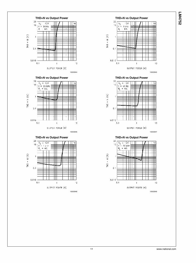
THD+N vs Output Power
10003912
THD+N vs Output Power
10003913
THD+N vs Output Power
10003914
THD+N vs Output Power
10003906
THD+N vs Output Power
10003907
THD+N vs Output Power
10003908
www.national.com 8
LM
4752

THD+N vs Output Power
10003915
THD+N vs Output Power
10003916
THD+N vs Output Power
10003917
THD+N vs Output Power
10003909
THD+N vs Output Power
10003910
THD+N vs Output Power
10003911
9 www.national.com
LM
4752

THD+N vs Output Power
10003938
THD+N vs Output Power
10003939
THD+N vs Output Power
10003940
THD+N vs Output Power
10003941
THD+N vs Output Power
10003942
THD+N vs Output Power
10003943
www.national.com 10
LM
4752
THD+N vs Output Power
10003944
THD+N vs Output Power
10003945
THD+N vs Output Power
10003946
THD+N vs Output Power
10003947
THD+N vs Output Power
10003948
THD+N vs Output Power
10003949
11 www.national.com
LM
4752
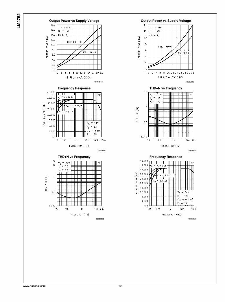
Output Power vs Supply Voltage
10003918
Output Power vs Supply Voltage
10003919
Frequency Response
10003920
THD+N vs Frequency
10003921
THD+N vs Frequency
10003922
Frequency Response
10003923
www.national.com 12
LM
4752

Channel Separation
10003924
PSRR vs Frequency
10003925
Supply Current vsSupply Voltage
10003926
Power Derating Curve
10003927
Power Dissipation vs Output Power
10003928
Power Dissipation vs Output Power
10003929
13 www.national.com
LM
4752

Power Dissipation vs Output Power
10003951
Power Dissipation vs Output Power
10003952
Application Information
CAPACITOR SELECTION AND FREQUENCY RESPONSE
With the LM4752, as in all single supply amplifiers, AC cou-pling capacitors are used to isolate the DC voltage present atthe inputs (pins 2,6) and outputs (pins 1,7). As mentionedearlier in the External Components section these capacitorscreate high-pass filters with their corresponding input/outputimpedances. The Typical Application Circuit shown in Fig-ure 1 shows input and output capacitors of 0.1 μF and 1,000μF respectively. At the input, with an 83 kΩ typical input re-sistance, the result is a high pass 3 dB point occurring at 19Hz. There is another high pass filter at 39.8 Hz created withthe output load resistance of 4Ω. Careful selection of thesecomponents is necessary to ensure that the desired frequen-cy response is obtained. The Frequency Response curves inthe Typical Performance Characteristics section show howdifferent output coupling capacitors affect the low frequencyrolloff.
APPLICATION CIRCUIT WITH MUTE
With the addition of a few external components, a simple mutecircuit can be implemented, such as the one shown in Figure3. This circuit works by externally pulling down the half supplybias line (pin 5), effectively shutting down the input stage.
When using an external circuit to pull down the bias, care mustbe taken to ensure that this line is not pulled down too quickly,or output “pops” or signal feedthrough may result. If the biasline is pulled down too quickly, currents induced in the internalbias resistors will cause a momentary DC voltage to appearacross the inputs of each amplifier's internal differential pair,
resulting in an output DC shift towards V SUPPLY. An R-C timingcircuit should be used to limit the pull-down time such thatoutput “pops” and signal feedthroughs will be minimized. Thepull-down timing is a function of a number of factors, includingthe external mute circuitry, the voltage used to activate themute, the bias capacitor, the half-supply voltage, and internalresistances used in the half-supply generator. Table 1 showsa list of recommended values for the external mute circuitry.
TABLE 1. Values for Mute Circuit
VMUTE R1 R2 C1 R3 CB VCC
5V 10 kΩ 10 kΩ 4.7 μF 360Ω 100 μF 21V–32V
VS 20 kΩ 1.2 kΩ 4.7 μF 180Ω 100 μF 15V–32V
VS 20 kΩ 910Ω 4.7 μF 180Ω 47 μF 22V–32V
OPERATING IN BRIDGE-MODE
Though designed for use as a single-ended amplifier, theLM4752 can be used to drive a load differentially (bridge-mode). Due to the low pin count of the package, only the non-inverting inputs are available. An inverted signal must beprovided to one of the inputs. This can easily be done with theuse of an inexpensive op-amp configured as a standard in-verting amplifier. An LF353 is a good low-cost choice. Caremust be taken, however, for a bridge-mode amplifier musttheoretically dissipate four times the power of a single-endedtype. The load seen by each amplifier is effectively half thatof the actual load being used, thus an amplifier designed todrive a 4Ω load in single-ended mode should drive an 8Ω loadwhen operating in bridge-mode.
www.national.com 14
LM
4752

10003930
FIGURE 5. Bridge-Mode Application
10003931 10003937
FIGURE 6. THD+N vs. POUT for Bridge-Mode Application
PREVENTING OSCILLATIONS
With the integration of the feedback and bias resistors on-chip, the LM4752 fits into a very compact package. However,due to the close proximity of the non-inverting input pins tothe corresponding output pins, the inputs should be AC ter-minated at all times. If the inputs are left floating, the amplifierwill have a positive feedback path through high impedancecoupling, resulting in a high frequency oscillation. In most ap-plications, this termination is typically provided by the previ-ous stage's source impedance. If the application will requirean external signal, the inputs should be terminated to groundwith a resistance of 50 kΩ or less on the AC side of the inputcoupling capacitors.
UNDERVOLTAGE SHUTDOWN
If the power supply voltage drops below the minimum oper-ating supply voltage, the internal under-voltage detection cir-cuitry pulls down the half-supply bias line, shutting down thepreamp section of the LM4752. Due to the wide operatingsupply range of the LM4752, the threshold is set to just under9V. There may be certain applications where a higher thresh-old voltage is desired. One example is a design requiring ahigh operating supply voltage, with large supply and bias ca-pacitors, and there is little or no other circuitry connected tothe main power supply rail. In this circuit, when the power isdisconnected, the supply and bias capacitors will dischargeat a slower rate, possibly resulting in audible output distortionas the decaying voltage begins to clip the output signal. An
15 www.national.com
LM
4752
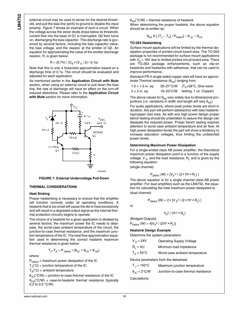
external circuit may be used to sense for the desired thresh-old, and pull the bias line (pin5) to ground to disable the inputpreamp. Figure 7 shows an example of such a circuit. Whenthe voltage across the zener diode drops below its threshold,current flow into the base of Q1 is interrupted. Q2 then turnson, discharging the bias capacitor. This discharge rate is gov-erned by several factors, including the bias capacitor value,the bias voltage, and the resistor at the emitter of Q2. Anequation for approximating the value of the emitter dischargeresistor, R, is given below:
R = (0.7V) / (CB • (V S / 2) / 0.1s)
Note that this is only a linearized approximation based on adischarge time of 0.1s. The circuit should be evaluated andadjusted for each application.
As mentioned earlier in the Application Circuit with Mutesection, when using an external circuit to pull down the biasline, the rate of discharge will have an effect on the turn-offinduced distortions. Please refer to the Application Circuitwith Mute section for more information.
10003932
FIGURE 7. External Undervoltage Pull-Down
THERMAL CONSIDERATIONS
Heat Sinking
Proper heatsinking is necessary to ensure that the amplifierwill function correctly under all operating conditions. Aheatsink that is too small will cause the die to heat excessivelyand will result in a degraded output signal as the internal ther-mal protection circuitry begins to operate.
The choice of a heatsink for a given application is dictated byseveral factors: the maximum power the IC needs to dissi-pate, the worst-case ambient temperature of the circuit, thejunction-to-case thermal resistance, and the maximum junc-tion temperature of the IC. The heat flow approximation equa-tion used in determining the correct heatsink maximumthermal resistance is given below:
TJ–TA = P DMAX • (θJC + θCS + θ SA)
where:
PDMAX = maximum power dissipation of the IC
TJ(°C) = junction temperature of the IC
TA(°C) = ambient temperature
θJC(°C/W) = junction-to-case thermal resistance of the IC
θCS(°C/W) = case-to-heatsink thermal resistance (typically0.2 to 0.5 °C/W)
θSA(°C/W) = thermal resistance of heatsink
When determining the proper heatsink, the above equationshould be re-written as:
θSA ≤ [ (TJ − TA) / PDMAX] − θ JC − θCS
TO-263 Heatsinking
Surface mount applications will be limited by the thermal dis-sipation properties of printed circuit board area. The TO-263package is not recommended for surface mount applicationswith VS > 16V due to limited printed circuit board area. Thereare TO-263 package enhancements, such as clip-onheatsinks and heatsinks with adhesives, that can be used toimprove performance.
Standard FR-4 single-sided copper clad will have an approx-imate Thermal resistance (θSA) ranging from:
1.5 × 1.5 in. sq. 20–27°C/W (TA=28°C, Sine wave
testing, 1 oz. Copper)2 × 2 in. sq. 16–23°C/W
The above values for θSA vary widely due to dimensional pro-portions (i.e. variations in width and length will vary θSA).
For audio applications, where peak power levels are short induration, this part will perform satisfactory with less heatsink-ing/copper clad area. As with any high power design properbench testing should be undertaken to assure the design candissipate the required power. Proper bench testing requiresattention to worst case ambient temperature and air flow. Athigh power dissipation levels the part will show a tendency toincrease saturation voltages, thus limiting the undistortedpower levels.
Determining Maximum Power Dissipation
For a single-ended class AB power amplifier, the theoreticalmaximum power dissipation point is a function of the supplyvoltage, V S, and the load resistance, RL and is given by thefollowing equation:
(single channel)
PDMAX (W) = [VS 2 / (2 • π2 • RL) ]
The above equation is for a single channel class-AB poweramplifier. For dual amplifiers such as the LM4752, the equa-tion for calculating the total maximum power dissipated is:
(dual channel)
PDMAX (W) = 2 • [V S2 / (2 • π2 • RL) ]
or
VS2 / (π 2 • RL)
(Bridged Outputs)
PDMAX (W) = 4[VS2 / (2π2 • RL)]
Heatsink Design Example
Determine the system parameters:
V S = 24V Operating Supply Voltage
RL = 4Ω Minimum load impedance
TA = 55°C Worst case ambient temperature
Device parameters from the datasheet:
T J = 150°C Maximum junction temperature
θJC = 2°C/W Junction-to-case thermal resistance
Calculations:
www.national.com 16
LM
4752

2 • PDMAX = 2 • [V S2 / (2 • π2 • RL) ] = (24V)2 / (2 • π2 • 4Ω) =
14.6W
θSA ≤ [ (TJ − TA) / PDMAX] − θ JC − θCS = [ (150°C − 55°C) /
14.6W ] − 2°C/W − 0.2°C/W = 4.3°C/W
Conclusion: Choose a heatsink with θSA ≤ 4.3°C/W.
TO-263 Heatsink Design Examples
Example 1: (Stereo Single-Ended Output)
Given: TA=30°C
TJ=150°C
RL=4ΩVS=12V
θJC=2°C/W
PDMAX from PD vs PO Graph:
PDMAX ≈ 3.7W
Calculating PDMAX:
PDMAX = VCC2 / (π2RL) = (12V)2 / π2(4Ω)) = 3.65W
Calculating Heatsink Thermal Resistance:
θSA < [(T J − TA) / PDMAX] − θJC − θCS
θSA < 120°C / 3.7W − 2.0°C/W − 0.2°C/W = 30.2°C/W
Therefore the recommendation is to use 1.5 × 1.5 square inchof single-sided copper clad.
Example 2: (Stereo Single-Ended Output)
Given: TA=50°C
TJ=150°C
RL=4ΩVS=12V
θJC=2°C/W
PDMAX from PD vs PO Graph:
PDMAX ≈ 3.7W
Calculating PDMAX:
PDMAX = VCC2 / (π2RL) = (12V)2 / (π2(4Ω)) = 3.65W
Calculating Heatsink Thermal Resistance:
θSA < [(TJ − TA) / PDMAX] − θJC − θCS
θSA < 100°C / 3.7W − 2.0°C/W − 0.2°C/W = 24.8°C/W
Therefore the recommendation is to use 2.0 × 2.0 square inchof single-sided copper clad.
Example 3: (Bridged Output)
Given: TA=50°C
TJ=150°C
RL=8ΩVS=12V
θJC=2°C/W
Calculating PDMAX:
PDMAX = 4[VCC2 / (2π2RL)] = 4(12V)2 / (2π2(8Ω)) = 3.65W
Calculating Heatsink Thermal Resistance:
θSA < [(TJ − TA) / PDMAX] − θJC − θCS
θSA < 100°C / 3.7W − 2.0°C/W − 0.2°C/W = 24.8°C/W
Therefore the recommendation is to use 2.0 × 2.0 square inchof single-sided copper clad.
Layout and Ground Returns
Proper PC board layout is essential for good circuit perfor-mance. When laying out a PC board for an audio poweramplifer, particular attention must be paid to the routing of theoutput signal ground returns relative to the input signal andbias capacitor grounds. To prevent any ground loops, theground returns for the output signals should be routed sepa-rately and brought together at the supply ground. The inputsignal grounds and the bias capacitor ground line should alsobe routed separately. The 0.1 μF high frequency supply by-pass capacitor should be placed as close as possible to theIC.
17 www.national.com
LM
4752

PC BOARD LAYOUT—COMPOSITE
10003933
www.national.com 18
LM
4752

PC BOARD LAYOUT—SILK SCREEN
10003934
19 www.national.com
LM
4752

PC BOARD LAYOUT—SOLDER SIDE
10003935
www.national.com 20
LM
4752
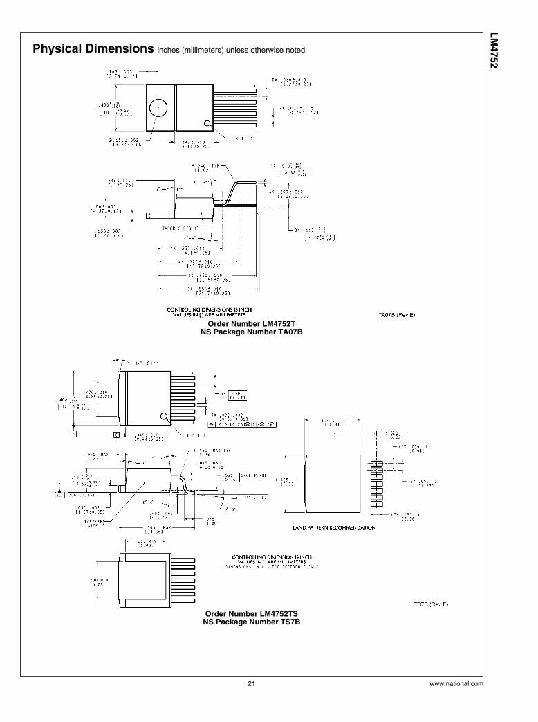
Physical Dimensions inches (millimeters) unless otherwise noted
Order Number LM4752TNS Package Number TA07B
Order Number LM4752TSNS Package Number TS7B
21 www.national.com
LM
4752

NotesL
M4752 S
tere
o 1
1W
Au
dio
Po
wer
Am
plifi
er
For more National Semiconductor product information and proven design tools, visit the following Web sites at:
Products Design Support
Amplifiers www.national.com/amplifiers WEBENCH www.national.com/webench
Audio www.national.com/audio Analog University www.national.com/AU
Clock Conditioners www.national.com/timing App Notes www.national.com/appnotes
Data Converters www.national.com/adc Distributors www.national.com/contacts
Displays www.national.com/displays Green Compliance www.national.com/quality/green
Ethernet www.national.com/ethernet Packaging www.national.com/packaging
Interface www.national.com/interface Quality and Reliability www.national.com/quality
LVDS www.national.com/lvds Reference Designs www.national.com/refdesigns
Power Management www.national.com/power Feedback www.national.com/feedback
Switching Regulators www.national.com/switchers
LDOs www.national.com/ldo
LED Lighting www.national.com/led
PowerWise www.national.com/powerwise
Serial Digital Interface (SDI) www.national.com/sdi
Temperature Sensors www.national.com/tempsensors
Wireless (PLL/VCO) www.national.com/wireless
THE CONTENTS OF THIS DOCUMENT ARE PROVIDED IN CONNECTION WITH NATIONAL SEMICONDUCTOR CORPORATION(“NATIONAL”) PRODUCTS. NATIONAL MAKES NO REPRESENTATIONS OR WARRANTIES WITH RESPECT TO THE ACCURACYOR COMPLETENESS OF THE CONTENTS OF THIS PUBLICATION AND RESERVES THE RIGHT TO MAKE CHANGES TOSPECIFICATIONS AND PRODUCT DESCRIPTIONS AT ANY TIME WITHOUT NOTICE. NO LICENSE, WHETHER EXPRESS,IMPLIED, ARISING BY ESTOPPEL OR OTHERWISE, TO ANY INTELLECTUAL PROPERTY RIGHTS IS GRANTED BY THISDOCUMENT.
TESTING AND OTHER QUALITY CONTROLS ARE USED TO THE EXTENT NATIONAL DEEMS NECESSARY TO SUPPORTNATIONAL’S PRODUCT WARRANTY. EXCEPT WHERE MANDATED BY GOVERNMENT REQUIREMENTS, TESTING OF ALLPARAMETERS OF EACH PRODUCT IS NOT NECESSARILY PERFORMED. NATIONAL ASSUMES NO LIABILITY FORAPPLICATIONS ASSISTANCE OR BUYER PRODUCT DESIGN. BUYERS ARE RESPONSIBLE FOR THEIR PRODUCTS ANDAPPLICATIONS USING NATIONAL COMPONENTS. PRIOR TO USING OR DISTRIBUTING ANY PRODUCTS THAT INCLUDENATIONAL COMPONENTS, BUYERS SHOULD PROVIDE ADEQUATE DESIGN, TESTING AND OPERATING SAFEGUARDS.
EXCEPT AS PROVIDED IN NATIONAL’S TERMS AND CONDITIONS OF SALE FOR SUCH PRODUCTS, NATIONAL ASSUMES NOLIABILITY WHATSOEVER, AND NATIONAL DISCLAIMS ANY EXPRESS OR IMPLIED WARRANTY RELATING TO THE SALEAND/OR USE OF NATIONAL PRODUCTS INCLUDING LIABILITY OR WARRANTIES RELATING TO FITNESS FOR A PARTICULARPURPOSE, MERCHANTABILITY, OR INFRINGEMENT OF ANY PATENT, COPYRIGHT OR OTHER INTELLECTUAL PROPERTYRIGHT.
LIFE SUPPORT POLICY
NATIONAL’S PRODUCTS ARE NOT AUTHORIZED FOR USE AS CRITICAL COMPONENTS IN LIFE SUPPORT DEVICES ORSYSTEMS WITHOUT THE EXPRESS PRIOR WRITTEN APPROVAL OF THE CHIEF EXECUTIVE OFFICER AND GENERALCOUNSEL OF NATIONAL SEMICONDUCTOR CORPORATION. As used herein:
Life support devices or systems are devices which (a) are intended for surgical implant into the body, or (b) support or sustain life andwhose failure to perform when properly used in accordance with instructions for use provided in the labeling can be reasonably expectedto result in a significant injury to the user. A critical component is any component in a life support device or system whose failure to performcan be reasonably expected to cause the failure of the life support device or system or to affect its safety or effectiveness.
National Semiconductor and the National Semiconductor logo are registered trademarks of National Semiconductor Corporation. All otherbrand or product names may be trademarks or registered trademarks of their respective holders.
Copyright© 2008 National Semiconductor Corporation
For the most current product information visit us at www.national.com
National SemiconductorAmericas TechnicalSupport CenterEmail: [email protected]: 1-800-272-9959
National Semiconductor EuropeTechnical Support CenterEmail: [email protected] Tel: +49 (0) 180 5010 771English Tel: +44 (0) 870 850 4288
National Semiconductor AsiaPacific Technical Support CenterEmail: [email protected]
National Semiconductor JapanTechnical Support CenterEmail: [email protected]
www.national.com