Embed Size (px)
Citation preview
LM2941QML, LM2941QML-SP
www.ti.com SNVS390B –AUGUST 2009–REVISED APRIL 2013
LM2941QML 1A Low Dropout Adjustable RegulatorCheck for Samples: LM2941QML, LM2941QML-SP
1FEATURES DESCRIPTIONThe LM2941 positive voltage regulator features the
2• Available with Radiation Ensureability to source 1A of output current with a typical
– ELDRS Free 100 krad(Si) dropout voltage of 0.5V and a maximum of 1V over• Output Voltage Adjustable from 5V to 20V the entire temperature range. Furthermore, a
quiescent current reduction circuit has been included• Dropout Voltage Typically 0.5V at IO = 1Awhich reduces the ground pin current when the• Output Current in Excess of 1A differential between the input voltage and the output
• Trimmed Reference Voltage voltage exceeds approximately 3V. The quiescentcurrent with 1A of output current and an input-output• Reverse Battery Protectiondifferential of 5V is therefore only 30mA. Higher• Internal Short Circuit Current Limitquiescent currents only exist when the regulator is in
• Mirror Image Insertion Protection the dropout mode (VI − VO ≤ 3V).• TTL, CMOS Compatible ON/OFF Switch Originally designed for vehicular applications, the
LM2941 and all regulated circuitry are protected fromreverse battery installations or two-battery jumps.During line transients, such as load dump when theinput voltage can momentarily exceed the specifiedmaximum operating voltage, the regulator willautomatically shut down to protect both the internalcircuits and the load. Familiar regulator features suchas short circuit and thermal overload protection arealso provided.
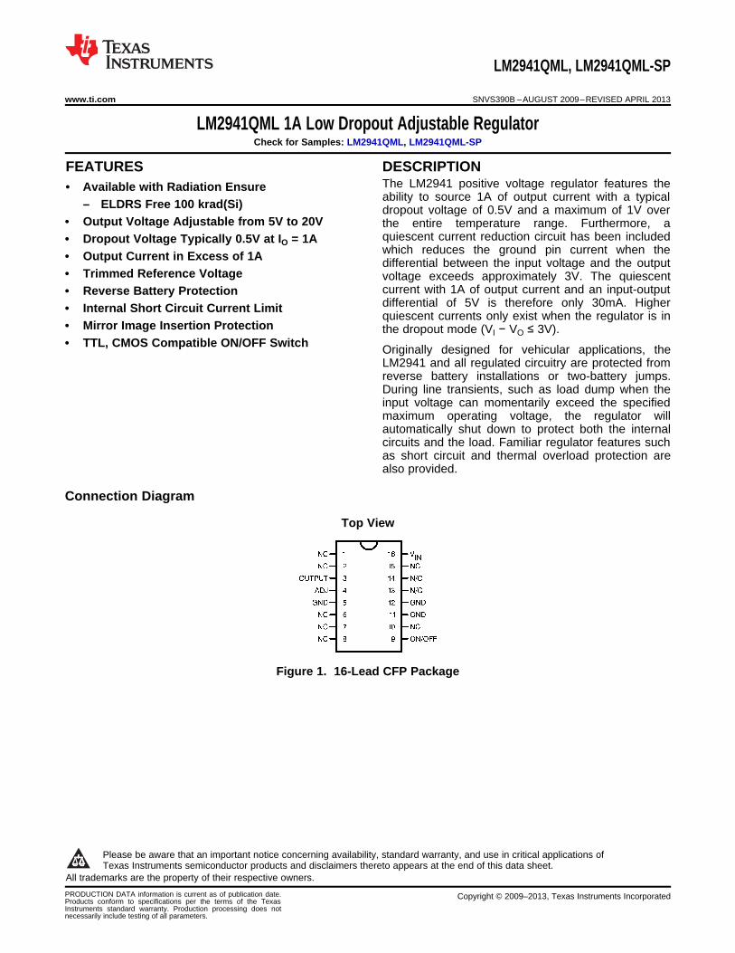
Connection Diagram
Top View
Figure 1. 16-Lead CFP Package
1
Please be aware that an important notice concerning availability, standard warranty, and use in critical applications ofTexas Instruments semiconductor products and disclaimers thereto appears at the end of this data sheet.
2All trademarks are the property of their respective owners.
PRODUCTION DATA information is current as of publication date. Copyright © 2009–2013, Texas Instruments IncorporatedProducts conform to specifications per the terms of the TexasInstruments standard warranty. Production processing does notnecessarily include testing of all parameters.
LM2941QML, LM2941QML-SP
SNVS390B –AUGUST 2009–REVISED APRIL 2013 www.ti.com
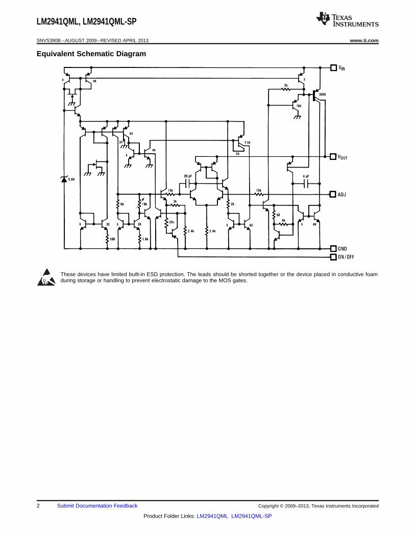
Equivalent Schematic Diagram
These devices have limited built-in ESD protection. The leads should be shorted together or the device placed in conductive foamduring storage or handling to prevent electrostatic damage to the MOS gates.
2 Submit Documentation Feedback Copyright © 2009–2013, Texas Instruments Incorporated
Product Folder Links: LM2941QML LM2941QML-SP
LM2941QML, LM2941QML-SP
www.ti.com SNVS390B –AUGUST 2009–REVISED APRIL 2013
Absolute Maximum Ratings (1)
Input Voltage (Survival Voltage, ≤ 100ms) 60V
Internal Power Dissipation (2) Internally Limited
Maximum Junction Temperature 150°C
Storage Temperature Range −65°C ≤ TJ ≤ +150°C
Lead Temperature (Soldering, 10 seconds) 300°C
CFP "WG" (device 01, 02) (Still Air) 122°C/W
CFP "WG" (device 01, 02) (500LF/Min Air Flow) 77°C/WθJA
CFP "GW" (device 03, 04) (Still Air) 136°C/WThermal Resistance
CFP "GW" (device 03, 04) (500LF/Min Air Flow) 87°C/W
CFP "WG" (device 01, 02) (3) 5°C/WθJC
CFP "GW" (device 03, 04) 13°C/W
CFP "WG" (device 01, 02) 360mgPackage Weight (Typ)
CFP "GW" (device 03, 04) 410mg
ESD susceptibility to be determined (4) 500V
(1) Absolute Maximum Ratings indicate limits beyond which damage to the device may occur. Operating Ratings indicate conditions forwhich the device is functional, but do not ensure specific performance limits. For specified specifications and test conditions, see theElectrical Characteristics. The ensured specifications apply only for the test conditions listed. Some performance characteristics maydegrade when the device is not operated under the listed test conditions.
(2) The maximum power dissipation must be derated at elevated temperatures and is dictated by TJmax (maximum junction temperature),θJA (package junction to ambient thermal resistance), and TA (ambient temperature). The maximum allowable power dissipation at anytemperature is PDmax = (TJmax - TA)/θJA or the number given in the Absolute Maximum Ratings, whichever is lower.
(3) The package material for these devices allows much improved heat transfer over our standard ceramic packages. In order to take fulladvantage of this improved heat transfer, heat sinking must be provided between the package base (directly beneath the die), and eithermetal traces on, or thermal vias through, the printed circuit board. Without this additional heat sinking, device power dissipation must becalculated using θJA, rather than θJC, thermal resistance. It must not be assumed that the device leads will provide substantial heattransfer out of the package, since the thermal resistance of the lead frame material is very poor, relative to the material of the packagebase. The stated θJC thermal resistance is for the package material only, and does not account for the additional thermal resistancebetween the package base and the printed circuit board. The user must determine the value of the additional thermal resistance andmust combine this with the stated value for the package, to calculate the total allowed power dissipation for the device.
(4) Human body model, 1.5 kΩ in series with 100 pF.
Recommended Operating ConditionsMaximum Input Voltage 26V
Temperature Range −55°C ≤ TA ≤ 125°C
Copyright © 2009–2013, Texas Instruments Incorporated Submit Documentation Feedback 3
Product Folder Links: LM2941QML LM2941QML-SP
LM2941QML, LM2941QML-SP
SNVS390B –AUGUST 2009–REVISED APRIL 2013 www.ti.com
Table 1. Quality Conformance Inspection Mil-Std-883, Method 5005 - Group A
Subgroup Description Temp °C
1 Static tests at +25
2 Static tests at +125
3 Static tests at -55
4 Dynamic tests at +25
5 Dynamic tests at +125
6 Dynamic tests at -55
7 Functional tests at +25
8A Functional tests at +125
8B Functional tests at -55
9 Switching tests at +25
10 Switching tests at +125
11 Switching tests at -55
12 Settling time at +25
13 Settling time at +125
14 Settling time at -55
LM2941 Electrical Characteristics DC ParametersThe following conditions apply, unless otherwise specified.DC: 5V ≤ VO ≤ 20V, VIN = VO+5V, CO = 22µF
Sub-Parameter Test Conditions Notes Min Max Unit groups
VRef 1.237 1.313 V 1Reference Voltage 5mA ≤ IO ≤ 1A
1.211 1.339 V 2, 3
VRLine Line Regulation VO + 2V ≤ VIN ≤ 26V, IO = 5mA See (1) 10 mV/V 1, 2, 3
50mA ≤ IO ≤ 1A, VIN = 10V, 10 mV/V 1, 2, 3VOUT = 5VVRLoad Load Regulation See (1)
50mA ≤ IO ≤ 1A, VIN = 25V, 10 mV/V 1, 2, 3VOUT = 20V
15 mA 1VO + 2V ≤ VIN ≤ 26V, IO = 5mA
20 mA 2, 3IQ Quiescent Current
45 mA 1VIN = VO + 5V, IO = 1A
60 mA 2, 3
0.8 V 1IO = 1A
1.0 V 2, 3VDO Dropout Voltage
200 mV 1IO = 100mA
300 mV 2, 3
1.6 3.5 A 1ISC Short Circuit Current VIN Max = 26V
1.3 3.7 A 2, 3
Maximum Operational Input 26 VDC 1, 2, 3See (2)Voltage
Reverse Polarity DC Input Voltage RO = 100Ω, VO ≥ -0.6V See (3) -15 V 1, 2, 3
VTH On ON/OFF Threshold Voltage ON IO ≤ 1A See (3) 0.8 V 1, 2, 3
VTh Off ON/OFF Threshold Voltage OFF IO ≤ 1A See (3) 2.00 V 1, 2, 3
100 µA 1ON/OFF Threshold Current VON/OFF = 2.0V, IO ≤ 1A
300 µA 2, 3
(1) Limit = mV per volt of VO.(2) Condition for VIN(3) Functional test go-no-go only.
4 Submit Documentation Feedback Copyright © 2009–2013, Texas Instruments Incorporated
Product Folder Links: LM2941QML LM2941QML-SP
LM2941QML, LM2941QML-SP
www.ti.com SNVS390B –AUGUST 2009–REVISED APRIL 2013
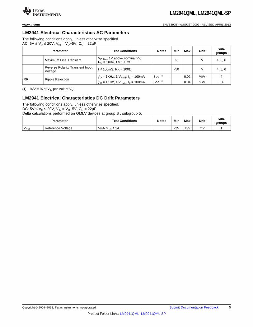
LM2941 Electrical Characteristics AC ParametersThe following conditions apply, unless otherwise specified.AC: 5V ≤ VO ≤ 20V, VIN = VO+5V, CO = 22µF
Sub-Parameter Test Conditions Notes Min Max Unit groups
VO Max 1V above nominal VO,Maximum Line Transient 60 V 4, 5, 6RO = 100Ω, t ≤ 100mS
Reverse Polarity Transient Input t ≤ 100mS, RO = 100Ω -50 V 4, 5, 6Voltage
ƒO = 1KHz, 1 VRMS, IL = 100mA See (1) 0.02 %/V 4RR Ripple Rejection
ƒO = 1KHz, 1 VRMS, IL = 100mA See (1) 0.04 %/V 5, 6
(1) %/V = % of VIN per Volt of VO.
LM2941 Electrical Characteristics DC Drift ParametersThe following conditions apply, unless otherwise specified.DC: 5V ≤ VO ≤ 20V, VIN = VO+5V, CO = 22µFDelta calculations performed on QMLV devices at group B , subgroup 5.
Sub-Parameter Test Conditions Notes Min Max Unit groups
VRef Reference Voltage 5mA ≤ IO ≤ 1A -25 +25 mV 1
Copyright © 2009–2013, Texas Instruments Incorporated Submit Documentation Feedback 5
Product Folder Links: LM2941QML LM2941QML-SP
LM2941QML, LM2941QML-SP
SNVS390B –AUGUST 2009–REVISED APRIL 2013 www.ti.com
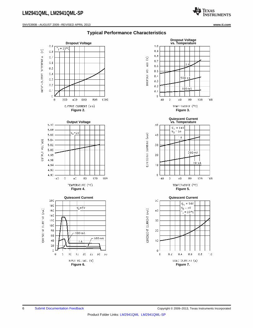
Typical Performance Characteristics
Dropout VoltageDropout Voltage vs. Temperature
Figure 2. Figure 3.
Quiescent CurrentOutput Voltage vs. Temperature
Figure 4. Figure 5.
Quiescent Current Quiescent Current
Figure 6. Figure 7.
6 Submit Documentation Feedback Copyright © 2009–2013, Texas Instruments Incorporated
Product Folder Links: LM2941QML LM2941QML-SP
LM2941QML, LM2941QML-SP
www.ti.com SNVS390B –AUGUST 2009–REVISED APRIL 2013
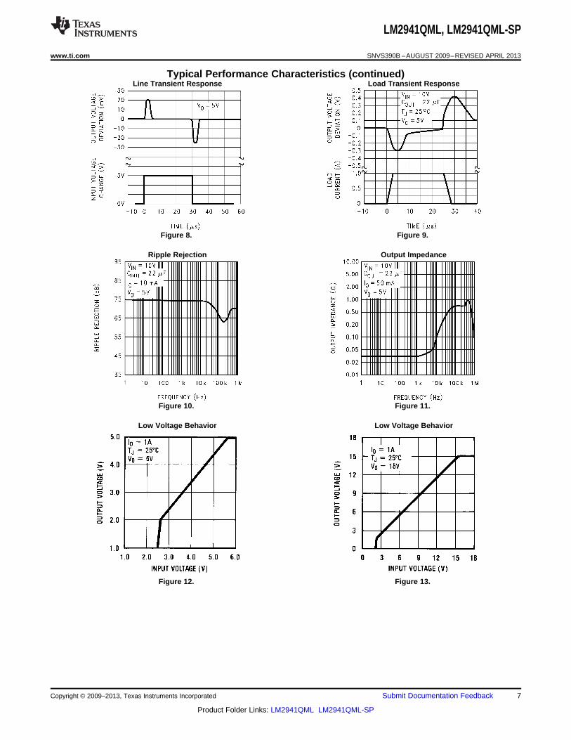
Typical Performance Characteristics (continued)Line Transient Response Load Transient Response
Figure 8. Figure 9.
Ripple Rejection Output Impedance
Figure 10. Figure 11.
Low Voltage Behavior Low Voltage Behavior
Figure 12. Figure 13.
Copyright © 2009–2013, Texas Instruments Incorporated Submit Documentation Feedback 7
Product Folder Links: LM2941QML LM2941QML-SP
LM2941QML, LM2941QML-SP
SNVS390B –AUGUST 2009–REVISED APRIL 2013 www.ti.com
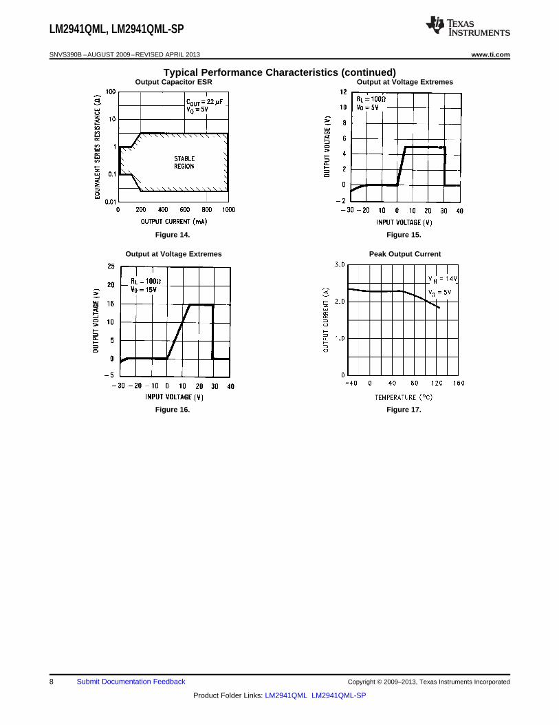
Typical Performance Characteristics (continued)Output Capacitor ESR Output at Voltage Extremes
Figure 14. Figure 15.
Output at Voltage Extremes Peak Output Current
Figure 16. Figure 17.
8 Submit Documentation Feedback Copyright © 2009–2013, Texas Instruments Incorporated
Product Folder Links: LM2941QML LM2941QML-SP
LM2941QML, LM2941QML-SP
www.ti.com SNVS390B –AUGUST 2009–REVISED APRIL 2013
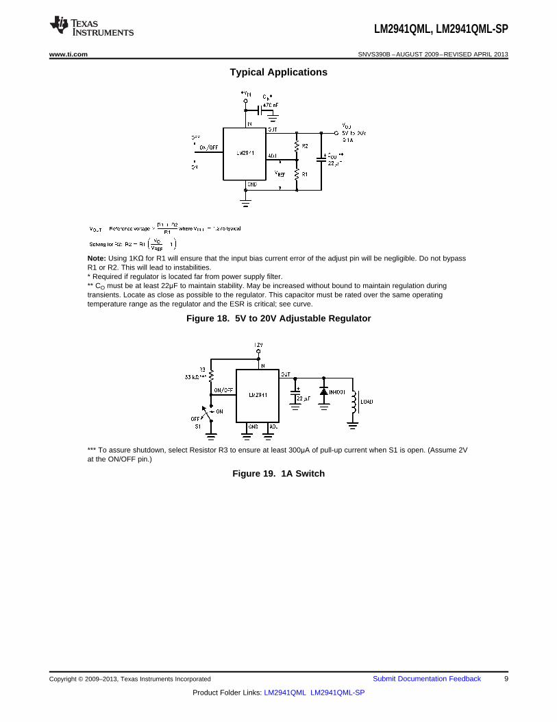
Typical Applications
Note: Using 1KΩ for R1 will ensure that the input bias current error of the adjust pin will be negligible. Do not bypassR1 or R2. This will lead to instabilities.* Required if regulator is located far from power supply filter.** CO must be at least 22μF to maintain stability. May be increased without bound to maintain regulation duringtransients. Locate as close as possible to the regulator. This capacitor must be rated over the same operatingtemperature range as the regulator and the ESR is critical; see curve.
Figure 18. 5V to 20V Adjustable Regulator
*** To assure shutdown, select Resistor R3 to ensure at least 300μA of pull-up current when S1 is open. (Assume 2Vat the ON/OFF pin.)
Figure 19. 1A Switch
Copyright © 2009–2013, Texas Instruments Incorporated Submit Documentation Feedback 9
Product Folder Links: LM2941QML LM2941QML-SP
LM2941QML, LM2941QML-SP
SNVS390B –AUGUST 2009–REVISED APRIL 2013 www.ti.com
REVISION HISTORY SECTION
Released Revision Section Changes
1 MDS data sheet converted into one Corp. data08/25/09 A New Release, Corporate format sheet format. Added Radiation products to ordering
table. MNLM2941-X Rev 4A1 will be archived.
Ordering Information — Added LM2941GW/883,LM2941GW-QMLV and LM2941GWRLQMLV.
12–Oct-2011 B Ordering Information, Absolute Max Ratings Absolute Max — Added Theta JA and Theta JC alongwith Package weight of 'GW' devices.RatingsLM2941QML Rev A will be archived.
10 Submit Documentation Feedback Copyright © 2009–2013, Texas Instruments Incorporated
Product Folder Links: LM2941QML LM2941QML-SP
LM2941QML, LM2941QML-SP
www.ti.com SNVS390B –AUGUST 2009–REVISED APRIL 2013
REVISION HISTORY
Changes from Revision A (April 2013) to Revision B Page
• Changed layout of National Data Sheet to TI format ............................................................................................................ 9
Copyright © 2009–2013, Texas Instruments Incorporated Submit Documentation Feedback 11
Product Folder Links: LM2941QML LM2941QML-SP
PACKAGE OPTION ADDENDUM
www.ti.com 25-Apr-2017
Addendum-Page 1
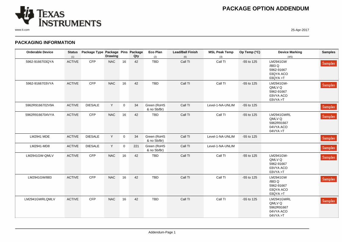
PACKAGING INFORMATION
Orderable Device Status(1)
Package Type PackageDrawing
Pins PackageQty
Eco Plan(2)
Lead/Ball Finish(6)
MSL Peak Temp(3)
Op Temp (°C) Device Marking(4/5)
Samples
5962-9166703QYA ACTIVE CFP NAC 16 42 TBD Call TI Call TI -55 to 125 LM2941GW/883 Q5962-9166703QYA ACO03QYA >T
5962-9166703VYA ACTIVE CFP NAC 16 42 TBD Call TI Call TI -55 to 125 LM2941GW-QMLV Q5962-9166703VYA ACO03VYA >T
5962R9166702V9A ACTIVE DIESALE Y 0 34 Green (RoHS& no Sb/Br)
Call TI Level-1-NA-UNLIM -55 to 125
5962R9166704VYA ACTIVE CFP NAC 16 42 TBD Call TI Call TI -55 to 125 LM2941GWRLQMLV Q5962R9166704VYA ACO04VYA >T
LM2941 MDE ACTIVE DIESALE Y 0 34 Green (RoHS& no Sb/Br)
Call TI Level-1-NA-UNLIM -55 to 125
LM2941-MD8 ACTIVE DIESALE Y 0 221 Green (RoHS& no Sb/Br)
Call TI Level-1-NA-UNLIM
LM2941GW-QMLV ACTIVE CFP NAC 16 42 TBD Call TI Call TI -55 to 125 LM2941GW-QMLV Q5962-9166703VYA ACO03VYA >T
LM2941GW/883 ACTIVE CFP NAC 16 42 TBD Call TI Call TI -55 to 125 LM2941GW/883 Q5962-9166703QYA ACO03QYA >T
LM2941GWRLQMLV ACTIVE CFP NAC 16 42 TBD Call TI Call TI -55 to 125 LM2941GWRLQMLV Q5962R9166704VYA ACO04VYA >T
PACKAGE OPTION ADDENDUM
www.ti.com 25-Apr-2017
Addendum-Page 2
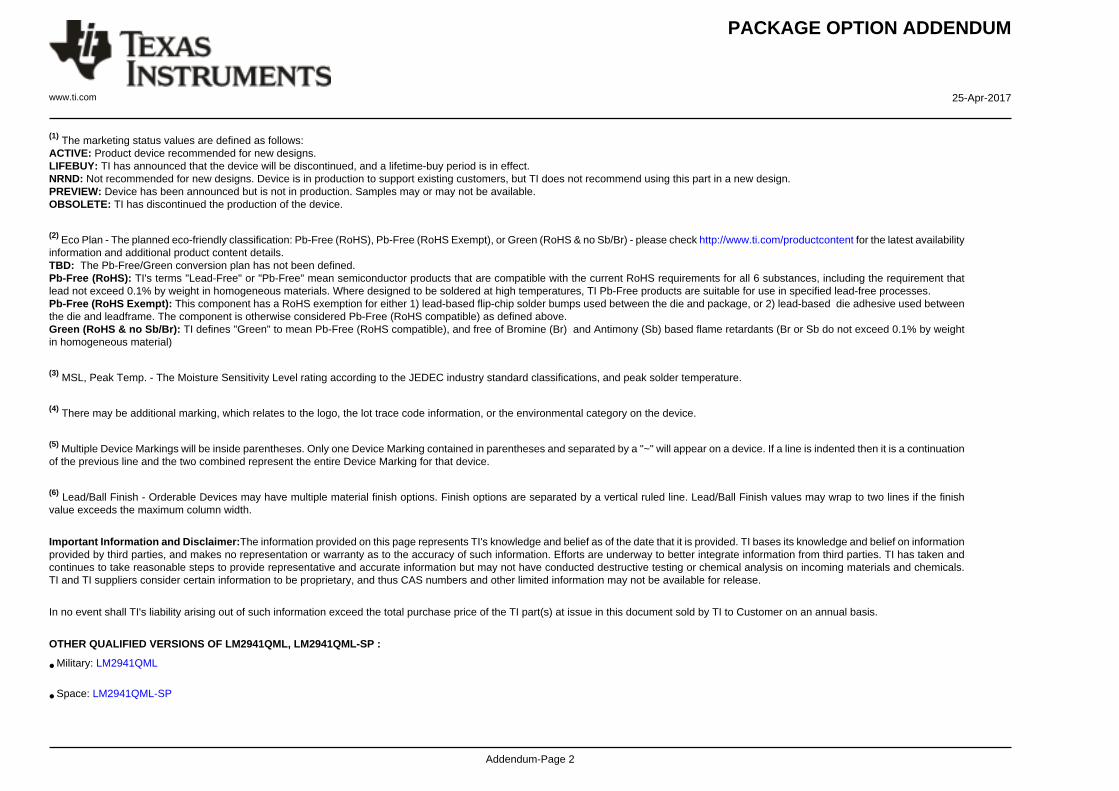
(1) The marketing status values are defined as follows:ACTIVE: Product device recommended for new designs.LIFEBUY: TI has announced that the device will be discontinued, and a lifetime-buy period is in effect.NRND: Not recommended for new designs. Device is in production to support existing customers, but TI does not recommend using this part in a new design.PREVIEW: Device has been announced but is not in production. Samples may or may not be available.OBSOLETE: TI has discontinued the production of the device.
(2) Eco Plan - The planned eco-friendly classification: Pb-Free (RoHS), Pb-Free (RoHS Exempt), or Green (RoHS & no Sb/Br) - please check http://www.ti.com/productcontent for the latest availabilityinformation and additional product content details.TBD: The Pb-Free/Green conversion plan has not been defined.Pb-Free (RoHS): TI's terms "Lead-Free" or "Pb-Free" mean semiconductor products that are compatible with the current RoHS requirements for all 6 substances, including the requirement thatlead not exceed 0.1% by weight in homogeneous materials. Where designed to be soldered at high temperatures, TI Pb-Free products are suitable for use in specified lead-free processes.Pb-Free (RoHS Exempt): This component has a RoHS exemption for either 1) lead-based flip-chip solder bumps used between the die and package, or 2) lead-based die adhesive used betweenthe die and leadframe. The component is otherwise considered Pb-Free (RoHS compatible) as defined above.Green (RoHS & no Sb/Br): TI defines "Green" to mean Pb-Free (RoHS compatible), and free of Bromine (Br) and Antimony (Sb) based flame retardants (Br or Sb do not exceed 0.1% by weightin homogeneous material)
(3) MSL, Peak Temp. - The Moisture Sensitivity Level rating according to the JEDEC industry standard classifications, and peak solder temperature.
(4) There may be additional marking, which relates to the logo, the lot trace code information, or the environmental category on the device.
(5) Multiple Device Markings will be inside parentheses. Only one Device Marking contained in parentheses and separated by a "~" will appear on a device. If a line is indented then it is a continuationof the previous line and the two combined represent the entire Device Marking for that device.
(6) Lead/Ball Finish - Orderable Devices may have multiple material finish options. Finish options are separated by a vertical ruled line. Lead/Ball Finish values may wrap to two lines if the finishvalue exceeds the maximum column width.
Important Information and Disclaimer:The information provided on this page represents TI's knowledge and belief as of the date that it is provided. TI bases its knowledge and belief on informationprovided by third parties, and makes no representation or warranty as to the accuracy of such information. Efforts are underway to better integrate information from third parties. TI has taken andcontinues to take reasonable steps to provide representative and accurate information but may not have conducted destructive testing or chemical analysis on incoming materials and chemicals.TI and TI suppliers consider certain information to be proprietary, and thus CAS numbers and other limited information may not be available for release.
In no event shall TI's liability arising out of such information exceed the total purchase price of the TI part(s) at issue in this document sold by TI to Customer on an annual basis.
OTHER QUALIFIED VERSIONS OF LM2941QML, LM2941QML-SP :
• Military: LM2941QML
• Space: LM2941QML-SP
PACKAGE OPTION ADDENDUM
www.ti.com 25-Apr-2017
Addendum-Page 3
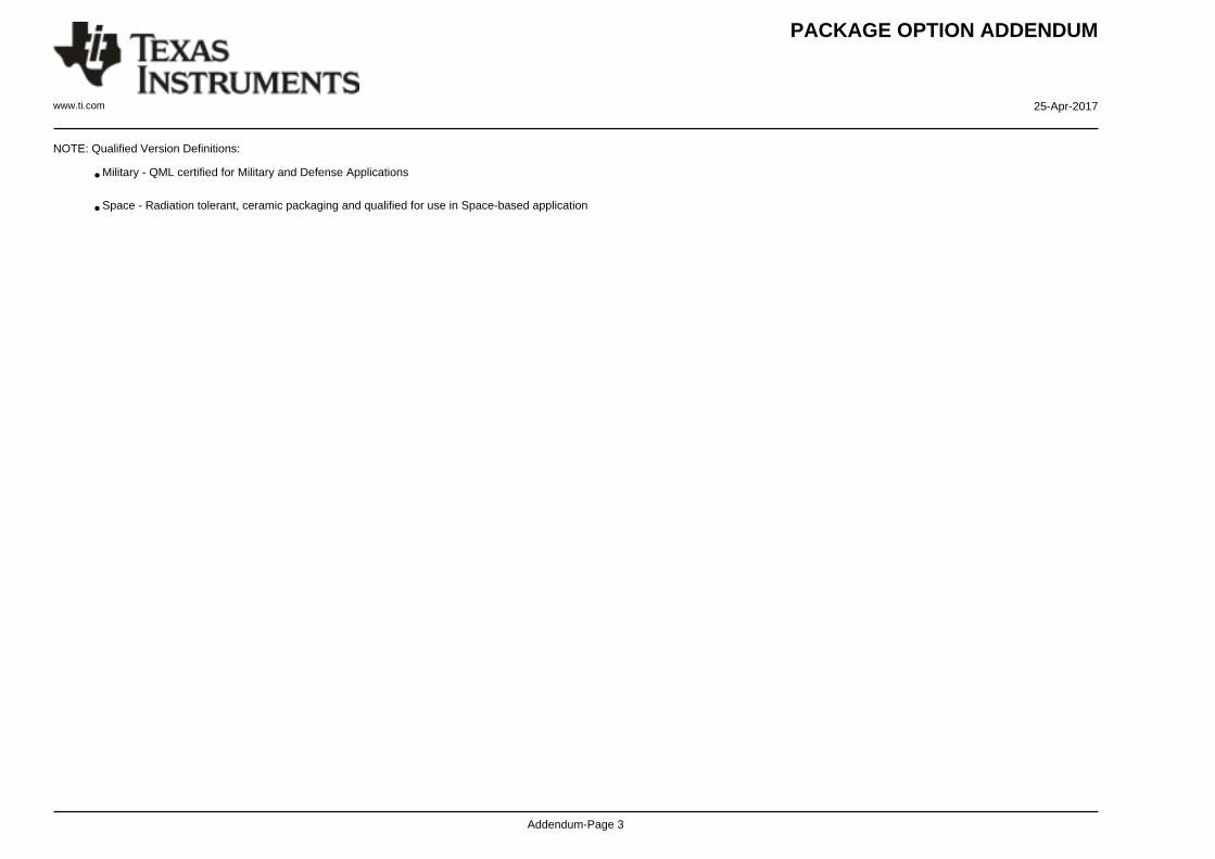
NOTE: Qualified Version Definitions:
• Military - QML certified for Military and Defense Applications
• Space - Radiation tolerant, ceramic packaging and qualified for use in Space-based application
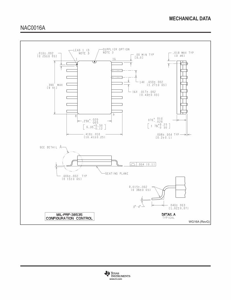
MECHANICAL DATA
NAC0016A
www.ti.com
WG16A (RevG)
IMPORTANT NOTICE
Texas Instruments Incorporated (TI) reserves the right to make corrections, enhancements, improvements and other changes to itssemiconductor products and services per JESD46, latest issue, and to discontinue any product or service per JESD48, latest issue. Buyersshould obtain the latest relevant information before placing orders and should verify that such information is current and complete.TI’s published terms of sale for semiconductor products (http://www.ti.com/sc/docs/stdterms.htm) apply to the sale of packaged integratedcircuit products that TI has qualified and released to market. Additional terms may apply to the use or sale of other types of TI products andservices.Reproduction of significant portions of TI information in TI data sheets is permissible only if reproduction is without alteration and isaccompanied by all associated warranties, conditions, limitations, and notices. TI is not responsible or liable for such reproduceddocumentation. Information of third parties may be subject to additional restrictions. Resale of TI products or services with statementsdifferent from or beyond the parameters stated by TI for that product or service voids all express and any implied warranties for theassociated TI product or service and is an unfair and deceptive business practice. TI is not responsible or liable for any such statements.Buyers and others who are developing systems that incorporate TI products (collectively, “Designers”) understand and agree that Designersremain responsible for using their independent analysis, evaluation and judgment in designing their applications and that Designers havefull and exclusive responsibility to assure the safety of Designers' applications and compliance of their applications (and of all TI productsused in or for Designers’ applications) with all applicable regulations, laws and other applicable requirements. Designer represents that, withrespect to their applications, Designer has all the necessary expertise to create and implement safeguards that (1) anticipate dangerousconsequences of failures, (2) monitor failures and their consequences, and (3) lessen the likelihood of failures that might cause harm andtake appropriate actions. Designer agrees that prior to using or distributing any applications that include TI products, Designer willthoroughly test such applications and the functionality of such TI products as used in such applications.TI’s provision of technical, application or other design advice, quality characterization, reliability data or other services or information,including, but not limited to, reference designs and materials relating to evaluation modules, (collectively, “TI Resources”) are intended toassist designers who are developing applications that incorporate TI products; by downloading, accessing or using TI Resources in anyway, Designer (individually or, if Designer is acting on behalf of a company, Designer’s company) agrees to use any particular TI Resourcesolely for this purpose and subject to the terms of this Notice.TI’s provision of TI Resources does not expand or otherwise alter TI’s applicable published warranties or warranty disclaimers for TIproducts, and no additional obligations or liabilities arise from TI providing such TI Resources. TI reserves the right to make corrections,enhancements, improvements and other changes to its TI Resources. TI has not conducted any testing other than that specificallydescribed in the published documentation for a particular TI Resource.Designer is authorized to use, copy and modify any individual TI Resource only in connection with the development of applications thatinclude the TI product(s) identified in such TI Resource. NO OTHER LICENSE, EXPRESS OR IMPLIED, BY ESTOPPEL OR OTHERWISETO ANY OTHER TI INTELLECTUAL PROPERTY RIGHT, AND NO LICENSE TO ANY TECHNOLOGY OR INTELLECTUAL PROPERTYRIGHT OF TI OR ANY THIRD PARTY IS GRANTED HEREIN, including but not limited to any patent right, copyright, mask work right, orother intellectual property right relating to any combination, machine, or process in which TI products or services are used. Informationregarding or referencing third-party products or services does not constitute a license to use such products or services, or a warranty orendorsement thereof. Use of TI Resources may require a license from a third party under the patents or other intellectual property of thethird party, or a license from TI under the patents or other intellectual property of TI.TI RESOURCES ARE PROVIDED “AS IS” AND WITH ALL FAULTS. TI DISCLAIMS ALL OTHER WARRANTIES ORREPRESENTATIONS, EXPRESS OR IMPLIED, REGARDING RESOURCES OR USE THEREOF, INCLUDING BUT NOT LIMITED TOACCURACY OR COMPLETENESS, TITLE, ANY EPIDEMIC FAILURE WARRANTY AND ANY IMPLIED WARRANTIES OFMERCHANTABILITY, FITNESS FOR A PARTICULAR PURPOSE, AND NON-INFRINGEMENT OF ANY THIRD PARTY INTELLECTUALPROPERTY RIGHTS. TI SHALL NOT BE LIABLE FOR AND SHALL NOT DEFEND OR INDEMNIFY DESIGNER AGAINST ANY CLAIM,INCLUDING BUT NOT LIMITED TO ANY INFRINGEMENT CLAIM THAT RELATES TO OR IS BASED ON ANY COMBINATION OFPRODUCTS EVEN IF DESCRIBED IN TI RESOURCES OR OTHERWISE. IN NO EVENT SHALL TI BE LIABLE FOR ANY ACTUAL,DIRECT, SPECIAL, COLLATERAL, INDIRECT, PUNITIVE, INCIDENTAL, CONSEQUENTIAL OR EXEMPLARY DAMAGES INCONNECTION WITH OR ARISING OUT OF TI RESOURCES OR USE THEREOF, AND REGARDLESS OF WHETHER TI HAS BEENADVISED OF THE POSSIBILITY OF SUCH DAMAGES.Unless TI has explicitly designated an individual product as meeting the requirements of a particular industry standard (e.g., ISO/TS 16949and ISO 26262), TI is not responsible for any failure to meet such industry standard requirements.Where TI specifically promotes products as facilitating functional safety or as compliant with industry functional safety standards, suchproducts are intended to help enable customers to design and create their own applications that meet applicable functional safety standardsand requirements. Using products in an application does not by itself establish any safety features in the application. Designers mustensure compliance with safety-related requirements and standards applicable to their applications. Designer may not use any TI products inlife-critical medical equipment unless authorized officers of the parties have executed a special contract specifically governing such use.Life-critical medical equipment is medical equipment where failure of such equipment would cause serious bodily injury or death (e.g., lifesupport, pacemakers, defibrillators, heart pumps, neurostimulators, and implantables). Such equipment includes, without limitation, allmedical devices identified by the U.S. Food and Drug Administration as Class III devices and equivalent classifications outside the U.S.TI may expressly designate certain products as completing a particular qualification (e.g., Q100, Military Grade, or Enhanced Product).Designers agree that it has the necessary expertise to select the product with the appropriate qualification designation for their applicationsand that proper product selection is at Designers’ own risk. Designers are solely responsible for compliance with all legal and regulatoryrequirements in connection with such selection.Designer will fully indemnify TI and its representatives against any damages, costs, losses, and/or liabilities arising out of Designer’s non-compliance with the terms and provisions of this Notice.
Mailing Address: Texas Instruments, Post Office Box 655303, Dallas, Texas 75265Copyright © 2017, Texas Instruments Incorporated