Embed Size (px)
Citation preview
LM2931-N
www.ti.com SNOSBE5G –MARCH 2000–REVISED APRIL 2013
LM2931-N Series Low Dropout RegulatorsCheck for Samples: LM2931-N
1FEATURES DESCRIPTIONThe LM2931-N positive voltage regulator features a
2• Very Low Quiescent Currentvery low quiescent current of 1mA or less when
• Output Current in Excess of 100 mA supplying 10mA loads. This unique characteristic and• Input-output Differential Less than 0.6V the extremely low input-output differential required for
proper regulation (0.2V for output currents of 10mA)• Reverse Battery Protectionmake the LM2931-N the ideal regulator for standby• 60V Load Dump Protection power systems. Applications include memory standby
• −50V Reverse Transient Protection circuits, CMOS and other low power processor powersupplies as well as systems demanding as much as• Short Circuit Protection100mA of output current.• Internal Thermal Overload ProtectionDesigned originally for automotive applications, the• Mirror-image Insertion ProtectionLM2931-N and all regulated circuitry are protected• Available in TO-220, TO-92, TO-263, or SOIC-8 from reverse battery installations or 2 battery jumps.
Packages During line transients, such as a load dump (60V)• Available as Adjustable with TTL Compatible when the input voltage to the regulator can
Switch momentarily exceed the specified maximumoperating voltage, the regulator will automatically shutdown to protect both internal circuits and the load.The LM2931-N cannot be harmed by temporarymirror-image insertion. Familiar regulator featuressuch as short circuit and thermal overload protectionare also provided.
The LM2931-N family includes a fixed 5V output(±3.8% tolerance for A grade) or an adjustable outputwith ON/OFF pin. Both versions are available in aTO-220 power package, DDPAK/TO-263 surfacemount package, and an 8-lead SOIC package. Thefixed output version is also available in the TO-92plastic package.
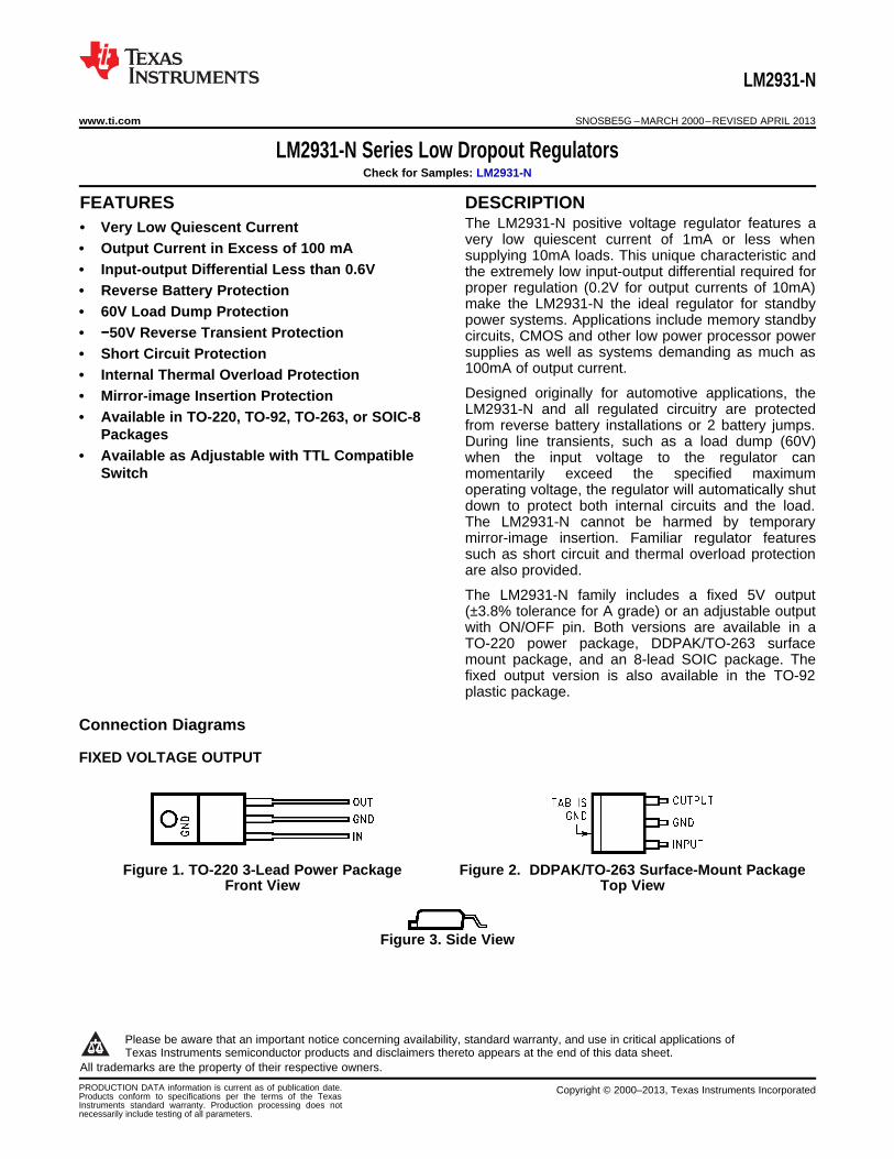
Connection Diagrams
FIXED VOLTAGE OUTPUT
Figure 1. TO-220 3-Lead Power Package Figure 2. DDPAK/TO-263 Surface-Mount PackageFront View Top View
Figure 3. Side View
1
Please be aware that an important notice concerning availability, standard warranty, and use in critical applications ofTexas Instruments semiconductor products and disclaimers thereto appears at the end of this data sheet.
2All trademarks are the property of their respective owners.
PRODUCTION DATA information is current as of publication date. Copyright © 2000–2013, Texas Instruments IncorporatedProducts conform to specifications per the terms of the TexasInstruments standard warranty. Production processing does notnecessarily include testing of all parameters.
LM2931-N
SNOSBE5G –MARCH 2000–REVISED APRIL 2013 www.ti.com
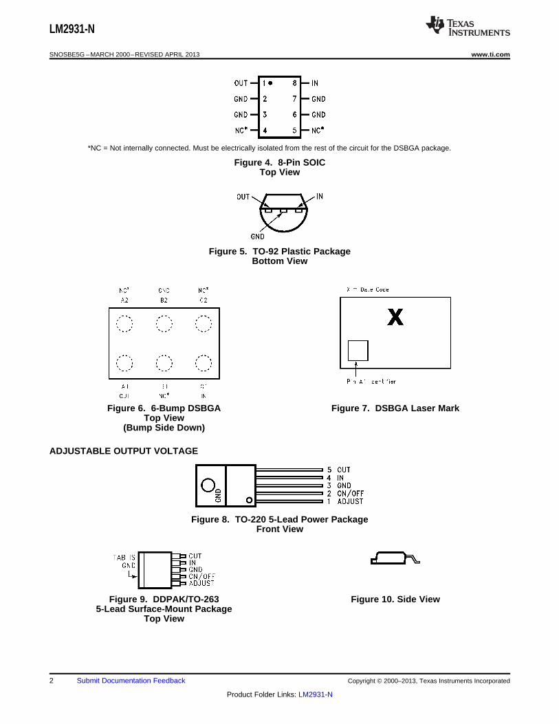
*NC = Not internally connected. Must be electrically isolated from the rest of the circuit for the DSBGA package.
Figure 4. 8-Pin SOICTop View
Figure 5. TO-92 Plastic PackageBottom View
Figure 6. 6-Bump DSBGA Figure 7. DSBGA Laser MarkTop View
(Bump Side Down)
ADJUSTABLE OUTPUT VOLTAGE
Figure 8. TO-220 5-Lead Power PackageFront View
Figure 9. DDPAK/TO-263 Figure 10. Side View5-Lead Surface-Mount Package
Top View
2 Submit Documentation Feedback Copyright © 2000–2013, Texas Instruments Incorporated
Product Folder Links: LM2931-N
LM2931-N
www.ti.com SNOSBE5G –MARCH 2000–REVISED APRIL 2013
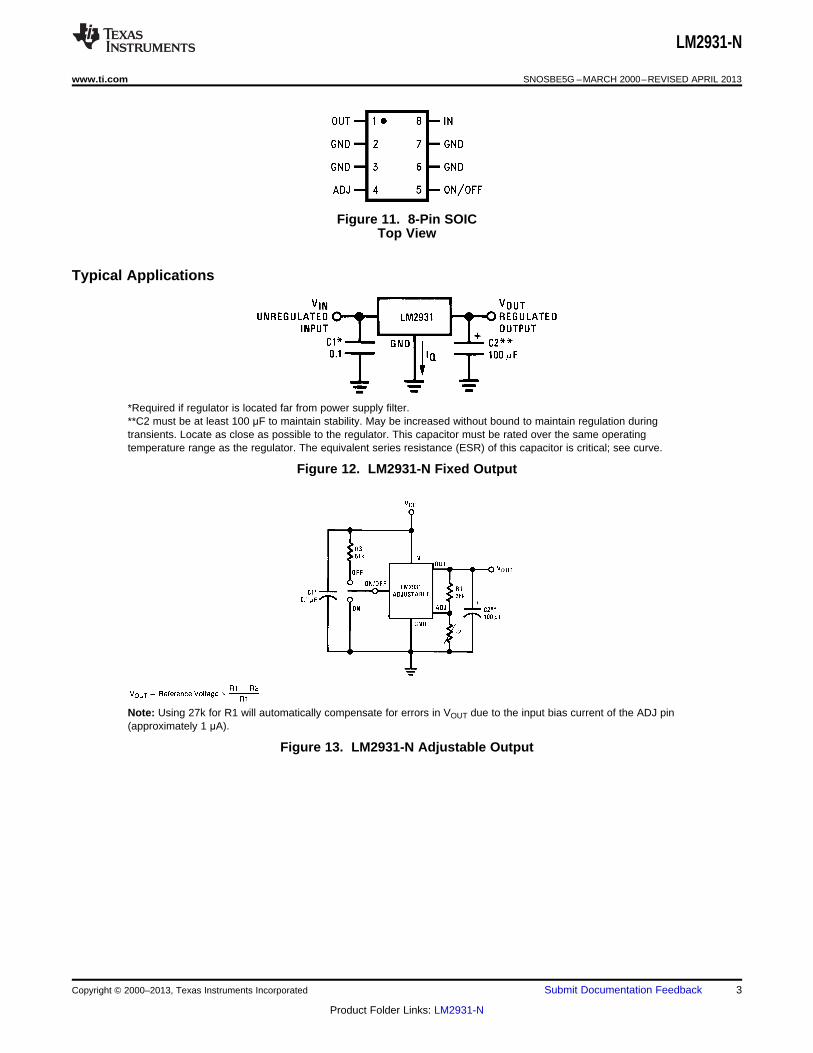
Figure 11. 8-Pin SOICTop View
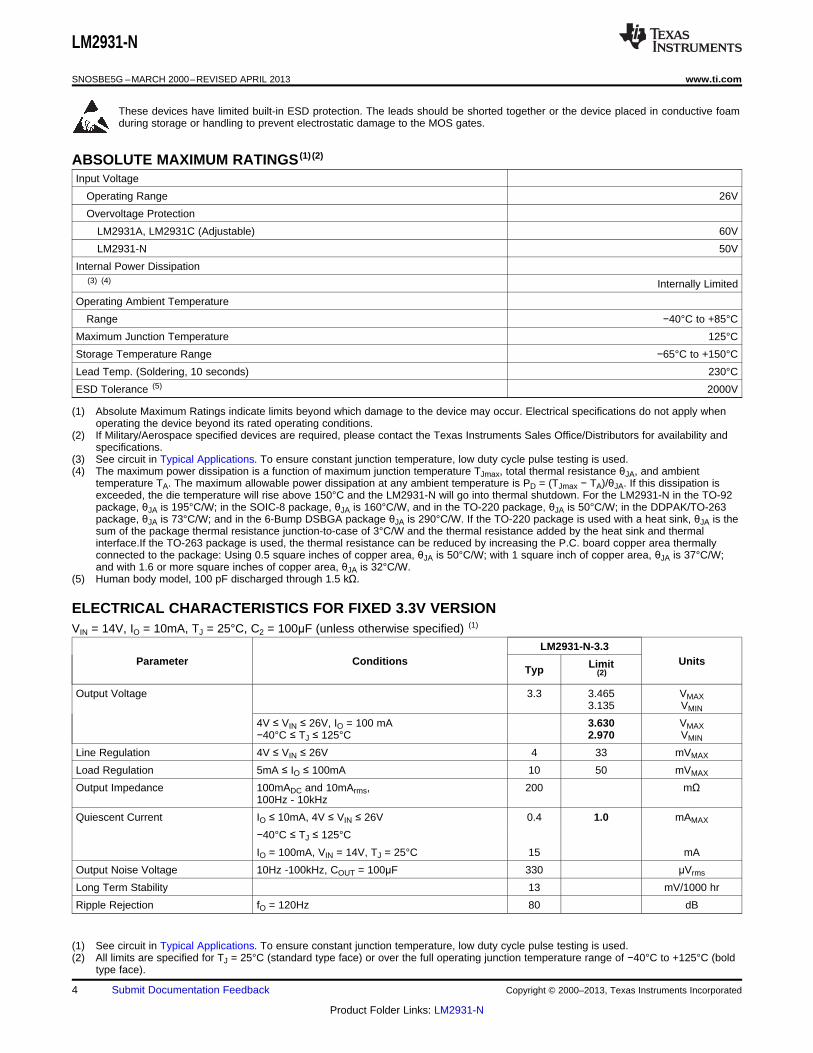
Typical Applications
*Required if regulator is located far from power supply filter.**C2 must be at least 100 μF to maintain stability. May be increased without bound to maintain regulation duringtransients. Locate as close as possible to the regulator. This capacitor must be rated over the same operatingtemperature range as the regulator. The equivalent series resistance (ESR) of this capacitor is critical; see curve.
Figure 12. LM2931-N Fixed Output
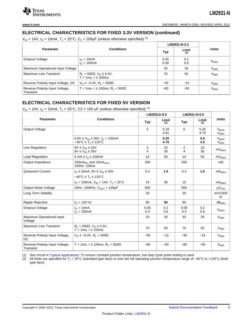
Note: Using 27k for R1 will automatically compensate for errors in VOUT due to the input bias current of the ADJ pin(approximately 1 μA).
Figure 13. LM2931-N Adjustable Output
Copyright © 2000–2013, Texas Instruments Incorporated Submit Documentation Feedback 3
Product Folder Links: LM2931-N
LM2931-N
SNOSBE5G –MARCH 2000–REVISED APRIL 2013 www.ti.com
These devices have limited built-in ESD protection. The leads should be shorted together or the device placed in conductive foamduring storage or handling to prevent electrostatic damage to the MOS gates.
ABSOLUTE MAXIMUM RATINGS (1) (2)
Input Voltage
Operating Range 26V
Overvoltage Protection
LM2931A, LM2931C (Adjustable) 60V
LM2931-N 50V
Internal Power Dissipation(3) (4) Internally Limited
Operating Ambient Temperature
Range −40°C to +85°C
Maximum Junction Temperature 125°C
Storage Temperature Range −65°C to +150°C
Lead Temp. (Soldering, 10 seconds) 230°C
ESD Tolerance (5) 2000V
(1) Absolute Maximum Ratings indicate limits beyond which damage to the device may occur. Electrical specifications do not apply whenoperating the device beyond its rated operating conditions.
(2) If Military/Aerospace specified devices are required, please contact the Texas Instruments Sales Office/Distributors for availability andspecifications.
(3) See circuit in Typical Applications. To ensure constant junction temperature, low duty cycle pulse testing is used.(4) The maximum power dissipation is a function of maximum junction temperature TJmax, total thermal resistance θJA, and ambient
temperature TA. The maximum allowable power dissipation at any ambient temperature is PD = (TJmax − TA)/θJA. If this dissipation isexceeded, the die temperature will rise above 150°C and the LM2931-N will go into thermal shutdown. For the LM2931-N in the TO-92package, θJA is 195°C/W; in the SOIC-8 package, θJA is 160°C/W, and in the TO-220 package, θJA is 50°C/W; in the DDPAK/TO-263package, θJA is 73°C/W; and in the 6-Bump DSBGA package θJA is 290°C/W. If the TO-220 package is used with a heat sink, θJA is thesum of the package thermal resistance junction-to-case of 3°C/W and the thermal resistance added by the heat sink and thermalinterface.If the TO-263 package is used, the thermal resistance can be reduced by increasing the P.C. board copper area thermallyconnected to the package: Using 0.5 square inches of copper area, θJA is 50°C/W; with 1 square inch of copper area, θJA is 37°C/W;and with 1.6 or more square inches of copper area, θJA is 32°C/W.
(5) Human body model, 100 pF discharged through 1.5 kΩ.
ELECTRICAL CHARACTERISTICS FOR FIXED 3.3V VERSIONVIN = 14V, IO = 10mA, TJ = 25°C, C2 = 100μF (unless otherwise specified) (1)
LM2931-N-3.3Parameter Conditions UnitsLimitTyp (2)
Output Voltage 3.3 3.465 VMAX3.135 VMIN
4V ≤ VIN ≤ 26V, IO = 100 mA 3.630 VMAX−40°C ≤ TJ ≤ 125°C 2.970 VMIN
Line Regulation 4V ≤ VIN ≤ 26V 4 33 mVMAX
Load Regulation 5mA ≤ IO ≤ 100mA 10 50 mVMAX
Output Impedance 100mADC and 10mArms, 200 mΩ100Hz - 10kHz
Quiescent Current IO ≤ 10mA, 4V ≤ VIN ≤ 26V 0.4 1.0 mAMAX
−40°C ≤ TJ ≤ 125°C
IO = 100mA, VIN = 14V, TJ = 25°C 15 mA
Output Noise Voltage 10Hz -100kHz, COUT = 100μF 330 μVrms
Long Term Stability 13 mV/1000 hr
Ripple Rejection fO = 120Hz 80 dB
(1) See circuit in Typical Applications. To ensure constant junction temperature, low duty cycle pulse testing is used.(2) All limits are specified for TJ = 25°C (standard type face) or over the full operating junction temperature range of −40°C to +125°C (bold
type face).
4 Submit Documentation Feedback Copyright © 2000–2013, Texas Instruments Incorporated
Product Folder Links: LM2931-N
LM2931-N
www.ti.com SNOSBE5G –MARCH 2000–REVISED APRIL 2013
ELECTRICAL CHARACTERISTICS FOR FIXED 3.3V VERSION (continued)VIN = 14V, IO = 10mA, TJ = 25°C, C2 = 100μF (unless otherwise specified) (1)
LM2931-N-3.3Parameter Conditions UnitsLimitTyp (2)
Dropout Voltage IO = 10mA 0.05 0.2 VMAXIO = 100mA 0.30 0.6
Maximum Operational Input Voltage 33 26 VMIN
Maximum Line Transient RL = 500Ω, VO ≤ 5.5V, 70 50 VMINT = 1ms, τ ≤ 100ms
Reverse Polarity Input Voltage, DC VO ≥ −0.3V, RL = 500Ω −30 −15 VMIN
Reverse Polarity Input Voltage, T = 1ms, τ ≤ 100ms, RL = 500Ω −80 −50 VMINTransient
ELECTRICAL CHARACTERISTICS FOR FIXED 5V VERSIONVIN = 14V, IO = 10mA, TJ = 25°C, C2 = 100 μF (unless otherwise specified) (1)
LM2931A-5.0 LM2931-N-5.0Parameter Conditions UnitsLimit LimitTyp Typ(2) (2)
Output Voltage 5 5.19 5 5.25 VMAX4.81 4.75 VMIN
6.0V ≤ VIN ≤ 26V, IO = 100mA 5.25 5.5 VMAX−40°C ≤ TJ ≤ 125°C 4.75 4.5 VMIN
Line Regulation 9V ≤ VIN ≤ 16V 2 10 2 10 mVMAX6V ≤ VIN ≤ 26V 4 30 4 30
Load Regulation 5 mA ≤ IO ≤ 100mA 14 50 14 50 mVMAX
Output Impedance 100mADC and 10mArms, 200 200 mΩ100Hz -10kHz
Quiescent Current IO ≤ 10mA, 6V ≤ VIN ≤ 26V 0.4 1.0 0.4 1.0 mAMAX
−40°C ≤ TJ ≤ 125°C
IO = 100mA, VIN = 14V, TJ = 25°C 15 30 15 mAMAX
Output Noise Voltage 10Hz -100kHz, COUT = 100μF 500 500 μVrms
Long Term Stability 20 20 mV/1000hr
Ripple Rejection fO = 120 Hz 80 55 80 dBMIN
Dropout Voltage IO = 10mA 0.05 0.2 0.05 0.2 VMAXIO = 100mA 0.3 0.6 0.3 0.6
Maximum Operational Input 33 26 33 26 VMINVoltage
Maximum Line Transient RL = 500Ω, VO ≤ 5.5V, 70 60 70 50 VMINT = 1ms, τ ≤ 100ms
Reverse Polarity Input Voltage, VO ≥ −0.3V, RL = 500Ω −30 −15 −30 −15 VMINDC
Reverse Polarity Input Voltage, T = 1ms, τ ≤ 100ms, RL = 500Ω −80 −50 −80 −50 VMINTransient
(1) See circuit in Typical Applications. To ensure constant junction temperature, low duty cycle pulse testing is used.(2) All limits are specified for TJ = 25°C (standard type face) or over the full operating junction temperature range of −40°C to +125°C (bold
type face).
Copyright © 2000–2013, Texas Instruments Incorporated Submit Documentation Feedback 5
Product Folder Links: LM2931-N
LM2931-N
SNOSBE5G –MARCH 2000–REVISED APRIL 2013 www.ti.com
ELECTRICAL CHARACTERISTICS FOR ADJUSTABLE VERSIONVIN = 14V, VOUT = 3V, IO = 10 mA, TJ = 25°C, R1 = 27k, C2 = 100 μF (unless otherwise specified) (1)
Parameter Conditions Typ Limit Units Limit
Reference Voltage 1.20 1.26 VMAX
1.14 VMIN
IO ≤ 100 mA, −40°C ≤ Tj ≤ 125°C, R1 = 27k 1.32 VMAX
Measured from VOUT to Adjust Pin 1.08 VMIN
Output Voltage Range 24 VMAX
3 VMIN
Line Regulation VOUT + 0.6V ≤ VIN ≤ 26V 0.2 1.5 mV/VMAX
Load Regulation 5 mA ≤ IO ≤ 100 mA 0.3 1 %MAX
Output Impedance 100 mADC and 10 mArms, 100 Hz–10 kHz 40 mΩ/V
Quiescent Current IO = 10 mA 0.4 1 mAMAX
IO = 100 mA 15 mA
During Shutdown RL = 500Ω 0.8 1 mAMAX
Output Noise Voltage 10 Hz–100 kHz 100 μVrms/V
Long Term Stability 0.4 %/1000 hr
Ripple Rejection fO = 120 Hz 0.02 %/V
Dropout Voltage IO ≤ 10 mA 0.05 0.2 VMAX
IO = 100 mA 0.3 0.6 VMAX
Maximum Operational Input
Voltage 33 26 VMIN
Maximum Line Transient IO = 10 mA, Reference Voltage ≤ 1.5V 70 60 VMIN
T = 1 ms, τ ≤ 100 ms
Reverse Polarity Input VO ≥ −0.3V, RL = 500ΩVoltage, DC −30 −15 VMIN
Reverse Polarity Input T = 1 ms, τ ≤ 100 ms, RL = 500ΩVoltage, Transient −80 −50 VMIN
On/Off Threshold Voltage VO=3V
On 2.0 1.2 VMAX
Off 2.2 3.25 VMIN
On/Off Threshold Current 20 50 μAMAX
(1) See circuit in Typical Applications. To ensure constant junction temperature, low duty cycle pulse testing is used.
6 Submit Documentation Feedback Copyright © 2000–2013, Texas Instruments Incorporated
Product Folder Links: LM2931-N
LM2931-N
www.ti.com SNOSBE5G –MARCH 2000–REVISED APRIL 2013
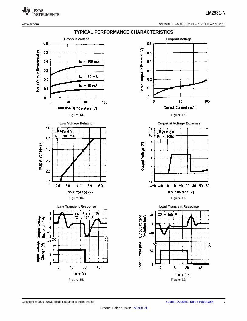
TYPICAL PERFORMANCE CHARACTERISTICS
Dropout Voltage Dropout Voltage
Figure 14. Figure 15.
Low Voltage Behavior Output at Voltage Extremes
Figure 16. Figure 17.
Line Transient Response Load Transient Response
Figure 18. Figure 19.
Copyright © 2000–2013, Texas Instruments Incorporated Submit Documentation Feedback 7
Product Folder Links: LM2931-N
LM2931-N
SNOSBE5G –MARCH 2000–REVISED APRIL 2013 www.ti.com
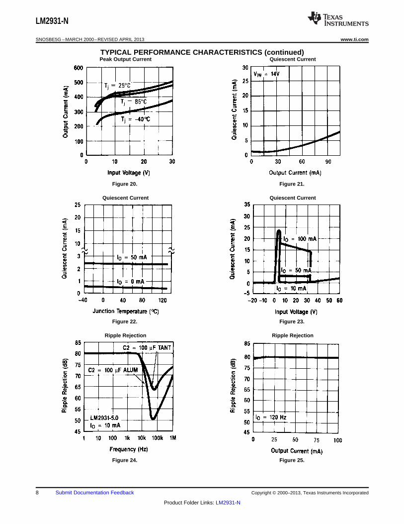
TYPICAL PERFORMANCE CHARACTERISTICS (continued)Peak Output Current Quiescent Current
Figure 20. Figure 21.
Quiescent Current Quiescent Current
Figure 22. Figure 23.
Ripple Rejection Ripple Rejection
Figure 24. Figure 25.
8 Submit Documentation Feedback Copyright © 2000–2013, Texas Instruments Incorporated
Product Folder Links: LM2931-N
LM2931-N
www.ti.com SNOSBE5G –MARCH 2000–REVISED APRIL 2013
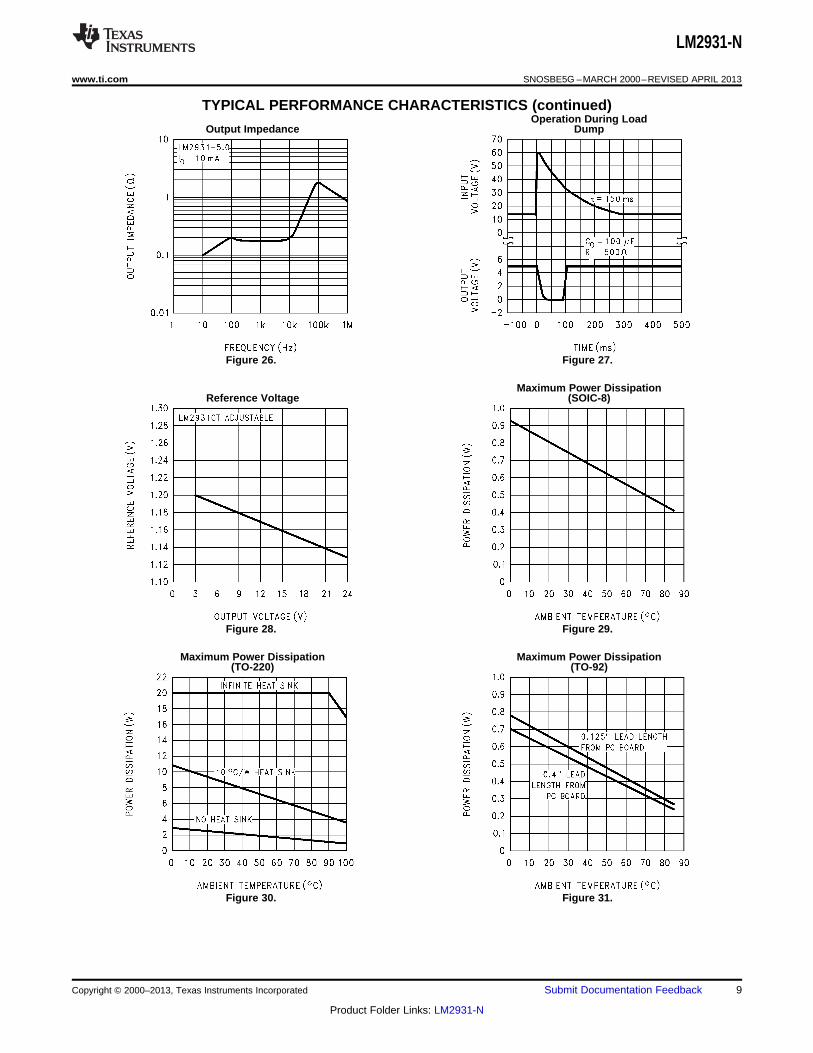
TYPICAL PERFORMANCE CHARACTERISTICS (continued)Operation During Load
Output Impedance Dump
Figure 26. Figure 27.
Maximum Power DissipationReference Voltage (SOIC-8)
Figure 28. Figure 29.
Maximum Power Dissipation Maximum Power Dissipation(TO-220) (TO-92)
Figure 30. Figure 31.
Copyright © 2000–2013, Texas Instruments Incorporated Submit Documentation Feedback 9
Product Folder Links: LM2931-N
LM2931-N
SNOSBE5G –MARCH 2000–REVISED APRIL 2013 www.ti.com
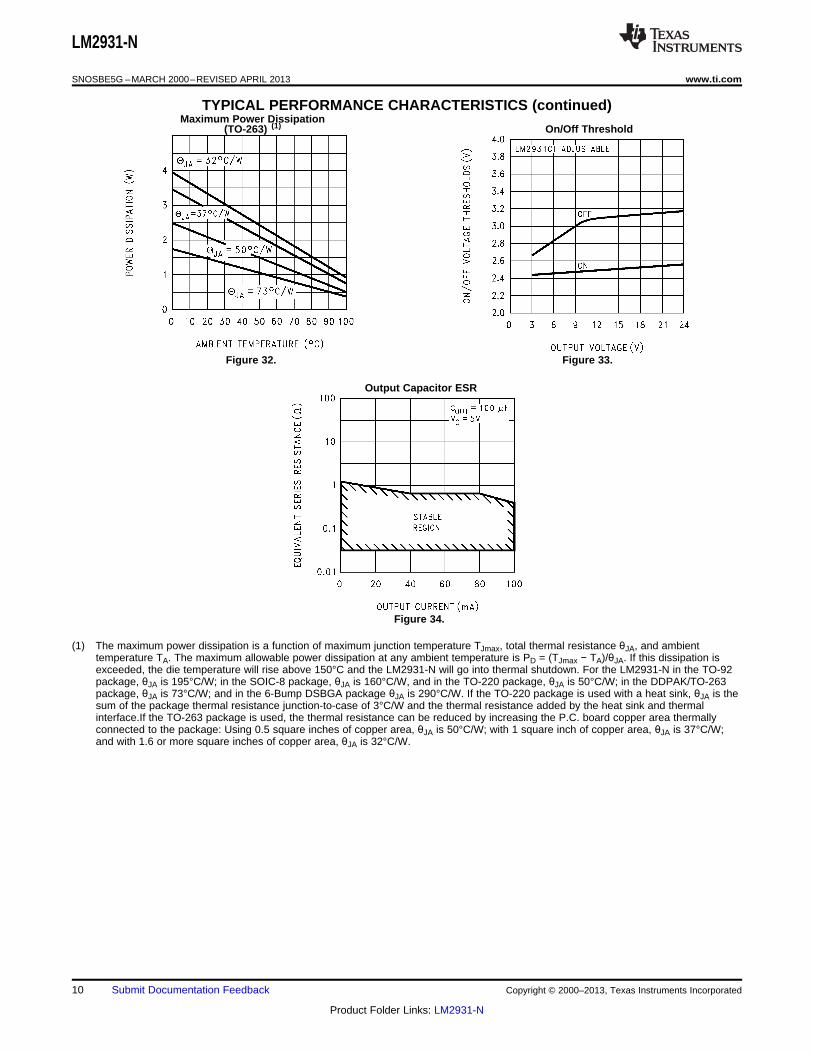
TYPICAL PERFORMANCE CHARACTERISTICS (continued)Maximum Power Dissipation
(TO-263) (1) On/Off Threshold
Figure 32. Figure 33.
Output Capacitor ESR
Figure 34.
(1) The maximum power dissipation is a function of maximum junction temperature TJmax, total thermal resistance θJA, and ambienttemperature TA. The maximum allowable power dissipation at any ambient temperature is PD = (TJmax − TA)/θJA. If this dissipation isexceeded, the die temperature will rise above 150°C and the LM2931-N will go into thermal shutdown. For the LM2931-N in the TO-92package, θJA is 195°C/W; in the SOIC-8 package, θJA is 160°C/W, and in the TO-220 package, θJA is 50°C/W; in the DDPAK/TO-263package, θJA is 73°C/W; and in the 6-Bump DSBGA package θJA is 290°C/W. If the TO-220 package is used with a heat sink, θJA is thesum of the package thermal resistance junction-to-case of 3°C/W and the thermal resistance added by the heat sink and thermalinterface.If the TO-263 package is used, the thermal resistance can be reduced by increasing the P.C. board copper area thermallyconnected to the package: Using 0.5 square inches of copper area, θJA is 50°C/W; with 1 square inch of copper area, θJA is 37°C/W;and with 1.6 or more square inches of copper area, θJA is 32°C/W.
10 Submit Documentation Feedback Copyright © 2000–2013, Texas Instruments Incorporated
Product Folder Links: LM2931-N
LM2931-N
www.ti.com SNOSBE5G –MARCH 2000–REVISED APRIL 2013
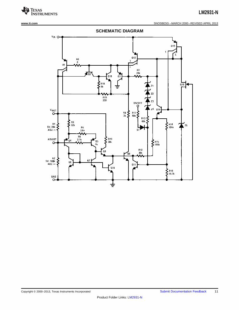
SCHEMATIC DIAGRAM
Copyright © 2000–2013, Texas Instruments Incorporated Submit Documentation Feedback 11
Product Folder Links: LM2931-N
LM2931-N
SNOSBE5G –MARCH 2000–REVISED APRIL 2013 www.ti.com
APPLICATION HINTS
One of the distinguishing factors of the LM2931-N series regulators is the requirement of an output capacitor fordevice stability. The value required varies greatly depending upon the application circuit and other factors. Thussome comments on the characteristics of both capacitors and the regulator are in order.
High frequency characteristics of electrolytic capacitors depend greatly on the type and even the manufacturer.As a result, a value of capacitance that works well with the LM2931-N for one brand or type may not necessarybe sufficient with an electrolytic of different origin. Sometimes actual bench testing, as described later, will be theonly means to determine the proper capacitor type and value. Experience has shown that, as a rule of thumb, themore expensive and higher quality electrolytics generally allow a smaller value for regulator stability. As anexample, while a high-quality 100 μF aluminum electrolytic covers all general application circuits, similar stabilitycan be obtained with a tantalum electrolytic of only 47μF. This factor of two can generally be applied to anyspecial application circuit also.
Another critical characteristic of electrolytics is their performance over temperature. While the LM2931-N isdesigned to operate to −40°C, the same is not always true with all electrolytics (hot is generally not a problem).The electrolyte in many aluminum types will freeze around −30°C, reducing their effective value to zero. Sincethe capacitance is needed for regulator stability, the natural result is oscillation (and lots of it) at the regulatoroutput. For all application circuits where cold operation is necessary, the output capacitor must be rated tooperate at the minimum temperature. By coincidence, worst-case stability for the LM2931-N also occurs atminimum temperatures. As a result, in applications where the regulator junction temperature will never be lessthan 25°C, the output capacitor can be reduced approximately by a factor of two over the value needed for theentire temperature range. To continue our example with the tantalum electrolytic, a value of only 22μF wouldprobably thus suffice. For high-quality aluminum, 47μF would be adequate in such an application.
Another regulator characteristic that is noteworthy is that stability decreases with higher output currents. Thissensible fact has important connotations. In many applications, the LM2931-N is operated at only a few milliampsof output current or less. In such a circuit, the output capacitor can be further reduced in value. As a roughestimation, a circuit that is required to deliver a maximum of 10mA of output current from the regulator wouldneed an output capacitor of only half the value compared to the same regulator required to deliver the full outputcurrent of 100mA. If the example of the tantalum capacitor in the circuit rated at 25°C junction temperature andabove were continued to include a maximum of 10mA of output current, then the 22μF output capacitor could bereduced to only 10μF.
In the case of the LM2931CT adjustable regulator, the minimum value of output capacitance is a function of theoutput voltage. As a general rule, the value decreases with higher output voltages, since internal loop gain isreduced.
At this point, the procedure for bench testing the minimum value of an output capacitor in a special applicationcircuit should be clear. Since worst-case occurs at minimum operating temperatures and maximum operatingcurrents, the entire circuit, including the electrolytic, should be cooled to the minimum temperature. The inputvoltage to the regulator should be maintained at 0.6V above the output to keep internal power dissipation and dieheating to a minimum. Worst-case occurs just after input power is applied and before the die has had a chanceto heat up. Once the minimum value of capacitance has been found for the brand and type of electrolytic inquestion, the value should be doubled for actual use to account for production variations both in the capacitorand the regulator. (All the values in this section and the remainder of the data sheet were determined in thisfashion.)
LM2931-N DSBGA Light Sensitivity
When the LM2931-N DSBGA package is exposed to bright sunlight, normal office fluorescent light, and otherLED's, it operates within the limits specified in the electrical characteristic table.
12 Submit Documentation Feedback Copyright © 2000–2013, Texas Instruments Incorporated
Product Folder Links: LM2931-N
LM2931-N
www.ti.com SNOSBE5G –MARCH 2000–REVISED APRIL 2013
Definition of Terms
Dropout Voltage: The input-output voltage differential at which the circuit ceases to regulate against furtherreduction in input voltage. Measured when the output voltage has dropped 100 mV from the nominal valueobtained at 14V input, dropout voltage is dependent upon load current and junction temperature.
Input Voltage: The DC voltage applied to the input terminals with respect to ground.
Input-Output Differential: The voltage difference between the unregulated input voltage and the regulatedoutput voltage for which the regulator will operate.
Line Regulation: The change in output voltage for a change in the input voltage. The measurement is madeunder conditions of low dissipation or by using pulse techniques such that the average chip temperature isnot significantly affected.
Load Regulation: The change in output voltage for a change in load current at constant chip temperature.
Long Term Stability: Output voltage stability under accelerated life-test conditions after 1000 hours withmaximum rated voltage and junction temperature.
Output Noise Voltage: The rms AC voltage at the output, with constant load and no input ripple, measuredover a specified frequency range.
Quiescent Current: That part of the positive input current that does not contribute to the positive load current.The regulator ground lead current.
Ripple Rejection: The ratio of the peak-to-peak input ripple voltage to the peak-to-peak output ripple voltage ata specified frequency.
Temperature Stability of VO: The percentage change in output voltage for a thermal variation from roomtemperature to either temperature extreme.
Copyright © 2000–2013, Texas Instruments Incorporated Submit Documentation Feedback 13
Product Folder Links: LM2931-N
LM2931-N
SNOSBE5G –MARCH 2000–REVISED APRIL 2013 www.ti.com
REVISION HISTORY
Changes from Revision F (April 2013) to Revision G Page
• Changed layout of National Data Sheet to TI format .......................................................................................................... 13
14 Submit Documentation Feedback Copyright © 2000–2013, Texas Instruments Incorporated
Product Folder Links: LM2931-N
PACKAGE OPTION ADDENDUM
www.ti.com 13-Sep-2013
Addendum-Page 1
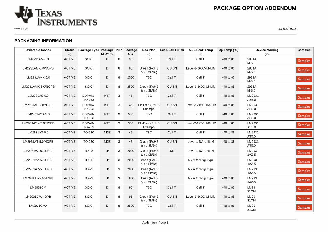
PACKAGING INFORMATION
Orderable Device Status(1)
Package Type PackageDrawing
Pins PackageQty
Eco Plan(2)
Lead/Ball Finish MSL Peak Temp(3)
Op Temp (°C) Device Marking(4/5)
Samples
LM2931AM-5.0 ACTIVE SOIC D 8 95 TBD Call TI Call TI -40 to 85 2931AM-5.0
LM2931AM-5.0/NOPB ACTIVE SOIC D 8 95 Green (RoHS& no Sb/Br)
CU SN Level-1-260C-UNLIM -40 to 85 2931AM-5.0
LM2931AMX-5.0 ACTIVE SOIC D 8 2500 TBD Call TI Call TI -40 to 85 2931AM-5.0
LM2931AMX-5.0/NOPB ACTIVE SOIC D 8 2500 Green (RoHS& no Sb/Br)
CU SN Level-1-260C-UNLIM -40 to 85 2931AM-5.0
LM2931AS-5.0 ACTIVE DDPAK/TO-263
KTT 3 45 TBD Call TI Call TI -40 to 85 LM2931AS5.0
LM2931AS-5.0/NOPB ACTIVE DDPAK/TO-263
KTT 3 45 Pb-Free (RoHSExempt)
CU SN Level-3-245C-168 HR -40 to 85 LM2931AS5.0
LM2931ASX-5.0 ACTIVE DDPAK/TO-263
KTT 3 500 TBD Call TI Call TI -40 to 85 LM2931AS5.0
LM2931ASX-5.0/NOPB ACTIVE DDPAK/TO-263
KTT 3 500 Pb-Free (RoHSExempt)
CU SN Level-3-245C-168 HR -40 to 85 LM2931AS5.0
LM2931AT-5.0 ACTIVE TO-220 NDE 3 45 TBD Call TI Call TI -40 to 85 LM2931AT5.0
LM2931AT-5.0/NOPB ACTIVE TO-220 NDE 3 45 Green (RoHS& no Sb/Br)
CU SN Level-1-NA-UNLIM -40 to 85 LM2931AT5.0
LM2931AZ-5.0/LFT1 ACTIVE TO-92 LP 3 2000 Green (RoHS& no Sb/Br)
SN Level-1-NA-UNLIM LM2931AZ-5
LM2931AZ-5.0/LFT3 ACTIVE TO-92 LP 3 2000 Green (RoHS& no Sb/Br)
N / A for Pkg Type LM2931AZ-5
LM2931AZ-5.0/LFT4 ACTIVE TO-92 LP 3 2000 Green (RoHS& no Sb/Br)
N / A for Pkg Type LM2931AZ-5
LM2931AZ-5.0/NOPB ACTIVE TO-92 LP 3 1800 Green (RoHS& no Sb/Br)
N / A for Pkg Type -40 to 85 LM2931AZ-5
LM2931CM ACTIVE SOIC D 8 95 TBD Call TI Call TI -40 to 85 LM2931CM
LM2931CM/NOPB ACTIVE SOIC D 8 95 Green (RoHS& no Sb/Br)
CU SN Level-1-260C-UNLIM -40 to 85 LM2931CM
LM2931CMX ACTIVE SOIC D 8 2500 TBD Call TI Call TI -40 to 85 LM2931CM
PACKAGE OPTION ADDENDUM
www.ti.com 13-Sep-2013
Addendum-Page 2
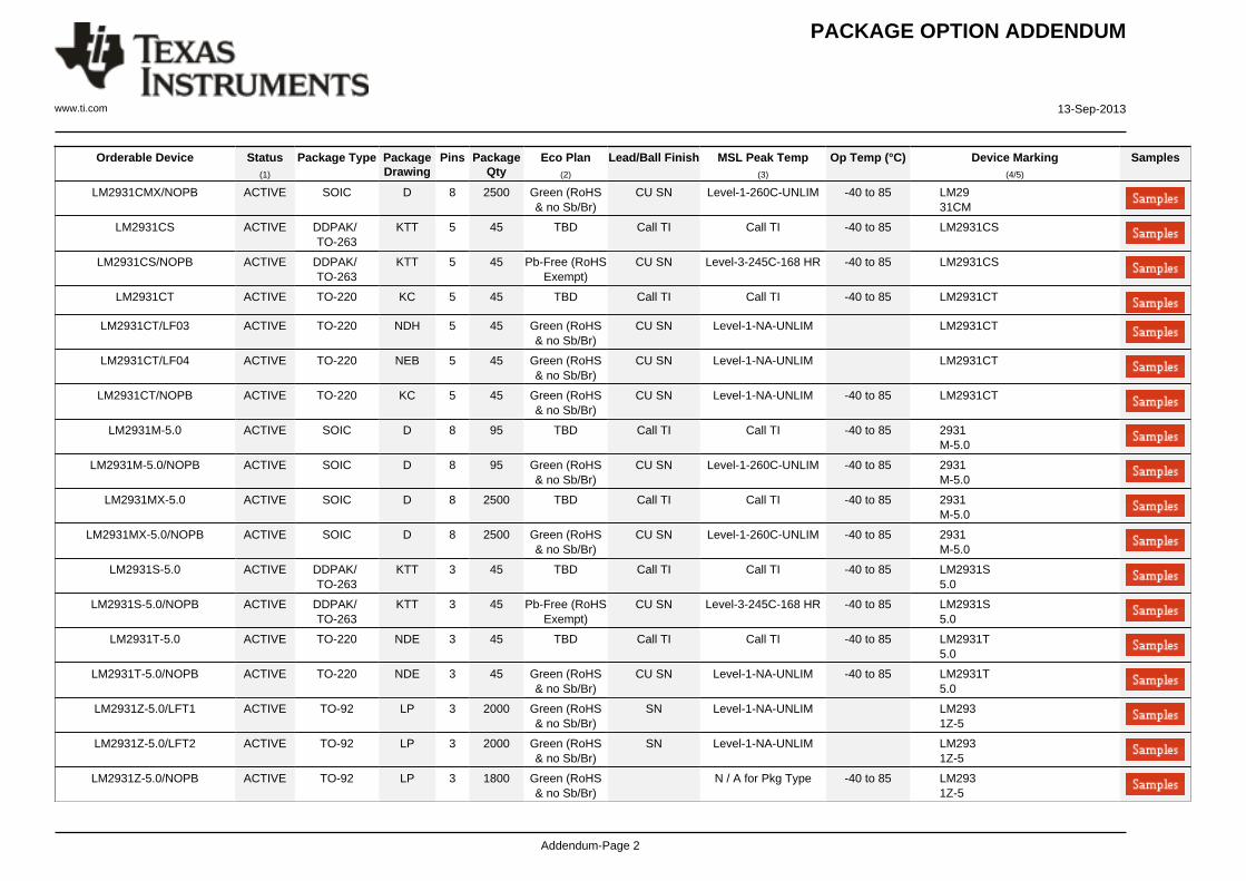
Orderable Device Status(1)
Package Type PackageDrawing
Pins PackageQty
Eco Plan(2)
Lead/Ball Finish MSL Peak Temp(3)
Op Temp (°C) Device Marking(4/5)
Samples
LM2931CMX/NOPB ACTIVE SOIC D 8 2500 Green (RoHS& no Sb/Br)
CU SN Level-1-260C-UNLIM -40 to 85 LM2931CM
LM2931CS ACTIVE DDPAK/TO-263
KTT 5 45 TBD Call TI Call TI -40 to 85 LM2931CS
LM2931CS/NOPB ACTIVE DDPAK/TO-263
KTT 5 45 Pb-Free (RoHSExempt)
CU SN Level-3-245C-168 HR -40 to 85 LM2931CS
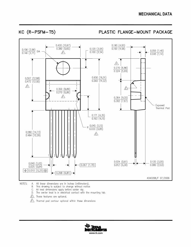
LM2931CT ACTIVE TO-220 KC 5 45 TBD Call TI Call TI -40 to 85 LM2931CT
LM2931CT/LF03 ACTIVE TO-220 NDH 5 45 Green (RoHS& no Sb/Br)
CU SN Level-1-NA-UNLIM LM2931CT
LM2931CT/LF04 ACTIVE TO-220 NEB 5 45 Green (RoHS& no Sb/Br)
CU SN Level-1-NA-UNLIM LM2931CT
LM2931CT/NOPB ACTIVE TO-220 KC 5 45 Green (RoHS& no Sb/Br)
CU SN Level-1-NA-UNLIM -40 to 85 LM2931CT
LM2931M-5.0 ACTIVE SOIC D 8 95 TBD Call TI Call TI -40 to 85 2931M-5.0
LM2931M-5.0/NOPB ACTIVE SOIC D 8 95 Green (RoHS& no Sb/Br)
CU SN Level-1-260C-UNLIM -40 to 85 2931M-5.0
LM2931MX-5.0 ACTIVE SOIC D 8 2500 TBD Call TI Call TI -40 to 85 2931M-5.0
LM2931MX-5.0/NOPB ACTIVE SOIC D 8 2500 Green (RoHS& no Sb/Br)
CU SN Level-1-260C-UNLIM -40 to 85 2931M-5.0
LM2931S-5.0 ACTIVE DDPAK/TO-263
KTT 3 45 TBD Call TI Call TI -40 to 85 LM2931S5.0
LM2931S-5.0/NOPB ACTIVE DDPAK/TO-263
KTT 3 45 Pb-Free (RoHSExempt)
CU SN Level-3-245C-168 HR -40 to 85 LM2931S5.0
LM2931T-5.0 ACTIVE TO-220 NDE 3 45 TBD Call TI Call TI -40 to 85 LM2931T5.0
LM2931T-5.0/NOPB ACTIVE TO-220 NDE 3 45 Green (RoHS& no Sb/Br)
CU SN Level-1-NA-UNLIM -40 to 85 LM2931T5.0
LM2931Z-5.0/LFT1 ACTIVE TO-92 LP 3 2000 Green (RoHS& no Sb/Br)
SN Level-1-NA-UNLIM LM2931Z-5
LM2931Z-5.0/LFT2 ACTIVE TO-92 LP 3 2000 Green (RoHS& no Sb/Br)
SN Level-1-NA-UNLIM LM2931Z-5
LM2931Z-5.0/NOPB ACTIVE TO-92 LP 3 1800 Green (RoHS& no Sb/Br)
N / A for Pkg Type -40 to 85 LM2931Z-5
PACKAGE OPTION ADDENDUM
www.ti.com 13-Sep-2013
Addendum-Page 3
(1) The marketing status values are defined as follows:ACTIVE: Product device recommended for new designs.LIFEBUY: TI has announced that the device will be discontinued, and a lifetime-buy period is in effect.NRND: Not recommended for new designs. Device is in production to support existing customers, but TI does not recommend using this part in a new design.PREVIEW: Device has been announced but is not in production. Samples may or may not be available.OBSOLETE: TI has discontinued the production of the device.
(2) Eco Plan - The planned eco-friendly classification: Pb-Free (RoHS), Pb-Free (RoHS Exempt), or Green (RoHS & no Sb/Br) - please check http://www.ti.com/productcontent for the latest availabilityinformation and additional product content details.TBD: The Pb-Free/Green conversion plan has not been defined.Pb-Free (RoHS): TI's terms "Lead-Free" or "Pb-Free" mean semiconductor products that are compatible with the current RoHS requirements for all 6 substances, including the requirement thatlead not exceed 0.1% by weight in homogeneous materials. Where designed to be soldered at high temperatures, TI Pb-Free products are suitable for use in specified lead-free processes.Pb-Free (RoHS Exempt): This component has a RoHS exemption for either 1) lead-based flip-chip solder bumps used between the die and package, or 2) lead-based die adhesive used betweenthe die and leadframe. The component is otherwise considered Pb-Free (RoHS compatible) as defined above.Green (RoHS & no Sb/Br): TI defines "Green" to mean Pb-Free (RoHS compatible), and free of Bromine (Br) and Antimony (Sb) based flame retardants (Br or Sb do not exceed 0.1% by weightin homogeneous material)
(3) MSL, Peak Temp. -- The Moisture Sensitivity Level rating according to the JEDEC industry standard classifications, and peak solder temperature.
(4) There may be additional marking, which relates to the logo, the lot trace code information, or the environmental category on the device.
(5) Multiple Device Markings will be inside parentheses. Only one Device Marking contained in parentheses and separated by a "~" will appear on a device. If a line is indented then it is a continuationof the previous line and the two combined represent the entire Device Marking for that device.
Important Information and Disclaimer:The information provided on this page represents TI's knowledge and belief as of the date that it is provided. TI bases its knowledge and belief on informationprovided by third parties, and makes no representation or warranty as to the accuracy of such information. Efforts are underway to better integrate information from third parties. TI has taken andcontinues to take reasonable steps to provide representative and accurate information but may not have conducted destructive testing or chemical analysis on incoming materials and chemicals.TI and TI suppliers consider certain information to be proprietary, and thus CAS numbers and other limited information may not be available for release.
In no event shall TI's liability arising out of such information exceed the total purchase price of the TI part(s) at issue in this document sold by TI to Customer on an annual basis.
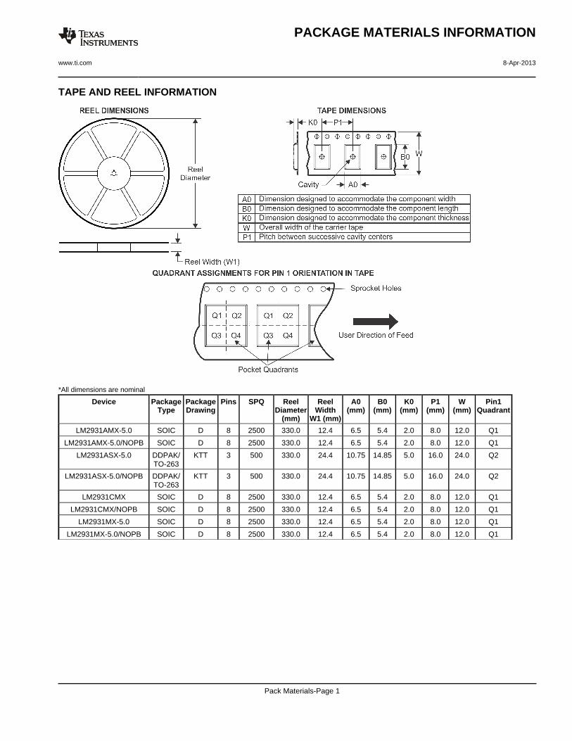
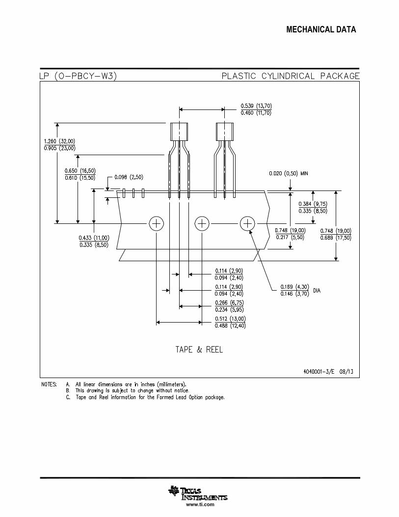
TAPE AND REEL INFORMATION
*All dimensions are nominal
Device PackageType
PackageDrawing
Pins SPQ ReelDiameter
(mm)
ReelWidth
W1 (mm)
A0(mm)
B0(mm)
K0(mm)
P1(mm)
W(mm)
Pin1Quadrant
LM2931AMX-5.0 SOIC D 8 2500 330.0 12.4 6.5 5.4 2.0 8.0 12.0 Q1
LM2931AMX-5.0/NOPB SOIC D 8 2500 330.0 12.4 6.5 5.4 2.0 8.0 12.0 Q1
LM2931ASX-5.0 DDPAK/TO-263
KTT 3 500 330.0 24.4 10.75 14.85 5.0 16.0 24.0 Q2
LM2931ASX-5.0/NOPB DDPAK/TO-263
KTT 3 500 330.0 24.4 10.75 14.85 5.0 16.0 24.0 Q2
LM2931CMX SOIC D 8 2500 330.0 12.4 6.5 5.4 2.0 8.0 12.0 Q1
LM2931CMX/NOPB SOIC D 8 2500 330.0 12.4 6.5 5.4 2.0 8.0 12.0 Q1
LM2931MX-5.0 SOIC D 8 2500 330.0 12.4 6.5 5.4 2.0 8.0 12.0 Q1
LM2931MX-5.0/NOPB SOIC D 8 2500 330.0 12.4 6.5 5.4 2.0 8.0 12.0 Q1
PACKAGE MATERIALS INFORMATION
www.ti.com 8-Apr-2013
Pack Materials-Page 1
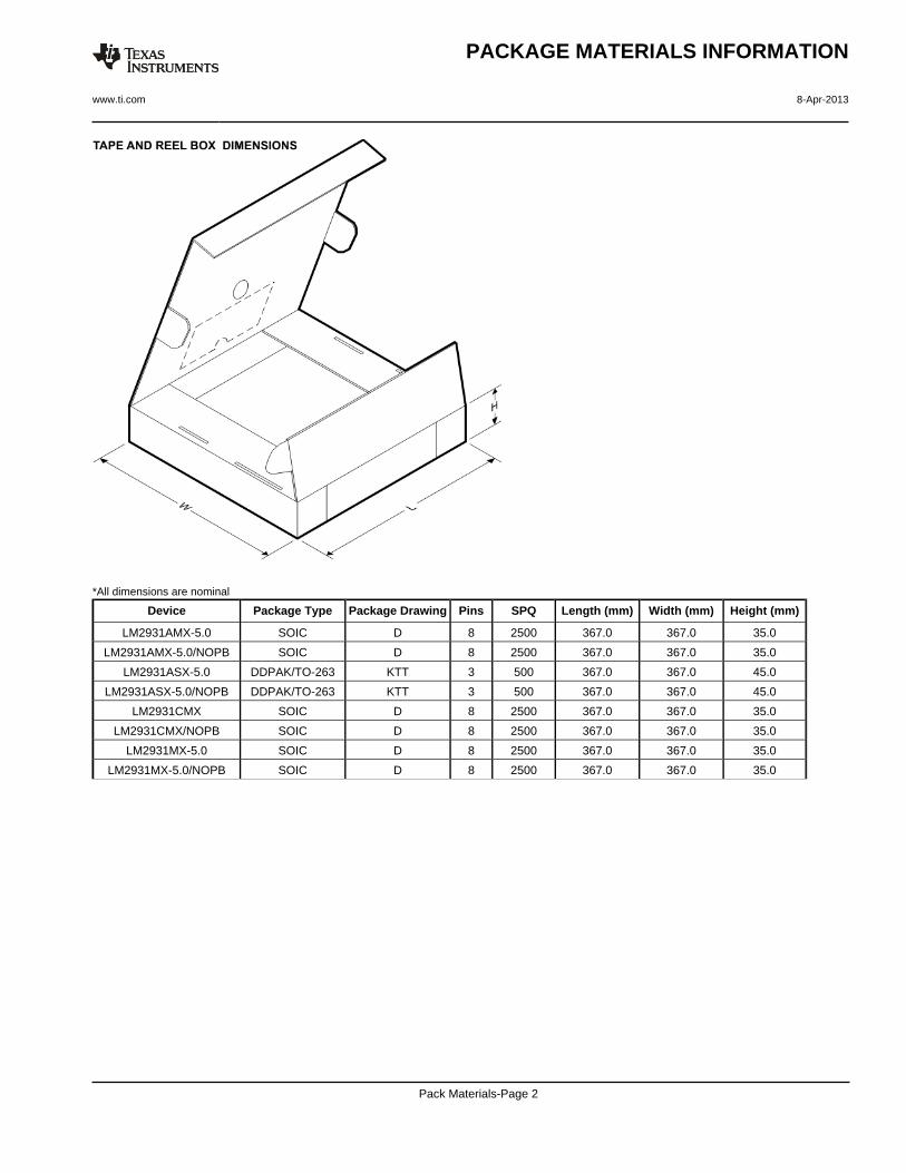
*All dimensions are nominal
Device Package Type Package Drawing Pins SPQ Length (mm) Width (mm) Height (mm)
LM2931AMX-5.0 SOIC D 8 2500 367.0 367.0 35.0
LM2931AMX-5.0/NOPB SOIC D 8 2500 367.0 367.0 35.0
LM2931ASX-5.0 DDPAK/TO-263 KTT 3 500 367.0 367.0 45.0
LM2931ASX-5.0/NOPB DDPAK/TO-263 KTT 3 500 367.0 367.0 45.0
LM2931CMX SOIC D 8 2500 367.0 367.0 35.0
LM2931CMX/NOPB SOIC D 8 2500 367.0 367.0 35.0
LM2931MX-5.0 SOIC D 8 2500 367.0 367.0 35.0
LM2931MX-5.0/NOPB SOIC D 8 2500 367.0 367.0 35.0
PACKAGE MATERIALS INFORMATION
www.ti.com 8-Apr-2013
Pack Materials-Page 2
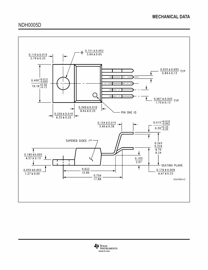
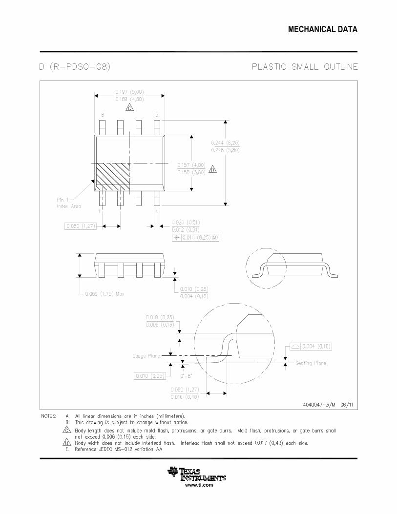
MECHANICAL DATA
NDH0005D
www.ti.com
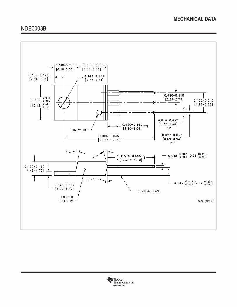
MECHANICAL DATA
NDE0003B
www.ti.com
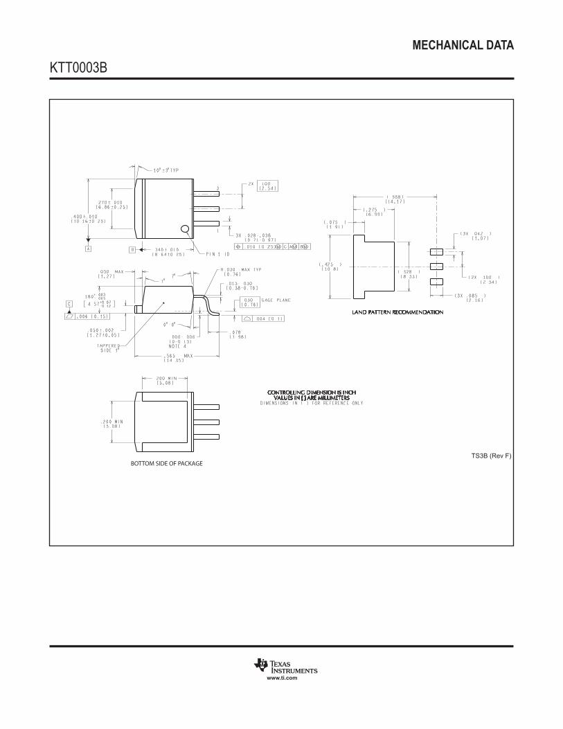
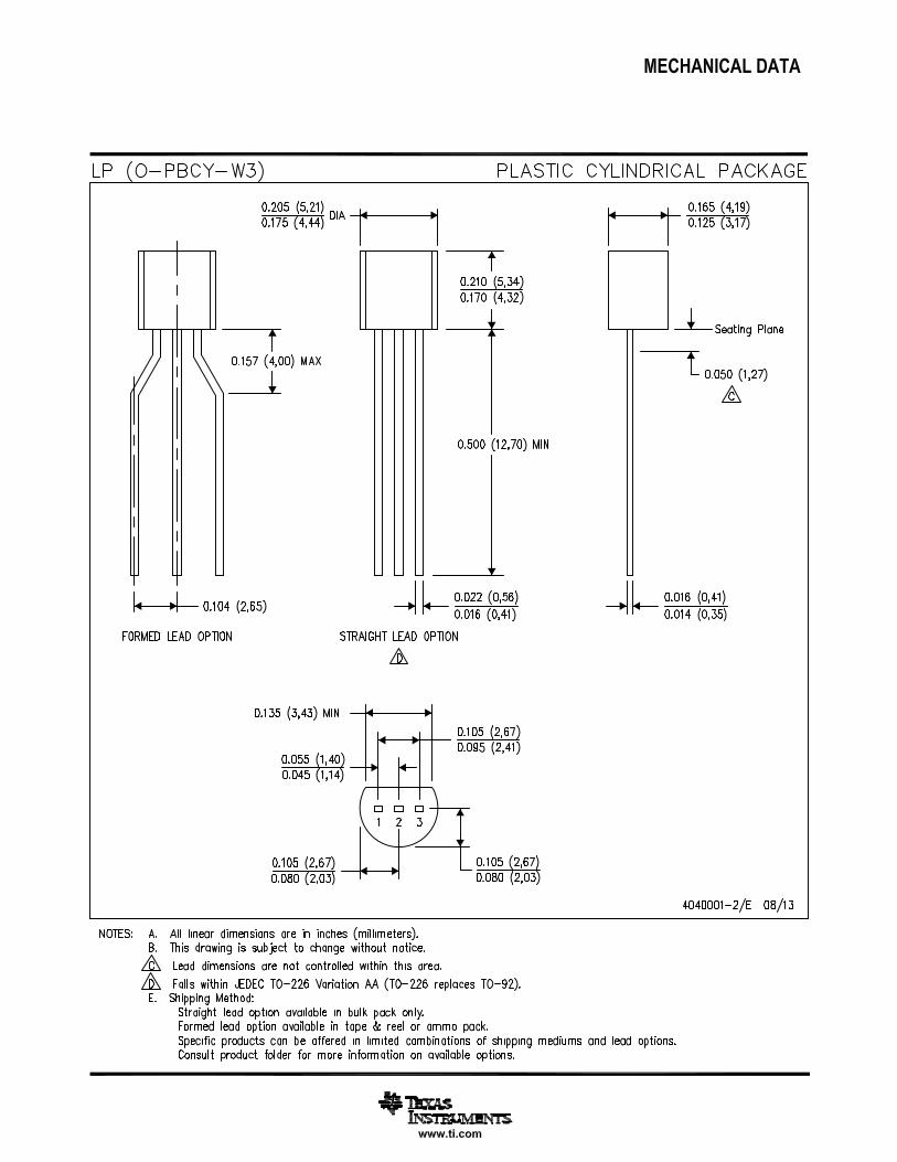
MECHANICAL DATA
KTT0003B
www.ti.com
BOTTOM SIDE OF PACKAGETS3B (Rev F)
MECHANICAL DATA
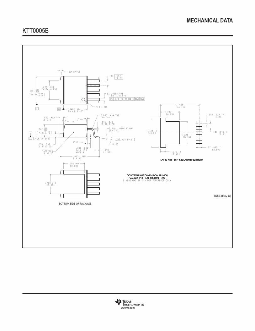
KTT0005B
www.ti.com
BOTTOM SIDE OF PACKAGE
TS5B (Rev D)
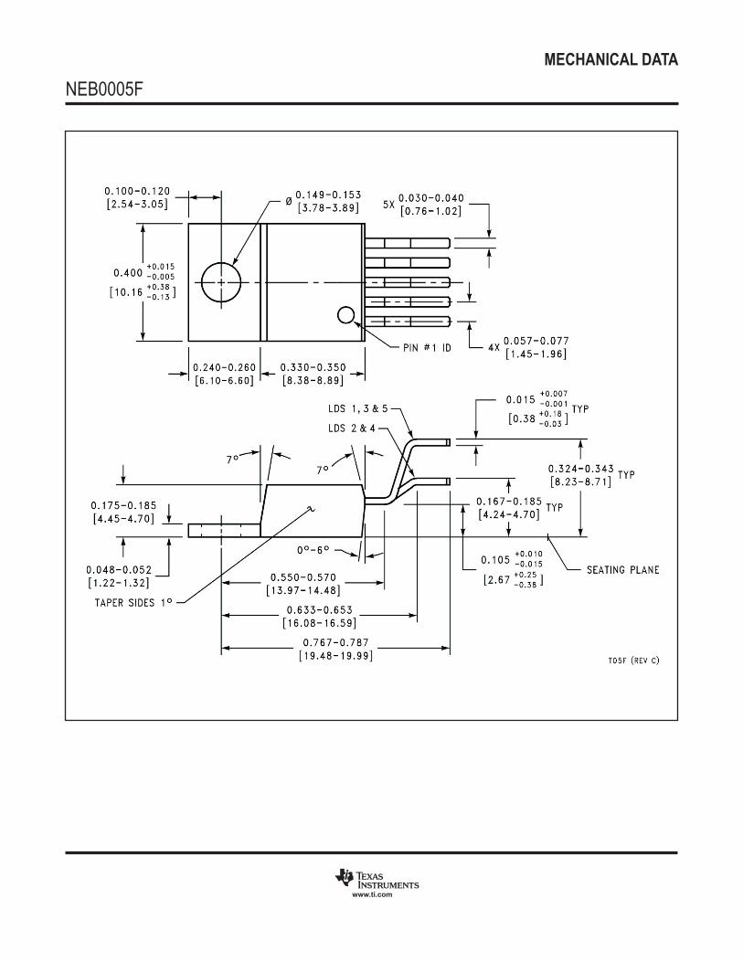
MECHANICAL DATA
NEB0005F
www.ti.com
IMPORTANT NOTICE
Texas Instruments Incorporated and its subsidiaries (TI) reserve the right to make corrections, enhancements, improvements and otherchanges to its semiconductor products and services per JESD46, latest issue, and to discontinue any product or service per JESD48, latestissue. Buyers should obtain the latest relevant information before placing orders and should verify that such information is current andcomplete. All semiconductor products (also referred to herein as “components”) are sold subject to TI’s terms and conditions of salesupplied at the time of order acknowledgment.
TI warrants performance of its components to the specifications applicable at the time of sale, in accordance with the warranty in TI’s termsand conditions of sale of semiconductor products. Testing and other quality control techniques are used to the extent TI deems necessaryto support this warranty. Except where mandated by applicable law, testing of all parameters of each component is not necessarilyperformed.
TI assumes no liability for applications assistance or the design of Buyers’ products. Buyers are responsible for their products andapplications using TI components. To minimize the risks associated with Buyers’ products and applications, Buyers should provideadequate design and operating safeguards.
TI does not warrant or represent that any license, either express or implied, is granted under any patent right, copyright, mask work right, orother intellectual property right relating to any combination, machine, or process in which TI components or services are used. Informationpublished by TI regarding third-party products or services does not constitute a license to use such products or services or a warranty orendorsement thereof. Use of such information may require a license from a third party under the patents or other intellectual property of thethird party, or a license from TI under the patents or other intellectual property of TI.
Reproduction of significant portions of TI information in TI data books or data sheets is permissible only if reproduction is without alterationand is accompanied by all associated warranties, conditions, limitations, and notices. TI is not responsible or liable for such altereddocumentation. Information of third parties may be subject to additional restrictions.
Resale of TI components or services with statements different from or beyond the parameters stated by TI for that component or servicevoids all express and any implied warranties for the associated TI component or service and is an unfair and deceptive business practice.TI is not responsible or liable for any such statements.
Buyer acknowledges and agrees that it is solely responsible for compliance with all legal, regulatory and safety-related requirementsconcerning its products, and any use of TI components in its applications, notwithstanding any applications-related information or supportthat may be provided by TI. Buyer represents and agrees that it has all the necessary expertise to create and implement safeguards whichanticipate dangerous consequences of failures, monitor failures and their consequences, lessen the likelihood of failures that might causeharm and take appropriate remedial actions. Buyer will fully indemnify TI and its representatives against any damages arising out of the useof any TI components in safety-critical applications.
In some cases, TI components may be promoted specifically to facilitate safety-related applications. With such components, TI’s goal is tohelp enable customers to design and create their own end-product solutions that meet applicable functional safety standards andrequirements. Nonetheless, such components are subject to these terms.
No TI components are authorized for use in FDA Class III (or similar life-critical medical equipment) unless authorized officers of the partieshave executed a special agreement specifically governing such use.
Only those TI components which TI has specifically designated as military grade or “enhanced plastic” are designed and intended for use inmilitary/aerospace applications or environments. Buyer acknowledges and agrees that any military or aerospace use of TI componentswhich have not been so designated is solely at the Buyer's risk, and that Buyer is solely responsible for compliance with all legal andregulatory requirements in connection with such use.
TI has specifically designated certain components as meeting ISO/TS16949 requirements, mainly for automotive use. In any case of use ofnon-designated products, TI will not be responsible for any failure to meet ISO/TS16949.
Products Applications
Audio www.ti.com/audio Automotive and Transportation www.ti.com/automotive
Amplifiers amplifier.ti.com Communications and Telecom www.ti.com/communications
Data Converters dataconverter.ti.com Computers and Peripherals www.ti.com/computers
DLP® Products www.dlp.com Consumer Electronics www.ti.com/consumer-apps
DSP dsp.ti.com Energy and Lighting www.ti.com/energy
Clocks and Timers www.ti.com/clocks Industrial www.ti.com/industrial
Interface interface.ti.com Medical www.ti.com/medical
Logic logic.ti.com Security www.ti.com/security
Power Mgmt power.ti.com Space, Avionics and Defense www.ti.com/space-avionics-defense
Microcontrollers microcontroller.ti.com Video and Imaging www.ti.com/video
RFID www.ti-rfid.com
OMAP Applications Processors www.ti.com/omap TI E2E Community e2e.ti.com
Wireless Connectivity www.ti.com/wirelessconnectivity
Mailing Address: Texas Instruments, Post Office Box 655303, Dallas, Texas 75265Copyright © 2013, Texas Instruments Incorporated