Embed Size (px)
Citation preview
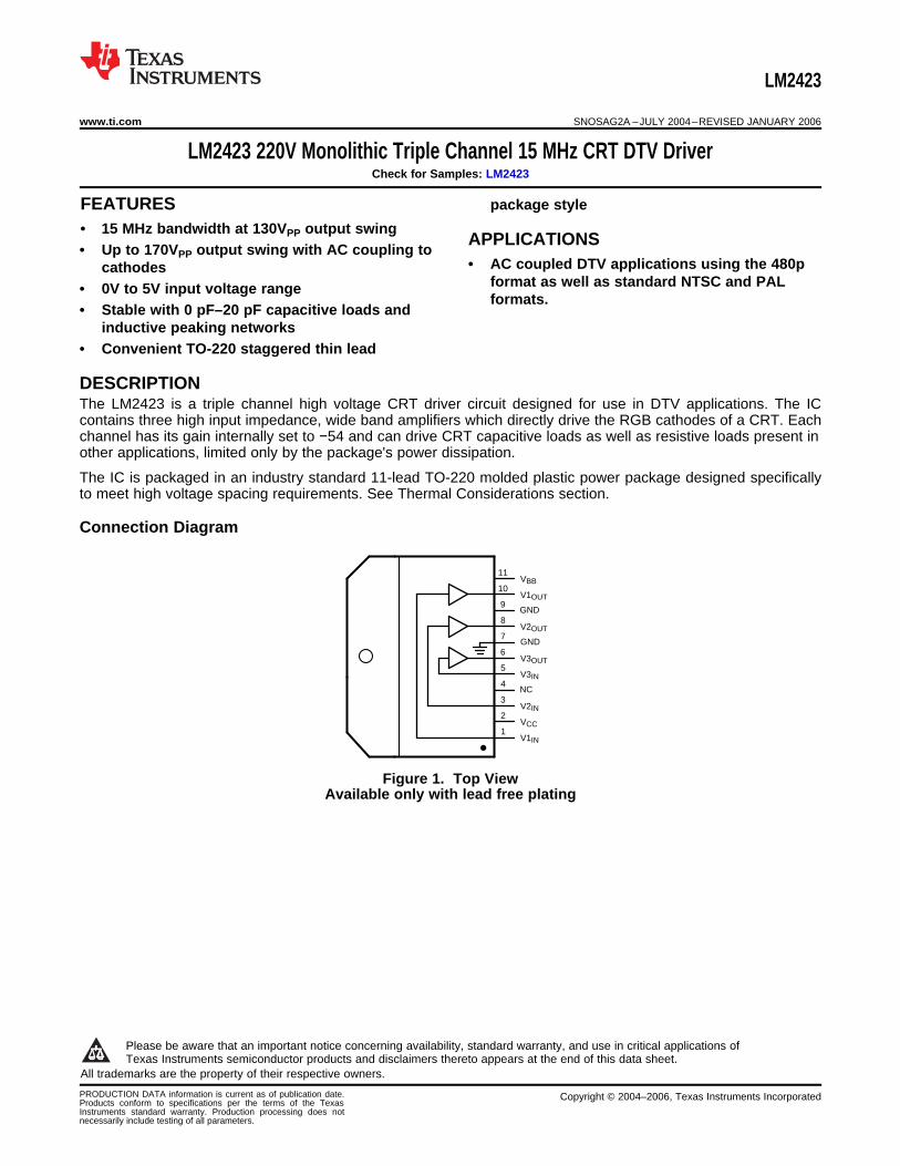
11
10
9
8
7
6
5
4
3
2
1
VBB
V1OUT
GND
V2OUT
GND
V3OUT
V3IN
NC
V2IN
VCC
V1IN
LM2423
www.ti.com SNOSAG2A –JULY 2004–REVISED JANUARY 2006
LM2423 220V Monolithic Triple Channel 15 MHz CRT DTV DriverCheck for Samples: LM2423
1FEATURES package style
2• 15 MHz bandwidth at 130VPP output swingAPPLICATIONS
• Up to 170VPP output swing with AC coupling to• AC coupled DTV applications using the 480pcathodes
format as well as standard NTSC and PAL• 0V to 5V input voltage rangeformats.
• Stable with 0 pF–20 pF capacitive loads andinductive peaking networks
• Convenient TO-220 staggered thin lead
DESCRIPTIONThe LM2423 is a triple channel high voltage CRT driver circuit designed for use in DTV applications. The ICcontains three high input impedance, wide band amplifiers which directly drive the RGB cathodes of a CRT. Eachchannel has its gain internally set to −54 and can drive CRT capacitive loads as well as resistive loads present inother applications, limited only by the package's power dissipation.
The IC is packaged in an industry standard 11-lead TO-220 molded plastic power package designed specificallyto meet high voltage spacing requirements. See Thermal Considerations section.
Connection Diagram
Figure 1. Top ViewAvailable only with lead free plating
1
Please be aware that an important notice concerning availability, standard warranty, and use in critical applications ofTexas Instruments semiconductor products and disclaimers thereto appears at the end of this data sheet.
2All trademarks are the property of their respective owners.
PRODUCTION DATA information is current as of publication date. Copyright © 2004–2006, Texas Instruments IncorporatedProducts conform to specifications per the terms of the TexasInstruments standard warranty. Production processing does notnecessarily include testing of all parameters.
LM2423
SNOSAG2A –JULY 2004–REVISED JANUARY 2006 www.ti.com
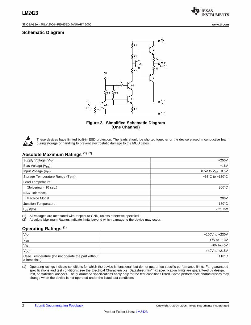
Schematic Diagram
Figure 2. Simplified Schematic Diagram(One Channel)
These devices have limited built-in ESD protection. The leads should be shorted together or the device placed in conductive foamduring storage or handling to prevent electrostatic damage to the MOS gates.
Absolute Maximum Ratings (1) (2)
Supply Voltage (VCC) +250V
Bias Voltage (VBB) +16V
Input Voltage (VIN) −0.5V to VBB +0.5V
Storage Temperature Range (TSTG) −65°C to +150°C
Lead Temperature
(Soldering, <10 sec.) 300°C
ESD Tolerance,
Machine Model 200V
Junction Temperature 150°C
θJC (typ) 2.2°C/W
(1) All voltages are measured with respect to GND, unless otherwise specified.(2) Absolute Maximum Ratings indicate limits beyond which damage to the device may occur.
Operating Ratings (1)
VCC +100V to +230V
VBB +7V to +13V
VIN +0V to +5V
VOUT +40V to +215V
Case Temperature (Do not operate the part without 110°Ca heat sink.)
(1) Operating ratings indicate conditions for which the device is functional, but do not guarantee specific performance limits. For guaranteedspecifications and test conditions, see the Electrical Characteristics. Datasheet min/max specification limits are guaranteed by design,test, or statistical analysis. The guaranteed specifications apply only for the test conditions listed. Some performance characteristics maychange when the device is not operated under the listed test conditions.
2 Submit Documentation Feedback Copyright © 2004–2006, Texas Instruments Incorporated
Product Folder Links: LM2423
+220V+12V
2
CL = 10 pF50:
Output to50: Scope
10 PF 0.1 PF+
11
1,3,5 242310,8,6
+
47 PF 0.1 PF
VADJ
50: 1000:
0.47 PF
0.01 PF
VIN 7 50:
Test Point4990: 4990: 0.1 PF
CompensationCapacitor
from SignalInput
Generator
LM2423
www.ti.com SNOSAG2A –JULY 2004–REVISED JANUARY 2006
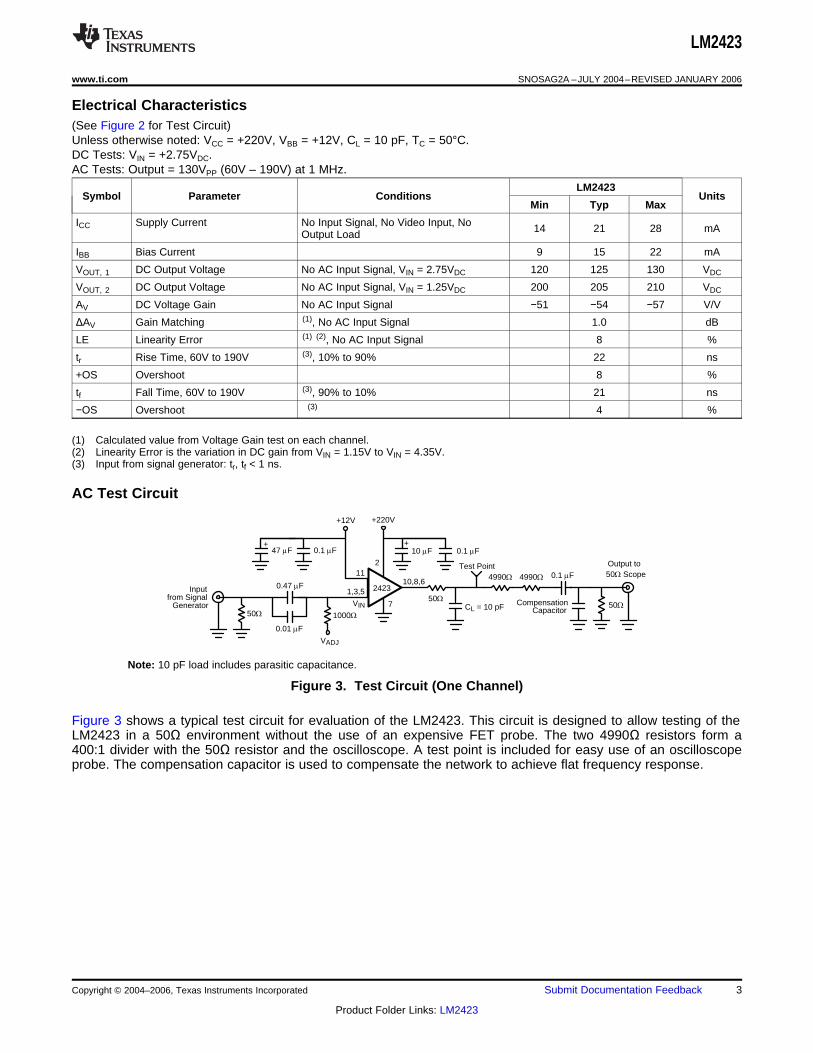
Electrical Characteristics(See Figure 2 for Test Circuit)Unless otherwise noted: VCC = +220V, VBB = +12V, CL = 10 pF, TC = 50°C.DC Tests: VIN = +2.75VDC.AC Tests: Output = 130VPP (60V – 190V) at 1 MHz.
LM2423Symbol Parameter Conditions Units
Min Typ Max
ICC Supply Current No Input Signal, No Video Input, No 14 21 28 mAOutput Load
IBB Bias Current 9 15 22 mA
VOUT, 1 DC Output Voltage No AC Input Signal, VIN = 2.75VDC 120 125 130 VDC
VOUT, 2 DC Output Voltage No AC Input Signal, VIN = 1.25VDC 200 205 210 VDC
AV DC Voltage Gain No AC Input Signal −51 −54 −57 V/V
ΔAV Gain Matching (1), No AC Input Signal 1.0 dB
LE Linearity Error (1) (2), No AC Input Signal 8 %
tr Rise Time, 60V to 190V (3), 10% to 90% 22 ns
+OS Overshoot 8 %
tf Fall Time, 60V to 190V (3), 90% to 10% 21 ns
−OS Overshoot (3) 4 %
(1) Calculated value from Voltage Gain test on each channel.(2) Linearity Error is the variation in DC gain from VIN = 1.15V to VIN = 4.35V.(3) Input from signal generator: tr, tf < 1 ns.
AC Test Circuit
Note: 10 pF load includes parasitic capacitance.
Figure 3. Test Circuit (One Channel)
Figure 3 shows a typical test circuit for evaluation of the LM2423. This circuit is designed to allow testing of theLM2423 in a 50Ω environment without the use of an expensive FET probe. The two 4990Ω resistors form a400:1 divider with the 50Ω resistor and the oscilloscope. A test point is included for easy use of an oscilloscopeprobe. The compensation capacitor is used to compensate the network to achieve flat frequency response.
Copyright © 2004–2006, Texas Instruments Incorporated Submit Documentation Feedback 3
Product Folder Links: LM2423
120 122 124 126 128 130
OFFSET VOLTAGE (V)
20
20.5
21
21.5
22
22.5
23
SP
EE
D (
ns)
tf
tr
30 40 50 60 70 80 90 100 110
CASE TEMPERATURE (°C)
20
20.5
21
21.5
22
22.5
23
23.5
24
SP
EE
D (
ns)
tr
tf
1 10 100
FREQUENCY (MHz)
-18
-15
-12
-9
-6
-3
0
3
MA
GN
ITU
DE
(dB
)
10 12 14 16 18 20
LOAD CAPACITANCE (pF)
20
22
24
26
28
30
SP
EE
D (
ns) tr
tf
0 1 2 3 4 5 6
VIN (V)
0
20
40
60
80
100
120
140
160
180
200
220
VO
UT (
V)
100 ns/DIV
20V
/DIV
tf = 21 nstr = 22 ns
LM2423
SNOSAG2A –JULY 2004–REVISED JANUARY 2006 www.ti.com
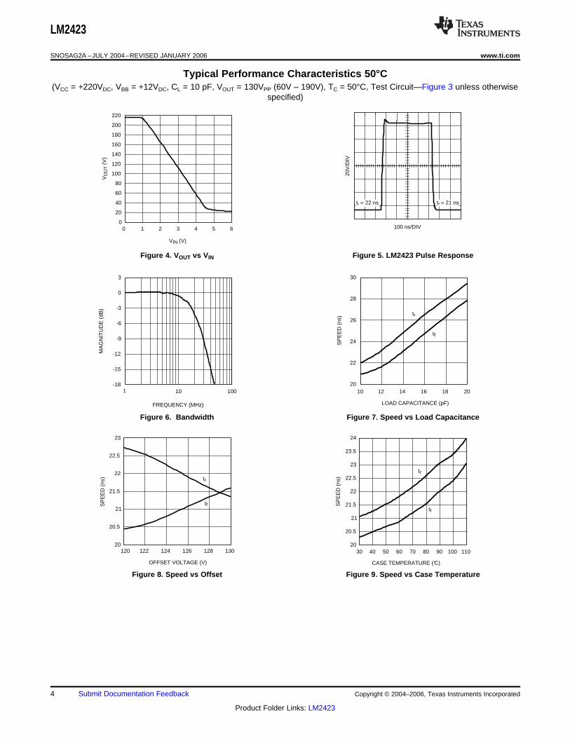
Typical Performance Characteristics 50°C(VCC = +220VDC, VBB = +12VDC, CL = 10 pF, VOUT = 130VPP (60V – 190V), TC = 50°C, Test Circuit—Figure 3 unless otherwise
specified)
Figure 4. VOUT vs VIN Figure 5. LM2423 Pulse Response
Figure 6. Bandwidth Figure 7. Speed vs Load Capacitance
Figure 8. Speed vs Offset Figure 9. Speed vs Case Temperature
4 Submit Documentation Feedback Copyright © 2004–2006, Texas Instruments Incorporated
Product Folder Links: LM2423
100 ns/DIV
20V
/DIV
tr = 25 nstf = 21 ns
0 5 10 15 20 25 30
FREQUENCY (MHz)
6
8
10
12
14
16
18
PO
WE
R D
ISS
IPA
TIO
N (
W)
72% ACTIVE TIME
0 20 40 60 80 100 120 140
CASE TEMPERATURE (°C)
0
3
6
9
12
15
18
PO
WE
R D
ISS
IPA
TIO
N (
W)
LM2423
www.ti.com SNOSAG2A –JULY 2004–REVISED JANUARY 2006
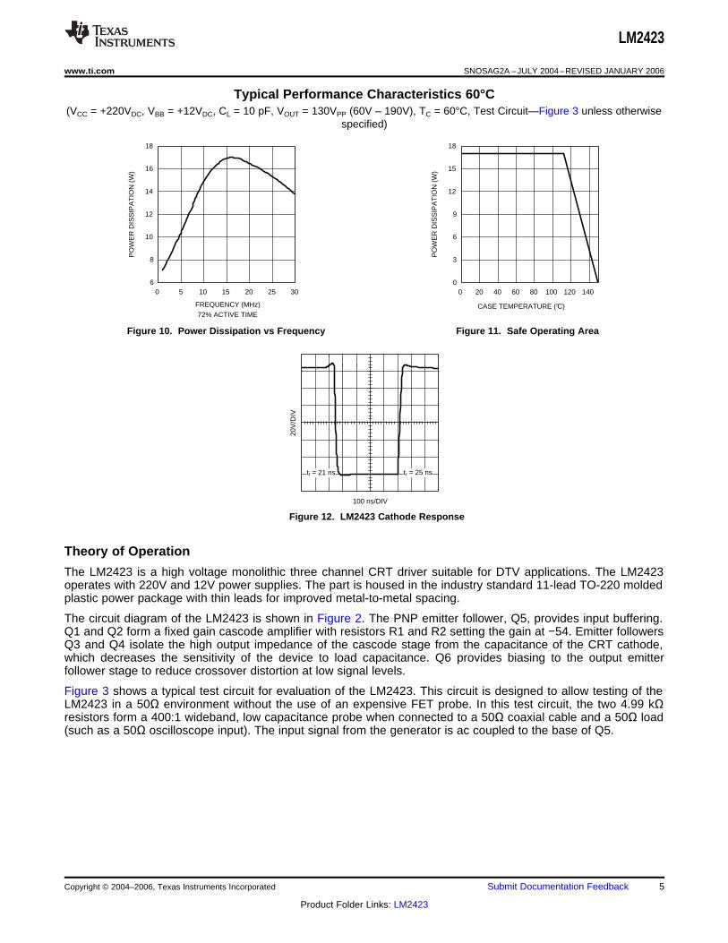
Typical Performance Characteristics 60°C(VCC = +220VDC, VBB = +12VDC, CL = 10 pF, VOUT = 130VPP (60V – 190V), TC = 60°C, Test Circuit—Figure 3 unless otherwise
specified)
Figure 10. Power Dissipation vs Frequency Figure 11. Safe Operating Area
Figure 12. LM2423 Cathode Response
Theory of Operation
The LM2423 is a high voltage monolithic three channel CRT driver suitable for DTV applications. The LM2423operates with 220V and 12V power supplies. The part is housed in the industry standard 11-lead TO-220 moldedplastic power package with thin leads for improved metal-to-metal spacing.
The circuit diagram of the LM2423 is shown in Figure 2. The PNP emitter follower, Q5, provides input buffering.Q1 and Q2 form a fixed gain cascode amplifier with resistors R1 and R2 setting the gain at −54. Emitter followersQ3 and Q4 isolate the high output impedance of the cascode stage from the capacitance of the CRT cathode,which decreases the sensitivity of the device to load capacitance. Q6 provides biasing to the output emitterfollower stage to reduce crossover distortion at low signal levels.
Figure 3 shows a typical test circuit for evaluation of the LM2423. This circuit is designed to allow testing of theLM2423 in a 50Ω environment without the use of an expensive FET probe. In this test circuit, the two 4.99 kΩresistors form a 400:1 wideband, low capacitance probe when connected to a 50Ω coaxial cable and a 50Ω load(such as a 50Ω oscilloscope input). The input signal from the generator is ac coupled to the base of Q5.
Copyright © 2004–2006, Texas Instruments Incorporated Submit Documentation Feedback 5
Product Folder Links: LM2423
2423
+220V+12V
R1
INPUT
R2220:L1 D1
D2 SPARKGAP
CATHODE
C2C1
C3
1/2W1.8 PH360:
LM2423
SNOSAG2A –JULY 2004–REVISED JANUARY 2006 www.ti.com
Application Hints
INTRODUCTION
National Semiconductor (NSC) is committed to provide application information that assists our customers inobtaining the best performance possible from our products. The following information is provided in order tosupport this commitment. The reader should be aware that the optimization of performance was done using aspecific printed circuit board designed at NSC. Variations in performance can be realized due to physicalchanges in the printed circuit board and the application. Therefore, the designer should know that componentvalue changes may be required in order to optimize performance in a given application. The values shown in thisdocument can be used as a starting point for evaluation purposes. When working with high bandwidth circuits,good layout practices are also critical to achieving maximum performance.
IMPORTANT INFORMATION
The LM2423 performance is targeted for the HDTV market. The application circuits shown in this document tooptimize performance and to protect against damage from CRT arc over are designed specifically for theLM2423. If another member of the LM242X family is used, please refer to its datasheet.
POWER SUPPLY BYPASS
Since the LM2423 is a wide bandwidth amplifier, proper power supply bypassing is critical for optimumperformance. Improper power supply bypassing can result in large overshoot, ringing or oscillation. 0.1 µFcapacitors should be connected from the supply pins, VCC and VBB, to ground, as close to the LM2423 as ispractical. Additionally, a 22 µF or larger electrolytic capacitor should be connected from both supply pins toground reasonably close to the LM2423.
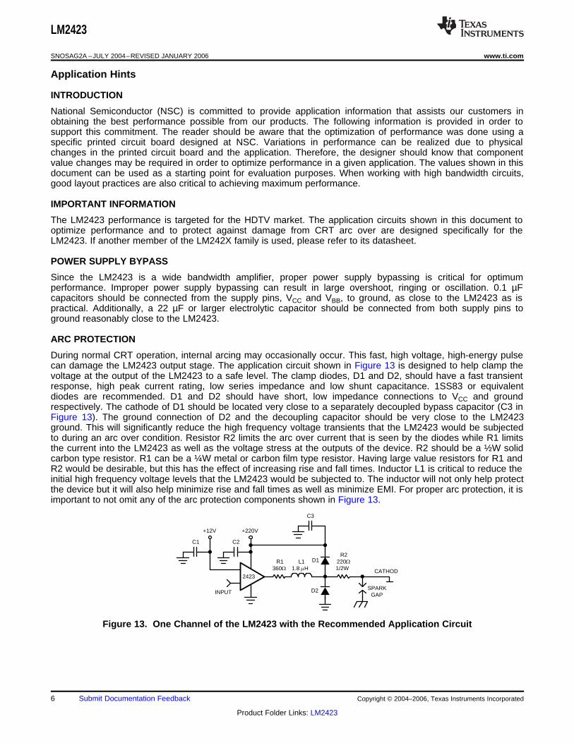
ARC PROTECTION
During normal CRT operation, internal arcing may occasionally occur. This fast, high voltage, high-energy pulsecan damage the LM2423 output stage. The application circuit shown in Figure 13 is designed to help clamp thevoltage at the output of the LM2423 to a safe level. The clamp diodes, D1 and D2, should have a fast transientresponse, high peak current rating, low series impedance and low shunt capacitance. 1SS83 or equivalentdiodes are recommended. D1 and D2 should have short, low impedance connections to VCC and groundrespectively. The cathode of D1 should be located very close to a separately decoupled bypass capacitor (C3 inFigure 13). The ground connection of D2 and the decoupling capacitor should be very close to the LM2423ground. This will significantly reduce the high frequency voltage transients that the LM2423 would be subjectedto during an arc over condition. Resistor R2 limits the arc over current that is seen by the diodes while R1 limitsthe current into the LM2423 as well as the voltage stress at the outputs of the device. R2 should be a ½W solidcarbon type resistor. R1 can be a ¼W metal or carbon film type resistor. Having large value resistors for R1 andR2 would be desirable, but this has the effect of increasing rise and fall times. Inductor L1 is critical to reduce theinitial high frequency voltage levels that the LM2423 would be subjected to. The inductor will not only help protectthe device but it will also help minimize rise and fall times as well as minimize EMI. For proper arc protection, it isimportant to not omit any of the arc protection components shown in Figure 13.
Figure 13. One Channel of the LM2423 with the Recommended Application Circuit
6 Submit Documentation Feedback Copyright © 2004–2006, Texas Instruments Incorporated
Product Folder Links: LM2423
RTH110oC - 60oC
16.9= 3.0oC/W
LM2423
www.ti.com SNOSAG2A –JULY 2004–REVISED JANUARY 2006
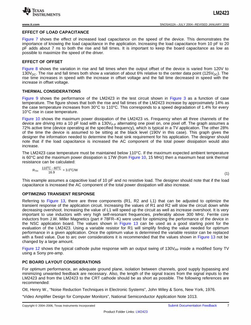
EFFECT OF LOAD CAPACITANCE
Figure 7 shows the effect of increased load capacitance on the speed of the device. This demonstrates theimportance of knowing the load capacitance in the application. Increasing the load capacitance from 10 pF to 20pF adds about 7 ns to both the rise and fall times. It is important to keep the board capacitance as low aspossible to maximize the speed of the driver.
EFFECT OF OFFSET
Figure 8 shows the variation in rise and fall times when the output offset of the device is varied from 120V to130VDC. The rise and fall times both show a variation of about 6% relative to the center data point (125VDC). Therise time increases in speed with the increase in offset voltage and the fall time decreased in speed with theincrease in offset voltage.
THERMAL CONSIDERATIONS
Figure 9 shows the performance of the LM2423 in the test circuit shown in Figure 3 as a function of casetemperature. The figure shows that both the rise and fall times of the LM2423 increase by approximately 14% asthe case temperature increases from 30°C to 110°C. This corresponds to a speed degradation of 1.4% for every10°C rise in case temperature.
Figure 10 shows the maximum power dissipation of the LM2423 vs. Frequency when all three channels of thedevice are driving into a 10 pF load with a 130VP-P alternating one pixel on, one pixel off. The graph assumes a72% active time (device operating at the specified frequency), which is typical in a TV application. The other 28%of the time the device is assumed to be sitting at the black level (190V in this case). This graph gives thedesigner the information needed to determine the heat sink requirement for his application. The designer shouldnote that if the load capacitance is increased the AC component of the total power dissipation would alsoincrease.
The LM2423 case temperature must be maintained below 110°C. If the maximum expected ambient temperatureis 60°C and the maximum power dissipation is 17W (from Figure 10, 15 MHz) then a maximum heat sink thermalresistance can be calculated:
(1)
This example assumes a capacitive load of 10 pF and no resistive load. The designer should note that if the loadcapacitance is increased the AC component of the total power dissipation will also increase.
OPTIMIZING TRANSIENT RESPONSE
Referring to Figure 13, there are three components (R1, R2 and L1) that can be adjusted to optimize thetransient response of the application circuit. Increasing the values of R1 and R2 will slow the circuit down whiledecreasing overshoot. Increasing the value of L1 will speed up the circuit as well as increase overshoot. It is veryimportant to use inductors with very high self-resonant frequencies, preferably above 300 MHz. Ferrite coreinductors from J.W. Miller Magnetics (part # 78FR--K) were used for optimizing the performance of the device inthe NSC application board. The values shown in Figure 13 can be used as a good starting point for theevaluation of the LM2423. Using a variable resistor for R1 will simplify finding the value needed for optimumperformance in a given application. Once the optimum value is determined the variable resistor can be replacedwith a fixed value. Due to arc over considerations it is recommended that the values shown in Figure 13 not bechanged by a large amount.
Figure 12 shows the typical cathode pulse response with an output swing of 130VPP inside a modified Sony TVusing a Sony pre-amp.
PC BOARD LAYOUT CONSIDERATIONS
For optimum performance, an adequate ground plane, isolation between channels, good supply bypassing andminimizing unwanted feedback are necessary. Also, the length of the signal traces from the signal inputs to theLM2423 and from the LM2423 to the CRT cathode should be as short as possible. The following references arerecommended:
Ott, Henry W., “Noise Reduction Techniques in Electronic Systems”, John Wiley & Sons, New York, 1976.
“Video Amplifier Design for Computer Monitors”, National Semiconductor Application Note 1013.
Copyright © 2004–2006, Texas Instruments Incorporated Submit Documentation Feedback 7
Product Folder Links: LM2423
LM2423
SNOSAG2A –JULY 2004–REVISED JANUARY 2006 www.ti.com
Pease, Robert A., “Troubleshooting Analog Circuits”, Butterworth-Heinemann, 1991.
Because of its high small signal bandwidth, the part may oscillate in a TV if feedback occurs around the videochannel through the chassis wiring. To prevent this, leads to the video amplifier input circuit should be shielded,and input circuit wiring should be spaced as far as possible from output circuit wiring.
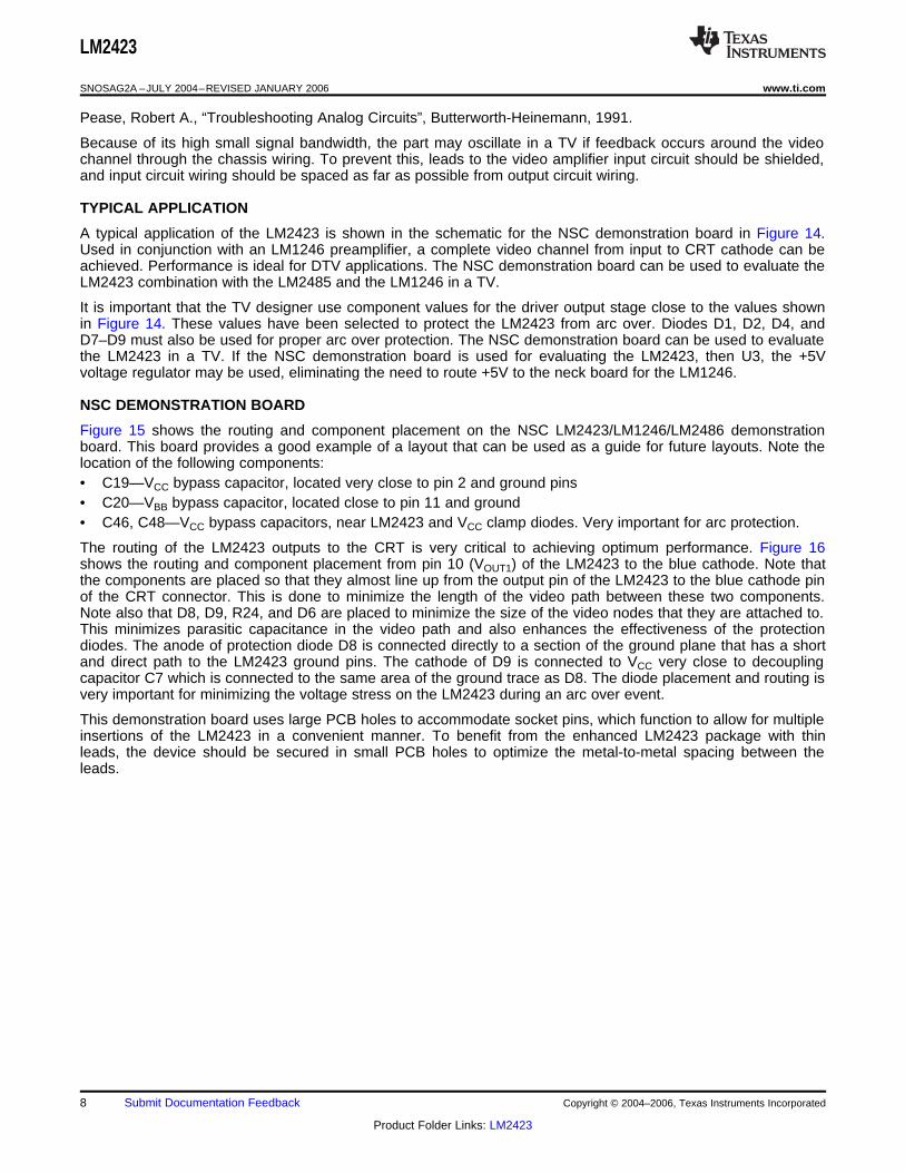
TYPICAL APPLICATION
A typical application of the LM2423 is shown in the schematic for the NSC demonstration board in Figure 14.Used in conjunction with an LM1246 preamplifier, a complete video channel from input to CRT cathode can beachieved. Performance is ideal for DTV applications. The NSC demonstration board can be used to evaluate theLM2423 combination with the LM2485 and the LM1246 in a TV.
It is important that the TV designer use component values for the driver output stage close to the values shownin Figure 14. These values have been selected to protect the LM2423 from arc over. Diodes D1, D2, D4, andD7–D9 must also be used for proper arc over protection. The NSC demonstration board can be used to evaluatethe LM2423 in a TV. If the NSC demonstration board is used for evaluating the LM2423, then U3, the +5Vvoltage regulator may be used, eliminating the need to route +5V to the neck board for the LM1246.
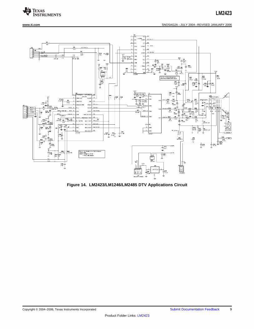
NSC DEMONSTRATION BOARD
Figure 15 shows the routing and component placement on the NSC LM2423/LM1246/LM2486 demonstrationboard. This board provides a good example of a layout that can be used as a guide for future layouts. Note thelocation of the following components:• C19—VCC bypass capacitor, located very close to pin 2 and ground pins• C20—VBB bypass capacitor, located close to pin 11 and ground• C46, C48—VCC bypass capacitors, near LM2423 and VCC clamp diodes. Very important for arc protection.
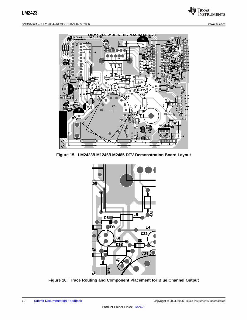
The routing of the LM2423 outputs to the CRT is very critical to achieving optimum performance. Figure 16shows the routing and component placement from pin 10 (VOUT1) of the LM2423 to the blue cathode. Note thatthe components are placed so that they almost line up from the output pin of the LM2423 to the blue cathode pinof the CRT connector. This is done to minimize the length of the video path between these two components.Note also that D8, D9, R24, and D6 are placed to minimize the size of the video nodes that they are attached to.This minimizes parasitic capacitance in the video path and also enhances the effectiveness of the protectiondiodes. The anode of protection diode D8 is connected directly to a section of the ground plane that has a shortand direct path to the LM2423 ground pins. The cathode of D9 is connected to VCC very close to decouplingcapacitor C7 which is connected to the same area of the ground trace as D8. The diode placement and routing isvery important for minimizing the voltage stress on the LM2423 during an arc over event.
This demonstration board uses large PCB holes to accommodate socket pins, which function to allow for multipleinsertions of the LM2423 in a convenient manner. To benefit from the enhanced LM2423 package with thinleads, the device should be secured in small PCB holes to optimize the metal-to-metal spacing between theleads.
8 Submit Documentation Feedback Copyright © 2004–2006, Texas Instruments Incorporated
Product Folder Links: LM2423
LM2423
www.ti.com SNOSAG2A –JULY 2004–REVISED JANUARY 2006
Figure 14. LM2423/LM1246/LM2485 DTV Applications Circuit
Copyright © 2004–2006, Texas Instruments Incorporated Submit Documentation Feedback 9
Product Folder Links: LM2423
LM2423
SNOSAG2A –JULY 2004–REVISED JANUARY 2006 www.ti.com
Figure 15. LM2423/LM1246/LM2485 DTV Demonstration Board Layout
Figure 16. Trace Routing and Component Placement for Blue Channel Output
10 Submit Documentation Feedback Copyright © 2004–2006, Texas Instruments Incorporated
Product Folder Links: LM2423

IMPORTANT NOTICE
Texas Instruments Incorporated and its subsidiaries (TI) reserve the right to make corrections, enhancements, improvements and otherchanges to its semiconductor products and services per JESD46, latest issue, and to discontinue any product or service per JESD48, latestissue. Buyers should obtain the latest relevant information before placing orders and should verify that such information is current andcomplete. All semiconductor products (also referred to herein as “components”) are sold subject to TI’s terms and conditions of salesupplied at the time of order acknowledgment.
TI warrants performance of its components to the specifications applicable at the time of sale, in accordance with the warranty in TI’s termsand conditions of sale of semiconductor products. Testing and other quality control techniques are used to the extent TI deems necessaryto support this warranty. Except where mandated by applicable law, testing of all parameters of each component is not necessarilyperformed.
TI assumes no liability for applications assistance or the design of Buyers’ products. Buyers are responsible for their products andapplications using TI components. To minimize the risks associated with Buyers’ products and applications, Buyers should provideadequate design and operating safeguards.
TI does not warrant or represent that any license, either express or implied, is granted under any patent right, copyright, mask work right, orother intellectual property right relating to any combination, machine, or process in which TI components or services are used. Informationpublished by TI regarding third-party products or services does not constitute a license to use such products or services or a warranty orendorsement thereof. Use of such information may require a license from a third party under the patents or other intellectual property of thethird party, or a license from TI under the patents or other intellectual property of TI.
Reproduction of significant portions of TI information in TI data books or data sheets is permissible only if reproduction is without alterationand is accompanied by all associated warranties, conditions, limitations, and notices. TI is not responsible or liable for such altereddocumentation. Information of third parties may be subject to additional restrictions.
Resale of TI components or services with statements different from or beyond the parameters stated by TI for that component or servicevoids all express and any implied warranties for the associated TI component or service and is an unfair and deceptive business practice.TI is not responsible or liable for any such statements.
Buyer acknowledges and agrees that it is solely responsible for compliance with all legal, regulatory and safety-related requirementsconcerning its products, and any use of TI components in its applications, notwithstanding any applications-related information or supportthat may be provided by TI. Buyer represents and agrees that it has all the necessary expertise to create and implement safeguards whichanticipate dangerous consequences of failures, monitor failures and their consequences, lessen the likelihood of failures that might causeharm and take appropriate remedial actions. Buyer will fully indemnify TI and its representatives against any damages arising out of the useof any TI components in safety-critical applications.
In some cases, TI components may be promoted specifically to facilitate safety-related applications. With such components, TI’s goal is tohelp enable customers to design and create their own end-product solutions that meet applicable functional safety standards andrequirements. Nonetheless, such components are subject to these terms.
No TI components are authorized for use in FDA Class III (or similar life-critical medical equipment) unless authorized officers of the partieshave executed a special agreement specifically governing such use.
Only those TI components which TI has specifically designated as military grade or “enhanced plastic” are designed and intended for use inmilitary/aerospace applications or environments. Buyer acknowledges and agrees that any military or aerospace use of TI componentswhich have not been so designated is solely at the Buyer's risk, and that Buyer is solely responsible for compliance with all legal andregulatory requirements in connection with such use.
TI has specifically designated certain components which meet ISO/TS16949 requirements, mainly for automotive use. Components whichhave not been so designated are neither designed nor intended for automotive use; and TI will not be responsible for any failure of suchcomponents to meet such requirements.
Products Applications
Audio www.ti.com/audio Automotive and Transportation www.ti.com/automotive
Amplifiers amplifier.ti.com Communications and Telecom www.ti.com/communications
Data Converters dataconverter.ti.com Computers and Peripherals www.ti.com/computers
DLP® Products www.dlp.com Consumer Electronics www.ti.com/consumer-apps
DSP dsp.ti.com Energy and Lighting www.ti.com/energy
Clocks and Timers www.ti.com/clocks Industrial www.ti.com/industrial
Interface interface.ti.com Medical www.ti.com/medical
Logic logic.ti.com Security www.ti.com/security
Power Mgmt power.ti.com Space, Avionics and Defense www.ti.com/space-avionics-defense
Microcontrollers microcontroller.ti.com Video and Imaging www.ti.com/video
RFID www.ti-rfid.com
OMAP Applications Processors www.ti.com/omap TI E2E Community e2e.ti.com
Wireless Connectivity www.ti.com/wirelessconnectivity
Mailing Address: Texas Instruments, Post Office Box 655303, Dallas, Texas 75265Copyright © 2012, Texas Instruments Incorporated

Mouser Electronics
Authorized Distributor
Click to View Pricing, Inventory, Delivery & Lifecycle Information: Texas Instruments:
LM2423TE/NOPB
![3)]8][]1 y]/]d]' Eyukio-sekiguchi.way-nifty.com/radio/files/jst135_lpf1.pdf · 20 dB Attenuator, Out 10 dB Attenuator, Out Preamp, Out PTT, Out GND NC NC NC GND NC NC NC D107_ D106_](https://img.pdfslide.us/doc/110x75/60970f0eb14ddc765540dfeb/381-yd-eyukio-20-db-attenuator-out-10-db-attenuator-out-preamp-out.jpg)


![Wireless Starter Kit Mainboard - Silicon Labs · vcom_enable pti0[0..2] vmcu gnd gnd gnd gnd vmcu vrf 5v 3v3 gnd vrf gnd gnd gnd gnd gnd usb_vbus usb_vreg usb_vbus 5v 5v_dbg …](https://img.pdfslide.us/doc/110x75/5ac0fbea7f8b9a4e7c8c7c14/wireless-starter-kit-mainboard-silicon-labs-pti002-vmcu-gnd-gnd-gnd-gnd-vmcu.jpg)