Embed Size (px)
Citation preview

LM148/LM248/LM348Quad 741 Op AmpsLM149Wide Band Decompensated (A V (MIN) = 5)General DescriptionThe LM148 series is a true quad 741. It consists of fourindependent, high gain, internally compensated, low poweroperational amplifiers which have been designed to providefunctional characteristics identical to those of the familiar741 operational amplifier. In addition the total supply currentfor all four amplifiers is comparable to the supply current of asingle 741 type op amp. Other features include input offsetcurrents and input bias current which are much less thanthose of a standard 741. Also, excellent isolation betweenamplifiers has been achieved by independently biasing eachamplifier and using layout techniques which minimizethermal coupling. The LM149 series has the same featuresas the LM148 plus a gain bandwidth product of 4 MHz at again of 5 or greater.
The LM148 can be used anywhere multiple 741 or 1558 typeamplifiers are being used and in applications where amplifiermatching or high packing density is required. For lowerpower refer to LF444.
Featuresn 741 op amp operating characteristicsn Class AB output stage — no crossover distortionn Pin compatible with the LM124n Overload protection for inputs and outputsn Low supply current drain: 0.6 mA/Amplifiern Low input offset voltage: 1 mVn Low input offset current: 4 nAn Low input bias current 30 nAn High degree of isolation between amplifiers: 120 dBn Gain bandwidth productn LM148 (unity gain): 1.0 MHzn LM149 (AV ≥ 5): 4 MHz
Schematic Diagram
DS007786-1
* 1 pF in the LM149
December 2000LM
148/LM149
Series
Quad
741O
pA
mp
© 2001 National Semiconductor Corporation DS007786 www.national.com

Absolute Maximum Ratings (Note 4)
If Military/Aerospace specified devices are required, please contact the National Semiconductor SalesOffice/Distributors for availability and specifications.
LM148/LM149 LM248 LM348Supply Voltage ±22V ±18V ±18VDifferential Input Voltage ±44V ±36V ±36VOutput Short Circuit Duration (Note 1) Continuous Continuous ContinuousPower Dissipation (Pd at 25˚C) andThermal Resistance (θjA), (Note 2)
Molded DIP (N) Pd — — 750 mWθjA — — 100˚C/W
Cavity DIP (J) Pd 1100 mW 800 mW 700 mWθJA 110˚C/W 110˚C/W 110˚C/W
Maximum Junction Temperature (TjMAX) 150˚C 110˚C 100˚COperating Temperature Range −55˚C ≤ TA ≤ +125˚C −25˚C ≤ TA ≤ +85˚C 0˚C ≤ TA ≤ +70˚CStorage Temperature Range −65˚C to +150˚C −65˚C to +150˚C −65˚C to +150˚CLead Temperature (Soldering, 10 sec.) Ceramic 300˚C 300˚C 300˚CLead Temperature (Soldering, 10 sec.) Plastic 260˚CSoldering Information
Dual-In-Line PackageSoldering (10 seconds) 260˚C 260˚C 260˚C
Small Outline PackageVapor Phase (60 seconds) 215˚C 215˚C 215˚CInfrared (15 seconds) 220˚C 220˚C 220˚C
See AN-450 “Surface Mounting Methods and Their Effect on Product Reliability” for other methods of soldering surface mountdevices.
ESD tolerance (Note 5) 500V 500V 500V
Electrical Characteristics(Note 3)
Parameter Conditions LM148/LM149 LM248 LM348 Units
Min Typ Max Min Typ Max Min Typ Max
Input Offset Voltage TA = 25˚C, RS ≤ 10 kΩ 1.0 5.0 1.0 6.0 1.0 6.0 mV
Input Offset Current TA = 25˚C 4 25 4 50 4 50 nA
Input Bias Current TA = 25˚C 30 100 30 200 30 200 nA
Input Resistance TA = 25˚C 0.8 2.5 0.8 2.5 0.8 2.5 MΩSupply Current All Amplifiers TA = 25˚C, VS = ±15V 2.4 3.6 2.4 4.5 2.4 4.5 mA
Large Signal Voltage Gain TA = 25˚C, VS = ±15V 50 160 25 160 25 160 V/mV
VOUT = ±10V, RL ≥ 2 kΩAmplifier to Amplifier TA = 25˚C, f = 1 Hz to 20 kHz
Coupling (Input Referred) See Crosstalk −120 −120 −120 dB
Test Circuit
Small Signal Bandwidth LM148 Series 1.0 1.0 1.0 MHz
TA = 25˚C
LM149 Series 4.0 4.0 4.0 MHz
Phase Margin LM148 Series (AV = 1) 60 60 60 degrees
TA = 25˚C
LM149 Series (AV = 5) 60 60 60 degrees
Slew Rate LM148 Series (AV = 1) 0.5 0.5 0.5 V/µs
TA = 25˚C
LM149 Series (AV = 5) 2.0 2.0 2.0 V/µs
Output Short Circuit Current TA = 25˚C 25 25 25 mA
Input Offset Voltage RS ≤ 10 kΩ 6.0 7.5 7.5 mV
Input Offset Current 75 125 100 nA
LM14
8/LM
149/
LM24
8/LM
348
www.national.com 2

Electrical Characteristics (Continued)
(Note 3)
Parameter Conditions LM148/LM149 LM248 LM348 Units
Min Typ Max Min Typ Max Min Typ Max
Input Bias Current 325 500 400 nA
Large Signal Voltage Gain VS = ±15V, VOUT = ±10V, 25 15 15 V/mV
RL > 2 kΩOutput Voltage Swing VS = ±15V, RL = 10 kΩ ±12 ±13 ±12 ±13 ±12 ±13 V
RL = 2 kΩ ±10 ±12 ±10 ±12 ±10 ±12 V
Input Voltage Range VS = ±15V ±12 ±12 ±12 V
Common-Mode Rejection RS ≤ 10 kΩ 70 90 70 90 70 90 dB
Ratio
Supply Voltage Rejection RS ≤ 10 kΩ, ±5V ≤ VS ≤ ±15V 77 96 77 96 77 96 dB
Note 1: Any of the amplifier outputs can be shorted to ground indefinitely; however, more than one should not be simultaneously shorted as the maximum junctiontemperature will be exceeded.
Note 2: The maximum power dissipation for these devices must be derated at elevated temperatures and is dicated by TjMAX, θjA, and the ambient temperature,TA. The maximum available power dissipation at any temperature is Pd = (TjMAX − TA)/θjA or the 25˚C PdMAX, whichever is less.
Note 3: These specifications apply for VS = ±15V and over the absolute maximum operating temperature range (TL ≤ TA ≤ TH) unless otherwise noted.
Note 4: Refer to RETS 148X for LM148 military specifications and refer to RETS 149X for LM149 military specifications.
Note 5: Human body model, 1.5 kΩ in series with 100 pF.
Cross Talk Test Circuit
Application HintsThe LM148 series are quad low power 741 op amps. In theproliferation of quad op amps, these are the first to offer theconvenience of familiar, easy to use operatingcharacteristics of the 741 op amp. In those applicationswhere 741 op amps have been employed, the LM148 seriesop amps can be employed directly with no change in circuitperformance.
The LM149 series has the same characteristics as theLM148 except it has been decompensated to provide awider bandwidth. As a result the part requires a minimumgain of 5.
DS007786-6 DS007786-7
DS007786-43
VS = ±15V
LM148/LM
149/LM248/LM
348
www.national.com3

Typical Performance Characteristics
Supply Current
DS007786-23
Input Bias Current
DS007786-24
Voltage Swing
DS007786-25
Positive Current Limit
DS007786-26
Negative Current Limit
DS007786-27
Output Impedance
DS007786-28
Common-Mode RejectionRatio
DS007786-29
Open Loop FrequencyResponse
DS007786-30
Bode Plot LM148
DS007786-31
LM14
8/LM
149/
LM24
8/LM
348
www.national.com 4

Typical Performance Characteristics (Continued)
Bode Plot LM149
DS007786-32
Large Signal PulseResponse (LM148)
DS007786-33
Large Signal PulseResponse (LM149)
DS007786-34
Small Signal PulseResponse (LM148)
DS007786-35
Small Signal PulseResponse (LM149)
DS007786-36
Undistorted OutputVoltage Swing
DS007786-37
Gain Bandwidth
DS007786-38
Slew Rate
DS007786-39
Inverting Large Signal PulseResponse (LM149)
DS007786-40
LM148/LM
149/LM248/LM
348
www.national.com5
Typical Performance Characteristics (Continued)
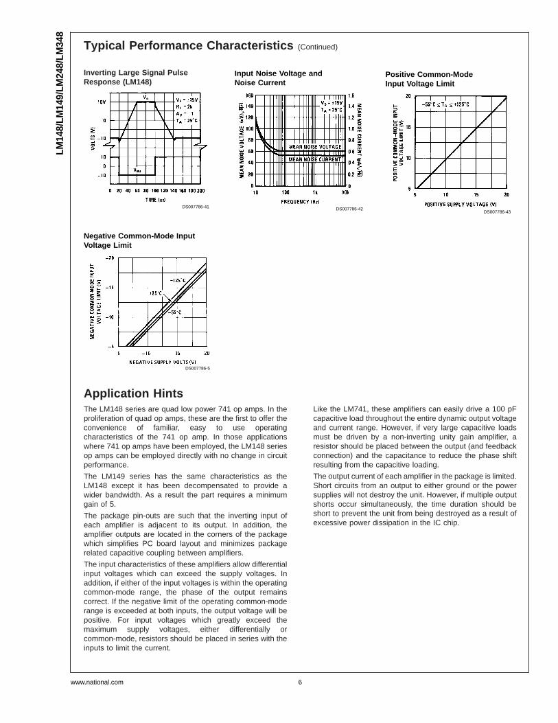
Application HintsThe LM148 series are quad low power 741 op amps. In theproliferation of quad op amps, these are the first to offer theconvenience of familiar, easy to use operatingcharacteristics of the 741 op amp. In those applicationswhere 741 op amps have been employed, the LM148 seriesop amps can be employed directly with no change in circuitperformance.
The LM149 series has the same characteristics as theLM148 except it has been decompensated to provide awider bandwidth. As a result the part requires a minimumgain of 5.
The package pin-outs are such that the inverting input ofeach amplifier is adjacent to its output. In addition, theamplifier outputs are located in the corners of the packagewhich simplifies PC board layout and minimizes packagerelated capacitive coupling between amplifiers.
The input characteristics of these amplifiers allow differentialinput voltages which can exceed the supply voltages. Inaddition, if either of the input voltages is within the operatingcommon-mode range, the phase of the output remainscorrect. If the negative limit of the operating common-moderange is exceeded at both inputs, the output voltage will bepositive. For input voltages which greatly exceed themaximum supply voltages, either differentially orcommon-mode, resistors should be placed in series with theinputs to limit the current.
Like the LM741, these amplifiers can easily drive a 100 pFcapacitive load throughout the entire dynamic output voltageand current range. However, if very large capacitive loadsmust be driven by a non-inverting unity gain amplifier, aresistor should be placed between the output (and feedbackconnection) and the capacitance to reduce the phase shiftresulting from the capacitive loading.
The output current of each amplifier in the package is limited.Short circuits from an output to either ground or the powersupplies will not destroy the unit. However, if multiple outputshorts occur simultaneously, the time duration should beshort to prevent the unit from being destroyed as a result ofexcessive power dissipation in the IC chip.
Inverting Large Signal PulseResponse (LM148)
DS007786-41
Input Noise Voltage andNoise Current
DS007786-42
Positive Common-ModeInput Voltage Limit
DS007786-43
Negative Common-Mode InputVoltage Limit
DS007786-5
LM14
8/LM
149/
LM24
8/LM
348
www.national.com 6

Application Hints (Continued)
As with most amplifiers, care should be taken lead dress,component placement and supply decoupling in order toensure stability. For example, resistors from the output to aninput should be placed with the body close to the input tominimize “pickup” and maximize the frequency of thefeedback pole which capacitance from the input to groundcreates.
A feedback pole is created when the feedback around anyamplifier is resistive. The parallel resistance and capacitance
from the input of the device (usually the inverting input) to ACground set the frequency of the pole. In many instances thefrequency of this pole is much greater than the expected 3dB frequency of the closed loop gain and consequently thereis negligible effect on stability margin. However, if thefeedback pole is less than approximately six times theexpected 3 dB frequency a lead capacitor should be placedfrom the output to the input of the op amp. The value of theadded capacitor should be such that the RC time constant ofthis capacitor and the resistance it parallels is greater than orequal to the original feedback pole time constant.
Typical Applications—LM148
One Decade Low Distortion Sinewave Generator
DS007786-8
fMAX = 5 kHz, THD ≤ 0.03%R1 = 100k pot. C1 = 0.0047 µF, C2 = 0.01 µF, C3 = 0.1 µF, R2 = R6 = R7 = 1M,R3 = 5.1k, R4 = 12Ω, R5 = 240Ω, Q = NS5102, D1 = 1N914, D2 = 3.6V avalanchediode (ex. LM103), VS = ±15VA simpler version with some distortion degradation at high frequencies can be made by using A1 as a simple inverting amplifier, and by putting back to backzeners in the feedback loop of A3.
LM148/LM
149/LM248/LM
348
www.national.com7
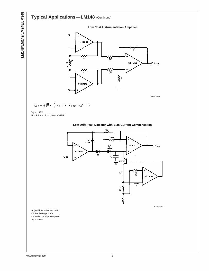
Typical Applications—LM148 (Continued)
Low Cost Instrumentation Amplifier
DS007786-9
VS = ±15VR = R2, trim R2 to boost CMRR
Low Drift Peak Detector with Bias Current Compensation
DS007786-10
Adjust R for minimum driftD3 low leakage diodeD1 added to improve speedVS = ±15V
LM14
8/LM
149/
LM24
8/LM
348
www.national.com 8

Typical Applications—LM148 (Continued)
Universal State-Variable Filter
DS007786-11
Tune Q through R0,For predictable results: fO Q ≤ 4 x 10⁴
Use Band Pass output to tune for Q
LM148/LM
149/LM248/LM
348
www.national.com9

Typical Applications—LM148 (Continued)
A 1 kHz 4 Pole Butterworth
DS007786-12
Use general equations, and tune each section separatelyQ1stSECTION = 0.541, Q2ndSECTION = 1.306The response should have 0 dB peaking
A 3 Amplifier Bi-Quad Notch Filter
DS007786-13
Ex: fNOTCH = 3 kHz, Q = 5, R1 = 270k, R2 = R3 = 20k, R4 = 27k, R5 = 20k, R6 = R8 = 10k, R7 = 100k, C1 = C2 = 0.001 µFBetter noise performance than the state-space approach.
LM14
8/LM
149/
LM24
8/LM
348
www.national.com 10

Typical Applications—LM148 (Continued)
A 4th Order 1 kHz Elliptic Filter (4 Poles, 4 Zeros)
DS007786-14
R1C1 = R2C2 = tR'1C'1 = R'2C'2 = t'fC = 1 kHz, fS = 2 kHz, fp = 0.543, fZ = 2.14, Q = 0.841, f' P = 0.987, f' Z = 4.92, Q' = 4.403, normalized to ripple BW
Use the BP outputs to tune Q, Q', tune the 2 sections separatelyR1 = R2 = 92.6k, R3 = R4 = R5 = 100k, R6 = 10k, R0 = 107.8k, RL = 100k, RH = 155.1k,R'1 = R'2 = 50.9k, R'4 = R'5 = 100k, R'6 = 10k, R'0 = 5.78k, R'L = 100k, R'H = 248.12k, R'f = 100k. All capacitors are 0.001 µF.
Lowpass Response
DS007786-15
LM148/LM
149/LM248/LM
348
www.national.com11
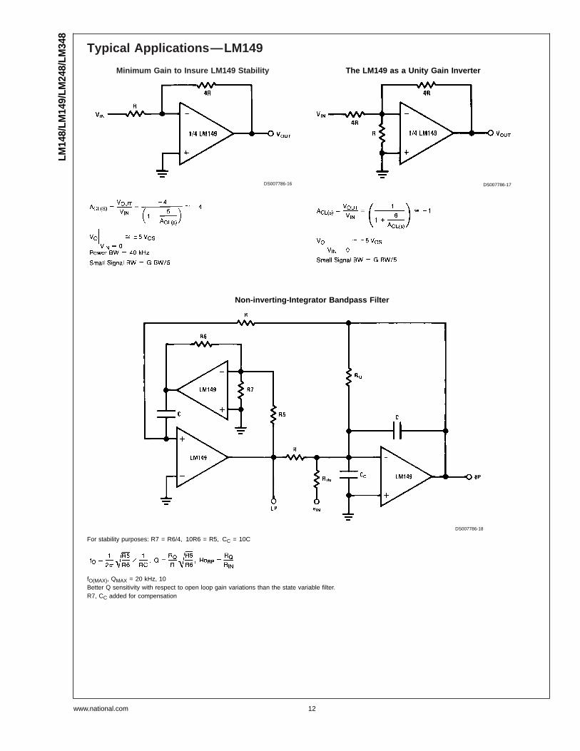
Typical Applications—LM149
Minimum Gain to Insure LM149 Stability
DS007786-16
The LM149 as a Unity Gain Inverter
DS007786-17
Non-inverting-Integrator Bandpass Filter
DS007786-18
For stability purposes: R7 = R6/4, 10R6 = R5, CC = 10C
fO(MAX), QMAX = 20 kHz, 10Better Q sensitivity with respect to open loop gain variations than the state variable filter.R7, CC added for compensation
LM14
8/LM
149/
LM24
8/LM
348
www.national.com 12

Typical Applications—LM149 (Continued)
Active Tone Control with Full Output Swing (No Slew Limiting at 20 kHz)
DS007786-19
VS = ±15V, VOUT(MAX) = 9.1 VRMS,fMAX = 20 kHz, THD ≤ 1%Duplicate the above circuit for stereo
Max Bass Gain . (R1 + R2)/R1Max Treble Gain . (R1 + 2R7)/R5as shown: fL . 32 Hz, fLB . 320 HzfH . 11 kHz, fHB . 1.1 Hz
LM148/LM
149/LM248/LM
348
www.national.com13

Typical Applications—LM149 (Continued)
Triangular Squarewave Generator
DS007786-20
Use LM125 for ±15V supplyThe circuit can be used as a low frequency V/F for process control.Q1, Q3: KE4393, Q2, Q4: P1087E, D1–D4 = 1N914
LM14
8/LM
149/
LM24
8/LM
348
www.national.com 14

Typical Simulation
LM148, LM149, LM741 Macromodel for Computer Simulation
DS007786-21
For more details, see IEEE Journal of Solid-State Circuits, Vol. SC-9, No. 6, December 1974
Note 6: o1 = 112IS = 8 x 10⁻¹⁶
Note 7: o2 = 144*C2 = 6 pF for LM149
DS007786-22
LM148/LM
149/LM248/LM
348
www.national.com15

Connection Diagram
DS007786-2
Top ViewOrder Number LM148J, LM148J/883, LM149J/883, LM248J, LM348M, or LM348N
See NS Package Number J14A, M14A or N14ALM148J is available per JM38510/11001
LM14
8/LM
149/
LM24
8/LM
348
www.national.com 16

Physical Dimensions inches (millimeters) unless otherwise noted
Ceramic Dual-In-Line Package (J)Order Number LM148J, LM148J/883, LM149J/883, LM248J
NS Package Number J14A
S.O. Package (M)Order Number LM348M or LM348MX
NS Package Number M14A
LM148/LM
149/LM248/LM
348
www.national.com17

Physical Dimensions inches (millimeters) unless otherwise noted (Continued)
LIFE SUPPORT POLICY
NATIONAL’S PRODUCTS ARE NOT AUTHORIZED FOR USE AS CRITICAL COMPONENTS IN LIFE SUPPORTDEVICES OR SYSTEMS WITHOUT THE EXPRESS WRITTEN APPROVAL OF THE PRESIDENT AND GENERALCOUNSEL OF NATIONAL SEMICONDUCTOR CORPORATION. As used herein:
1. Life support devices or systems are devices orsystems which, (a) are intended for surgical implantinto the body, or (b) support or sustain life, andwhose failure to perform when properly used inaccordance with instructions for use provided in thelabeling, can be reasonably expected to result in asignificant injury to the user.
2. A critical component is any component of a lifesupport device or system whose failure to performcan be reasonably expected to cause the failure ofthe life support device or system, or to affect itssafety or effectiveness.
National SemiconductorCorporationAmericasTel: 1-800-272-9959Fax: 1-800-737-7018Email: [email protected]
National SemiconductorEurope
Fax: +49 (0) 180-530 85 86Email: [email protected]
Deutsch Tel: +49 (0) 69 9508 6208English Tel: +44 (0) 870 24 0 2171Français Tel: +33 (0) 1 41 91 8790
National SemiconductorAsia Pacific CustomerResponse GroupTel: 65-2544466Fax: 65-2504466Email: [email protected]
National SemiconductorJapan Ltd.Tel: 81-3-5639-7560Fax: 81-3-5639-7507
www.national.com
Molded Dual-In-Line Package (N)Order Number LM348N
NS Package Number N14A
LM14
8/LM
149
Ser
ies
Qua
d74
1O
pA
mp
National does not assume any responsibility for use of any circuitry described, no circuit patent licenses are implied and National reserves the right at any time without notice to change said circuitry and specifications.