Embed Size (px)
Citation preview
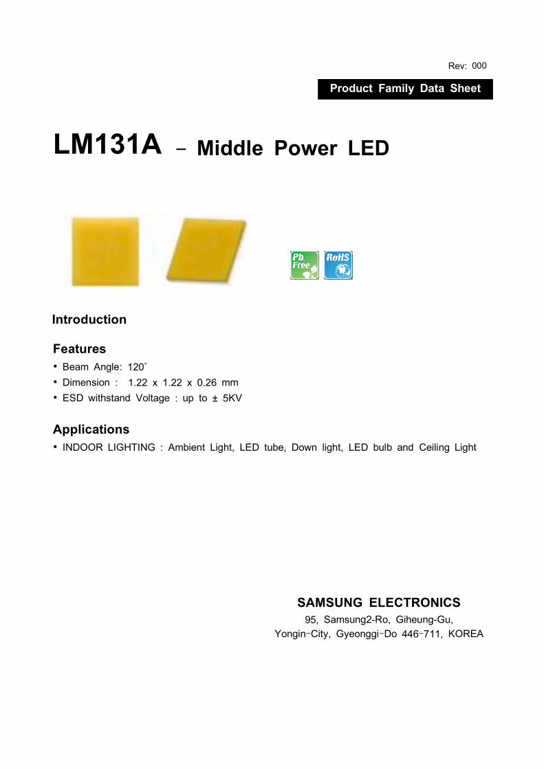
Rev:
Product Family Data Sheet
SAMSUNG ELECTRONICS95, Samsung2-Ro, Giheung-Gu,
Yongin-City, Gyeonggi-Do 446-711, KOREA
000
LM131A - Middle Power LED
Introduction
Features Beam Angle: 120˚ Dimension : 1.22 x 1.22 x 0.26 mm ESD withstand Voltage : up to ± 5KV
Applications INDOOR LIGHTING : Ambient Light, LED tube, Down light, LED bulb and Ceiling Light
http://www.samsungled.com 2 / 30
Contents
1. Product Code Information ----------------------- 3
2. Characteristics ----------------------- 11
3. Typical Characteristics Graph ----------------------- 12
4. Outline Drawing & Dimension ----------------------- 14
5. Reliability Test Items & Conditions ----------------------- 16
6. Solder Conditions ----------------------- 17
7. Tape & Reel ----------------------- 18
8. Label Structure ----------------------- 20
9. Packing Structure ----------------------- 21
10. Precaution For Use ----------------------- 23
11. Hazard Substance Analysis Report ----------------------- 25
Revision History ----------------------- 31
http://www.samsungled.com 3 / 30
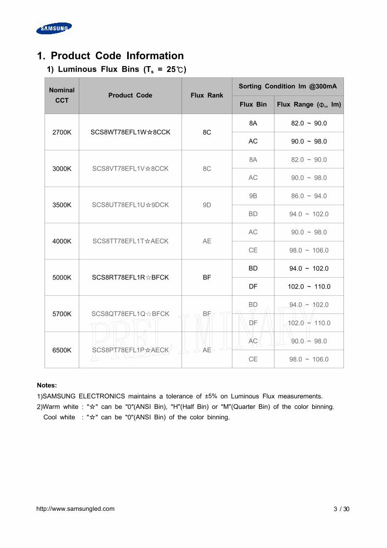
1. Product Code Information1) Luminous Flux Bins (Ts = 25℃)
NominalCCT
Product Code Flux RankSorting Condition lm @300mA
Flux Bin Flux Range (Φv, lm)
2700K SCS8WT78EFL1W☆8CCK 8C8A 82.0 ~ 90.0
AC 90.0 ~ 98.0
3000K SCS8VT78EFL1V☆8CCK 8C8A 82.0 ~ 90.0
AC 90.0 ~ 98.0
3500K SCS8UT78EFL1U☆9DCK 9D9B 86.0 ~ 94.0
BD 94.0 ~ 102.0
4000K SCS8TT78EFL1T☆AECK AEAC 90.0 ~ 98.0
CE 98.0 ~ 106.0
5000K SCS8RT78EFL1R☆BFCK BFBD 94.0 ~ 102.0
DF 102.0 ~ 110.0
5700K SCS8QT78EFL1Q☆BFCK BFBD 94.0 ~ 102.0
DF 102.0 ~ 110.0
6500K SCS8PT78EFL1P☆AECK AEAC 90.0 ~ 98.0
CE 98.0 ~ 106.0
Notes:1)SAMSUNG ELECTRONICS maintains a tolerance of ±5% on Luminous Flux measurements.2)Warm white : "☆" can be "0"(ANSI Bin), "H"(Half Bin) or "M"(Quarter Bin) of the color binning.Cool white : "☆" can be "0"(ANSI Bin) of the color binning.
http://www.samsungled.com 4 / 30
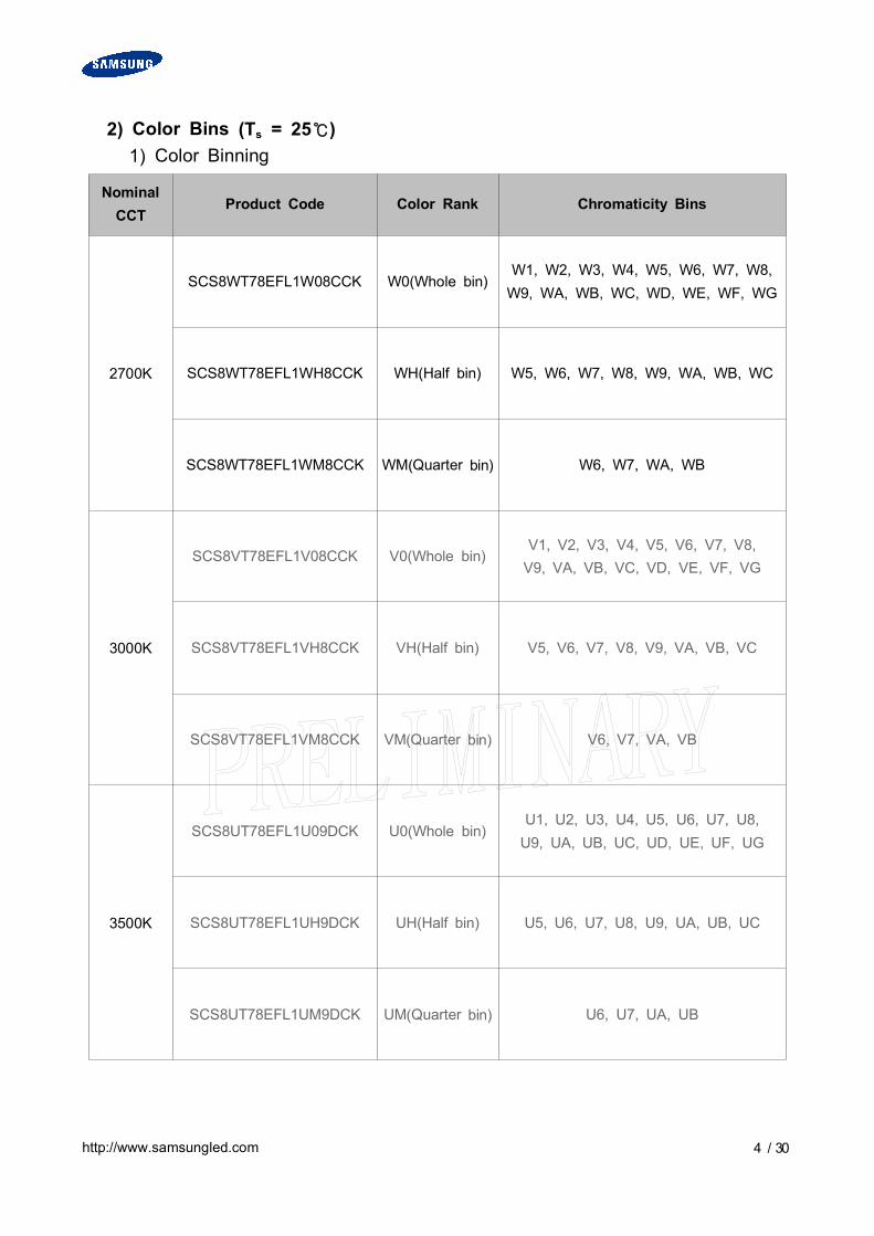
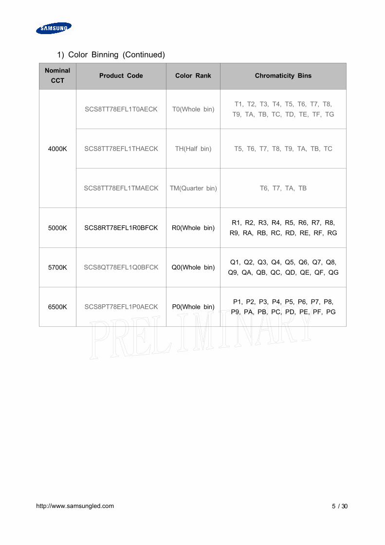
2) Color Bins (Ts = 25℃)1) Color Binning
NominalCCT
Product Code Color Rank Chromaticity Bins
2700K
SCS8WT78EFL1W08CCK W0(Whole bin)W1, W2, W3, W4, W5, W6, W7, W8,W9, WA, WB, WC, WD, WE, WF, WG
SCS8WT78EFL1WH8CCK WH(Half bin) W5, W6, W7, W8, W9, WA, WB, WC
SCS8WT78EFL1WM8CCK WM(Quarter bin) W6, W7, WA, WB
3000K
SCS8VT78EFL1V08CCK V0(Whole bin)V1, V2, V3, V4, V5, V6, V7, V8,V9, VA, VB, VC, VD, VE, VF, VG
SCS8VT78EFL1VH8CCK VH(Half bin) V5, V6, V7, V8, V9, VA, VB, VC
SCS8VT78EFL1VM8CCK VM(Quarter bin) V6, V7, VA, VB
3500K
SCS8UT78EFL1U09DCK U0(Whole bin)U1, U2, U3, U4, U5, U6, U7, U8,U9, UA, UB, UC, UD, UE, UF, UG
SCS8UT78EFL1UH9DCK UH(Half bin) U5, U6, U7, U8, U9, UA, UB, UC
SCS8UT78EFL1UM9DCK UM(Quarter bin) U6, U7, UA, UB
http://www.samsungled.com 5 / 30
1) Color Binning (Continued)
NominalCCT
Product Code Color Rank Chromaticity Bins
4000K
SCS8TT78EFL1T0AECK T0(Whole bin)T1, T2, T3, T4, T5, T6, T7, T8,T9, TA, TB, TC, TD, TE, TF, TG
SCS8TT78EFL1THAECK TH(Half bin) T5, T6, T7, T8, T9, TA, TB, TC
SCS8TT78EFL1TMAECK TM(Quarter bin) T6, T7, TA, TB
5000K SCS8RT78EFL1R0BFCK R0(Whole bin)R1, R2, R3, R4, R5, R6, R7, R8,R9, RA, RB, RC, RD, RE, RF, RG
5700K SCS8QT78EFL1Q0BFCK Q0(Whole bin)Q1, Q2, Q3, Q4, Q5, Q6, Q7, Q8,Q9, QA, QB, QC, QD, QE, QF, QG
6500K SCS8PT78EFL1P0AECK P0(Whole bin)P1, P2, P3, P4, P5, P6, P7, P8,P9, PA, PB, PC, PD, PE, PF, PG
http://www.samsungled.com 6 / 30
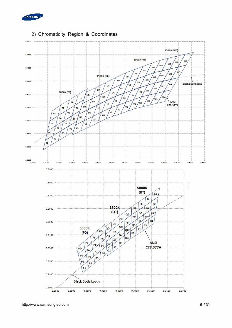
2) Chromaticity Region & Coordinates
http://www.samsungled.com 7 / 30
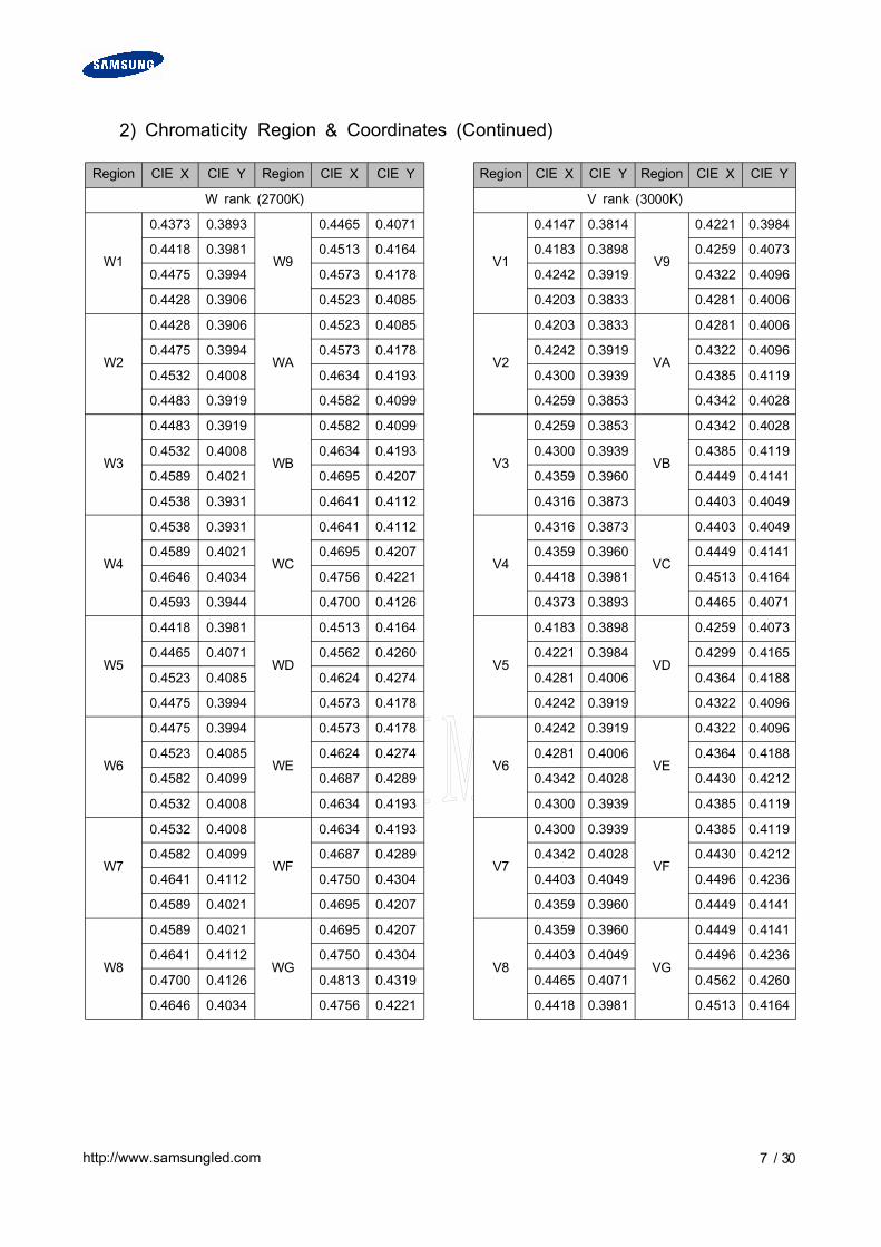
2) Chromaticity Region & Coordinates (Continued)
Region CIE X CIE Y Region CIE X CIE Y
V rank (3000K)
V1
0.4147 0.3814
V9
0.4221 0.3984
0.4183 0.3898 0.4259 0.4073
0.4242 0.3919 0.4322 0.4096
0.4203 0.3833 0.4281 0.4006
V2
0.4203 0.3833
VA
0.4281 0.4006
0.4242 0.3919 0.4322 0.4096
0.4300 0.3939 0.4385 0.4119
0.4259 0.3853 0.4342 0.4028
V3
0.4259 0.3853
VB
0.4342 0.4028
0.4300 0.3939 0.4385 0.4119
0.4359 0.3960 0.4449 0.4141
0.4316 0.3873 0.4403 0.4049
V4
0.4316 0.3873
VC
0.4403 0.4049
0.4359 0.3960 0.4449 0.4141
0.4418 0.3981 0.4513 0.4164
0.4373 0.3893 0.4465 0.4071
V5
0.4183 0.3898
VD
0.4259 0.4073
0.4221 0.3984 0.4299 0.4165
0.4281 0.4006 0.4364 0.4188
0.4242 0.3919 0.4322 0.4096
V6
0.4242 0.3919
VE
0.4322 0.4096
0.4281 0.4006 0.4364 0.4188
0.4342 0.4028 0.4430 0.4212
0.4300 0.3939 0.4385 0.4119
V7
0.4300 0.3939
VF
0.4385 0.4119
0.4342 0.4028 0.4430 0.4212
0.4403 0.4049 0.4496 0.4236
0.4359 0.3960 0.4449 0.4141
V8
0.4359 0.3960
VG
0.4449 0.4141
0.4403 0.4049 0.4496 0.4236
0.4465 0.4071 0.4562 0.4260
0.4418 0.3981 0.4513 0.4164
Region CIE X CIE Y Region CIE X CIE Y
W rank (2700K)
W1
0.4373 0.3893
W9
0.4465 0.4071
0.4418 0.3981 0.4513 0.4164
0.4475 0.3994 0.4573 0.4178
0.4428 0.3906 0.4523 0.4085
W2
0.4428 0.3906
WA
0.4523 0.4085
0.4475 0.3994 0.4573 0.4178
0.4532 0.4008 0.4634 0.4193
0.4483 0.3919 0.4582 0.4099
W3
0.4483 0.3919
WB
0.4582 0.4099
0.4532 0.4008 0.4634 0.4193
0.4589 0.4021 0.4695 0.4207
0.4538 0.3931 0.4641 0.4112
W4
0.4538 0.3931
WC
0.4641 0.4112
0.4589 0.4021 0.4695 0.4207
0.4646 0.4034 0.4756 0.4221
0.4593 0.3944 0.4700 0.4126
W5
0.4418 0.3981
WD
0.4513 0.4164
0.4465 0.4071 0.4562 0.4260
0.4523 0.4085 0.4624 0.4274
0.4475 0.3994 0.4573 0.4178
W6
0.4475 0.3994
WE
0.4573 0.4178
0.4523 0.4085 0.4624 0.4274
0.4582 0.4099 0.4687 0.4289
0.4532 0.4008 0.4634 0.4193
W7
0.4532 0.4008
WF
0.4634 0.4193
0.4582 0.4099 0.4687 0.4289
0.4641 0.4112 0.4750 0.4304
0.4589 0.4021 0.4695 0.4207
W8
0.4589 0.4021
WG
0.4695 0.4207
0.4641 0.4112 0.4750 0.4304
0.4700 0.4126 0.4813 0.4319
0.4646 0.4034 0.4756 0.4221

http://www.samsungled.com 8 / 30
2) Chromaticity Region & Coordinates (Continued)
Region CIE X CIE Y Region CIE X CIE Y
T rank (4000K)
T1
0.367 0.3578
T9
0.3702 0.3722
0.3726 0.3612 0.3763 0.376
0.3744 0.3685 0.3782 0.3837
0.3686 0.3649 0.3719 0.3797
T2
0.3726 0.3612
TA
0.3763 0.3760
0.3783 0.3646 0.3825 0.3798
0.3804 0.3721 0.3847 0.3877
0.3744 0.3685 0.3782 0.3837
T3
0.3783 0.3646
TB
0.3825 0.3798
0.3840 0.3681 0.3887 0.3836
0.3863 0.3758 0.3912 0.3917
0.3804 0.3721 0.3847 0.3877
T4
0.384 0.3681
TC
0.3887 0.3837
0.3898 0.3716 0.395 0.3875
0.3924 0.3794 0.3978 0.3958
0.3863 0.3758 0.3912 0.3917
T5
0.3686 0.3649
TD
0.3719 0.3797
0.3744 0.3685 0.3782 0.3837
0.3763 0.376 0.3802 0.3916
0.3702 0.3722 0.3736 0.3874
T6
0.3744 0.3685
TE
0.3782 0.3837
0.3804 0.3721 0.3847 0.3877
0.3825 0.3798 0.3869 0.3958
0.3763 0.376 0.3802 0.3916
T7
0.3804 0.3721
TF
0.3847 0.3877
0.3863 0.3758 0.3912 0.3917
0.3887 0.3836 0.3937 0.4001
0.3825 0.3798 0.3869 0.3958
T8
0.3863 0.3758
TG
0.3912 0.3917
0.3924 0.3794 0.3978 0.3958
0.395 0.3875 0.4006 0.4044
0.3887 0.3836 0.3937 0.4001
Region CIE X CIE Y Region CIE X CIE Y
U rank (3500K)
U1
0.3889 0.3690
U9
0.3941 0.3848
0.3915 0.3768 0.3968 0.3930
0.3981 0.3800 0.4040 0.3966
0.3953 0.3720 0.4010 0.3882
U2
0.3953 0.3720
UA
0.4010 0.3882
0.3981 0.3800 0.4040 0.3966
0.4048 0.3832 0.4113 0.4001
0.4017 0.3751 0.4080 0.3916
U3
0.4017 0.3751
UB
0.4080 0.3916
0.4048 0.3832 0.4113 0.4001
0.4116 0.3865 0.4186 0.4037
0.4082 0.3782 0.4150 0.3950
U4
0.4082 0.3782
UC
0.4150 0.3950
0.4116 0.3865 0.4186 0.4037
0.4183 0.3898 0.4259 0.4073
0.4147 0.3814 0.4221 0.3984
U5
0.3915 0.3768
UD
0.3968 0.3930
0.3941 0.3848 0.3996 0.4015
0.4010 0.3882 0.4071 0.4052
0.3981 0.3800 0.4040 0.3966
U6
0.3981 0.3800
UE
0.4040 0.3966
0.4010 0.3882 0.4071 0.4052
0.4080 0.3916 0.4146 0.4089
0.4048 0.3832 0.4113 0.4001
U7
0.4048 0.3832
UF
0.4113 0.4001
0.4080 0.3916 0.4146 0.4089
0.4150 0.3950 0.4222 0.4127
0.4116 0.3865 0.4186 0.4037
U8
0.4116 0.3865
UG
0.4186 0.4037
0.4150 0.3950 0.4222 0.4127
0.4221 0.3984 0.4299 0.4165
0.4183 0.3898 0.4259 0.4073
http://www.samsungled.com 9 / 30
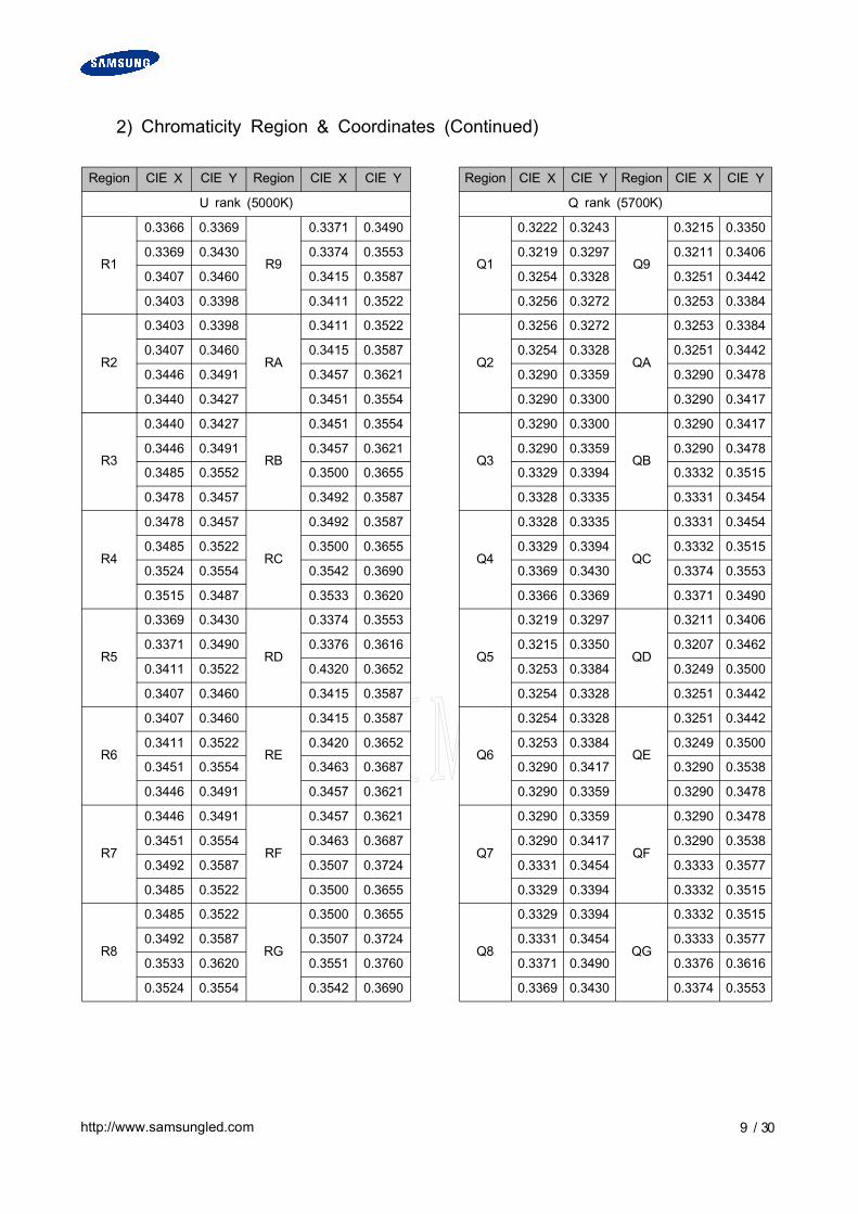
2) Chromaticity Region & Coordinates (Continued)
Region CIE X CIE Y Region CIE X CIE Y
U rank (5000K)
R1
0.3366 0.3369
R9
0.3371 0.3490
0.3369 0.3430 0.3374 0.3553
0.3407 0.3460 0.3415 0.3587
0.3403 0.3398 0.3411 0.3522
R2
0.3403 0.3398
RA
0.3411 0.3522
0.3407 0.3460 0.3415 0.3587
0.3446 0.3491 0.3457 0.3621
0.3440 0.3427 0.3451 0.3554
R3
0.3440 0.3427
RB
0.3451 0.3554
0.3446 0.3491 0.3457 0.3621
0.3485 0.3552 0.3500 0.3655
0.3478 0.3457 0.3492 0.3587
R4
0.3478 0.3457
RC
0.3492 0.3587
0.3485 0.3522 0.3500 0.3655
0.3524 0.3554 0.3542 0.3690
0.3515 0.3487 0.3533 0.3620
R5
0.3369 0.3430
RD
0.3374 0.3553
0.3371 0.3490 0.3376 0.3616
0.3411 0.3522 0.4320 0.3652
0.3407 0.3460 0.3415 0.3587
R6
0.3407 0.3460
RE
0.3415 0.3587
0.3411 0.3522 0.3420 0.3652
0.3451 0.3554 0.3463 0.3687
0.3446 0.3491 0.3457 0.3621
R7
0.3446 0.3491
RF
0.3457 0.3621
0.3451 0.3554 0.3463 0.3687
0.3492 0.3587 0.3507 0.3724
0.3485 0.3522 0.3500 0.3655
R8
0.3485 0.3522
RG
0.3500 0.3655
0.3492 0.3587 0.3507 0.3724
0.3533 0.3620 0.3551 0.3760
0.3524 0.3554 0.3542 0.3690
Region CIE X CIE Y Region CIE X CIE Y
Q rank (5700K)
Q1
0.3222 0.3243
Q9
0.3215 0.3350
0.3219 0.3297 0.3211 0.3406
0.3254 0.3328 0.3251 0.3442
0.3256 0.3272 0.3253 0.3384
Q2
0.3256 0.3272
QA
0.3253 0.3384
0.3254 0.3328 0.3251 0.3442
0.3290 0.3359 0.3290 0.3478
0.3290 0.3300 0.3290 0.3417
Q3
0.3290 0.3300
QB
0.3290 0.3417
0.3290 0.3359 0.3290 0.3478
0.3329 0.3394 0.3332 0.3515
0.3328 0.3335 0.3331 0.3454
Q4
0.3328 0.3335
QC
0.3331 0.3454
0.3329 0.3394 0.3332 0.3515
0.3369 0.3430 0.3374 0.3553
0.3366 0.3369 0.3371 0.3490
Q5
0.3219 0.3297
QD
0.3211 0.3406
0.3215 0.3350 0.3207 0.3462
0.3253 0.3384 0.3249 0.3500
0.3254 0.3328 0.3251 0.3442
Q6
0.3254 0.3328
QE
0.3251 0.3442
0.3253 0.3384 0.3249 0.3500
0.3290 0.3417 0.3290 0.3538
0.3290 0.3359 0.3290 0.3478
Q7
0.3290 0.3359
QF
0.3290 0.3478
0.3290 0.3417 0.3290 0.3538
0.3331 0.3454 0.3333 0.3577
0.3329 0.3394 0.3332 0.3515
Q8
0.3329 0.3394
QG
0.3332 0.3515
0.3331 0.3454 0.3333 0.3577
0.3371 0.3490 0.3376 0.3616
0.3369 0.3430 0.3374 0.3553
http://www.samsungled.com 10 / 30
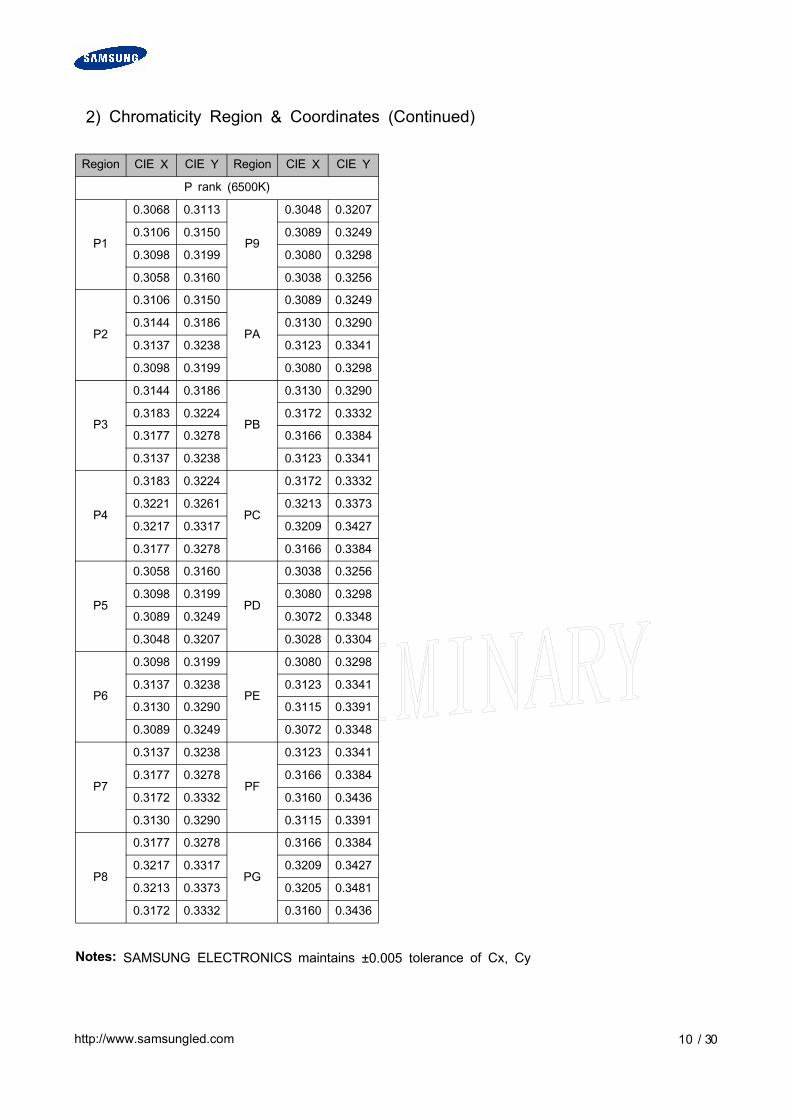
2) Chromaticity Region & Coordinates (Continued)
Region CIE X CIE Y Region CIE X CIE Y
P rank (6500K)
P1
0.3068 0.3113
P9
0.3048 0.3207
0.3106 0.3150 0.3089 0.3249
0.3098 0.3199 0.3080 0.3298
0.3058 0.3160 0.3038 0.3256
P2
0.3106 0.3150
PA
0.3089 0.3249
0.3144 0.3186 0.3130 0.3290
0.3137 0.3238 0.3123 0.3341
0.3098 0.3199 0.3080 0.3298
P3
0.3144 0.3186
PB
0.3130 0.3290
0.3183 0.3224 0.3172 0.3332
0.3177 0.3278 0.3166 0.3384
0.3137 0.3238 0.3123 0.3341
P4
0.3183 0.3224
PC
0.3172 0.3332
0.3221 0.3261 0.3213 0.3373
0.3217 0.3317 0.3209 0.3427
0.3177 0.3278 0.3166 0.3384
P5
0.3058 0.3160
PD
0.3038 0.3256
0.3098 0.3199 0.3080 0.3298
0.3089 0.3249 0.3072 0.3348
0.3048 0.3207 0.3028 0.3304
P6
0.3098 0.3199
PE
0.3080 0.3298
0.3137 0.3238 0.3123 0.3341
0.3130 0.3290 0.3115 0.3391
0.3089 0.3249 0.3072 0.3348
P7
0.3137 0.3238
PF
0.3123 0.3341
0.3177 0.3278 0.3166 0.3384
0.3172 0.3332 0.3160 0.3436
0.3130 0.3290 0.3115 0.3391
P8
0.3177 0.3278
PG
0.3166 0.3384
0.3217 0.3317 0.3209 0.3427
0.3213 0.3373 0.3205 0.3481
0.3172 0.3332 0.3160 0.3436
Notes: SAMSUNG ELECTRONICS maintains ±0.005 tolerance of Cx, Cy
http://www.samsungled.com 11 / 30
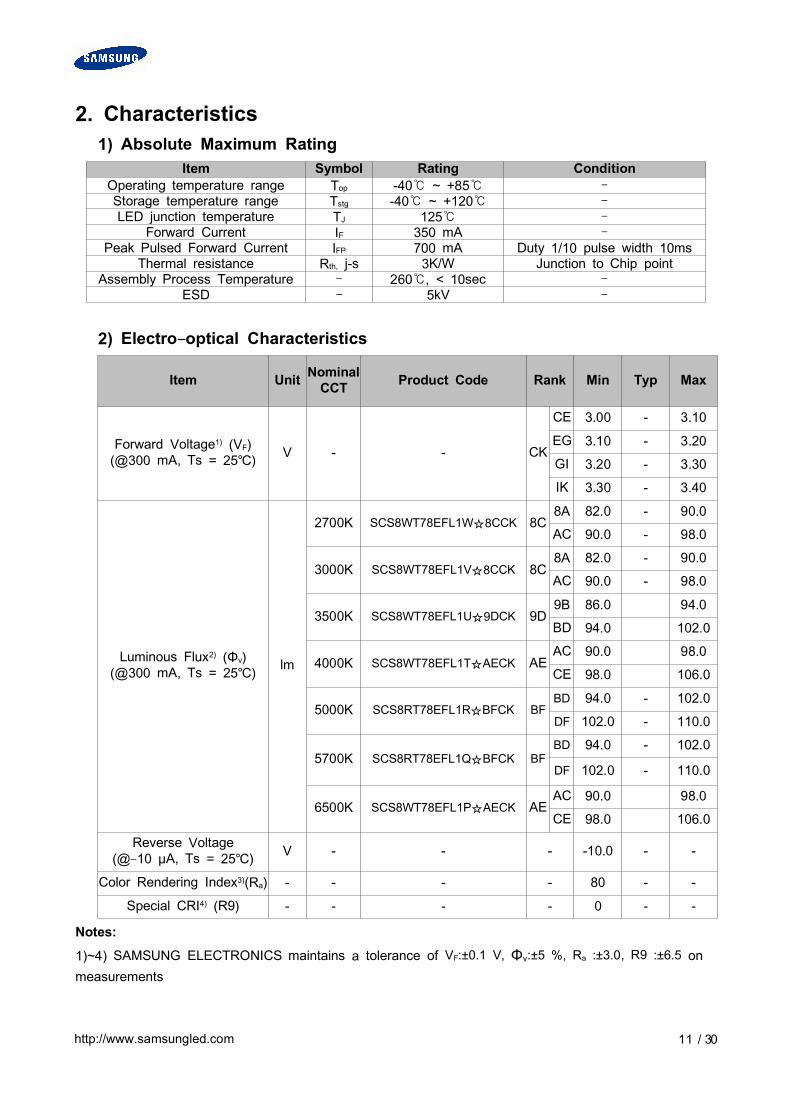
2. Characteristics1) Absolute Maximum Rating
Item Symbol Rating ConditionOperating temperature range Top -40℃ ~ +85℃ -Storage temperature range Tstg -40℃ ~ +120℃ -LED junction temperature TJ 125℃ -
Forward Current IF 350 mA -Peak Pulsed Forward Current IFP 700 mA Duty 1/10 pulse width 10ms
Thermal resistance Rth, j-s 3K/W Junction to Chip pointAssembly Process Temperature - 260℃, < 10sec -
ESD - 5kV -
2) Electro-optical Characteristics
Item Unit NominalCCT Product Code Rank Min Typ Max
Forward Voltage1) (VF)(@300 mA, Ts = 25℃) V - - CK
CE 3.00 - 3.10EG 3.10 - 3.20GI 3.20 - 3.30IK 3.30 - 3.40
Luminous Flux2) (Φv)(@300 mA, Ts = 25℃) lm
2700K SCS8WT78EFL1W☆8CCK 8C8A 82.0 - 90.0AC 90.0 - 98.0
3000K SCS8WT78EFL1V☆8CCK 8C8A 82.0 - 90.0AC 90.0 - 98.0
3500K SCS8WT78EFL1U☆9DCK 9D9B 86.0 94.0BD 94.0 102.0
4000K SCS8WT78EFL1T☆AECK AEAC 90.0 98.0CE 98.0 106.0
5000K SCS8RT78EFL1R☆BFCK BFBD 94.0 - 102.0DF 102.0 - 110.0
5700K SCS8RT78EFL1Q☆BFCK BFBD 94.0 - 102.0
DF 102.0 - 110.0
6500K SCS8WT78EFL1P☆AECK AEAC 90.0 98.0CE 98.0 106.0
Reverse Voltage(@-10 μA, Ts = 25℃) V - - - -10.0 - -
Color Rendering Index3)(Ra) - - - - 80 - -Special CRI4) (R9) - - - - 0 - -
Notes:
1)~4) SAMSUNG ELECTRONICS maintains a tolerance of VF:±0.1 V, Φv:±5 %, Ra :±3.0, R9 :±6.5 onmeasurements
http://www.samsungled.com 12 / 30
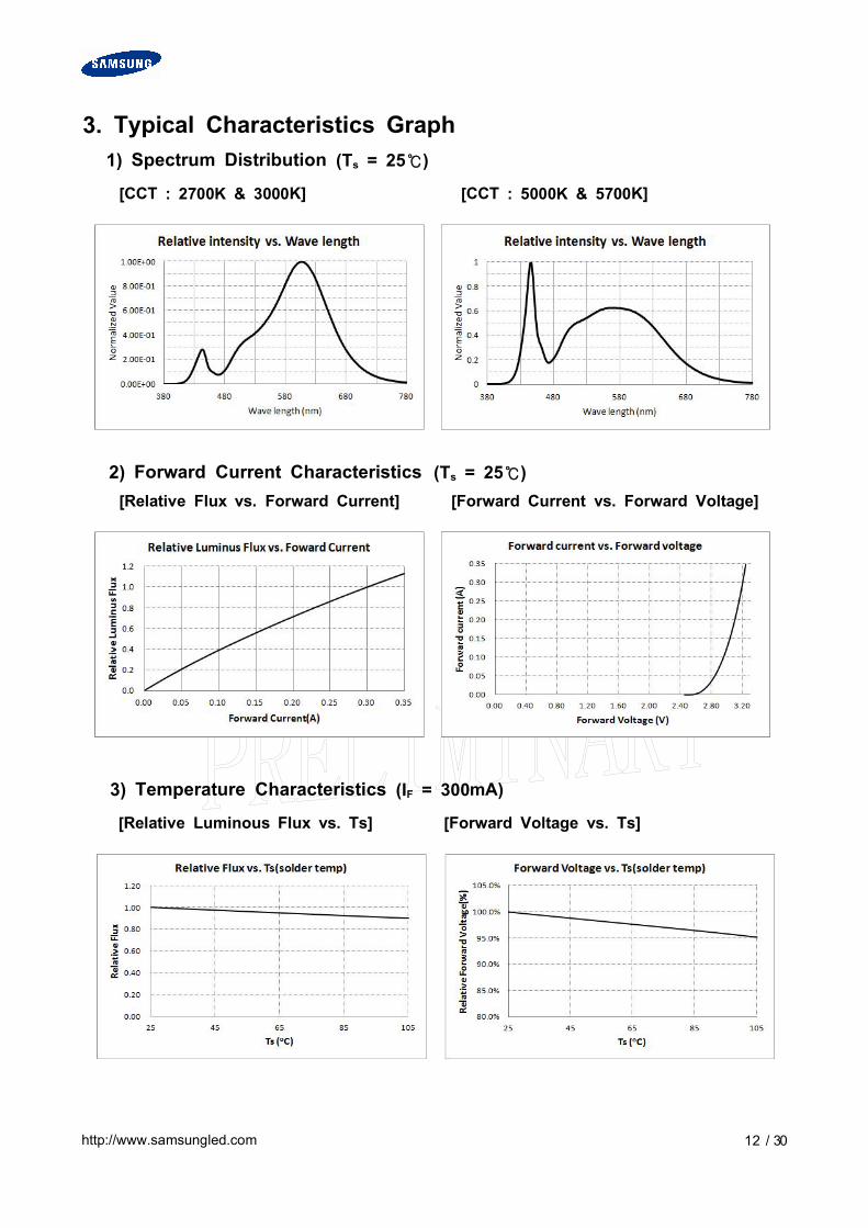
3. Typical Characteristics Graph1) Spectrum Distribution (Ts = 25℃)
[CCT : 2700K & 3000K] [CCT : 5000K & 5700K]
2) Forward Current Characteristics (Ts = 25℃)[Relative Flux vs. Forward Current] [Forward Current vs. Forward Voltage]
3) Temperature Characteristics (IF = 300mA)
[Relative Luminous Flux vs. Ts] [Forward Voltage vs. Ts]
http://www.samsungled.com 13 / 30
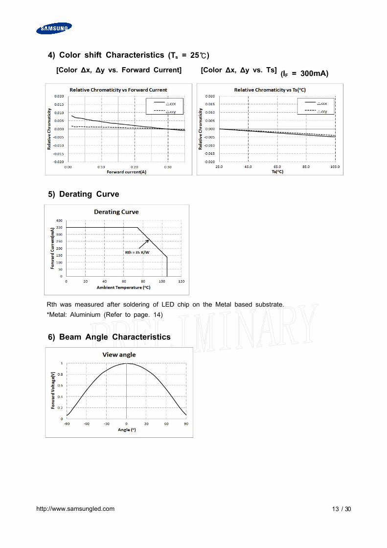
4) Color shift Characteristics (Ts = 25℃)
[Color Δx, Δy vs. Forward Current] [Color Δx, Δy vs. Ts] (IF = 300mA)
5) Derating Curve
Rth was measured after soldering of LED chip on the Metal based substrate.*Metal: Aluminium (Refer to page. 14)
6) Beam Angle Characteristics
http://www.samsungled.com 14 / 30
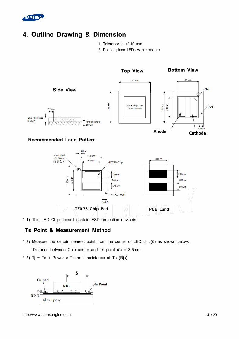
4. Outline Drawing & Dimension
Recommended Land Pattern
* 1) This LED Chip doesn't contain ESD protection device(s).
Ts Point & Measurement Method
* 2) Measure the certain nearest point from the center of LED chip(δ) as shown below.
Distance between Chip center and Ts point (δ) = 3.5mm
* 3) Tj = Ts + Power x Thermal resistance at Ts (Rjs)
1. Tolerance is ±0.10 mm2. Do not place LEDs with pressure
Bottom ViewTop View
Side View
Anode Cathode
TF0.78 Chip Pad PCB Land
http://www.samsungled.com 15 / 30
Notes:
*4) Precautions
① The pressure on the LEDs will influence to the reliability of the LEDs. Precautions should betaken to avoid the strong pressure on the LEDs. Do not put stress on the LEDs during heating.
② Re-soldering should not be done after the LEDs have been soldered. If re-soldering isunavoidable, LED`s characteristics should be carefully checked before and after such repair.
③ Do not stack assembled PCBs together. Since materials of LEDs is soft, abrasion between twoPCB assembled with LED might cause catastrophic failure of the LEDs.
http://www.samsungled.com 16 / 30
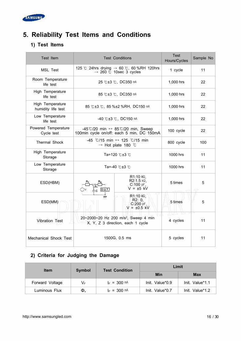
5. Reliability Test Items and Conditions1) Test Items
Test Item Test Conditions TestHours/Cycles
Sample No
MSL Test 125℃ 24hrs drying → 60℃, 60 %RH 120hrs→ 260℃ 10sec 3 cycles 1 cycle 11
Room Temperaturelife test 25℃±3℃, DC350㎃ 1,000 hrs 22
High Temperaturelife test 85℃±3℃, DC350㎃ 1,000 hrs 22
High Temperaturehumidity life test 85℃±3℃, 85 %±2 %RH, DC150㎃ 1,000 hrs 22
Low Temperaturelife test -40℃±3℃, DC150㎃ 1,000 hrs 22
Powered TemperatureCycle test
-45℃/20 min ↔ 85℃/20 min, Sweep100min cycle on/off: each 5 min, DC 150mA 100 cycle 22
Thermal Shock -45 ℃/15 min ↔ 125 ℃/15 min→ Hot plate 180 ℃
800 cycle 100
High TemperatureStorage Ta=120℃±3℃ 1000 hrs 11
Low TemperatureStorage Ta=-40℃±3℃ 1000 hrs 11
ESD(HBM)R1:10㏁,R2:1.5㏀,C:100㎊,V = ±5 kV
5 times 5
ESD(MM)R1:10㏁,R2: 0,C:200㎊,
V = ±0.5 kV5 times 5
Vibration Test20~2000~20 Hz 200 m/s2, Sweep 4 min
X, Y, Z 3 direction, each 1 cycle 4 cycles 11
Mechanical Shock Test 1500G, 0.5 ms 5 cycles 11
2) Criteria for Judging the Damage
Item Symbol Test ConditionLimit
Min Max
Forward Voltage VF IF = 300㎃ Init. Value*0.9 Init. Value*1.1
Luminous Flux Φv IF = 300㎃ Init. Value*0.7 Init. Value*1.2
http://www.samsungled.com 17 / 30
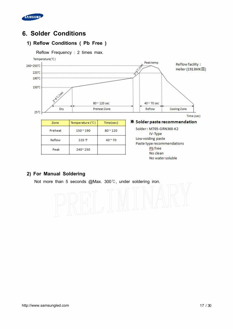
6. Solder Conditions1) Reflow Conditions ( Pb Free )
Reflow Frequency : 2 times max.
2) For Manual SolderingNot more than 5 seconds @Max. 300℃, under soldering iron.
http://www.samsungled.com 18 / 30
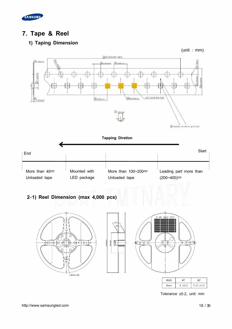
7. Tape & Reel1) Taping Dimension
(unit : mm)
2-1) Reel Dimension (max 4,000 pcs)
Tolerance ±0.2, unit: mm
More than 40㎜Unloaded tape
Mounted withLED package
Leading part more than(200~400)㎜
More than 100~200㎜Unloaded tape
End Start
Tapping Diretion
http://www.samsungled.com 19 / 30
(1) Quantity : The quantity/Reel to be 4,000 pcs.(2) Cumulative Tolerance : Cumulative tolerance/10 pitches to be ±0.2mm(3) Packaging : P/N, Manufacturing data code no. and quantity to be indicated on a
damp proof Package.
http://www.samsungled.com 20 / 30
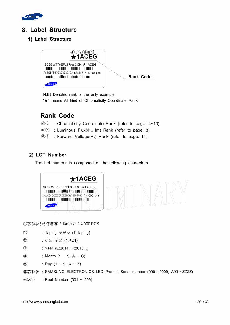
8. Label Structure1) Label Structure
N.B) Denoted rank is the only example.'★' means All kind of Chromaticity Coordinate Rank.
Rank Codeⓐⓑ : Chromaticity Coordinate Rank (refer to page. 4~10)ⓒⓓ : Luminous Flux(Φv, lm) Rank (refer to page. 3)ⓔⓕ : Forward Voltage(VF) Rank (refer to page. 11)
2) LOT NumberThe Lot number is composed of the following characters
①②③④⑤⑥⑦⑧⑨ / Iⓐⓑⓒ / 4,000 PCS
① : Taping 구분자 (T:Taping)
② : 라인 구분 (1:KC1)
③ : Year (E:2014, F:2015...)
④ : Month (1 ~ 9, A ~ C)
⑤ : Day (1 ~ 9, A ~ Z)
⑥⑦⑧⑨ : SAMSUNG ELECTRONICS LED Product Serial number (0001~0009, A001~ZZZZ)
ⓐⓑⓒ : Reel Number (001 ~ 999)
SCS8WT78EFL1★08CCK ★1ACEGIIIIIIIIIIIIIIIIIIIIIIIIIIIIIIIIIIIIIIIIIIIIIIIII
①②③④⑤⑥⑦⑧⑧⑨/ Iⓐⓑⓒ / 4,000 pcsIIIIIIIIIIIIIIIIIIIIIIIIIIIIIIIIIIIIIIIIII
ⓐⓑⓒⓓⓔⓕ
Rank Code
★1ACEG
SCS8WT78EFL1★08CCK ★1ACEGIIIIIIIIIIIIIIIIIIIIIIIIIIIIIIIIIIIIIIIIIIIIIIIII
①②③④⑤⑥⑦⑧⑧⑨/ Iⓐⓑⓒ / 4,000 pcsIIIIIIIIIIIIIIIIIIIIIIIIIIIIIIIIIIIIIIIIII
★1ACEG
http://www.samsungled.com 21 / 30
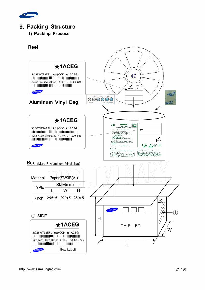
9. Packing Structure1) Packing Process
Reel
Box (Max. 7 Aluminum Vinyl Bag)
Aluminum Vinyl Bag
LEVEL
2a
LEVEL
2a
① SIDE
Material : Paper(SW3B(A))
TYPESIZE(mm)
L W H
7inch 295±5 290±5 260±5
CHIP LED
①H
W
L
SCS8WT78EFL1★08CCK ★1ACEGIIIIIIIIIIIIIIIIIIIIIIIIIIIIIIIIIIIIIIIIIIIIIIIII
①②③④⑤⑥⑦⑧⑧⑨/ Iⓐⓑⓒ / 4,000 pcsIIIIIIIIIIIIIIIIIIIIIIIIIIIIIIIIIIIIIIIIII
★1ACEG
SCS8WT78EFL1★08CCK ★1ACEGIIIIIIIIIIIIIIIIIIIIIIIIIIIIIIIIIIIIIIIIIIIIIIIII
①②③④⑤⑥⑦⑧⑧⑨/ Iⓐⓑⓒ / 4,000 pcsIIIIIIIIIIIIIIIIIIIIIIIIIIIIIIIIIIIIIIIIII
★1ACEG
SCS8WT78EFL1★08CCK ★1ACEGIIIIIIIIIIIIIIIIIIIIIIIIIIIIIIIIIIIIIIIIIIIIIIIII
①②③④⑤⑥⑦⑧⑧⑨/ Iⓐⓑⓒ / 28,000 pcsIIIIIIIIIIIIIIIIIIIIIIIIIIIIIIIIIIIIIIIIII
★1ACEG
[Box Label]
http://www.samsungled.com 22 / 30
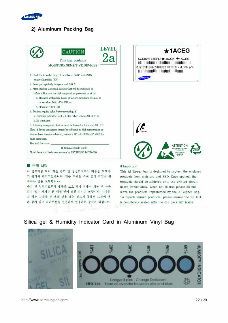
2) Aluminum Packing Bag
Silica gel & Humidity Indicator Card in Aluminum Vinyl Bag
SCS8WT78EFL1★08CCK ★1ACEGIIIIIIIIIIIIIIIIIIIIIIIIIIIIIIIIIIIIIIIIIIIIIIIII
①②③④⑤⑥⑦⑧⑧⑨/ Iⓐⓑⓒ / 4,000 pcsIIIIIIIIIIIIIIIIIIIIIIIIIIIIIIIIIIIIIIIIII
★1ACEG
http://www.samsungled.com 23 / 30
10. Precaution for use1) For over-current-proof function, customers are recommended to apply resistors to
prevent sudden change of the current caused by slight shift of the voltage.과전류 방지를 위해 전압의 미세한 이동에 의해 야기되는 전류의 순간 변화를 방지하기
위해 저항 등의 설치를 권장함.
2) This device should not be used in any type of fluid such as water, oil, organicsolvent, etc. When washing is required, IPA is recommended to use.제품은 물, 오일, 유기물과 같은 액체 타입에서의 사용은 제한되며,세정이 필요할 시에는 IPA 사용을 권장함.
3) When the LEDs illuminate, operating current should be decided after considering theambient maximum temperature.LED의 발광 시, 동작 전류는 주변 최고온도를 고려하여 결정되어야 함.
4) LEDs must be stored in a clean environment.If the LEDs are to be stored for 3 months or more after being shipped fromSamsung Electronics, they should be packed by a sealed container with nitrogen gasinjected.(Shelf life of sealed bags: 12 months, temp. ~40℃, ~90%RH)LED의 보관은 청정한 환경에서 보존되어져야 하며, 만약 삼성전자로부터 공급받는 후
3개월 또는 그 이상 보관이 필요하다면 질소 가스를 동봉한 보존용기에 보관되어야 함.(보존 bag의 수명 : 12 개월, 보존 온도 ~40℃, 습도 ~90%RH)
5) After storage bag is open, device subjected to soldering, solder reflow, or otherhigh temperature processes must be:보존 Bag이 개봉된 후에, 납땜이나 reflow등의 높은 온도에 노출되는 제품은 다음의
사항에 부합되어야 함.
a. Mounted within 672 hours(28 days) at an assembly line with a condition of nomore than 30℃/60%RH,
a. 제품은 30℃/60%RH보다 같거나 낮은 조립조건에서 672시간(28일)이내에 조립해야 함.b. Stored at <10%RH.b. 10% 이하의 상대습도에서 보관되어야 함.
6) Repack unused Products with anti-moisture packing, fold to close any opening andthen store in a dry place.사용하지 않은 제품은 방습팩에 넣어 개봉 부위를 닫아서 다시 포장한 후,건조한 장소에서 보관할 것을 권장함.
http://www.samsungled.com 24 / 30
7) Devices require baking before mounting, if humidity card reading is >60% at 23±5℃.만약 습도표시카드의 수치가 23±5℃에서 60% 이상이라면, 제품 실장 전 baking해야 함.
8) Devices must be baked for 1 hour at 60±5℃, if baking is required.만약 baking이 필요하다면, 제품은 60±5℃에서 1시간 정도 baking 되어야 함.
9) The LEDs are sensitive to the static electricity and surge. It is recommended touse a wrist band or anti-electrostatic glove when handling the LEDs.LED는 정전기 및 서지에 민감한 제품이므로, LED 제품을 다룰 시에는 정전기
방지장갑이나 손목밴드를 사용하기를 권장함.
If voltage exceeding the absolute maximum rating is applied to LEDs, it may causedamage or even destruction to LED devices.만약 절대 허용치를 초과하는 전압이 LED에 가해지면, LED 소자는 파괴되거나
손상될 수 있음.
Damaged LEDs may show some unusual characteristics such as increase in leakcurrent, lowered turn-on voltage, or abnormal lighting of LEDs at low current.손상된 제품은 누설전류의 증가, Turn on 전압의 저하, 저 전류에서의 점등불량 등의
이상 거동을 보일 수 있음.
10) VOCs (volatile organic compounds) can be generated from adhesives, flux, hardeneror organic additives used in luminaires (fixtures).Transparent LED silicone encapsulant is permeable to those chemicals andthey may lead a discoloration of encapsualnt when they expose to heat or light.
VOCs(휘발성 유기 화합물)는 등기구에 사용되는 접착제, Flux, 경화제,유기물 첨가제에서 발생하여 LED 실리콘 봉지제를 투과하고,빛 또는 열에 노출되었을 때 변색이 발생 할 수 있음.
This phenomenon can cause a significant loss of light emitted(output) from theluminaires(fixtures).이러한 현상은 등기구로부터 나오는 빛의 중대한 손실을 줄 수 있음.
In order to prevent these problems, we recommend you to know the physicalproperties of the materials used in luminaires, They must be selected carefully.
이러한 문제 발생 방지를 위해서, 등기구에 사용되는 자재에 대한 물성을 알고
주의하여 선택 되어야함.
http://www.samsungled.com 25 / 30
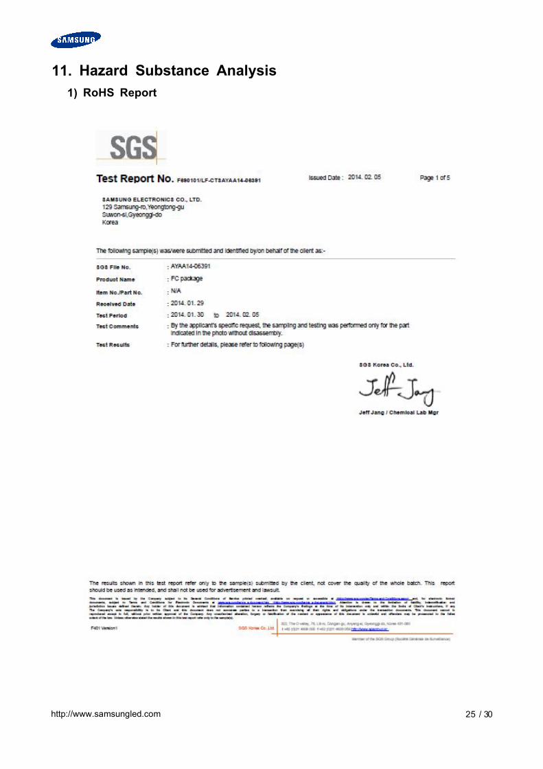
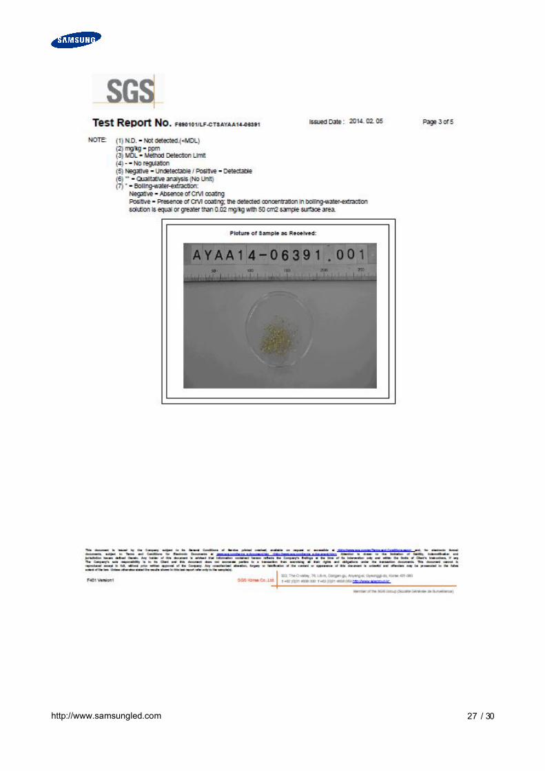
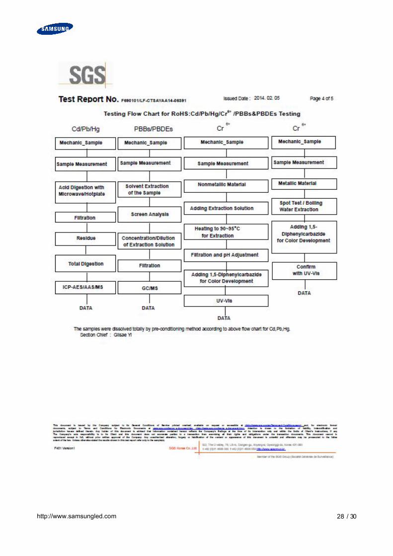
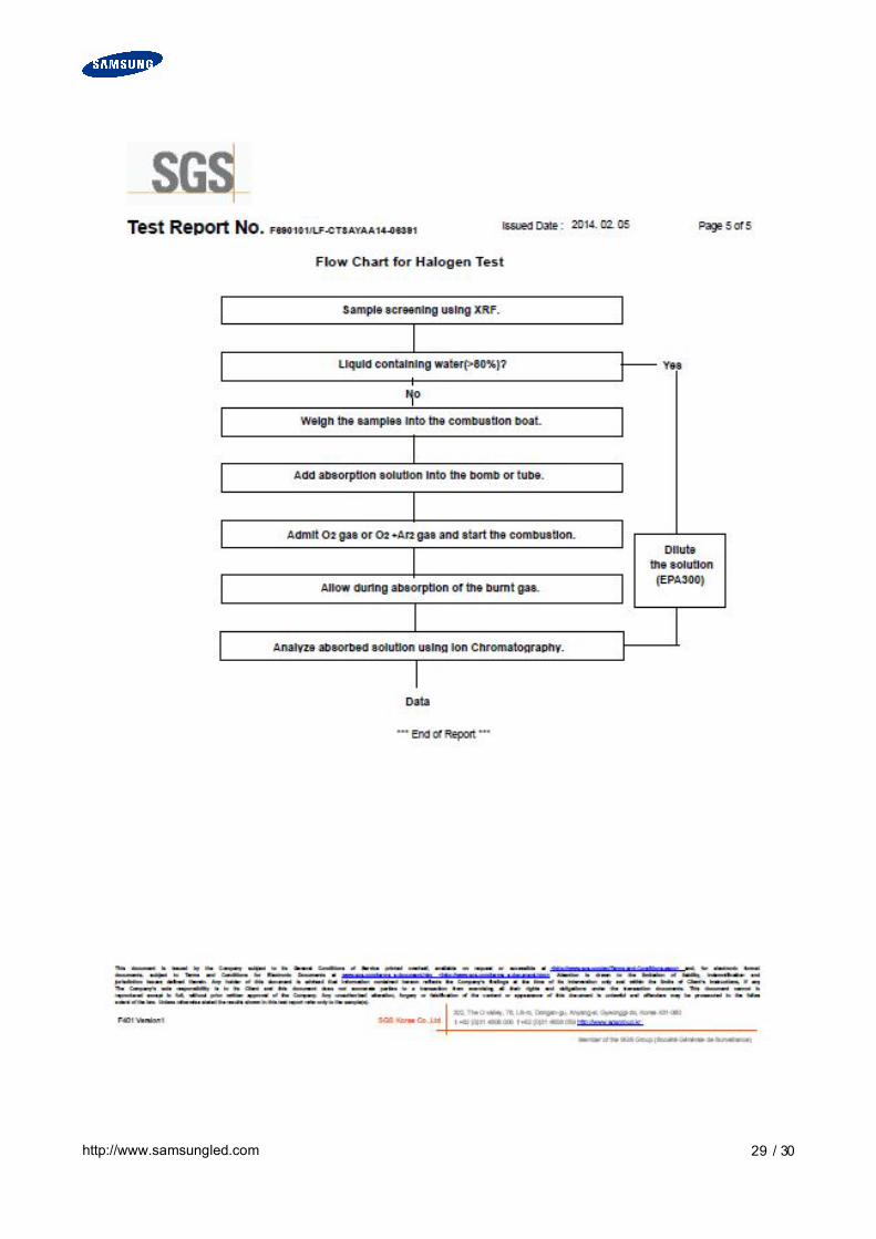
11. Hazard Substance Analysis1) RoHS Report
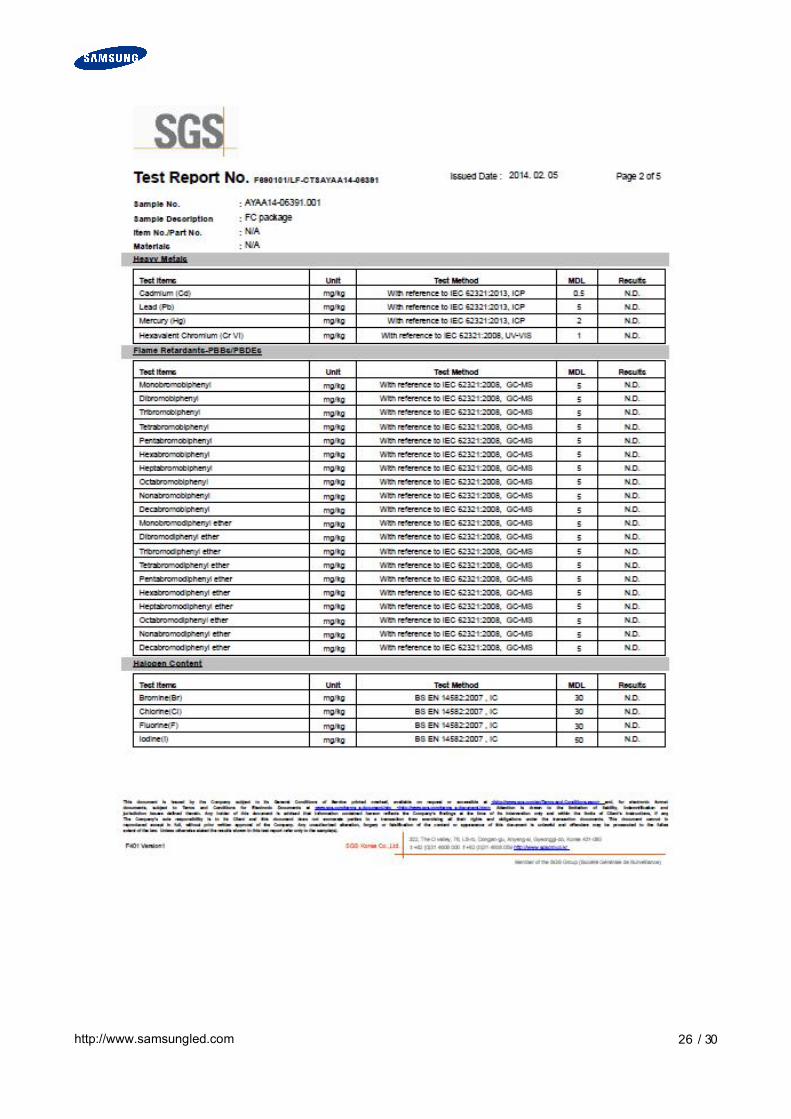
http://www.samsungled.com 26 / 30
http://www.samsungled.com 27 / 30
http://www.samsungled.com 28 / 30
http://www.samsungled.com 29 / 30
http://www.samsungled.com 30 / 30
Revision History
Date Revision HistoryWriter
Drawn Approved2014.03.24 New version J.H.Kim Hakhwan Kim