Embed Size (px)
Citation preview
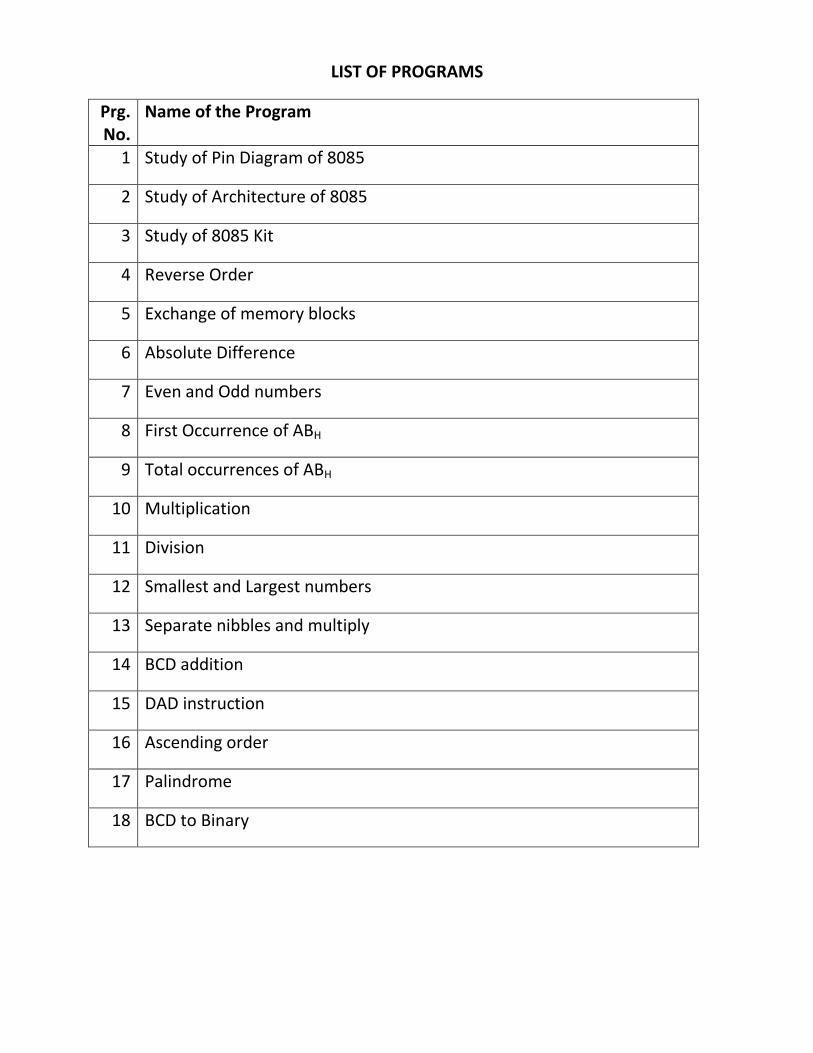
LIST OF PROGRAMS
Prg. No.
Name of the Program
1 Study of Pin Diagram of 8085
2 Study of Architecture of 8085
3 Study of 8085 Kit
4 Reverse Order
5 Exchange of memory blocks
6 Absolute Difference
7 Even and Odd numbers
8 First Occurrence of ABH
9 Total occurrences of ABH
10 Multiplication
11 Division
12 Smallest and Largest numbers
13 Separate nibbles and multiply
14 BCD addition
15 DAD instruction
16 Ascending order
17 Palindrome
18 BCD to Binary
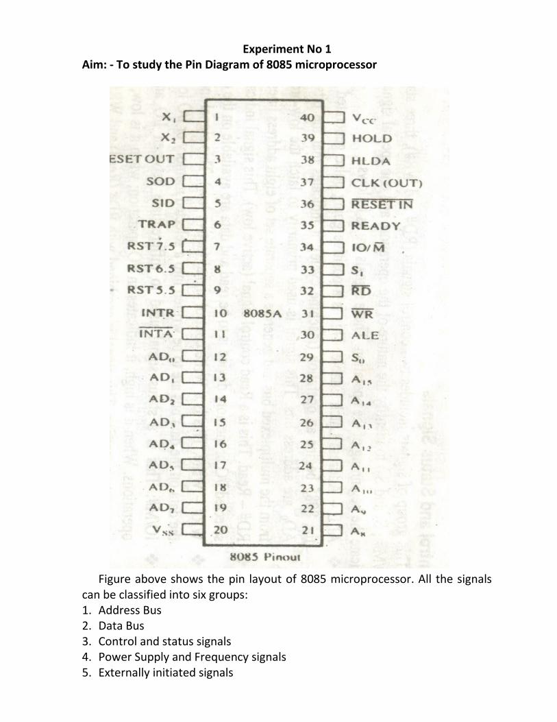
Experiment No 1 Aim: - To study the Pin Diagram of 8085 microprocessor
Figure above shows the pin layout of 8085 microprocessor. All the signals can be classified into six groups: 1. Address Bus 2. Data Bus 3. Control and status signals 4. Power Supply and Frequency signals 5. Externally initiated signals
6. Serial I/O ports Address Bus
8085 has eight lines, 158 AA , which are unidirectional and used as the
higher order address bus. Multiplexed Address/Data Bus
The signal lines 07 ADAD are bidirectional; they serve a dual purpose. They
are used as the low-order address bus as well as the data bus. In executing an instruction, during the earlier part pf the cycle, these lines are used as the low-order address bus. During the later part of the cycle, these lines are used as the data bus. For separating the low-order address bus and data bus, a separate address latch called ALE is used. Control and Status Signals:
This group of signals includes two control signals ( DR and RW ), three status
signals ( MIO / , 1S and 0S ) to identify the nature of the operation, and one special
signal (ALE) to indicate the beginning of the operation. These signals are as follows:
ALE – Address Latch Enable. This is a positive going pulse generated every time the 8085 begins an operation (machine cycle); it indicates that the bits 7AD - 0AD are address bits. This signal is used primarily to latch the low-
order address from the multiplexed bus and generate a separate set of eight address lines, 07 AA .
DR - Read. This is a Read control signal (active low). This signal indicates
that the selected I/O or memory device is to be read and data are available on the data bus.
RW - Write. This is a Write control signal (active low). This signal indicates
that the data on the data bus are to be written into a selected memory or I/O location.
IO/ M . This is a status signal used to differentiate between I/O and memory operations. When it is high, it indicates an I/O operation; when it
is low, it indicates a memory operation. This signal is combined with DR
(Read) and RW (Write) to generate I/O memory control signals.
1S and 0S : These status signals,similar to IO/ M , can identify various
operations, but they are rarely used in small systems. Power Supply and Clock Frequency The power supply and grequency signals are as follows: CCV +5V power supply.
SSV Ground Reference.
21, XX A crystal (or RC, LC network) is connected at these two pins. The
frequency is internally divided by two; therefore, to operate a system at 3 MHz, the crystal should have a frequency of 6 MHz.
CLK (OUT) – Clock Output: This signal can be used as the system clock for other devices.
Externally initiated signals including interrupts: The 8085 has five interrupt signals that can be used to interrupt a program
execution. The microprocessor acknowledges an interrupt request by the INTA
(Interrupt Acknowledge) signal. The externally generated signals in 8085 are as follows:
Name of the Interrupt
Description
INTR(Input) Interrupt Request: This is used as a general purpose interrupt.
INTA(Output) Interrupt Acknowledgement: This is used to acknowledge an interrupt.
RST 7.5, RST 6.5 and RST 5.5 (Inputs)
Restart Interrupt: These are vectored interrupts and transfer the program control to the INTR interrupt. The priority order is 7.5, 6.5 and 5.5.
TRAP (Input) This is a non-maskable interrupt and has the highest priority. HOLD (Input) This signal indicates that a peripheral such as a DMA (Direct
Memory Access) controller is requesting the use of the address bus and data bus.
HLDA(Output) Hold Acknowledge: This signal acknowledges the HOLD request. READY(Input) This signal is used to delay the microprocessor Read or Write
cycles until a slow-responding peripheral is ready to send or accept data. When this signal goes low, the microprocessor waits for an integral number of clock cycles until it goes high.
RESETIN (Input) When the signal on this pin goes low, the program counter is set to zero, the buses are tri-stated, and the MPU is reset.
RESET OUT(Output) This signal indicates that the MPU is being reset. The signal can be used to reset other devices.
Serial I/O Ports The 8085 has two signals to implement the serial transmissions: SID(Serial Input Data) and SOD (Serial Output Data). Conclusion: - Thus we have studied the Pin Diagram of 8085.
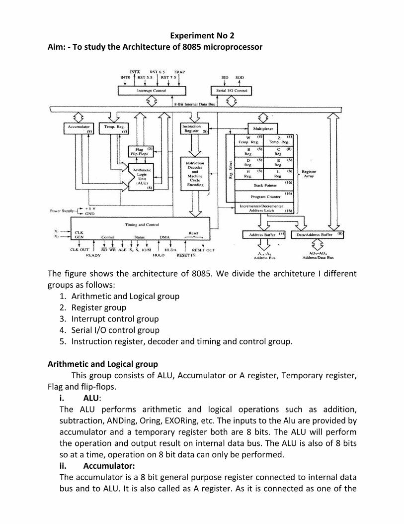
Experiment No 2 Aim: - To study the Architecture of 8085 microprocessor
The figure shows the architecture of 8085. We divide the architeture I different groups as follows:
1. Arithmetic and Logical group 2. Register group 3. Interrupt control group 4. Serial I/O control group 5. Instruction register, decoder and timing and control group.
Arithmetic and Logical group This group consists of ALU, Accumulator or A register, Temporary register, Flag and flip-flops.
i. ALU: The ALU performs arithmetic and logical operations such as addition, subtraction, ANDing, Oring, EXORing, etc. The inputs to the Alu are provided by accumulator and a temporary register both are 8 bits. The ALU will perform the operation and output result on internal data bus. The ALU is also of 8 bits so at a time, operation on 8 bit data can only be performed. ii. Accumulator: The accumulator is a 8 bit general purpose register connected to internal data bus and to ALU. It is also called as A register. As it is connected as one of the
inputs to ALU, it is used in most of the arithmetic and logic instructions. After performing an operation the Alu places its result on internal data bus, from there it is generally stored in accumulator. So accumulator is an integral part in performing different operations along with ALU. Also accumulator is used during I/O operations. iii. Temporary register: The other input to ALU is given by temporary register. This register is not available for user, it is only used internally by the microprocessor, so the name given temporary register. To perform arithmetic and logical operations microprocessor assumes one data available in accumulator and takes another data from other register (depends on instruction) into temporary register and then performs operation on the two data operands. Example: ADD B instruction adds A reg + B reg. The result is stored in register A. in this case one data is available in A reg, and other data from B register is transferred to temporary register and then add operation is performed on them. This temporary register is also used for other operation also, such as register to register data transfer, etc. iv. Flag: The flag is nothing but a group of flip flops used to give status of different operations result. As flag register is connected to ALU, when an operation is performed by ALU the status of result will be stored in flip-flops. It is clear that for all other operations the flag doesn’t get affected, it will only give status if a operation is performed in ALU. The position of various flags available in 8085 as shown below:
7D 6D 5D 4D 3D
2D 1D 0D
S Z X AC X P X CY
1. CY- Carry Flag: - If an operation peformed in ALU generates a carry from 7D
to next stage, the CY flag is set. It works as 9th bit for addition and as borrow flag for subtraction. If there is no carry out of MSB bit ie 7D of result
the CY flag is reset. 2. AC – Auxiliary Carry Flag: If an operation performed by ALU generates a
carry from lower nibble i.e. 0D - 3D , to upper/higher nibble i.e. 4D - 7D
internally by microprocessor, the AC flag is set. i.e. carry given by 3D to 4D .
This is not general flag. It is only used internally by microprocessor to perform binary to BCD conversion. It is not available for programmer for changing the sequence as it is for other 4 flags.
3. Z – Zero Flag: - If an operation results in zero as a result the zero flag is set. If the result is not zero the zero flag is reset.
4. S – Sign Flag: - In sign magnitudeformat always sign of a number is indicated by 7D bit. This bit is exact replica of 7D bit of result. If 7D =1, the
flag is set and if 7D =0, the flag is reset.
5. P – Parity Flag: - This bit is used to indicate the perity of the result. if the result contain even number of 1’s this flag is set. If the result contains odd number of 1’s this flag is reset.
Register Group: This group consists of 3 types of registers.
i. Temporary registers ii. General purpose registers iii. Special purpose registers
i. Temporary registers (W and Z) These are not avavilable for user and used only for internal operations such as to store operand immediate operand or address of memory. These are used internally by the microprocessor for execution of certain instructions. ii. General purpose registers: The 8085 contains 6 general purpose registers of 8 bits each, named as B, C, D, E, H and L. these can be used to store 8 bits of data or can be used to form a register pair to store 16 bit data. The register pairs available are BC, DE and HL. These registers are programmable by user. User can store any data in these registers and use it to perform different operations. iii. Special purpose registers: The 8085 contains 3 special purpose registers such as program counter, increment/decrement latch and stack pointer. a. Program counter:
This is a 16 bit register used for execution of program. This register always points to address of memory from where the next instruction is to be fetched and executed. When microprocessor performs one operation of taking instruction i.e. fetching, the PC contents are automatically incremented by one to point to next location. In this way PC keeps the track for execution of program. Upon reset PC contents are set to 0000H, so after reset operation microprocessor will start execution of program from 0000H onwards.
b. Stack Pointer: This is a 16 bit register used to define the stack starting address. Stack is a reserved portion of memory where temporary information may be stored or taken back under software control. The stack pointer is used to keep track of data stored.
c. Increment/Decrement latch:
This 16 bit register is used in cordination with PC and SP, to increment or decrement the contents of PC and SP registers.
In coordination with these registers two buffers are used.
a. Address buffer: This is an 8 bit uni-directional buffer used for 8A to 15A address lines. These
are used to output higher order address on 8A to 15A . When they are not in
use or under certain conditions such as reset, hold, halt these are used to tristate 8A to 15A address lines.
b. Address/Data buffer: This is an 8 bit bidirectional buffer used for address and data. These 2 signals are multiplexed on 0AD to 7AD lines. In earlier part it is used to
output lower order address 0A to 7A and in later part it is used to input or
output data 0D to 7D . These addresses are taken from address lines and
data is taken or transferred on internal data bus. Under certain conditions such as reset, hold, halt these are used to tristate 0A to 7A address/data
lines. The various sources of addresses for the address register includes program counter, stack pointer, temporary registers, BC pair, DE pair and HL pair.
Interrupt Control This block accepts different interrupt request input such as TRAP, RST 7.5, RST 6.5, RST 5.5 and INTR, and informs control logic to take action in response to each signal. The response for TRAP, RST 7.5, RST 6.5, RST 5.5 is CALL at restart address.
But for INTR, it generates a INTAsignal and expects external device should insert a RST code or CALL instructions. Serial I/O Control Group The data transferred on 0D to 7D lines is a parallel data, but under certain
condition is advantageous to use serial data transfer. 8085 implements this using SID and SOD signal and the data on these lines is accepted or transferred under software control by serial I/O control block. Instruction Register, Decoder and Control Group
i. Instruction register: When an instruction is fetched from memory it is loaded in instruction
register from there it is provided to decoder for decoding. This register is only activated when instruction code or opcode is available on internal data bus. It is non programmable register i.e. not available for programmer use. It accepts
only opcode of instruction, operands are not accepted by this instead they are stored in registers. ii. Instruction decoder:
This accepts a bit pattern from Instruction register, decodes it and gives the different information to control logic. The information includes what operation is to be performed, who is going to perform it, how many operand bytes the instruction contains, etc. iii. Timing and Control Unit: This is a control section of 8085. This accepts information from instruction decoder and generates micro steps to perform it so 8085 is called as microprogrammed. In addition to this the block accepts clock inputs and performs sequencing and synchronising operations required for communication between microprocessor and peripheral devices. To implement this it used different status and control signals. For internal operations depending on decoder signals the steps or sequence is generally prepared. As an example we take the transfer of data from B register to A register. To implement this, steps taken by 8085 are: i. Take data from b register on to internal data bus. ii. Enable temporary register of ALU group to accept data from internal
data bus. iii. Again enable the temporary register to send the data on internal data
bus. iv. Enable A register to accept data from internal data bus. In this way, the steps are implemented for execution of instructions in 8085.
Conclusion: - Thus we have studied Architecture of 8085.
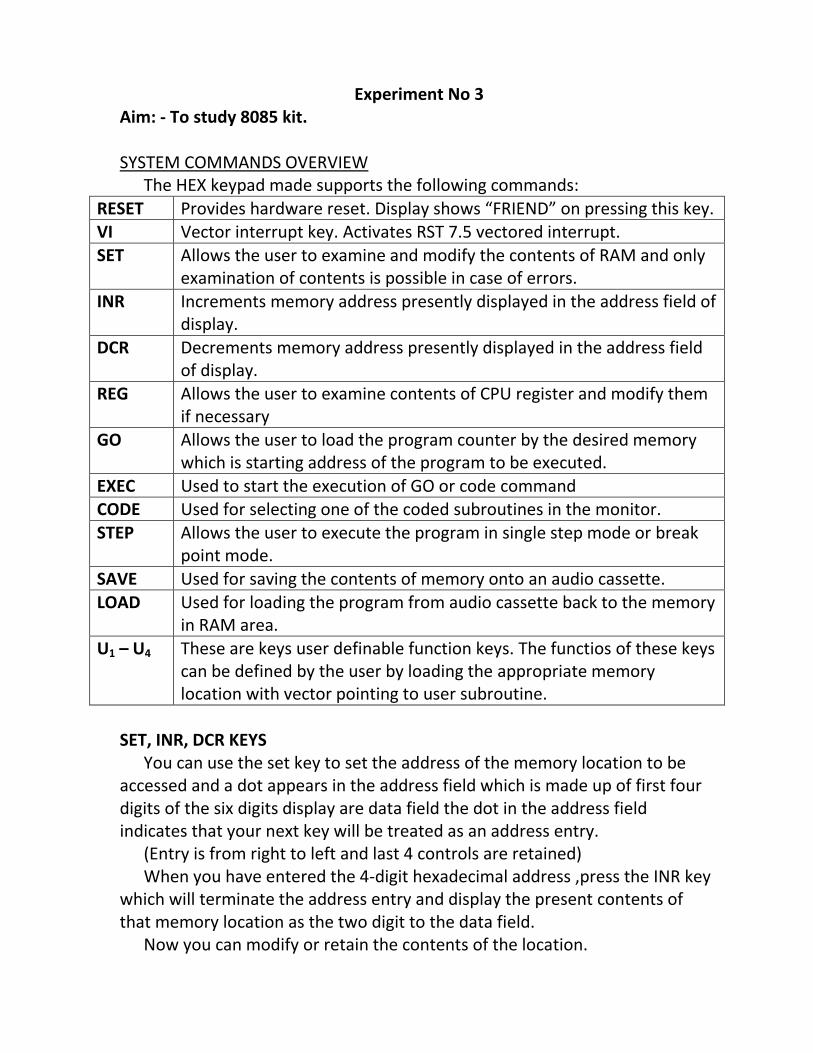
Experiment No 3
Aim: - To study 8085 kit. SYSTEM COMMANDS OVERVIEW The HEX keypad made supports the following commands:
RESET Provides hardware reset. Display shows “FRIEND” on pressing this key. VI Vector interrupt key. Activates RST 7.5 vectored interrupt.
SET Allows the user to examine and modify the contents of RAM and only examination of contents is possible in case of errors.
INR Increments memory address presently displayed in the address field of display.
DCR Decrements memory address presently displayed in the address field of display.
REG Allows the user to examine contents of CPU register and modify them if necessary
GO Allows the user to load the program counter by the desired memory which is starting address of the program to be executed.
EXEC Used to start the execution of GO or code command CODE Used for selecting one of the coded subroutines in the monitor.
STEP Allows the user to execute the program in single step mode or break point mode.
SAVE Used for saving the contents of memory onto an audio cassette.
LOAD Used for loading the program from audio cassette back to the memory in RAM area.
U1 – U4 These are keys user definable function keys. The functios of these keys can be defined by the user by loading the appropriate memory location with vector pointing to user subroutine.
SET, INR, DCR KEYS You can use the set key to set the address of the memory location to be accessed and a dot appears in the address field which is made up of first four digits of the six digits display are data field the dot in the address field indicates that your next key will be treated as an address entry. (Entry is from right to left and last 4 controls are retained) When you have entered the 4-digit hexadecimal address ,press the INR key which will terminate the address entry and display the present contents of that memory location as the two digit to the data field. Now you can modify or retain the contents of the location.
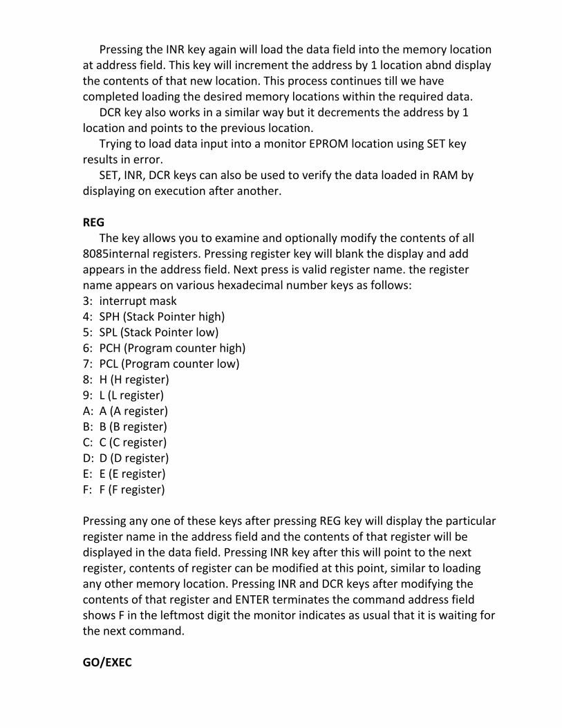
Pressing the INR key again will load the data field into the memory location at address field. This key will increment the address by 1 location abnd display the contents of that new location. This process continues till we have completed loading the desired memory locations within the required data. DCR key also works in a similar way but it decrements the address by 1 location and points to the previous location. Trying to load data input into a monitor EPROM location using SET key results in error. SET, INR, DCR keys can also be used to verify the data loaded in RAM by displaying on execution after another. REG The key allows you to examine and optionally modify the contents of all 8085internal registers. Pressing register key will blank the display and add appears in the address field. Next press is valid register name. the register name appears on various hexadecimal number keys as follows: 3: interrupt mask 4: SPH (Stack Pointer high) 5: SPL (Stack Pointer low) 6: PCH (Program counter high) 7: PCL (Program counter low) 8: H (H register) 9: L (L register) A: A (A register) B: B (B register) C: C (C register) D: D (D register) E: E (E register) F: F (F register) Pressing any one of these keys after pressing REG key will display the particular register name in the address field and the contents of that register will be displayed in the data field. Pressing INR key after this will point to the next register, contents of register can be modified at this point, similar to loading any other memory location. Pressing INR and DCR keys after modifying the contents of that register and ENTER terminates the command address field shows F in the leftmost digit the monitor indicates as usual that it is waiting for the next command. GO/EXEC
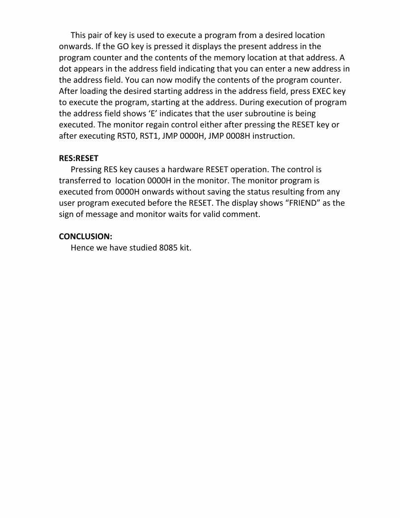
This pair of key is used to execute a program from a desired location onwards. If the GO key is pressed it displays the present address in the program counter and the contents of the memory location at that address. A dot appears in the address field indicating that you can enter a new address in the address field. You can now modify the contents of the program counter. After loading the desired starting address in the address field, press EXEC key to execute the program, starting at the address. During execution of program the address field shows ‘E’ indicates that the user subroutine is being executed. The monitor regain control either after pressing the RESET key or after executing RST0, RST1, JMP 0000H, JMP 0008H instruction. RES:RESET Pressing RES key causes a hardware RESET operation. The control is transferred to location 0000H in the monitor. The monitor program is executed from 0000H onwards without saving the status resulting from any user program executed before the RESET. The display shows “FRIEND” as the sign of message and monitor waits for valid comment. CONCLUSION: Hence we have studied 8085 kit.
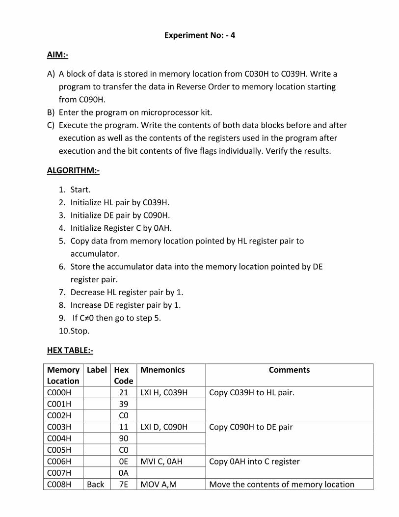
Experiment No: - 4
AIM:-
A) A block of data is stored in memory location from C030H to C039H. Write a
program to transfer the data in Reverse Order to memory location starting
from C090H.
B) Enter the program on microprocessor kit.
C) Execute the program. Write the contents of both data blocks before and after
execution as well as the contents of the registers used in the program after
execution and the bit contents of five flags individually. Verify the results.
ALGORITHM:-
1. Start.
2. Initialize HL pair by C039H.
3. Initialize DE pair by C090H.
4. Initialize Register C by 0AH.
5. Copy data from memory location pointed by HL register pair to
accumulator.
6. Store the accumulator data into the memory location pointed by DE
register pair.
7. Decrease HL register pair by 1.
8. Increase DE register pair by 1.
9. If C≠0 then go to step 5.
10. Stop.
HEX TABLE:-
Memory Location
Label Hex Code
Mnemonics Comments
C000H 21 LXI H, C039H Copy C039H to HL pair.
C001H 39 C002H C0
C003H 11 LXI D, C090H Copy C090H to DE pair C004H 90
C005H C0
C006H 0E MVI C, 0AH Copy 0AH into C register C007H 0A
C008H Back 7E MOV A,M Move the contents of memory location
Pointed by HL pair to accumulator.
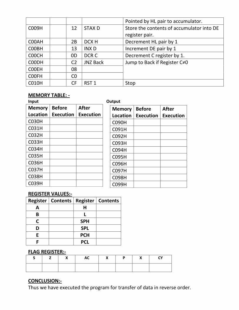
C009H 12 STAX D Store the contents of accumulator into DE register pair.
C00AH 2B DCX H Decrement HL pair by 1 C00BH 13 INX D Increment DE pair by 1
C00CH 0D DCR C Decrement C register by 1. C00DH C2 JNZ Back Jump to Back if Register C≠0
C00EH 08
C00FH C0 C010H CF RST 1 Stop
MEMORY TABLE: - Input Output
REGISTER VALUES:- Register Contents Register Contents
A H B L
C SPH
D SPL E PCH
F PCL
FLAG REGISTER:- S Z X AC X P X CY
CONCLUSION:- Thus we have executed the program for transfer of data in reverse order.
Memory Location
Before Execution
After Execution
C030H C031H
C032H C033H
C034H
C035H C036H
C037H C038H
C039H
Memory Location
Before Execution
After Execution
C090H
C091H C092H
C093H C094H
C095H C096H
C097H
C098H C099H
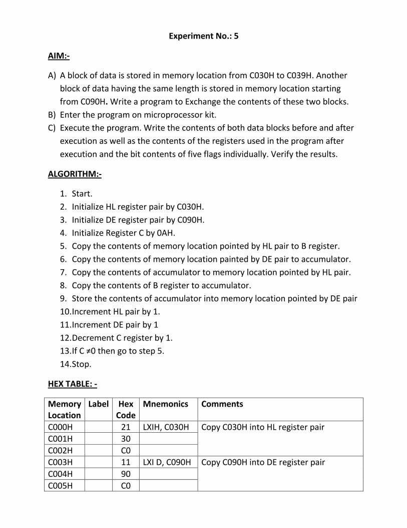
Experiment No.: 5
AIM:-
A) A block of data is stored in memory location from C030H to C039H. Another
block of data having the same length is stored in memory location starting
from C090H. Write a program to Exchange the contents of these two blocks.
B) Enter the program on microprocessor kit.
C) Execute the program. Write the contents of both data blocks before and after
execution as well as the contents of the registers used in the program after
execution and the bit contents of five flags individually. Verify the results.
ALGORITHM:-
1. Start.
2. Initialize HL register pair by C030H.
3. Initialize DE register pair by C090H.
4. Initialize Register C by 0AH.
5. Copy the contents of memory location pointed by HL pair to B register.
6. Copy the contents of memory location painted by DE pair to accumulator.
7. Copy the contents of accumulator to memory location pointed by HL pair.
8. Copy the contents of B register to accumulator.
9. Store the contents of accumulator into memory location pointed by DE pair
10. Increment HL pair by 1.
11. Increment DE pair by 1
12. Decrement C register by 1.
13. If C ≠0 then go to step 5.
14. Stop.
HEX TABLE: -
Memory Location
Label Hex Code
Mnemonics Comments
C000H 21 LXIH, C030H Copy C030H into HL register pair C001H 30
C002H C0 C003H 11 LXI D, C090H Copy C090H into DE register pair
C004H 90
C005H C0
C006H 0E MVI C, 0AH Copy 0AH into C register
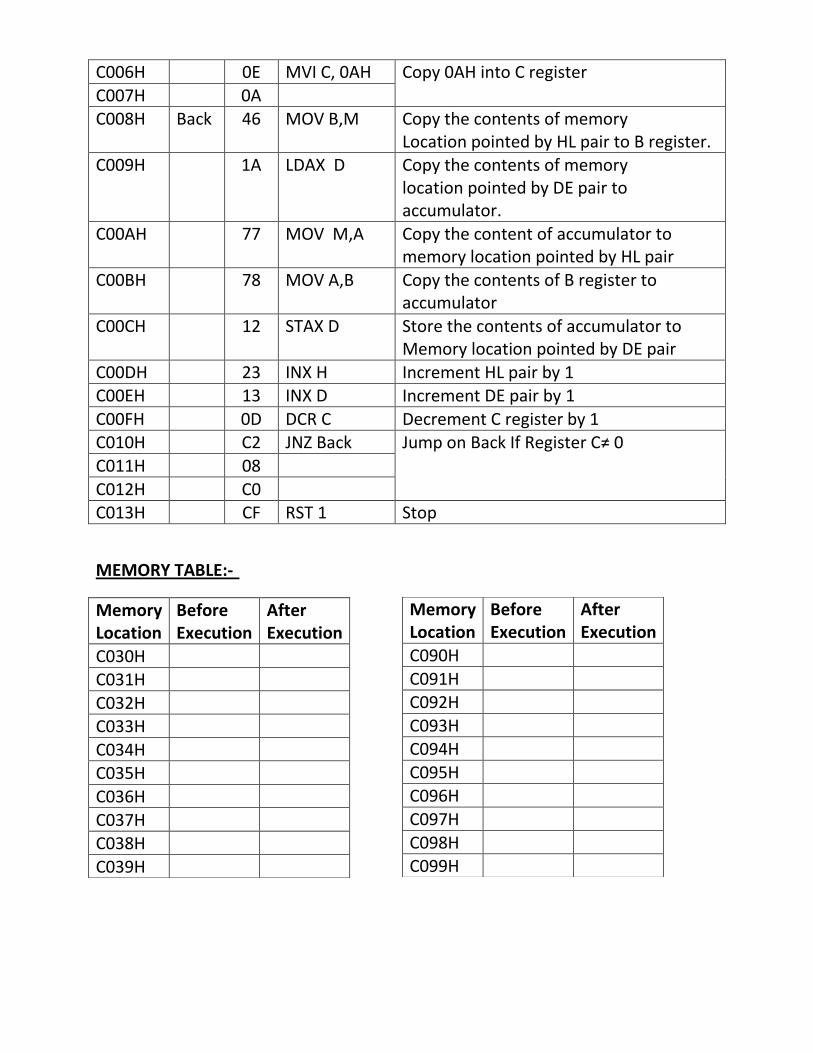
C007H 0A C008H Back 46 MOV B,M Copy the contents of memory
Location pointed by HL pair to B register. C009H 1A LDAX D Copy the contents of memory
location pointed by DE pair to accumulator.
C00AH 77 MOV M,A Copy the content of accumulator to memory location pointed by HL pair
C00BH 78 MOV A,B Copy the contents of B register to accumulator
C00CH 12 STAX D Store the contents of accumulator to Memory location pointed by DE pair
C00DH 23 INX H Increment HL pair by 1 C00EH 13 INX D Increment DE pair by 1
C00FH 0D DCR C Decrement C register by 1 C010H C2 JNZ Back Jump on Back If Register C≠ 0
C011H 08
C012H C0 C013H CF RST 1 Stop
MEMORY TABLE:-
Memory Location
Before Execution
After Execution
C030H C031H
C032H C033H
C034H C035H
C036H
C037H C038H
C039H
Memory Location
Before Execution
After Execution
C090H
C091H C092H
C093H C094H
C095H C096H
C097H
C098H C099H
REGISTER VALUES:-
Register Contents Register Contents
A H B L
C SPH
D SPL E PCH
F PCL
FLAG REGISTER:-
S Z X AC X P X CY
CONCLUSION:-
Thus we have executed the program for the exchange of two memory block.
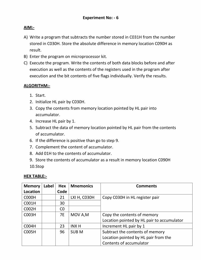
Experiment No: - 6
AIM:-
A) Write a program that subtracts the number stored in C031H from the number
stored in C030H. Store the absolute difference in memory location C090H as
result.
B) Enter the program on microprocessor kit.
C) Execute the program. Write the contents of both data blocks before and after
execution as well as the contents of the registers used in the program after
execution and the bit contents of five flags individually. Verify the results.
ALGORITHM:-
1. Start.
2. Initialize HL pair by C030H.
3. Copy the contents from memory location pointed by HL pair into
accumulator.
4. Increase HL pair by 1.
5. Subtract the data of memory location pointed by HL pair from the contents
of accumulator.
6. If the difference is positive than go to step 9.
7. Complement the content of accumulator.
8. Add 01H to the contents of accumulator.
9. Store the contents of accumulator as a result in memory location C090H
10. Stop
HEX TABLE:-
Memory Location
Label Hex Code
Mnemonics Comments
C000H 21 LXI H, C030H Copy C030H in HL register pair
C001H 30 C002H C0
C003H 7E MOV A,M Copy the contents of memory Location pointed by HL pair to accumulator
C004H 23 INX H Increment HL pair by 1 C005H 96 SUB M Subtract the contents of memory
Location pointed by HL pair from the Contents of accumulator
C006H F2 JP Next Jump If the subtraction result is Positive to Next C007H 0C
C008H C0
C009H 2F CMA Complement the contents of accumulator C00AH C6 ADI 01H Add 01h to the contents of accumulator
C00BH 01
C00CH Next 32 STA C090H Store the contents of accumulator As a result to C090H C00DH 90
C00EH C0 C00FH CF RST 1 Stop
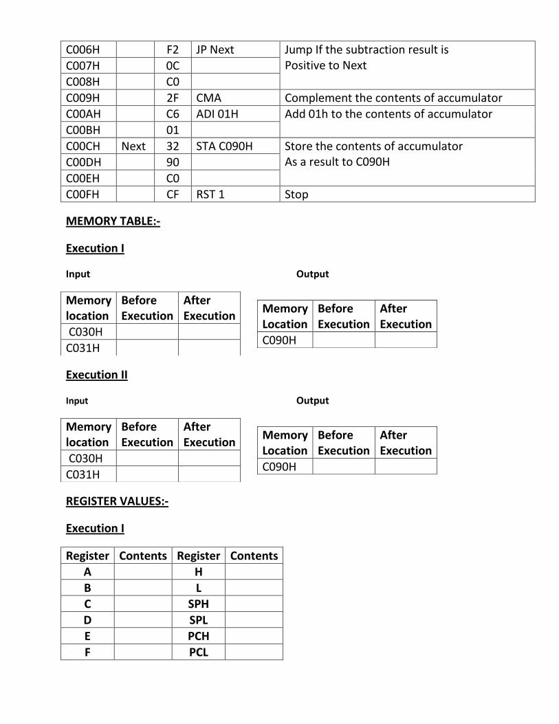
MEMORY TABLE:-
Execution I
Input Output
Execution II
Input Output
REGISTER VALUES:-
Execution I
Register Contents Register Contents A H
B L C SPH
D SPL E PCH
F PCL
Memory location
Before Execution
After Execution
C030H
C031H
Memory Location
Before Execution
After Execution
C090H
Memory location
Before Execution
After Execution
C030H
C031H
Memory Location
Before Execution
After Execution
C090H
FLAG REGISTER:-
S Z X AC X P X CY
Execution II
Register Contents Register Contents A H
B L C SPH
D SPL E PCH
F PCL
FLAG REGISTER:-
S Z X AC X P X CY
CONCLUSION:-
Thus we have executed the program to find the absolute difference.
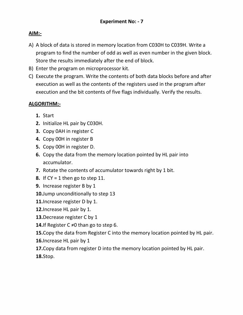
Experiment No: - 7
AIM:-
A) A block of data is stored in memory location from C030H to C039H. Write a
program to find the number of odd as well as even number in the given block.
Store the results immediately after the end of block.
B) Enter the program on microprocessor kit.
C) Execute the program. Write the contents of both data blocks before and after
execution as well as the contents of the registers used in the program after
execution and the bit contents of five flags individually. Verify the results.
ALGORITHM:-
1. Start
2. Initialize HL pair by C030H.
3. Copy 0AH in register C
4. Copy 00H in register B
5. Copy 00H in register D.
6. Copy the data from the memory location pointed by HL pair into
accumulator.
7. Rotate the contents of accumulator towards right by 1 bit.
8. If CY = 1 then go to step 11.
9. Increase register B by 1
10. Jump unconditionally to step 13
11. Increase register D by 1.
12. Increase HL pair by 1.
13. Decrease register C by 1
14. If Register C ≠0 than go to step 6.
15. Copy the data from Register C into the memory location pointed by HL pair.
16. Increase HL pair by 1
17. Copy data from register D into the memory location pointed by HL pair.
18. Stop.
HEX TABLE:-
Memory Location
Label Hex Code
Mnemonics Comments
C000H 21 LXI H, C030H Initialize HL pair with C030H.
C001H 30
C002H C0 C003H 0E MVI C, 0AH Copy 0AH in register C
C004H 0A C005H 06 MVI B,00H Copy 00H in register B
C006H 00
C007H 16 MVI D, 00H Copy 00H in register D
C008H 00
C009H Back 7E MOV A,M Copy the contents of memory Location pointed by HL pair to accumulator
C00AH 0F RRC Rotate the contents of accumulator Towards right by 1 bit
C00BH DA JC Next Jump if CY = 1 to Next
C00CH 12 C00DH C0
C00EH 04 INR B Increment register B by 1 C00FH C3 JMP Skip Jump unconditionally to Skip
C010H 13 C011H C0
C012H Next 14 INR D Increment register D by 1
C013H Skip 23 INXH Increment HL pair by 1 C014H 0D DCR C Decrement register C by 1
C015H C2 JNZ Back Jump if Register C ≠0 C016H 09
C017H C0
C018H 70 MOV M,B Copy the contents of B register To the memory location pointed By HL pair
C019H 23 INX H Increment HL pair by 1
C01AH 72 MOV M,D Copy the contents of D register To the memory location pointed By HL pair
C01BH CF RST 1 Stop
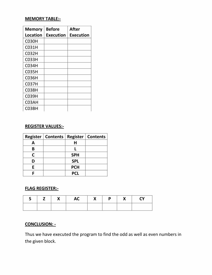
MEMORY TABLE:-
REGISTER VALUES:-
Register Contents Register Contents A H
B L C SPH
D SPL E PCH
F PCL
FLAG REGISTER:-
S Z X AC X P X CY
CONCLUSION: -
Thus we have executed the program to find the odd as well as even numbers in
the given block.
Memory Location
Before Execution
After Execution
C030H C031H
C032H C033H
C034H
C035H C036H
C037H C038H
C039H C03AH
C03BH
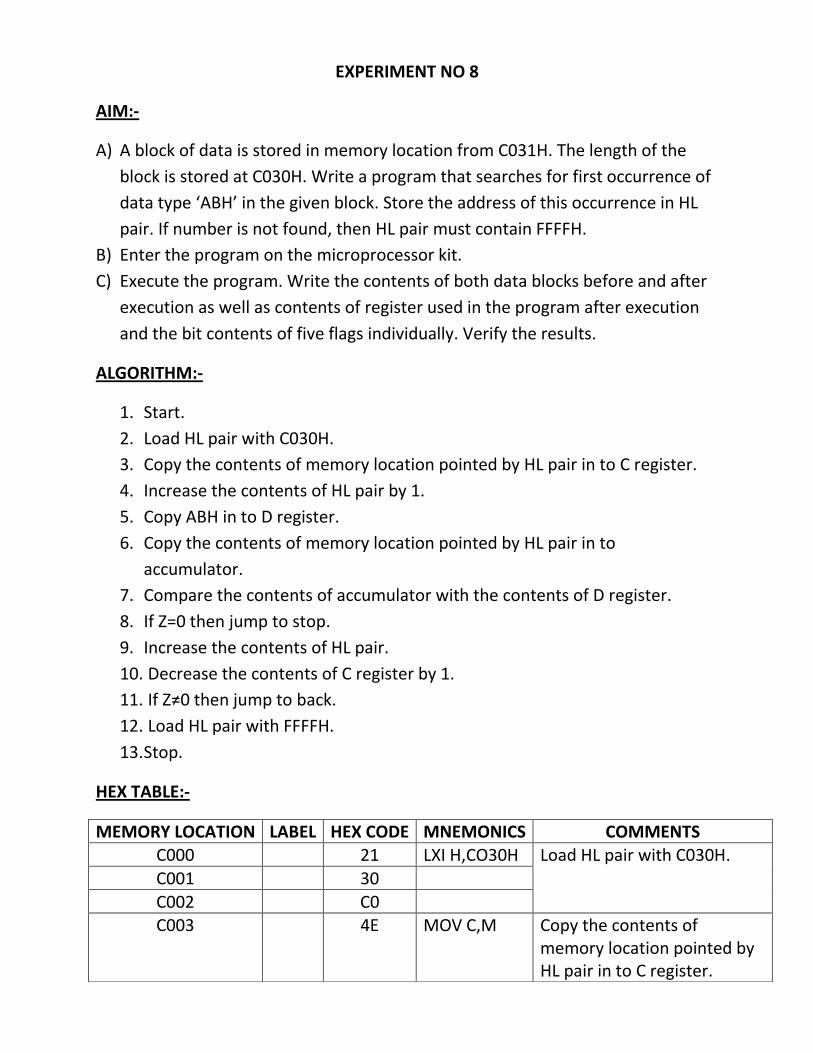
EXPERIMENT NO 8
AIM:-
A) A block of data is stored in memory location from C031H. The length of the
block is stored at C030H. Write a program that searches for first occurrence of
data type ‘ABH’ in the given block. Store the address of this occurrence in HL
pair. If number is not found, then HL pair must contain FFFFH.
B) Enter the program on the microprocessor kit.
C) Execute the program. Write the contents of both data blocks before and after
execution as well as contents of register used in the program after execution
and the bit contents of five flags individually. Verify the results.
ALGORITHM:-
1. Start.
2. Load HL pair with C030H.
3. Copy the contents of memory location pointed by HL pair in to C register.
4. Increase the contents of HL pair by 1.
5. Copy ABH in to D register.
6. Copy the contents of memory location pointed by HL pair in to
accumulator.
7. Compare the contents of accumulator with the contents of D register.
8. If Z=0 then jump to stop.
9. Increase the contents of HL pair.
10. Decrease the contents of C register by 1.
11. If Z≠0 then jump to back.
12. Load HL pair with FFFFH.
13. Stop.
HEX TABLE:-
MEMORY LOCATION LABEL HEX CODE MNEMONICS COMMENTS C000 21 LXI H,CO30H Load HL pair with C030H.
C001 30
C002 C0 C003 4E MOV C,M Copy the contents of
memory location pointed by HL pair in to C register.
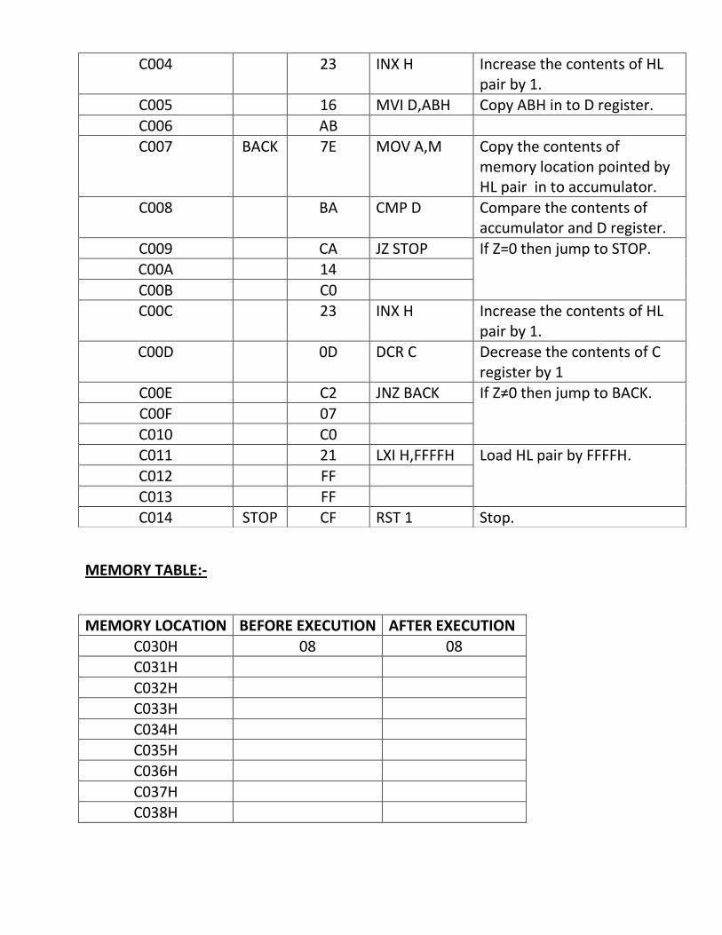
MEMORY TABLE:-
MEMORY LOCATION BEFORE EXECUTION AFTER EXECUTION
C030H 08 08 C031H
C032H C033H
C034H C035H
C036H
C037H C038H
C004 23 INX H Increase the contents of HL pair by 1.
C005 16 MVI D,ABH Copy ABH in to D register.
C006 AB C007 BACK 7E MOV A,M Copy the contents of
memory location pointed by HL pair in to accumulator.
C008 BA CMP D Compare the contents of accumulator and D register.
C009 CA JZ STOP If Z=0 then jump to STOP. C00A 14
C00B C0 C00C 23 INX H Increase the contents of HL
pair by 1. C00D 0D DCR C Decrease the contents of C
register by 1 C00E C2 JNZ BACK If Z≠0 then jump to BACK.
C00F 07
C010 C0 C011 21 LXI H,FFFFH Load HL pair by FFFFH.
C012 FF C013 FF
C014 STOP CF RST 1 Stop.
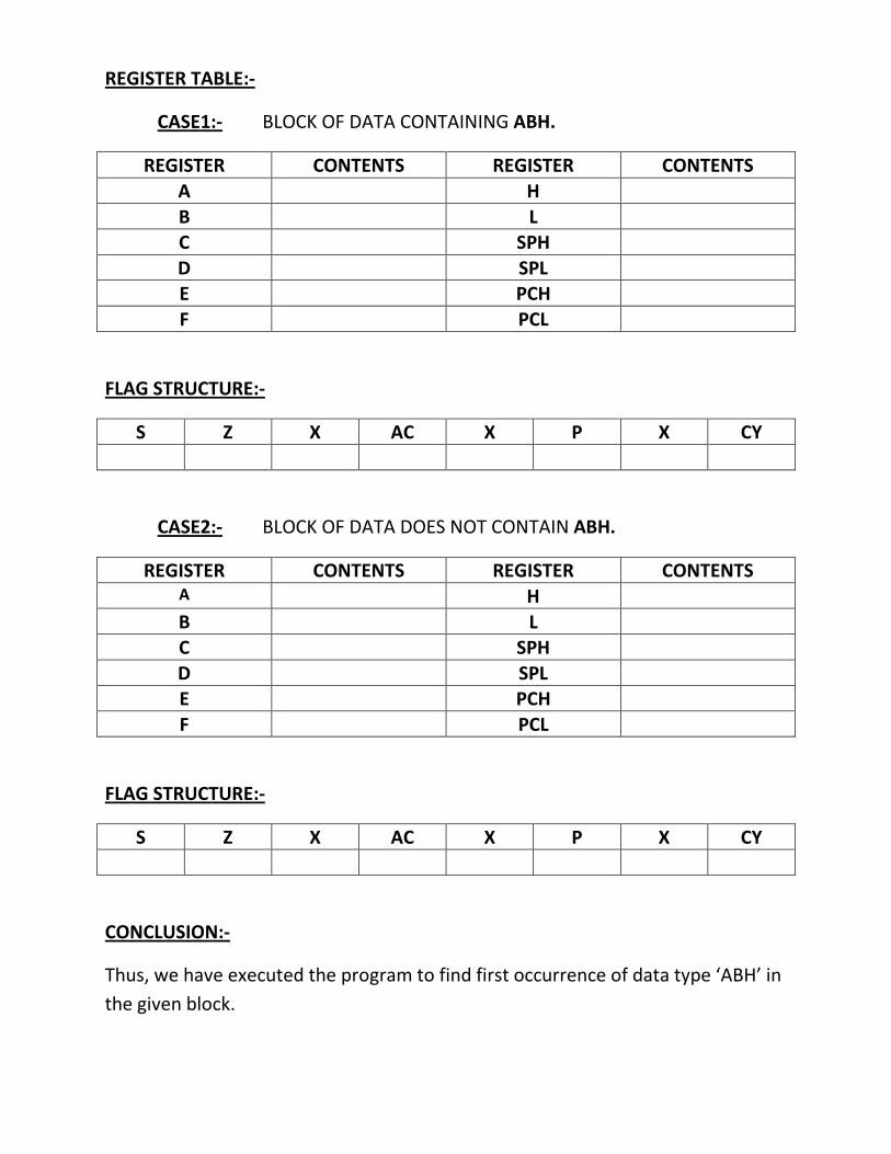
REGISTER TABLE:-
CASE1:- BLOCK OF DATA CONTAINING ABH.
REGISTER CONTENTS REGISTER CONTENTS
A H
B L C SPH
D SPL E PCH
F PCL
FLAG STRUCTURE:-
S Z X AC X P X CY
CASE2:- BLOCK OF DATA DOES NOT CONTAIN ABH.
REGISTER CONTENTS REGISTER CONTENTS A H
B L C SPH
D SPL E PCH
F PCL
FLAG STRUCTURE:-
S Z X AC X P X CY
CONCLUSION:-
Thus, we have executed the program to find first occurrence of data type ‘ABH’ in
the given block.
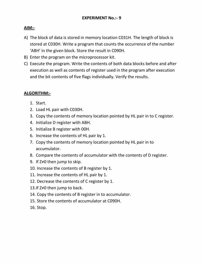
EXPERIMENT No.:- 9
AIM:-
A) The block of data is stored in memory location C031H. The length of block is
stored at C030H. Write a program that counts the occurrence of the number
‘ABH’ in the given block. Store the result in C090H.
B) Enter the program on the microprocessor kit.
C) Execute the program. Write the contents of both data blocks before and after
execution as well as contents of register used in the program after execution
and the bit contents of five flags individually. Verify the results.
ALGORITHM:-
1. Start.
2. Load HL pair with C030H.
3. Copy the contents of memory location pointed by HL pair in to C register.
4. Initialize D register with ABH.
5. Initialize B register with 00H.
6. Increase the contents of HL pair by 1.
7. Copy the contents of memory location pointed by HL pair in to
accumulator.
8. Compare the contents of accumulator with the contents of D register.
9. If Z≠0 then jump to skip.
10. Increase the contents of B register by 1.
11. Increase the contents of HL pair by 1.
12. Decrease the contents of C register by 1.
13. If Z≠0 then jump to back.
14. Copy the contents of B register in to accumulator.
15. Store the contents of accumulator at C090H.
16. Stop.
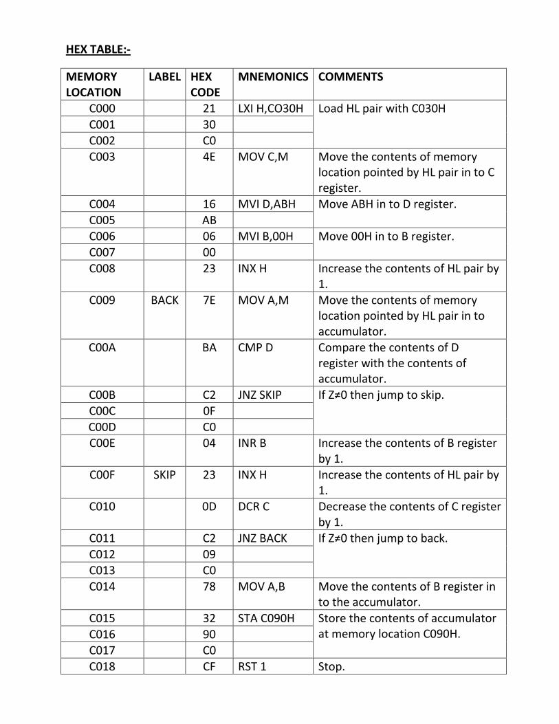
HEX TABLE:-
MEMORY LOCATION
LABEL HEX CODE
MNEMONICS COMMENTS
C000 21 LXI H,CO30H Load HL pair with C030H
C001 30 C002 C0
C003 4E MOV C,M Move the contents of memory location pointed by HL pair in to C register.
C004 16 MVI D,ABH Move ABH in to D register.
C005 AB
C006 06 MVI B,00H Move 00H in to B register. C007 00
C008 23 INX H Increase the contents of HL pair by 1.
C009 BACK 7E MOV A,M Move the contents of memory location pointed by HL pair in to accumulator.
C00A BA CMP D Compare the contents of D register with the contents of accumulator.
C00B C2 JNZ SKIP If Z≠0 then jump to skip. C00C 0F
C00D C0 C00E 04 INR B Increase the contents of B register
by 1. C00F SKIP 23 INX H Increase the contents of HL pair by
1. C010 0D DCR C Decrease the contents of C register
by 1.
C011 C2 JNZ BACK If Z≠0 then jump to back.
C012 09 C013 C0
C014 78 MOV A,B Move the contents of B register in to the accumulator.
C015 32 STA C090H Store the contents of accumulator at memory location C090H. C016 90
C017 C0
C018 CF RST 1 Stop.
MEMORY TABLE:-
MEMORY LOCATION BEFORE EXECUTION AFTER EXECUTION
C030 08 08 C031
C032
C033 C034
C035 C036
C037
C038
REGISTER TABLE:-
REGISTER CONTENTS REGISTER CONTENTS
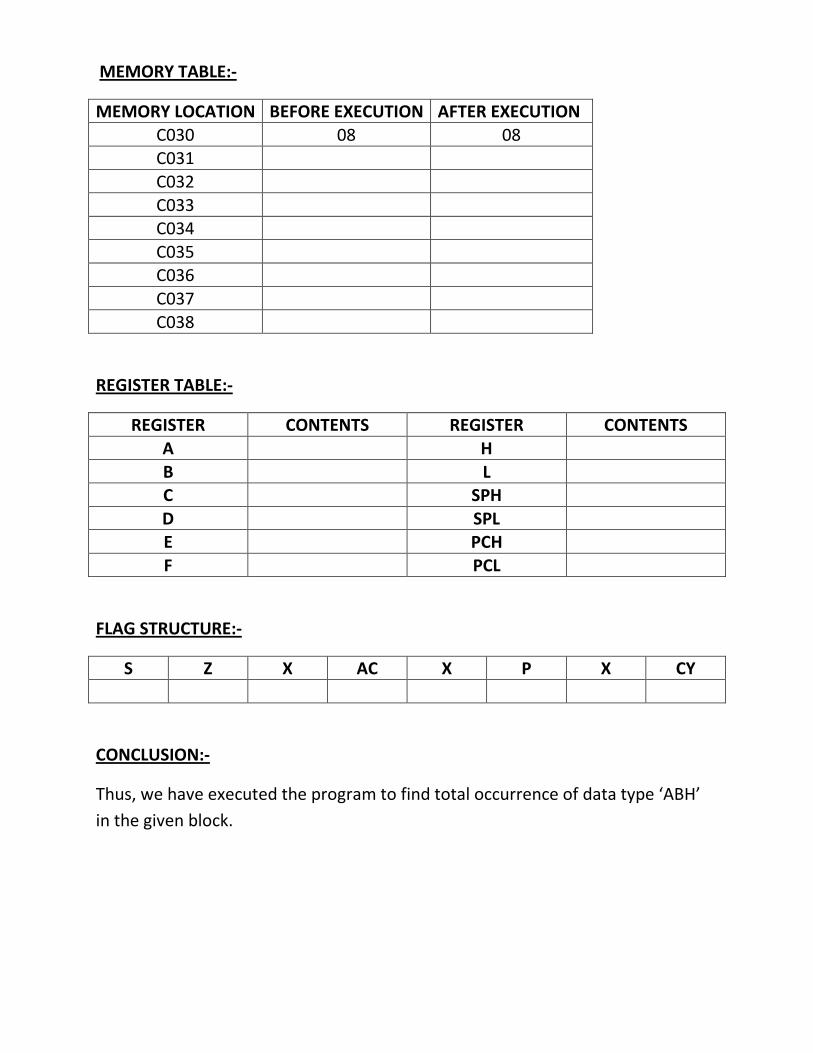
A H
B L C SPH
D SPL E PCH
F PCL
FLAG STRUCTURE:-
S Z X AC X P X CY
CONCLUSION:-
Thus, we have executed the program to find total occurrence of data type ‘ABH’
in the given block.
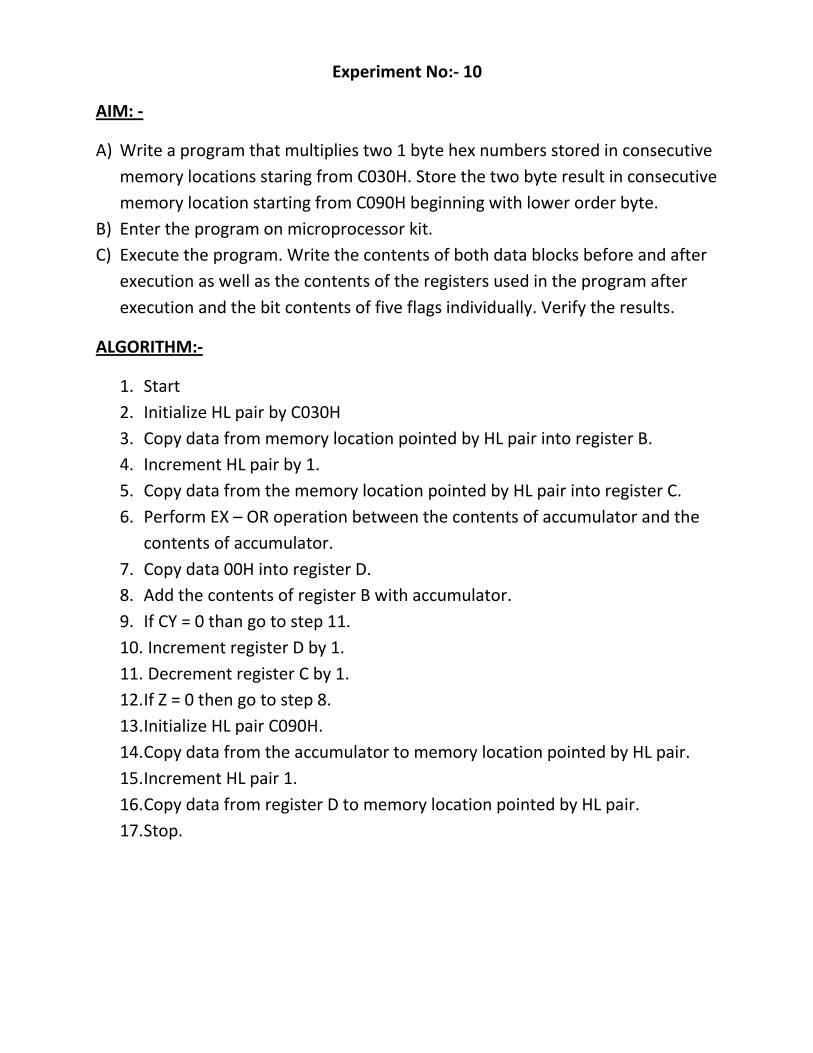
Experiment No:- 10
AIM: -
A) Write a program that multiplies two 1 byte hex numbers stored in consecutive
memory locations staring from C030H. Store the two byte result in consecutive
memory location starting from C090H beginning with lower order byte.
B) Enter the program on microprocessor kit.
C) Execute the program. Write the contents of both data blocks before and after
execution as well as the contents of the registers used in the program after
execution and the bit contents of five flags individually. Verify the results.
ALGORITHM:-
1. Start
2. Initialize HL pair by C030H
3. Copy data from memory location pointed by HL pair into register B.
4. Increment HL pair by 1.
5. Copy data from the memory location pointed by HL pair into register C.
6. Perform EX – OR operation between the contents of accumulator and the
contents of accumulator.
7. Copy data 00H into register D.
8. Add the contents of register B with accumulator.
9. If CY = 0 than go to step 11.
10. Increment register D by 1.
11. Decrement register C by 1.
12. If Z = 0 then go to step 8.
13. Initialize HL pair C090H.
14. Copy data from the accumulator to memory location pointed by HL pair.
15. Increment HL pair 1.
16. Copy data from register D to memory location pointed by HL pair.
17. Stop.
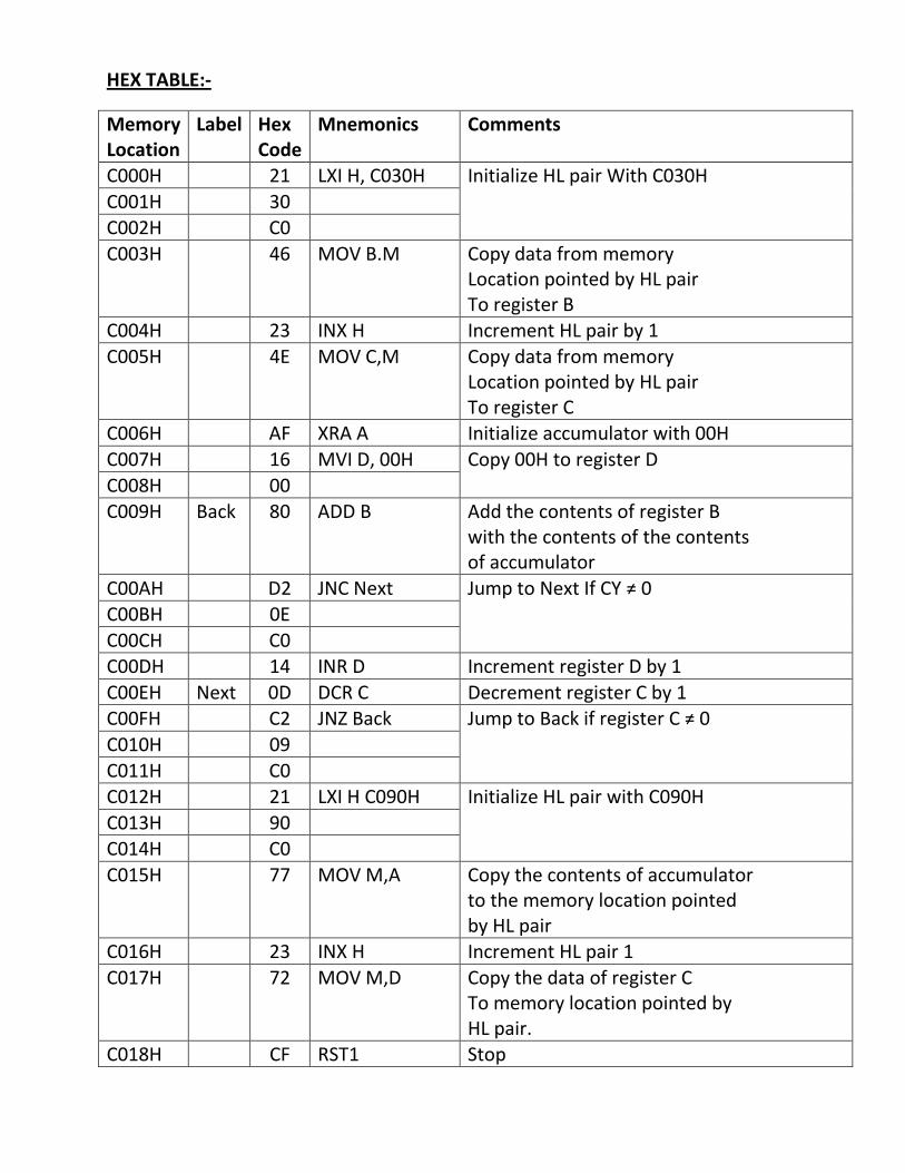
HEX TABLE:-
Memory Location
Label Hex Code
Mnemonics Comments
C000H 21 LXI H, C030H Initialize HL pair With C030H
C001H 30 C002H C0
C003H 46 MOV B.M Copy data from memory Location pointed by HL pair To register B
C004H 23 INX H Increment HL pair by 1
C005H 4E MOV C,M Copy data from memory Location pointed by HL pair To register C
C006H AF XRA A Initialize accumulator with 00H
C007H 16 MVI D, 00H Copy 00H to register D
C008H 00 C009H Back 80 ADD B Add the contents of register B
with the contents of the contents of accumulator
C00AH D2 JNC Next Jump to Next If CY ≠ 0 C00BH 0E
C00CH C0 C00DH 14 INR D Increment register D by 1
C00EH Next 0D DCR C Decrement register C by 1 C00FH C2 JNZ Back Jump to Back if register C ≠ 0
C010H 09
C011H C0 C012H 21 LXI H C090H Initialize HL pair with C090H
C013H 90 C014H C0
C015H 77 MOV M,A Copy the contents of accumulator to the memory location pointed by HL pair
C016H 23 INX H Increment HL pair 1
C017H 72 MOV M,D Copy the data of register C To memory location pointed by HL pair.
C018H CF RST1 Stop
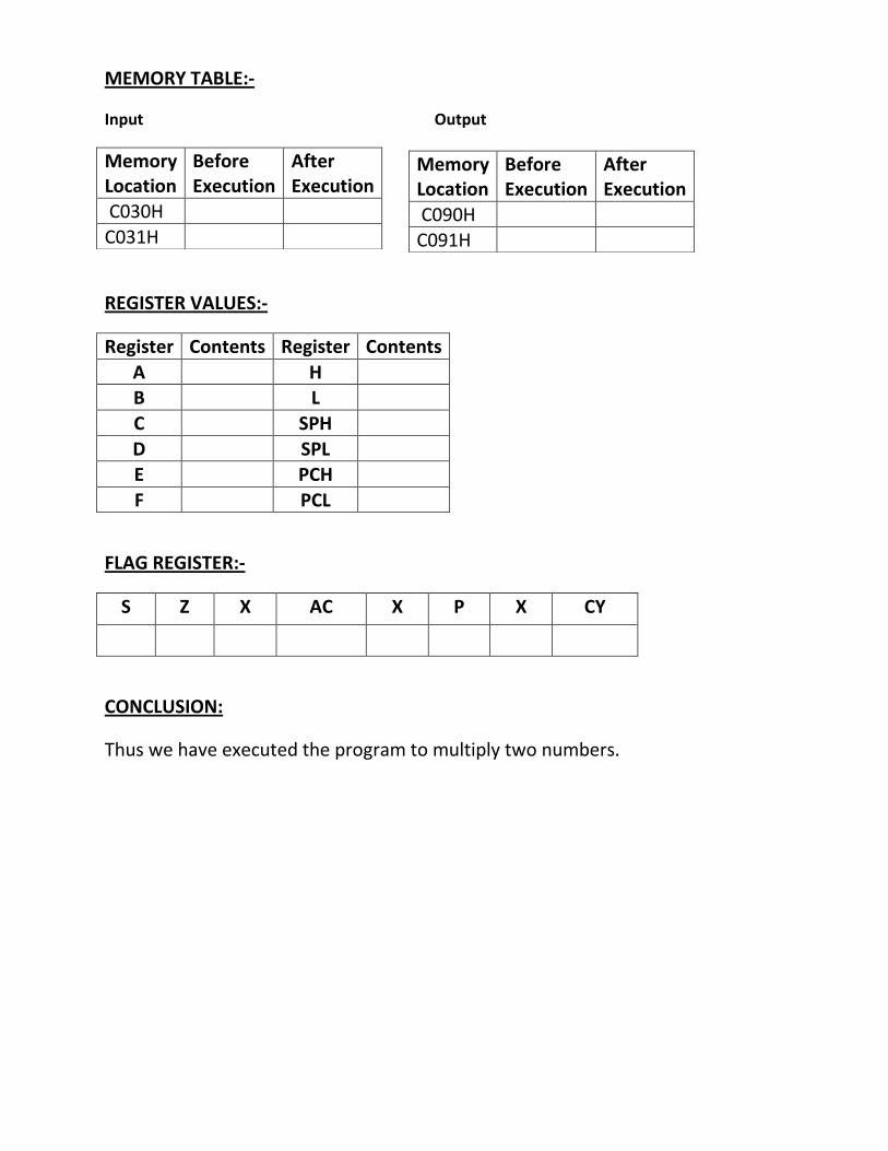
MEMORY TABLE:-
Input Output
REGISTER VALUES:-
Register Contents Register Contents
A H B L
C SPH
D SPL E PCH
F PCL
FLAG REGISTER:-
S Z X AC X P X CY
CONCLUSION:
Thus we have executed the program to multiply two numbers.
Memory Location
Before Execution
After Execution
C030H
C031H
Memory Location
Before Execution
After Execution
C090H C091H
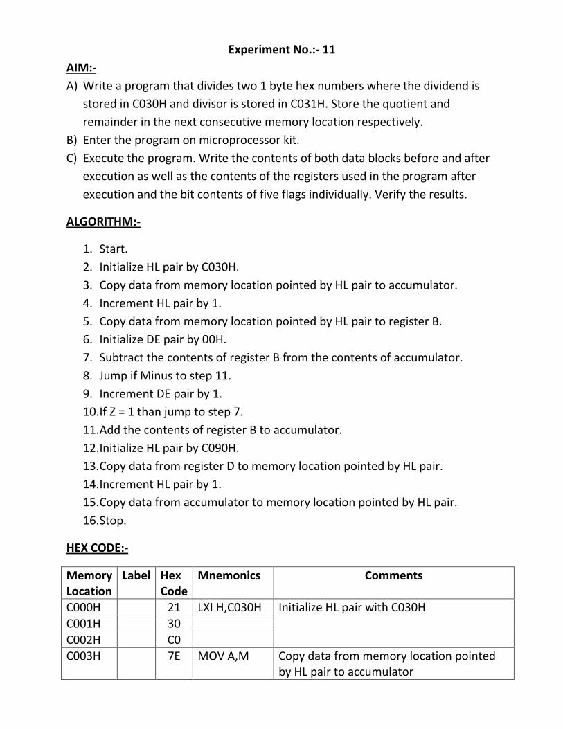
Experiment No.:- 11
AIM:-
A) Write a program that divides two 1 byte hex numbers where the dividend is
stored in C030H and divisor is stored in C031H. Store the quotient and
remainder in the next consecutive memory location respectively.
B) Enter the program on microprocessor kit.
C) Execute the program. Write the contents of both data blocks before and after
execution as well as the contents of the registers used in the program after
execution and the bit contents of five flags individually. Verify the results.
ALGORITHM:-
1. Start.
2. Initialize HL pair by C030H.
3. Copy data from memory location pointed by HL pair to accumulator.
4. Increment HL pair by 1.
5. Copy data from memory location pointed by HL pair to register B.
6. Initialize DE pair by 00H.
7. Subtract the contents of register B from the contents of accumulator.
8. Jump if Minus to step 11.
9. Increment DE pair by 1.
10. If Z = 1 than jump to step 7.
11. Add the contents of register B to accumulator.
12. Initialize HL pair by C090H.
13. Copy data from register D to memory location pointed by HL pair.
14. Increment HL pair by 1.
15. Copy data from accumulator to memory location pointed by HL pair.
16. Stop.
HEX CODE:-
Memory Location
Label Hex Code
Mnemonics Comments
C000H 21 LXI H,C030H Initialize HL pair with C030H
C001H 30
C002H C0 C003H 7E MOV A,M Copy data from memory location pointed
by HL pair to accumulator
C004H 23 INX H Increment HL pair by 1
C005H 46 MOV B,M Copy data from memory location pointed by HL pair to register B
C006H 16 MVI D, 00H Copy 00H to register D C007H 00
C008H Back 90 SUB B Subtract the contents of register B from the contents of accumulator
C009H FA JM Next Jump if Minus to Next C00AH 10
C00BH C0
C00CH 14 INR D Increment register D by 1 C00DH C3 JMP Back Jump unconditionally to Back
C00EH 08 C00FH C0
C010H Next 80 ADD B Add the contents of register B with the contents Of accumulator.
C011H 21 LXIH,C090H Initialize HL pair with C090H
C012H 90
C013H C0 C014H 72 MOV M,D Copy the contents of register D to memory
location pointed by HL pair C015H 23 INX H Increment Hl pair by 1
C016H 77 MOV M,A Copy the contents of accumulator to memory location pointed by HL pair
C017H CF RST 1 Stop
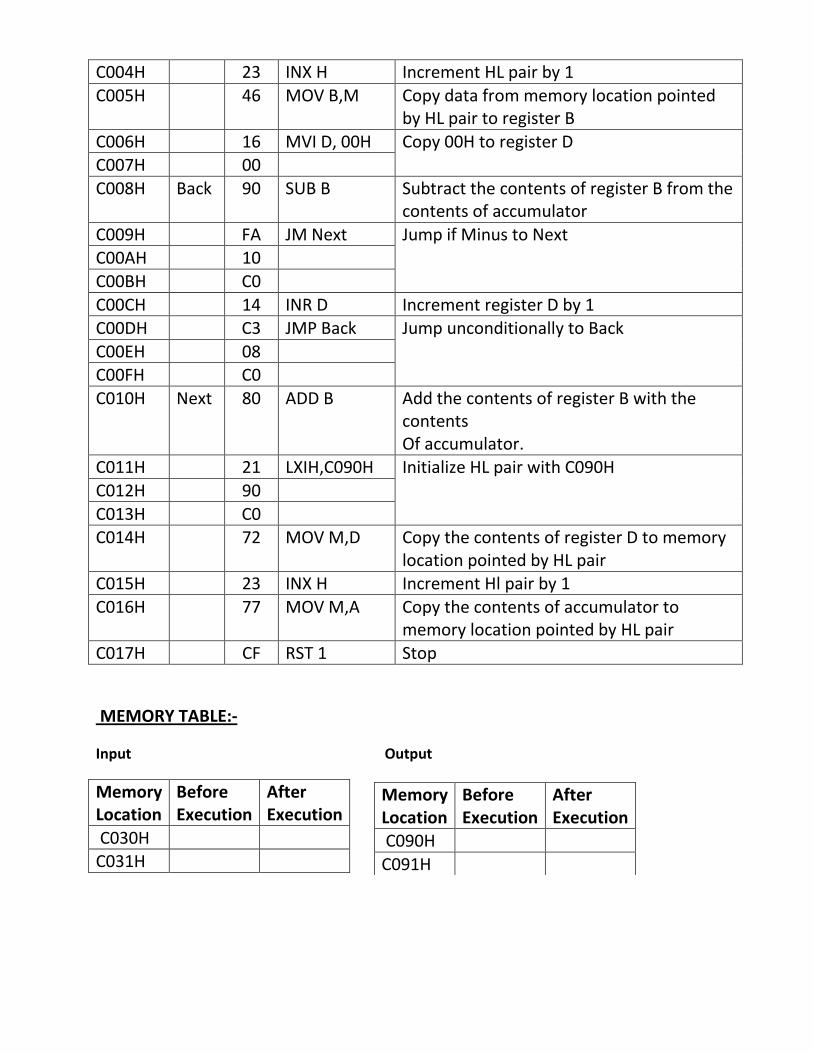
MEMORY TABLE:-
Input Output
Memory Location
Before Execution
After Execution
C030H C031H
Memory Location
Before Execution
After Execution
C090H
C091H
REGISTER VALUES:-
Register Contents Register Contents
A H B L
C SPH
D SPL E PCH
F PCL
FLAG REGISTER:-
S Z X AC X P X CY
CONCLUSION:
Thus we have executed the program to divide first number by second number.
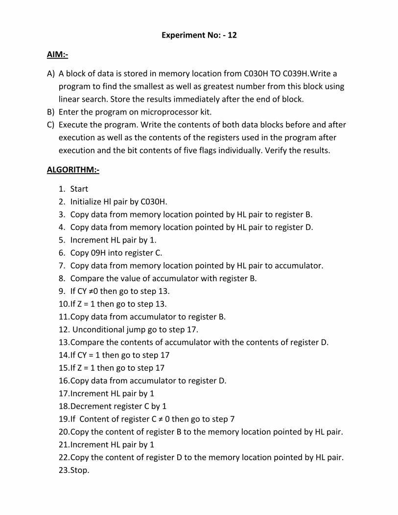
Experiment No: - 12
AIM:-
A) A block of data is stored in memory location from C030H TO C039H.Write a
program to find the smallest as well as greatest number from this block using
linear search. Store the results immediately after the end of block.
B) Enter the program on microprocessor kit.
C) Execute the program. Write the contents of both data blocks before and after
execution as well as the contents of the registers used in the program after
execution and the bit contents of five flags individually. Verify the results.
ALGORITHM:-
1. Start
2. Initialize Hl pair by C030H.
3. Copy data from memory location pointed by HL pair to register B.
4. Copy data from memory location pointed by HL pair to register D.
5. Increment HL pair by 1.
6. Copy 09H into register C.
7. Copy data from memory location pointed by HL pair to accumulator.
8. Compare the value of accumulator with register B.
9. If CY ≠0 then go to step 13.
10. If Z = 1 then go to step 13.
11. Copy data from accumulator to register B.
12. Unconditional jump go to step 17.
13. Compare the contents of accumulator with the contents of register D.
14. If CY = 1 then go to step 17
15. If Z = 1 then go to step 17
16. Copy data from accumulator to register D.
17. Increment HL pair by 1
18. Decrement register C by 1
19. If Content of register C ≠ 0 then go to step 7
20. Copy the content of register B to the memory location pointed by HL pair.
21. Increment HL pair by 1
22. Copy the content of register D to the memory location pointed by HL pair.
23. Stop.
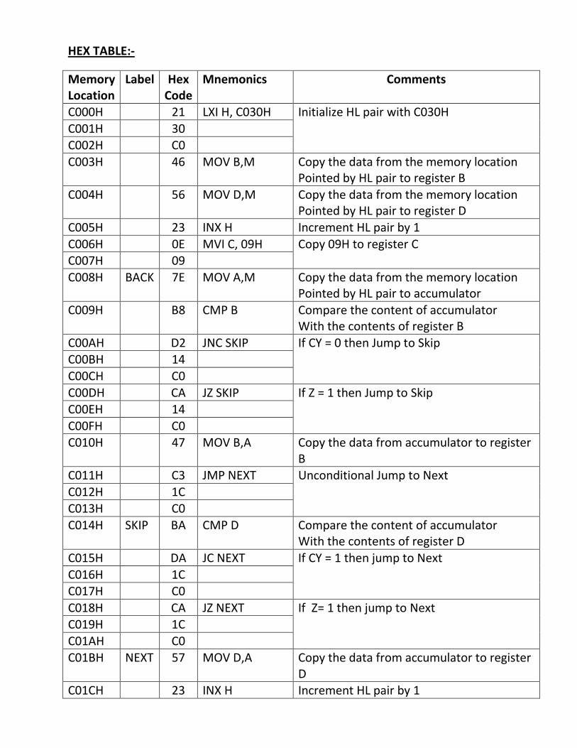
HEX TABLE:-
Memory Location
Label Hex Code
Mnemonics Comments
C000H 21 LXI H, C030H Initialize HL pair with C030H
C001H 30 C002H C0
C003H 46 MOV B,M Copy the data from the memory location Pointed by HL pair to register B
C004H 56 MOV D,M Copy the data from the memory location Pointed by HL pair to register D
C005H 23 INX H Increment HL pair by 1
C006H 0E MVI C, 09H Copy 09H to register C C007H 09
C008H BACK 7E MOV A,M Copy the data from the memory location Pointed by HL pair to accumulator
C009H B8 CMP B Compare the content of accumulator With the contents of register B
C00AH D2 JNC SKIP If CY = 0 then Jump to Skip C00BH 14
C00CH C0
C00DH CA JZ SKIP If Z = 1 then Jump to Skip C00EH 14
C00FH C0 C010H 47 MOV B,A Copy the data from accumulator to register
B C011H C3 JMP NEXT Unconditional Jump to Next
C012H 1C C013H C0
C014H SKIP BA CMP D Compare the content of accumulator With the contents of register D
C015H DA JC NEXT If CY = 1 then jump to Next
C016H 1C C017H C0
C018H CA JZ NEXT If Z= 1 then jump to Next C019H 1C
C01AH C0 C01BH NEXT 57 MOV D,A Copy the data from accumulator to register
D C01CH 23 INX H Increment HL pair by 1
C01DH 0D DCR C Decrement register C by 1
C01EH C2 JNZ BACK If the content of register C ≠ 0 then jump to back C01FH 08
C020H C0 C021H 70 MOV M,B Copy the data from register B to memory
Location Pointed by HL pair C022H 23 INX H Increment HL pair by 1
C023H 72 MOV M,D Copy the data from register D to the memory location Pointed by HL pair
C024H CF RST 1 Stop
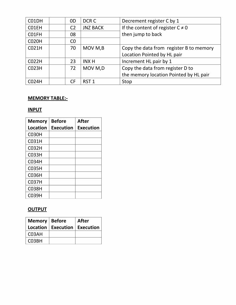
MEMORY TABLE:-
INPUT
OUTPUT
Memory Location
Before Execution
After Execution
C030H
C031H
C032H C033H
C034H C035H
C036H
C037H C038H
C039H
Memory Location
Before Execution
After Execution
C03AH C03BH
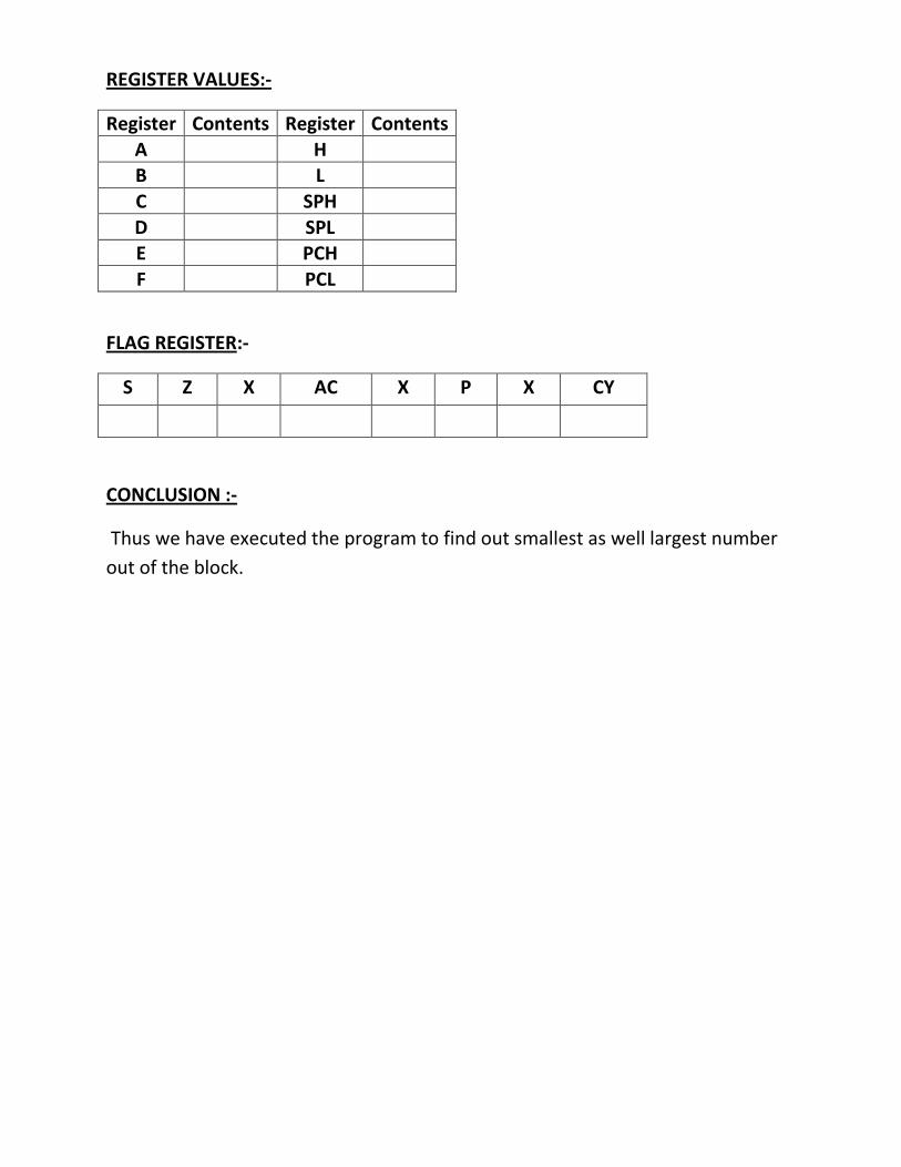
REGISTER VALUES:-
Register Contents Register Contents
A H B L
C SPH
D SPL E PCH
F PCL
FLAG REGISTER:-
S Z X AC X P X CY
CONCLUSION :-
Thus we have executed the program to find out smallest as well largest number
out of the block.
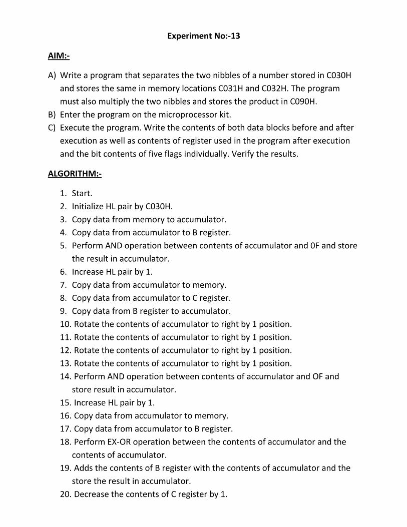
Experiment No:-13
AIM:-
A) Write a program that separates the two nibbles of a number stored in C030H
and stores the same in memory locations C031H and C032H. The program
must also multiply the two nibbles and stores the product in C090H.
B) Enter the program on the microprocessor kit.
C) Execute the program. Write the contents of both data blocks before and after
execution as well as contents of register used in the program after execution
and the bit contents of five flags individually. Verify the results.
ALGORITHM:-
1. Start.
2. Initialize HL pair by C030H.
3. Copy data from memory to accumulator.
4. Copy data from accumulator to B register.
5. Perform AND operation between contents of accumulator and 0F and store
the result in accumulator.
6. Increase HL pair by 1.
7. Copy data from accumulator to memory.
8. Copy data from accumulator to C register.
9. Copy data from B register to accumulator.
10. Rotate the contents of accumulator to right by 1 position.
11. Rotate the contents of accumulator to right by 1 position.
12. Rotate the contents of accumulator to right by 1 position.
13. Rotate the contents of accumulator to right by 1 position.
14. Perform AND operation between contents of accumulator and OF and
store result in accumulator.
15. Increase HL pair by 1.
16. Copy data from accumulator to memory.
17. Copy data from accumulator to B register.
18. Perform EX-OR operation between the contents of accumulator and the
contents of accumulator.
19. Adds the contents of B register with the contents of accumulator and the
store the result in accumulator.
20. Decrease the contents of C register by 1.
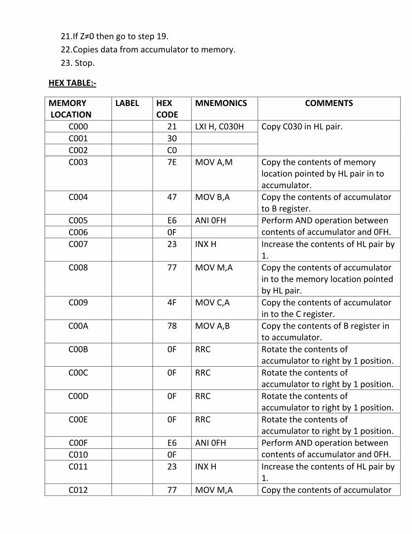
21. If Z≠0 then go to step 19.
22. Copies data from accumulator to memory.
23. Stop.
HEX TABLE:-
MEMORY LOCATION
LABEL HEX CODE
MNEMONICS COMMENTS
C000 21 LXI H, C030H Copy C030 in HL pair.
C001 30 C002 C0
C003 7E MOV A,M Copy the contents of memory location pointed by HL pair in to accumulator.
C004 47 MOV B,A Copy the contents of accumulator to B register.
C005 E6 ANI 0FH Perform AND operation between contents of accumulator and 0FH. C006 0F
C007 23 INX H Increase the contents of HL pair by 1.
C008 77 MOV M,A Copy the contents of accumulator in to the memory location pointed by HL pair.
C009 4F MOV C,A Copy the contents of accumulator in to the C register.
C00A 78 MOV A,B Copy the contents of B register in to accumulator.
C00B 0F RRC Rotate the contents of accumulator to right by 1 position.
C00C 0F RRC Rotate the contents of accumulator to right by 1 position.
C00D 0F RRC Rotate the contents of accumulator to right by 1 position.
C00E 0F RRC Rotate the contents of accumulator to right by 1 position.
C00F E6 ANI 0FH Perform AND operation between contents of accumulator and 0FH. C010 0F
C011 23 INX H Increase the contents of HL pair by 1.
C012 77 MOV M,A Copy the contents of accumulator
in to the memory location pointed by HL pair.
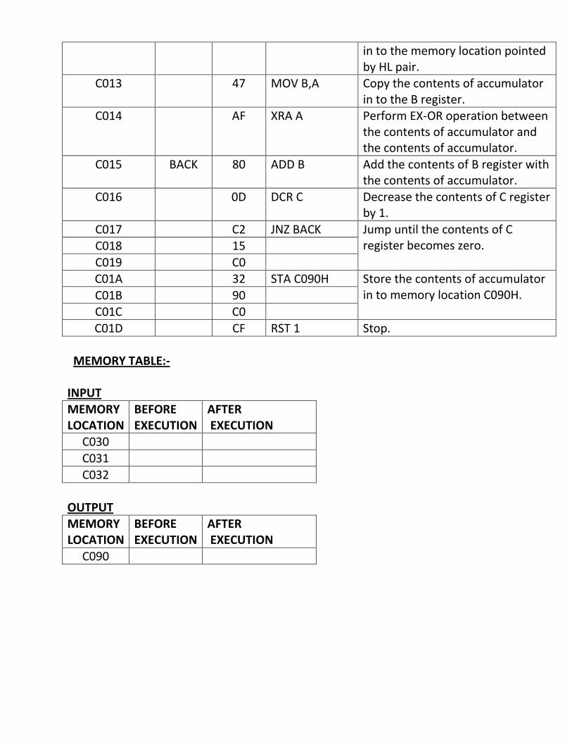
C013 47 MOV B,A Copy the contents of accumulator in to the B register.
C014 AF XRA A Perform EX-OR operation between the contents of accumulator and the contents of accumulator.
C015 BACK 80 ADD B Add the contents of B register with the contents of accumulator.
C016 0D DCR C Decrease the contents of C register by 1.
C017 C2 JNZ BACK Jump until the contents of C register becomes zero. C018 15
C019 C0 C01A 32 STA C090H Store the contents of accumulator
in to memory location C090H. C01B 90 C01C C0
C01D CF RST 1 Stop.
MEMORY TABLE:- INPUT MEMORY LOCATION
BEFORE EXECUTION
AFTER EXECUTION
C030
C031
C032 OUTPUT MEMORY LOCATION
BEFORE EXECUTION
AFTER EXECUTION
C090

REGISTER TABLE:-
REGISTER CONTENTS REGISTER CONTENTS
A H B L
C SPH
D SPL E PCH
F PCL
FLAG STRUCTURE:-
S Z X AC X P X CY
CONCLUSION:-
Thus, we have executed the program to separate two nibbles of a number and
multiply them.
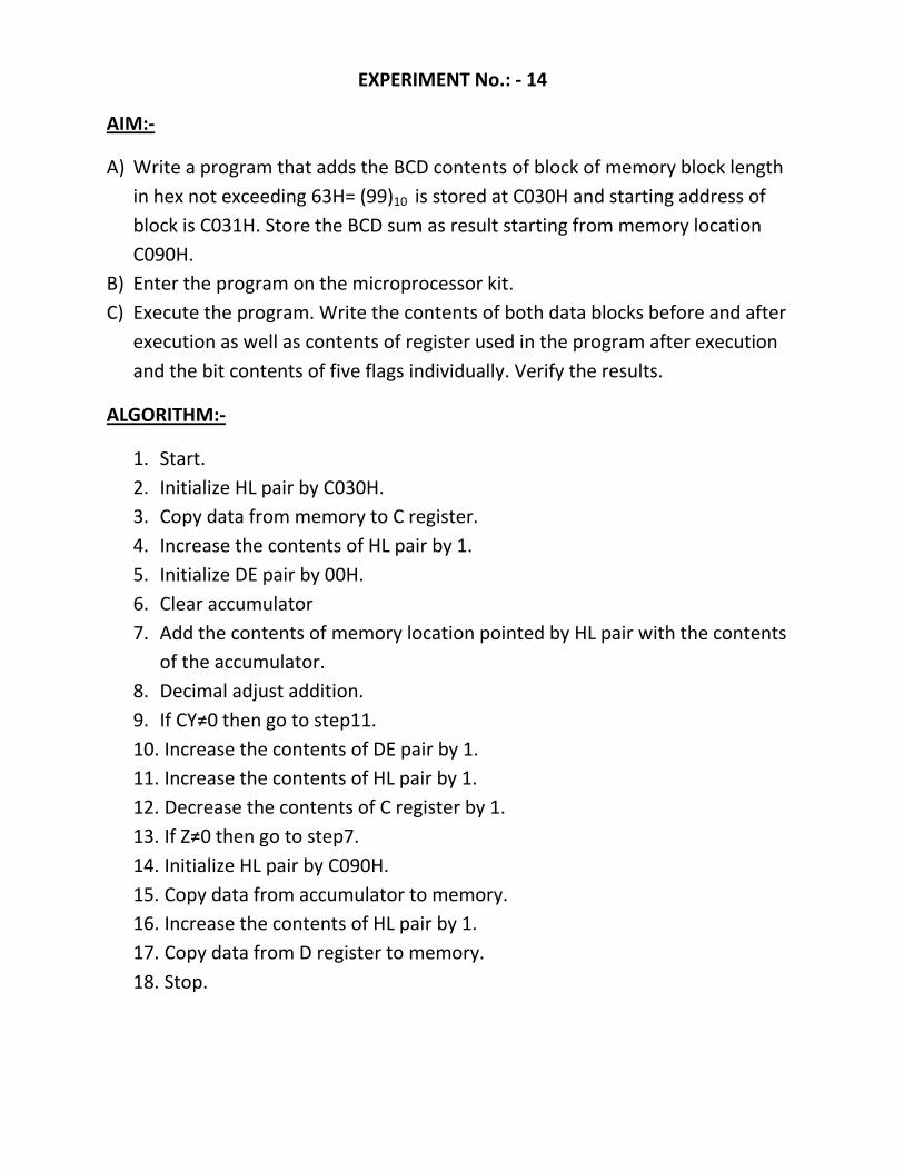
EXPERIMENT No.: - 14
AIM:-
A) Write a program that adds the BCD contents of block of memory block length
in hex not exceeding 63H= (99)10 is stored at C030H and starting address of
block is C031H. Store the BCD sum as result starting from memory location
C090H.
B) Enter the program on the microprocessor kit.
C) Execute the program. Write the contents of both data blocks before and after
execution as well as contents of register used in the program after execution
and the bit contents of five flags individually. Verify the results.
ALGORITHM:-
1. Start.
2. Initialize HL pair by C030H.
3. Copy data from memory to C register.
4. Increase the contents of HL pair by 1.
5. Initialize DE pair by 00H.
6. Clear accumulator
7. Add the contents of memory location pointed by HL pair with the contents
of the accumulator.
8. Decimal adjust addition.
9. If CY≠0 then go to step11.
10. Increase the contents of DE pair by 1.
11. Increase the contents of HL pair by 1.
12. Decrease the contents of C register by 1.
13. If Z≠0 then go to step7.
14. Initialize HL pair by C090H.
15. Copy data from accumulator to memory.
16. Increase the contents of HL pair by 1.
17. Copy data from D register to memory.
18. Stop.
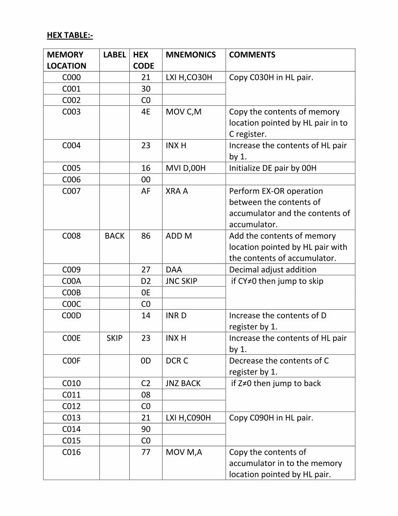
HEX TABLE:-
MEMORY LOCATION
LABEL HEX CODE
MNEMONICS COMMENTS
C000 21 LXI H,CO30H Copy C030H in HL pair.
C001 30 C002 C0
C003 4E MOV C,M Copy the contents of memory location pointed by HL pair in to C register.
C004 23 INX H Increase the contents of HL pair by 1.
C005 16 MVI D,00H Initialize DE pair by 00H
C006 00
C007 AF XRA A Perform EX-OR operation between the contents of accumulator and the contents of accumulator.
C008 BACK 86 ADD M Add the contents of memory location pointed by HL pair with the contents of accumulator.
C009 27 DAA Decimal adjust addition C00A D2 JNC SKIP if CY≠0 then jump to skip
C00B 0E
C00C C0 C00D 14 INR D Increase the contents of D
register by 1. C00E SKIP 23 INX H Increase the contents of HL pair
by 1. C00F 0D DCR C Decrease the contents of C
register by 1.
C010 C2 JNZ BACK if Z≠0 then jump to back
C011 08 C012 C0
C013 21 LXI H,C090H Copy C090H in HL pair. C014 90
C015 C0
C016 77 MOV M,A Copy the contents of accumulator in to the memory location pointed by HL pair.
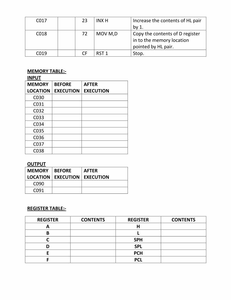
C017 23 INX H Increase the contents of HL pair by 1.
C018 72 MOV M,D Copy the contents of D register in to the memory location pointed by HL pair.
C019 CF RST 1 Stop.
MEMORY TABLE:- INPUT MEMORY LOCATION
BEFORE EXECUTION
AFTER EXECUTION
C030
C031 C032
C033
C034 C035
C036 C037
C038
OUTPUT
MEMORY LOCATION
BEFORE EXECUTION
AFTER EXECUTION
C090
C091
REGISTER TABLE:-
REGISTER CONTENTS REGISTER CONTENTS
A H B L
C SPH D SPL
E PCH
F PCL
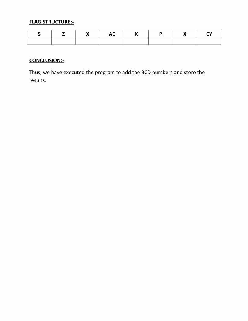
FLAG STRUCTURE:-
S Z X AC X P X CY
CONCLUSION:-
Thus, we have executed the program to add the BCD numbers and store the
results.
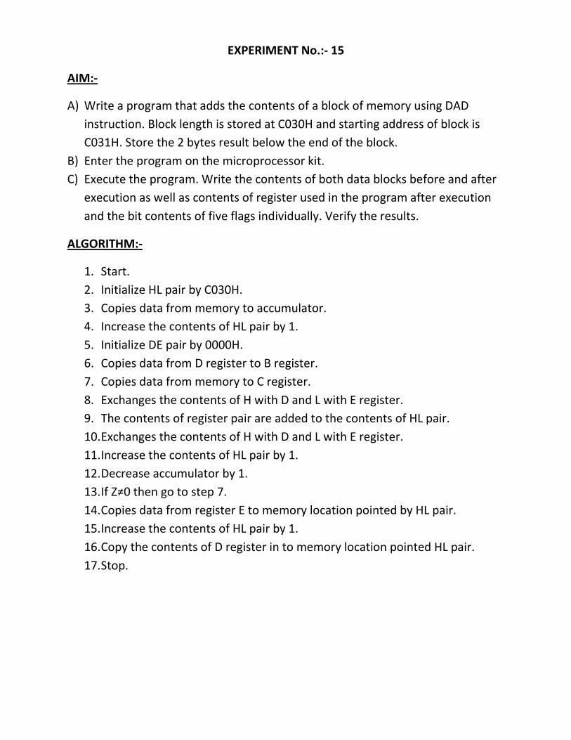
EXPERIMENT No.:- 15
AIM:-
A) Write a program that adds the contents of a block of memory using DAD
instruction. Block length is stored at C030H and starting address of block is
C031H. Store the 2 bytes result below the end of the block.
B) Enter the program on the microprocessor kit.
C) Execute the program. Write the contents of both data blocks before and after
execution as well as contents of register used in the program after execution
and the bit contents of five flags individually. Verify the results.
ALGORITHM:-
1. Start.
2. Initialize HL pair by C030H.
3. Copies data from memory to accumulator.
4. Increase the contents of HL pair by 1.
5. Initialize DE pair by 0000H.
6. Copies data from D register to B register.
7. Copies data from memory to C register.
8. Exchanges the contents of H with D and L with E register.
9. The contents of register pair are added to the contents of HL pair.
10. Exchanges the contents of H with D and L with E register.
11. Increase the contents of HL pair by 1.
12. Decrease accumulator by 1.
13. If Z≠0 then go to step 7.
14. Copies data from register E to memory location pointed by HL pair.
15. Increase the contents of HL pair by 1.
16. Copy the contents of D register in to memory location pointed HL pair.
17. Stop.
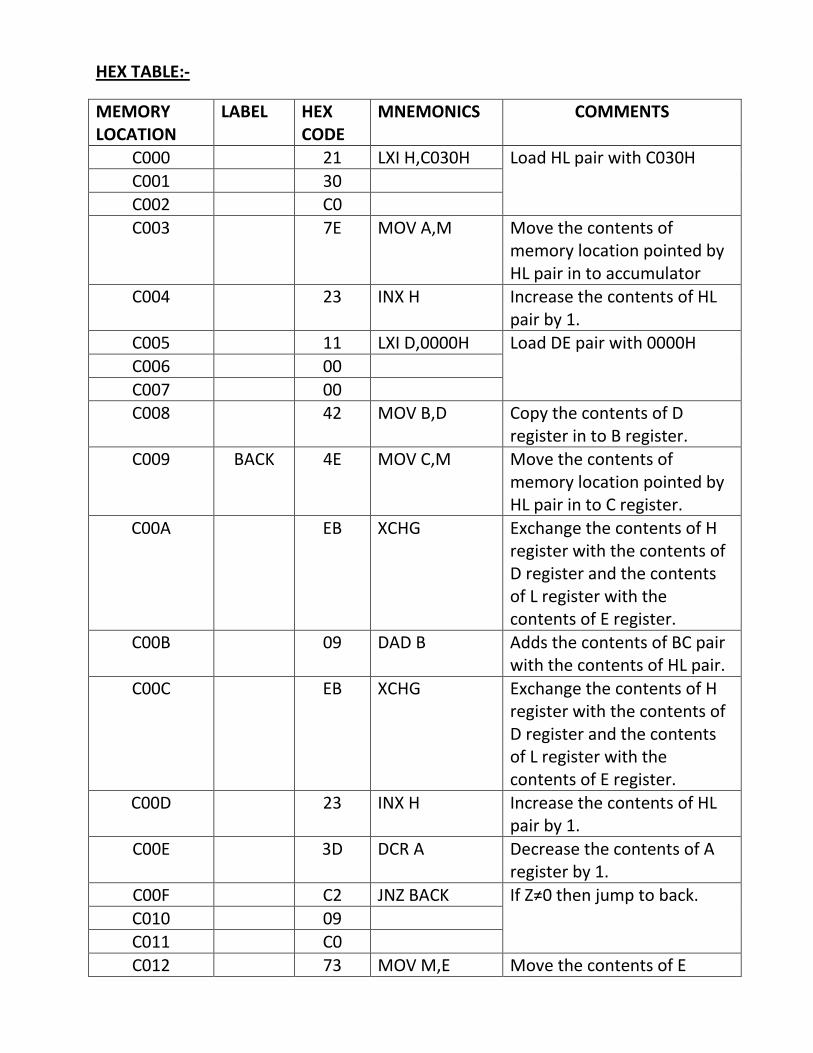
HEX TABLE:-
MEMORY LOCATION
LABEL HEX CODE
MNEMONICS COMMENTS
C000 21 LXI H,C030H Load HL pair with C030H
C001 30 C002 C0
C003 7E MOV A,M Move the contents of memory location pointed by HL pair in to accumulator
C004 23 INX H Increase the contents of HL pair by 1.
C005 11 LXI D,0000H Load DE pair with 0000H
C006 00
C007 00 C008 42 MOV B,D Copy the contents of D
register in to B register. C009 BACK 4E MOV C,M Move the contents of
memory location pointed by HL pair in to C register.
C00A EB XCHG Exchange the contents of H register with the contents of D register and the contents of L register with the contents of E register.
C00B 09 DAD B Adds the contents of BC pair with the contents of HL pair.
C00C EB XCHG Exchange the contents of H register with the contents of D register and the contents of L register with the contents of E register.
C00D 23 INX H Increase the contents of HL pair by 1.
C00E 3D DCR A Decrease the contents of A register by 1.
C00F C2 JNZ BACK If Z≠0 then jump to back.
C010 09 C011 C0
C012 73 MOV M,E Move the contents of E
register in to the memory location pointed by HL pair.
C013 23 INX H Increase the contents of HL pair by 1.
C014 72 MOV M,D Move the contents of D register in to the memory location pointed by HL pair.
C015 CF RST1 Stop.
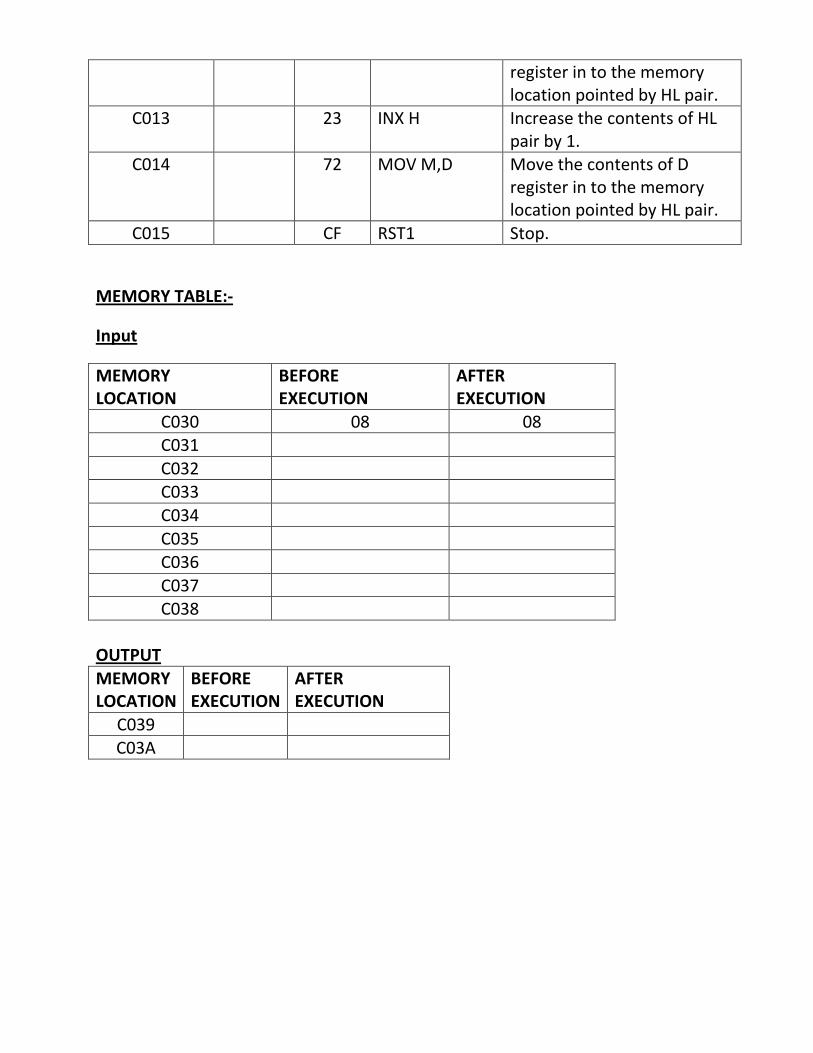
MEMORY TABLE:-
Input
MEMORY LOCATION
BEFORE EXECUTION
AFTER EXECUTION
C030 08 08 C031
C032 C033
C034
C035 C036
C037 C038
OUTPUT
MEMORY LOCATION
BEFORE EXECUTION
AFTER EXECUTION
C039 C03A
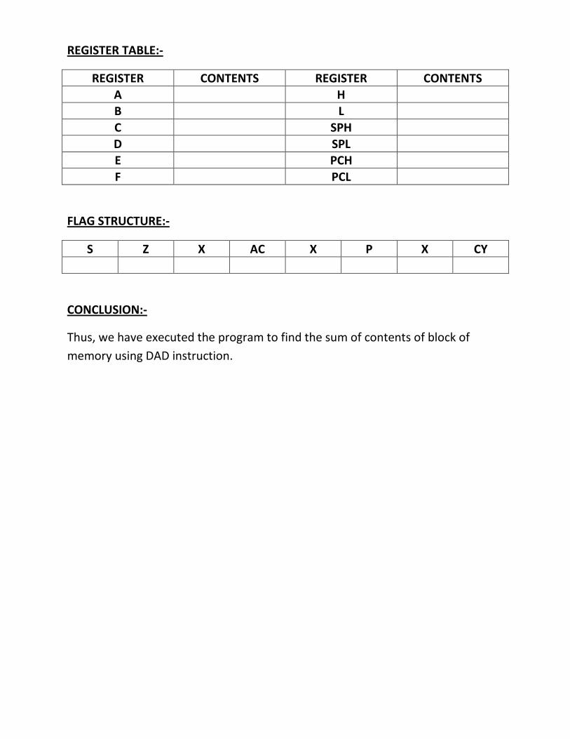
REGISTER TABLE:-
REGISTER CONTENTS REGISTER CONTENTS
A H B L
C SPH
D SPL E PCH
F PCL
FLAG STRUCTURE:-
S Z X AC X P X CY
CONCLUSION:-
Thus, we have executed the program to find the sum of contents of block of
memory using DAD instruction.
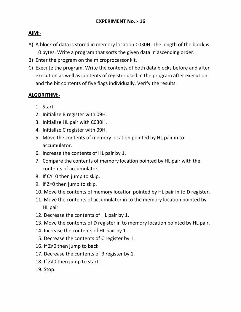
EXPERIMENT No.:- 16
AIM:-
A) A block of data is stored in memory location C030H. The length of the block is
10 bytes. Write a program that sorts the given data in ascending order.
B) Enter the program on the microprocessor kit.
C) Execute the program. Write the contents of both data blocks before and after
execution as well as contents of register used in the program after execution
and the bit contents of five flags individually. Verify the results.
ALGORITHM:-
1. Start.
2. Initialize B register with 09H.
3. Initialize HL pair with C030H.
4. Initialize C register with 09H.
5. Move the contents of memory location pointed by HL pair in to
accumulator.
6. Increase the contents of HL pair by 1.
7. Compare the contents of memory location pointed by HL pair with the
contents of accumulator.
8. If CY=0 then jump to skip.
9. If Z=0 then jump to skip.
10. Move the contents of memory location pointed by HL pair in to D register.
11. Move the contents of accumulator in to the memory location pointed by
HL pair.
12. Decrease the contents of HL pair by 1.
13. Move the contents of D register in to memory location pointed by HL pair.
14. Increase the contents of HL pair by 1.
15. Decrease the contents of C register by 1.
16. If Z≠0 then jump to back.
17. Decrease the contents of B register by 1.
18. If Z≠0 then jump to start.
19. Stop.
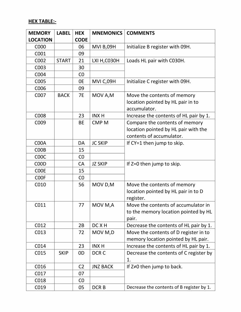
HEX TABLE:-
MEMORY LOCATION
LABEL HEX CODE
MNEMONICS COMMENTS
C000 06 MVI B,09H Initialize B register with 09H.
C001 09 C002 START 21 LXI H,C030H Loads HL pair with C030H.
C003 30
C004 C0 C005 0E MVI C,09H Initialize C register with 09H.
C006 09 C007 BACK 7E MOV A,M Move the contents of memory
location pointed by HL pair in to accumulator.
C008 23 INX H Increase the contents of HL pair by 1. C009 BE CMP M Compare the contents of memory
location pointed by HL pair with the contents of accumulator.
C00A DA JC SKIP If CY=1 then jump to skip. C00B 15
C00C C0
C00D CA JZ SKIP If Z=0 then jump to skip. C00E 15
C00F C0 C010 56 MOV D,M Move the contents of memory
location pointed by HL pair in to D register.
C011 77 MOV M,A Move the contents of accumulator in to the memory location pointed by HL pair.
C012 2B DC X H Decrease the contents of HL pair by 1.
C013 72 MOV M,D Move the contents of D register in to memory location pointed by HL pair.
C014 23 INX H Increase the contents of HL pair by 1. C015 SKIP 0D DCR C Decrease the contents of C register by
1. C016 C2 JNZ BACK If Z≠0 then jump to back.
C017 07 C018 C0
C019 05 DCR B Decrease the contents of B register by 1.
C01A C2 JNZ START If Z≠0 then jump to start.
C01B 02 C01C C0
C01D CF RST 1 Stop.
MEMORY TABLE:-
MEMORY LOCATION
BEFORE EXECUTION
AFTER EXECUTION
C030
C031
C032 C033
C034 C035
C036
C037 C038
C039
REGISTER TABLE:-
REGISTER CONTENTS REGISTER CONTENTS A H
B L C SPH
D SPL
E PCH F PCL
FLAG STRUCTURE:-
S Z X AC X P X CY
CONCLUSION:-
Thus, we have executed the program to arrange the data inside the memory block
in ascending order.
EXPERIMENT No.:- 17
AIM:-
A) A 4 byte hex number beginning with lower order byte is stored from memory
location C030H.Write a program that checks whether the given number
considered in hex is palindrome or not. If the number is palindrome then
memory location C090H must contain 00H else FFH.
B) Enter the program on the microprocessor kit.
C) Execute the program. Write the contents of both data blocks before and after
execution as well as contents of register used in the program after execution
and the bit contents of five flags individually. Verify the results.
ALGORITHM:-
1. Start.
2. Initialize HL pair by C030H.
3. Loads accumulator with contents of C033H.
4. Rotates the contents of accumulator towards right by 1 position.
5. Rotates the contents of accumulator towards right by 1 position.
6. Rotates the contents of accumulator towards right by 1 position.
7. Rotates the contents of accumulator towards right by 1 position.
8. Compare of the contents memory location with the contents of
accumulator.
9. If Z≠0 then jump to skip.
10. Increase the contents of HL pair by 1.
11. Loads the accumulator with the contents of memory location C032H.
12. Rotates the contents of accumulator towards right by 1 position.
13. Rotates the contents of accumulator towards right by 1 position.
14. Rotates the contents of accumulator towards right by 1 position.
15. Rotates the contents of accumulator towards right by 1 position.
16. Compare of the contents memory location with the contents of
accumulator.
17. If Z≠0 then jump to skip.
18. Initialize accumulator with 00H.
19. Jump to next.
20. Initialize accumulator with FFH.
21. Store the contents of accumulator at memory location C090H.
22. Stop.
HEX TABLE:-
MEMORY LOCATION
LABEL HEX CODE
MNEMONICS COMMENTS
C000 21 LXI H,C030H Loads HL pair withC030H.
C001 30
C002 C0 C003 3A LDA C033H Loads accumulator with the
contents of memory location C033H.
C004 33 C005 C0
C006 0F RRC Rotates the contents of accumulator towards right by 1 position.
C007 0F RRC Rotates the contents of accumulator towards right by 1 position.
C008 0F RRC Rotates the contents of accumulator towards right by 1 position.
C009 0F RRC Rotates the contents of accumulator towards right by 1 position.
C00A BE CMP M Compare of the contents memory location with the contents of accumulator.
C00B C2 JNZ SKIP If Z≠0 then jump to skip.
C00C 1F C00D C0
C00E 23 INX H Increase the contents of HL pair by 1.
C00F 3A LDA C032 Loads accumulator with the contents of memory location C032H.
C010 32
C011 C0
C012 0F RRC Rotates the contents of accumulator towards right by 1 position.
C013 0F RRC Rotates the contents of
accumulator towards right by 1 position.
C014 0F RRC Rotates the contents of accumulator towards right by 1 position.
C015 0F RRC Rotates the contents of accumulator towards right by 1 position.
C016 BE CMP M Compare of the contents memory location with the contents of accumulator.
C017 C2 JNZ SKIP If Z≠0 then jump to skip.
C018 1F
C019 C0 C01A 3E MVI A,00H Initialize accumulator with 00H.
C01B 00 C01C C3 JMP NEXT Jump unconditionally to next.
C01D 21 C01E C0
C01F SKIP 3E MVI A,FFH Initialize accumulator with FFH.
C020 FF C021 NEXT 32 STA C090H Store the contents of
accumulator at memory location C090H.
C022 90 C023 C0
C024 CF RST 1 Stop.
CASE 1:-
MEMORY TABLE:-
Input
MEMORY LOCATION
BEFORE EXECUTION
AFTER EXECUTION
C030 C031
C032
C033
OUTPUT
MEMORY LOCATION
BEFORE EXECUTION
AFTER EXECUTION
C090
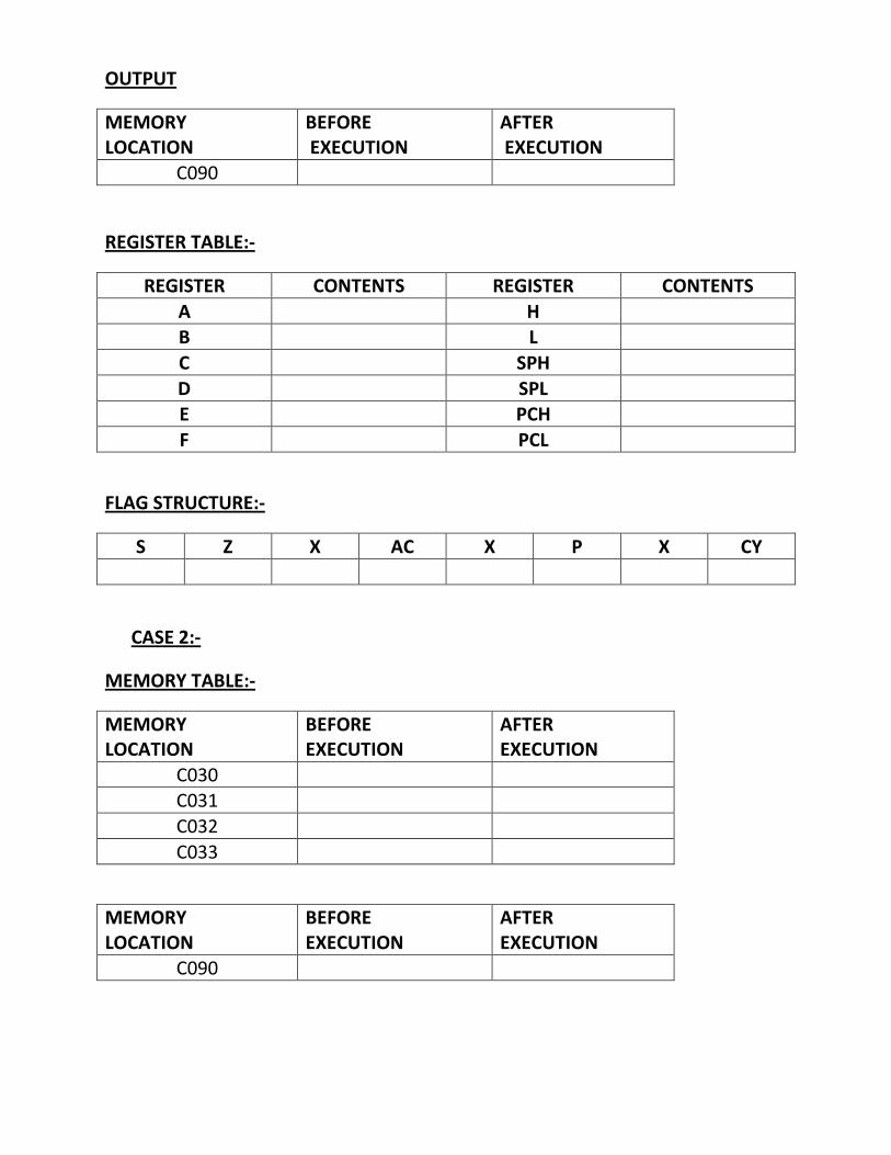
REGISTER TABLE:-
REGISTER CONTENTS REGISTER CONTENTS
A H B L
C SPH
D SPL E PCH
F PCL
FLAG STRUCTURE:-
S Z X AC X P X CY
CASE 2:-
MEMORY TABLE:-
MEMORY LOCATION
BEFORE EXECUTION
AFTER EXECUTION
C030 C031
C032
C033
MEMORY LOCATION
BEFORE EXECUTION
AFTER EXECUTION
C090
REGISTER TABLE:-
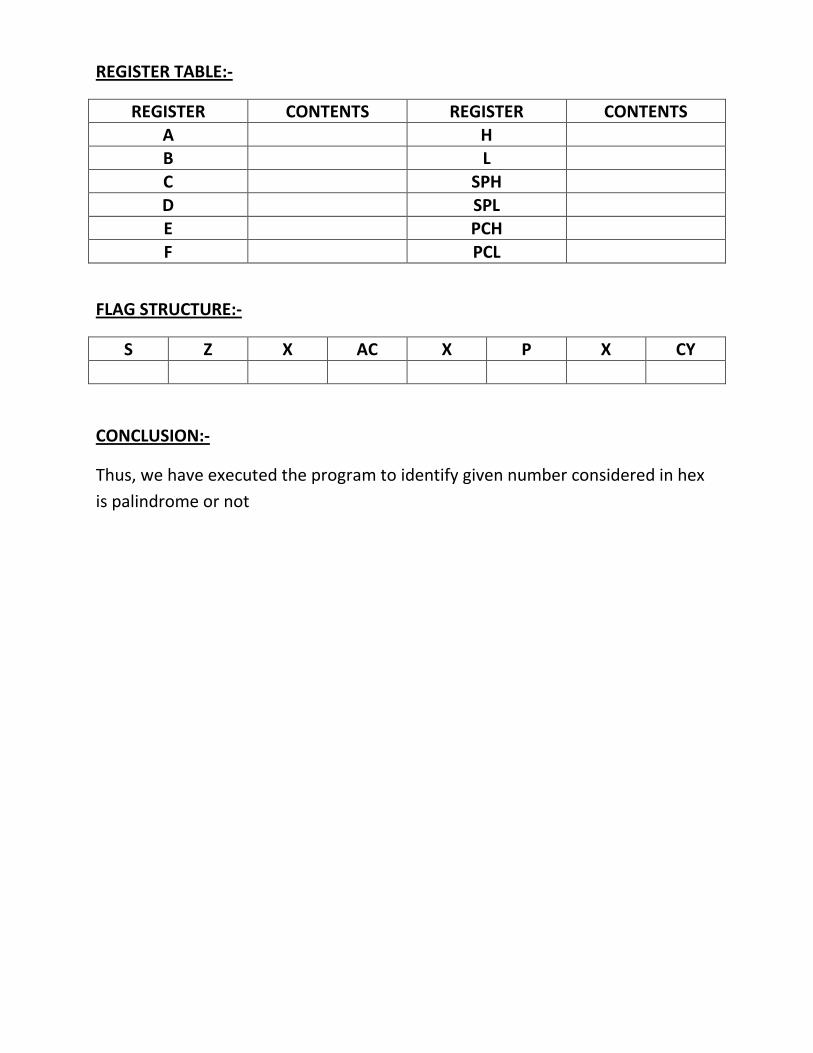
REGISTER CONTENTS REGISTER CONTENTS
A H B L
C SPH
D SPL E PCH
F PCL
FLAG STRUCTURE:-
S Z X AC X P X CY
CONCLUSION:-
Thus, we have executed the program to identify given number considered in hex
is palindrome or not
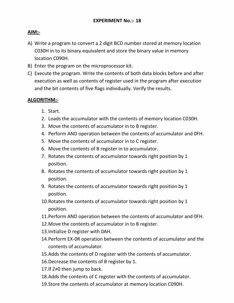
EXPERIMENT No.:- 18
AIM:-
A) Write a program to convert a 2 digit BCD number stored at memory location
C030H in to its binary equivalent and store the binary value in memory
location C090H.
B) Enter the program on the microprocessor kit.
C) Execute the program. Write the contents of both data blocks before and after
execution as well as contents of register used in the program after execution
and the bit contents of five flags individually. Verify the results.
ALGORITHM:-
1. Start.
2. Loads the accumulator with the contents of memory location C030H.
3. Move the contents of accumulator in to B register.
4. Perform AND operation between the contents of accumulator and 0FH.
5. Move the contents of accumulator in to C register.
6. Move the contents of B register in to accumulator.
7. Rotates the contents of accumulator towards right position by 1
position.
8. Rotates the contents of accumulator towards right position by 1
position.
9. Rotates the contents of accumulator towards right position by 1
position.
10. Rotates the contents of accumulator towards right position by 1
position.
11. Perform AND operation between the contents of accumulator and 0FH.
12. Move the contents of accumulator in to B register.
13. Initialize D register with 0AH.
14. Perform EX-0R operation between the contents of accumulator and the
contents of accumulator.
15. Adds the contents of D register with the contents of accumulator.
16. Decrease the contents of B register by 1.
17. If Z≠0 then jump to back.
18. Adds the contents of C register with the contents of accumulator.
19. Store the contents of accumulator at memory location C090H.
20. Stop.
HEX TABLE:-
MEMORY LOCATION
LABEL HEX CODE
MNEMONICS COMMENTS
C000 3A LDA C030H Loads the contents of memory location at C030H in to accumulator. C001 30
C002 C0 C003 47 MOV B,A Move the contents of accumulator in
to B register. C004 E6 ANI 0F Perform AND operation between the
contents of accumulator and 0FH. C005 0F C006 4F MOV C,A Move the contents of accumulator in
to C register. C007 78 MOV A,B Move the contents of B register in to
accumulator. C008 0F RRC Rotates the contents of accumulator
towards right by 1 position. C009 0F RRC Rotates the contents of accumulator
towards right by 1 position. C00A 0F RRC Rotates the contents of accumulator
towards right by 1 position. C00B 0F RRC Rotates the contents of accumulator
towards right by 1 position. C00C E6 ANI 0F Perform AND operation between the
contents of accumulator and 0FH. C00D 0F C00E 47 MOV B,A Move the contents of accumulator in
to B register. C00F 16 MVI D,0AH Initialize the D register with 0AH.
C010 0A
C011 AF XRA A Perform EX-0R operation between the contents of accumulator and the contents of accumulator.
C012 BACK 82 ADD D Adds the contents of D register with the contents of accumulator.
C013 05 DCR B Decrease the contents of B register by 1.
C014 C2 JNZ BACK If Z≠0 then jump to back.
C015 12 C016 C0
C017 81 ADD C Add the contents of C register with the contents of accumulator.
C018 32 STA C090H Store the contents of accumulator at memory location C090H. C019 90
C01A C0
C01B CF RST 1 Stop.
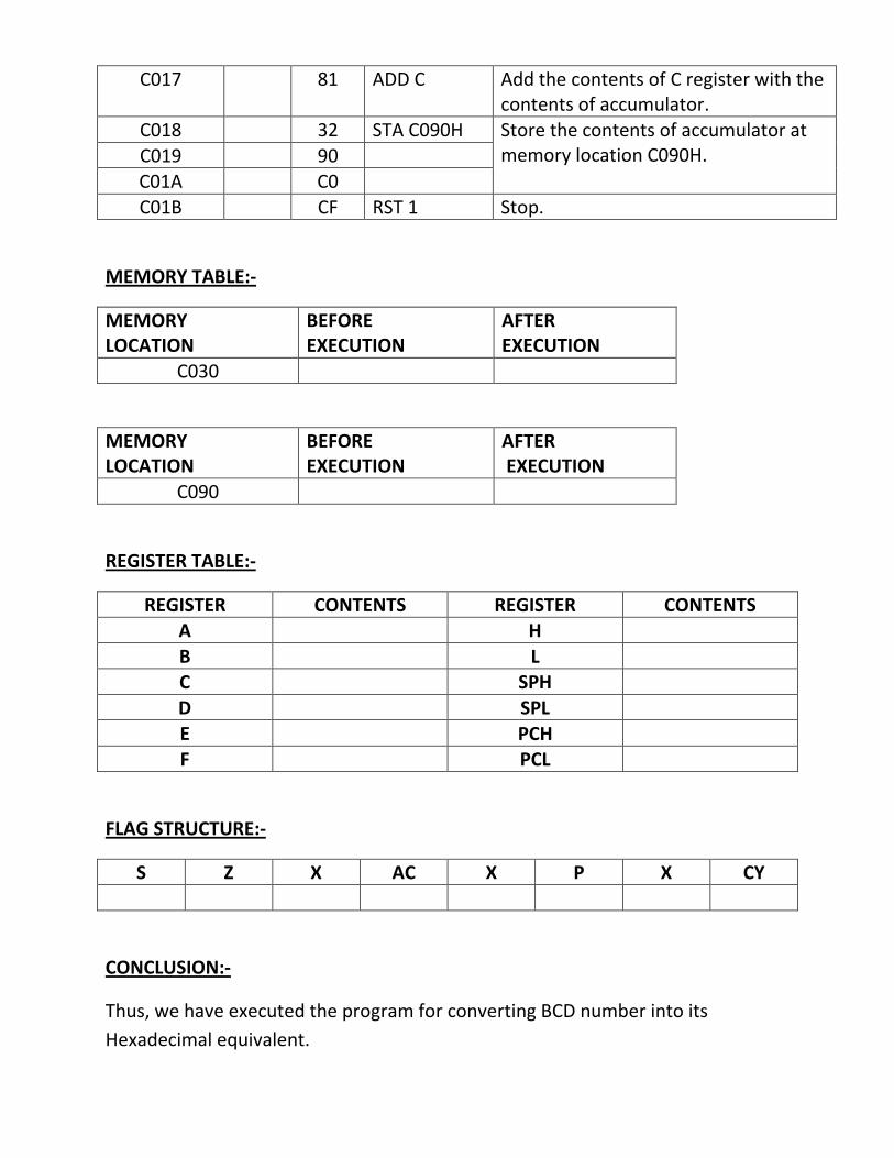
MEMORY TABLE:-
MEMORY LOCATION
BEFORE EXECUTION
AFTER EXECUTION
C030
MEMORY LOCATION
BEFORE EXECUTION
AFTER EXECUTION
C090
REGISTER TABLE:-
REGISTER CONTENTS REGISTER CONTENTS A H
B L C SPH
D SPL
E PCH F PCL
FLAG STRUCTURE:-
S Z X AC X P X CY
CONCLUSION:-
Thus, we have executed the program for converting BCD number into its
Hexadecimal equivalent.