Embed Size (px)
Citation preview
||Jai Sri Gurudev||
ADICHUNCHANAGIRI UNIVERSITY
BGS INSTITUTE OF TECHNOLOGY
BG Nagara – 571448 (Bellur Cross)
Nagamangala Taluk, Mandya District.
LINEAR IC’s AND COMMUNICATION
LABORATORY MANUAL
18ECL48
For
IV Semester B.E.
2019-2020
DEPARTMENT OF
ELECTRONICS AND COMMUNICATION ENGINEERING
Prepared by: Approved by:
1. Mrs. KAVITHA B C, Asst. Prof
2. Mrs. NANDINI S , Asst. Prof
3. Mrs. PRAFULLA P S, Asst. Prof
Head of Department
BGS Institute of Technology LIC Lab Manual (18ECL48)
Dept. of ECE 2019/2020 Page 2
DEPARTMENT OF ELECTRONICS & COMMUNICATION
ENGINEERING
VISION:
To develop high quality engineers with technical knowledge, skills and
ethics in the area of Electronics and Communication Engineering to
meet industrial and societal needs.
MISSION:
1. To provide high quality technical education with up-to-date
infrastructure and trained human resources to deliver the curriculum
effectively in order to impart technical knowledge and skills.
2. To train the students with entrepreneurship qualities, multidisciplinary
knowledge and latest skill sets as required for industry, competitive
examinations, higher studies and research activities.
3. To mould the students into professionally-ethical and socially-
responsible engineers of high character, team spirit and leadership
qualities.
PROGRAM EDUCATIONAL OBJECTIVES (PEO’s):
After 3 to 5 years of graduation, the graduates of Electronics and
Communication Engineering will;
1. Engage in industrial, teaching or any technical profession and pursue
higher studies and research.
2. Apply the knowledge of Mathematics, Science as well as Electronics
and Communication Engineering to solve social engineering problems.
3. Understand, Analyze, Design and Create novel products and solutions.
4. Display professional and leadership qualities, communication skills,
Team spirit, multidisciplinary traits and lifelong learning aptitude.
BGS Institute of Technology LIC Lab Manual (18ECL48)
Dept. of ECE 2019/2020 Page 3
LINEAR IC’S AND COMMUNICATION LAB SYLLABUS
Course Learning Objectives:
This laboratory course enables students to
Design, Demonstrate and Analyze instrumentation amplifier, filters, DAC, adder,
differentiator and integrator circuits, using op-amp.
Design, Demonstrate and Analyze multivibrator and oscillator circuits using
Op-amp
Design, Demonstrate and Analyze analog systems for AM, FM and Mixer
operations.
Design, Demonstrate and Analyze balance modulation and frequency synthesis.
Demonstrate and Analyze pulse sampling and flat top sampling.
Laboratory Experiments
1. Design an instrumentation amplifier of a differential mode gain of ‗A‘ using three
amplifiers.
2. Design of RC Phase shift and Wien‘s bridge oscillators using Op-amp.
3. Design active second order Butterworth low pass and high pass filters.
4. Design 4 bit R – 2R Op-Amp Digital to Analog Converter (i) using 4 bit binary input
from toggle switches and (ii) by generating digital inputs using mod-16 counter.
5. Design Adder, Integrator and Differentiator using Op-Amp.
6. Design of Monostable and Astable Multivibrator using 555 Timer.
7. Demonstrate Pulse sampling, flat top sampling and reconstruction.
8. Amplitude modulation using transistor/FET (Generation and detection).
9. Frequency modulation using IC 8038/2206 and demodulation.
10. Design BJT/FET Mixer.
BGS Institute of Technology LIC Lab Manual (18ECL48)
Dept. of ECE 2019/2020 Page 4
11. DSBSC generation using Balance Modulator IC 1496/1596.
12. Frequency synthesis using PLL.
Beyond Syllabus:
1. Half wave precision rectifier
BGS Institute of Technology LIC Lab Manual (18ECL48)
Dept. of ECE 2019/2020 Page 5
Course Outcomes:
On the completion of this laboratory course, the students will be able to:
Analyze the working of differential amplifier, filters and calculate cut off
frequency and roll off of filters and design oscillators for any frequency.
Generate R-2R DAC and also staircase wave using mod-16 counter, use adder
and integrator and differentiator for suitable applications.
Demonstrate the working of 555 timer and its applications and also can be able
to generate amplitude modulation, frequency modulation and pulse amplitude
modulation.
Gain hands on experience in DSBSC generation, Mixer and PLL working.
BGS Institute of Technology LIC Lab Manual (18ECL48)
Dept. of ECE 2019/2020 Page 6
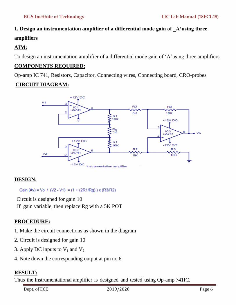
1. Design an instrumentation amplifier of a differential mode gain of ‗A‘using three
amplifiers
AIM:
To design an instrumentation amplifier of a differential mode gain of ‘A’using three amplifiers
COMPONENTS REQUIRED:
Op-amp IC 741, Resistors, Capacitor, Connecting wires, Connecting board, CRO-probes
CIRCUIT DIAGRAM:
DESIGN:
Circuit is designed for gain 10
If gain variable, then replace Rg with a 5K POT
PROCEDURE:
1. Make the circuit connections as shown in the diagram
2. Circuit is designed for gain 10
3. Apply DC inputs to V1 and V2
4. Note down the corresponding output at pin no.6
RESULT:
Thus the Instrumentational amplifier is designed and tested using Op-amp 741IC.
BGS Institute of Technology LIC Lab Manual (18ECL48)
Dept. of ECE 2019/2020 Page 7
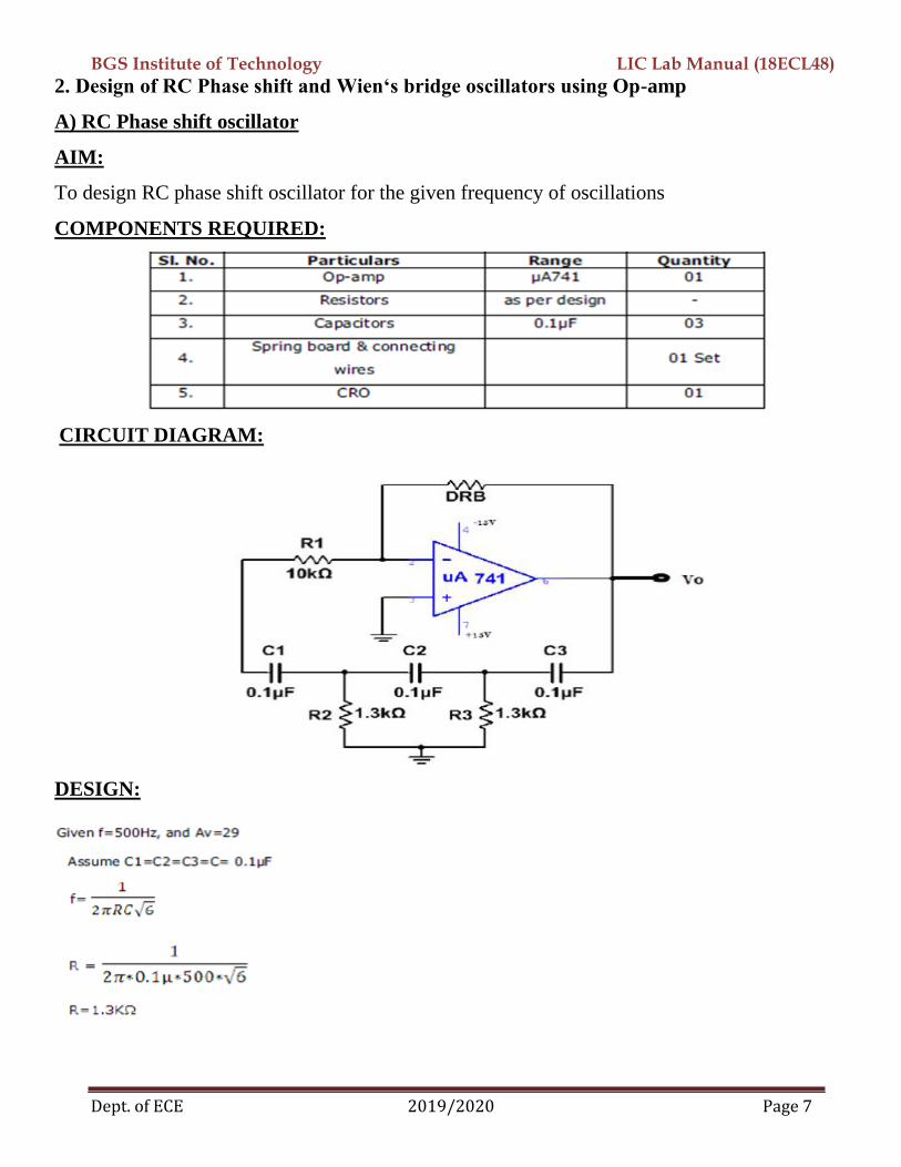
2. Design of RC Phase shift and Wien‘s bridge oscillators using Op-amp
A) RC Phase shift oscillator
AIM:
To design RC phase shift oscillator for the given frequency of oscillations
COMPONENTS REQUIRED:
CIRCUIT DIAGRAM:
DESIGN:
BGS Institute of Technology LIC Lab Manual (18ECL48)
Dept. of ECE 2019/2020 Page 8
PROCEDURE:
1. Connect the circuit as per the circuit diagram
2. Switch ON the Dual power supply & connect the CRO probe at pin no-6 of an op-amp.
3. Adjust the feedback resistor to get the oscillations. Provided that amplifier gain should meet
29
4. Observe the sine wave as output using CRO & measure the frequency.
5. Verify the frequency with the designed value
WAVEFORM:
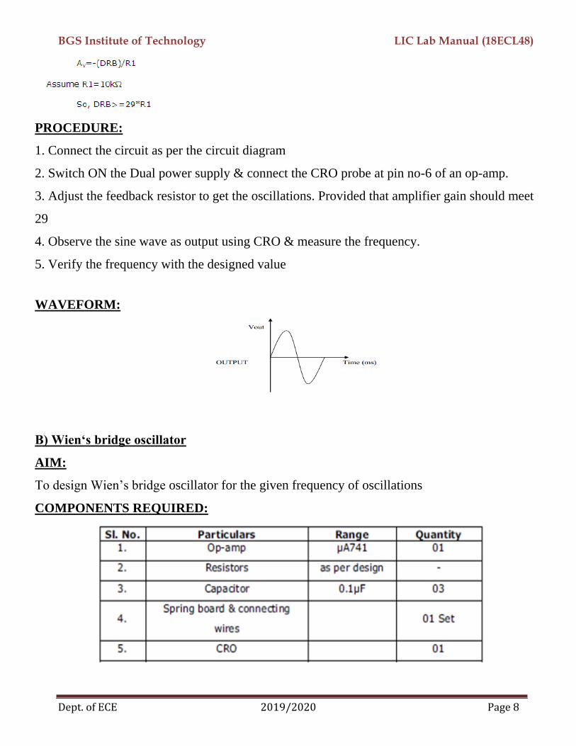
B) Wien‘s bridge oscillator
AIM:
To design Wien’s bridge oscillator for the given frequency of oscillations
COMPONENTS REQUIRED:
BGS Institute of Technology LIC Lab Manual (18ECL48)
Dept. of ECE 2019/2020 Page 9
CIRCUIT DIAGRAM:
DESIGN:
Given f=1KHz
Assume C1=C2=C=0.1µF
PROCEDURE:
1. Connect the circuit as per the circuit diagram
2. Switch ON the Dual power supply & connect the CRO probe at pin no-6 of an op-amp.
3. Adjust the feedback resistor to get the oscillations. Provided that amplifier gain should meet 3
4. Observe the sine wave as output using CRO & measure the frequency.
5. Verify the frequency with the designed value
BGS Institute of Technology LIC Lab Manual (18ECL48)
Dept. of ECE 2019/2020 Page 10
WAVEFORM:
RESULT:
Thus RC Phase Shift and Wien Bridge Oscillator were designed and tested using op-amp IC 741.
BGS Institute of Technology LIC Lab Manual (18ECL48)
Dept. of ECE 2019/2020 Page 11
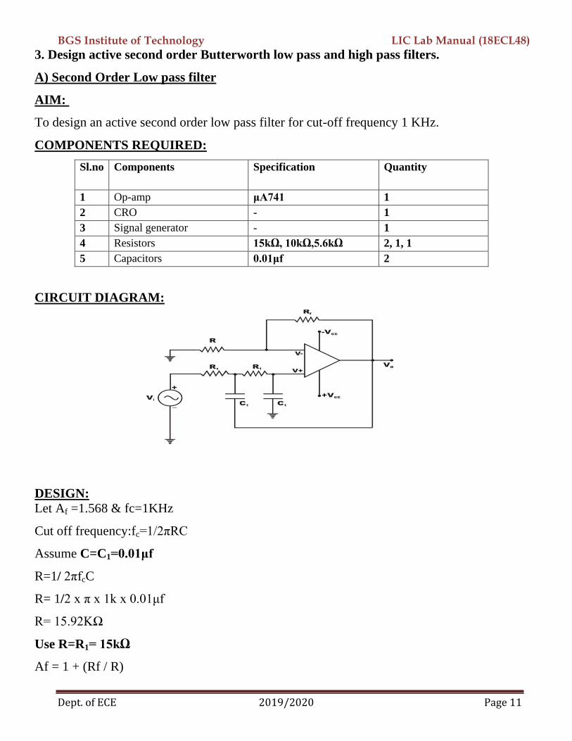
3. Design active second order Butterworth low pass and high pass filters.
A) Second Order Low pass filter
AIM:
To design an active second order low pass filter for cut-off frequency 1 KHz.
COMPONENTS REQUIRED:
Sl.no Components Specification Quantity
1 Op-amp μA741 1
2 CRO - 1
3 Signal generator - 1
4 Resistors 15kΩ, 10kΩ,5.6kΩ 2, 1, 1
5 Capacitors 0.01μf 2
CIRCUIT DIAGRAM:
DESIGN:
Let Af =1.568 & fc=1KHz
Cut off frequency:fc=1/2πRC
Assume C=C1=0.01μf
R=1/ 2πfcC
R= 1/2 x π x 1k x 0.01μf
R= 15.92KΩ
Use R=R1= 15kΩ
Af = 1 + (Rf / R)
BGS Institute of Technology LIC Lab Manual (18ECL48)
Dept. of ECE 2019/2020 Page 12
1.568-1 = Rf / R
Rf =5.6 KΩ when R=10KΩ
PROCEDURE:
1. Circuit connections are made as shown in the fig.
2. Input voltage is kept constant at 2V
3. The input frequency is varied from 100Hz to 50KHz.
4. At each step corresponding output is measured.
5. The gain in dB is calculated by using the formula Af=20 log vo/vi
6. The graph of gain v/s frequency is plotted on the graph sheet.
7. The higher cut-off frequency, roll-off rate are calculated and compared with theoretical
values.
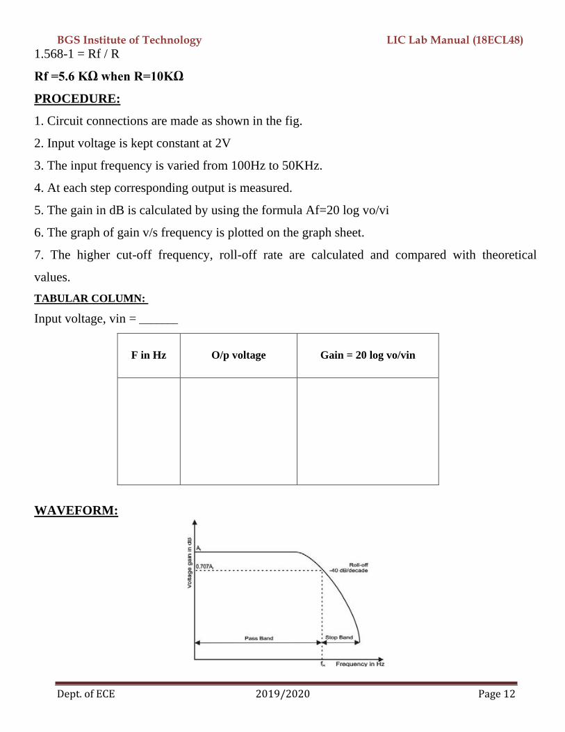
TABULAR COLUMN:
Input voltage, vin = _______
F in Hz O/p voltage
Gain = 20 log vo/vin
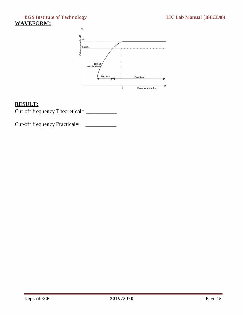
WAVEFORM:
BGS Institute of Technology LIC Lab Manual (18ECL48)
Dept. of ECE 2019/2020 Page 13
RESULT:
Cut-off frequency Theoretical= ___________
Cut-off frequency Practical= ___________
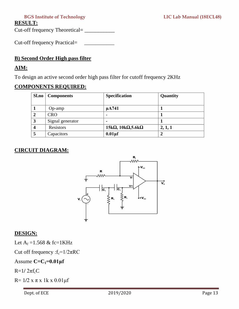
B) Second Order High pass filter
AIM:
To design an active second order high pass filter for cutoff frequency 2KHz
COMPONENTS REQUIRED:
Sl.no Components Specification Quantity
1 Op-amp μA741 1
2 CRO - 1
3 Signal generator - 1
4 Resistors 15kΩ, 10kΩ,5.6kΩ 2, 1, 1
5 Capacitors 0.01μf 2
CIRCUIT DIAGRAM:
DESIGN:
Let Af =1.568 & fc=1KHz
Cut off frequency :fc=1/2πRC
Assume C=C1=0.01μf
R=1/ 2πfcC
R= 1/2 x π x 1k x 0.01μf
BGS Institute of Technology LIC Lab Manual (18ECL48)
Dept. of ECE 2019/2020 Page 14
R= 15.92KΩ
Use R=R1= 15kΩ
Af = 1 + (Rf / R)
1.568-1 = Rf / R
Rf =5.6 KΩ when R=10KΩ
PROCEDURE:
1. Circuit connections are made as shown in the fig.
2. Input voltage is kept constant at 2V
3. The input frequency is varied from 100Hz to 50KHz
4. At each step corresponding output is measured.
5. The gain in dB is calculated by using the formula Af=20 log vo/vi
6. The graph of gain v/s frequency is plotted on the graph sheet.
7. The higher cut-off frequency, roll-off rate are calculated and compared with theoretical
values.
TABULAR COLUMN:
Input voltage, vin = _______
F in Hz O/p voltage
Gain = 20 log vo/vin
BGS Institute of Technology LIC Lab Manual (18ECL48)
Dept. of ECE 2019/2020 Page 15
WAVEFORM:
RESULT:
Cut-off frequency Theoretical= ___________
Cut-off frequency Practical= ___________
BGS Institute of Technology LIC Lab Manual (18ECL48)
Dept. of ECE 2019/2020 Page 16
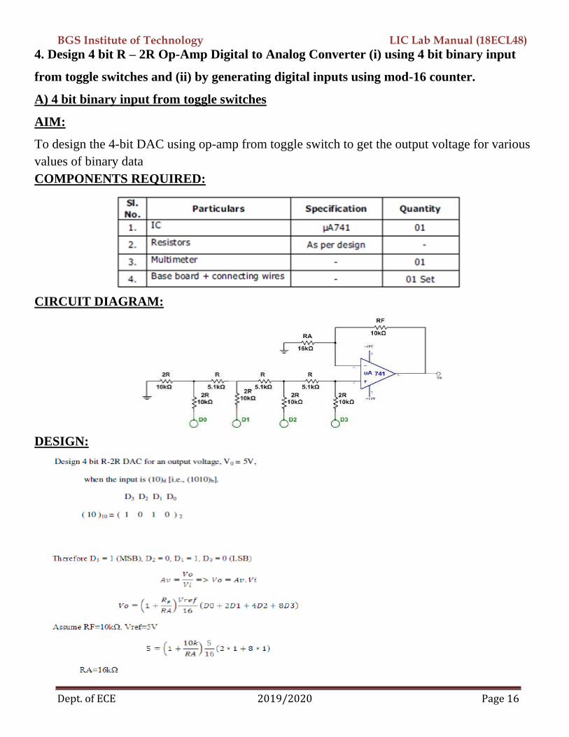
4. Design 4 bit R – 2R Op-Amp Digital to Analog Converter (i) using 4 bit binary input
from toggle switches and (ii) by generating digital inputs using mod-16 counter.
A) 4 bit binary input from toggle switches
AIM:
To design the 4-bit DAC using op-amp from toggle switch to get the output voltage for various
values of binary data
COMPONENTS REQUIRED:
CIRCUIT DIAGRAM:
DESIGN:
BGS Institute of Technology LIC Lab Manual (18ECL48)
Dept. of ECE 2019/2020 Page 17
PROCEDURE:
1. Make the connection as showm in the circuit digram
2. Digital input data is given at D3,D2,D1,D0 & corresponding analog output voltage V0 is measured
using voltmeter
3. Tabulate the readings & plot the graph of Vin V/S V0
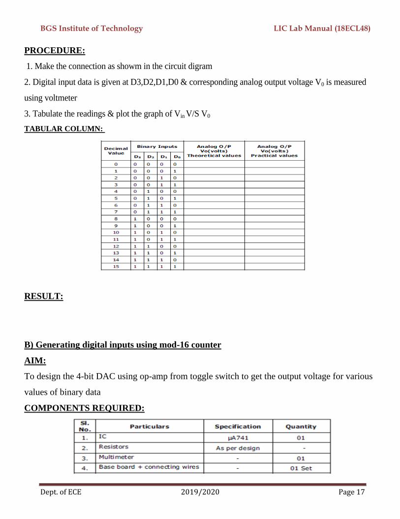
TABULAR COLUMN:
RESULT:
B) Generating digital inputs using mod-16 counter
AIM:
To design the 4-bit DAC using op-amp from toggle switch to get the output voltage for various
values of binary data
COMPONENTS REQUIRED:
BGS Institute of Technology LIC Lab Manual (18ECL48)
Dept. of ECE 2019/2020 Page 18
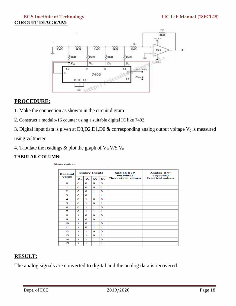
CIRCUIT DIAGRAM:
PROCEDURE:
1. Make the connection as showm in the circuit digram
2. Construct a modulo-16 counter using a suitable digital IC like 7493.
3. Digital input data is given at D3,D2,D1,D0 & corresponding analog output voltage V0 is measured
using voltmeter
4. Tabulate the readings & plot the graph of Vin V/S V0
TABULAR COLUMN:
RESULT:
The analog signals are converted to digital and the analog data is recovered
BGS Institute of Technology LIC Lab Manual (18ECL48)
Dept. of ECE 2019/2020 Page 19
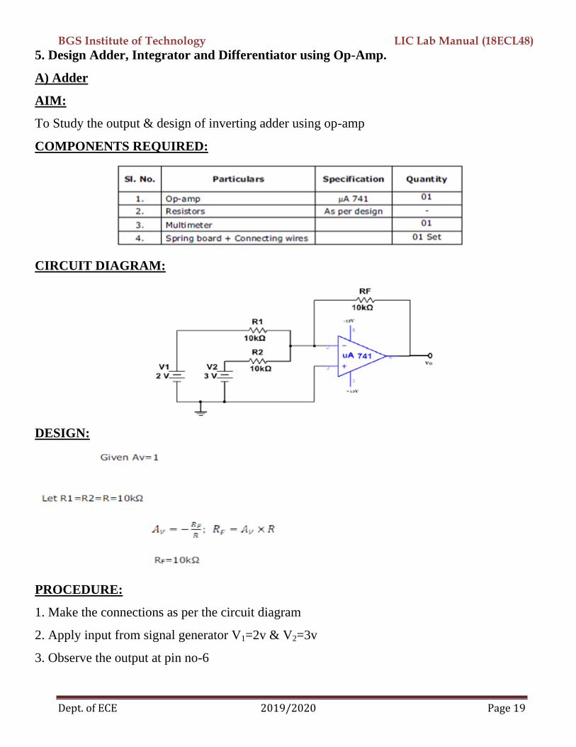
5. Design Adder, Integrator and Differentiator using Op-Amp.
A) Adder
AIM:
To Study the output & design of inverting adder using op-amp
COMPONENTS REQUIRED:
CIRCUIT DIAGRAM:
DESIGN:
PROCEDURE:
1. Make the connections as per the circuit diagram
2. Apply input from signal generator V1=2v & V2=3v
3. Observe the output at pin no-6
BGS Institute of Technology LIC Lab Manual (18ECL48)
Dept. of ECE 2019/2020 Page 20
TABULAR COLUMN:
RESULT:
Thus an Adder using op-amp are designed and their performance was successfully tested using op-amp IC 741.
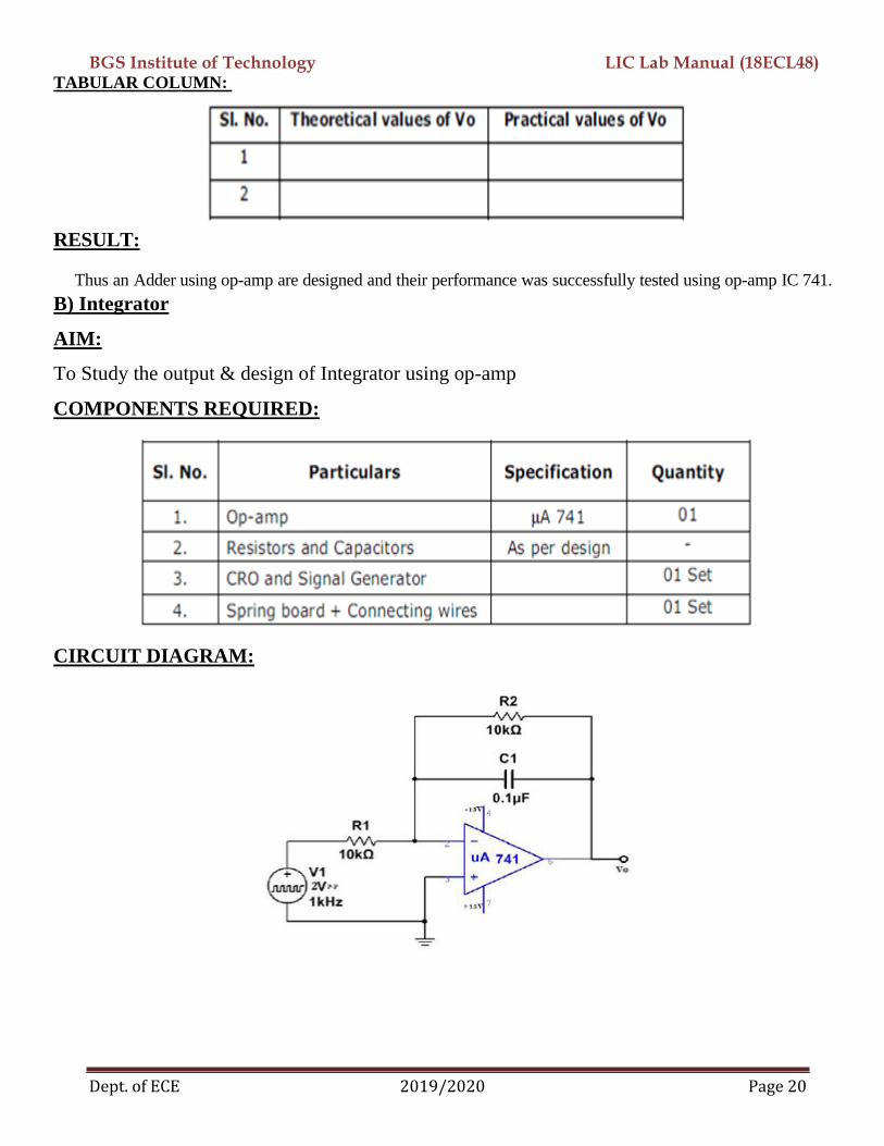
B) Integrator
AIM:
To Study the output & design of Integrator using op-amp
COMPONENTS REQUIRED:
CIRCUIT DIAGRAM:
BGS Institute of Technology LIC Lab Manual (18ECL48)
Dept. of ECE 2019/2020 Page 21
DESIGN:
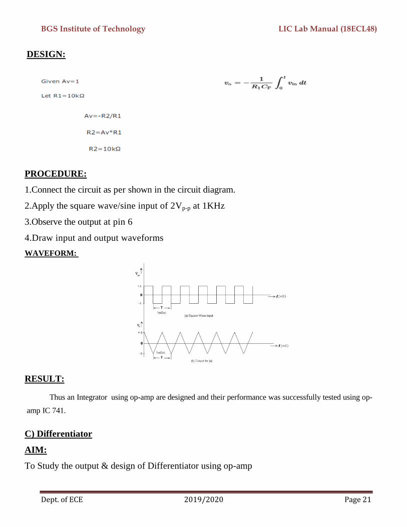
PROCEDURE:
1.Connect the circuit as per shown in the circuit diagram.
2.Apply the square wave/sine input of 2Vp-p at 1KHz
3.Observe the output at pin 6
4.Draw input and output waveforms
WAVEFORM:
RESULT:
Thus an Integrator using op-amp are designed and their performance was successfully tested using op-
amp IC 741.
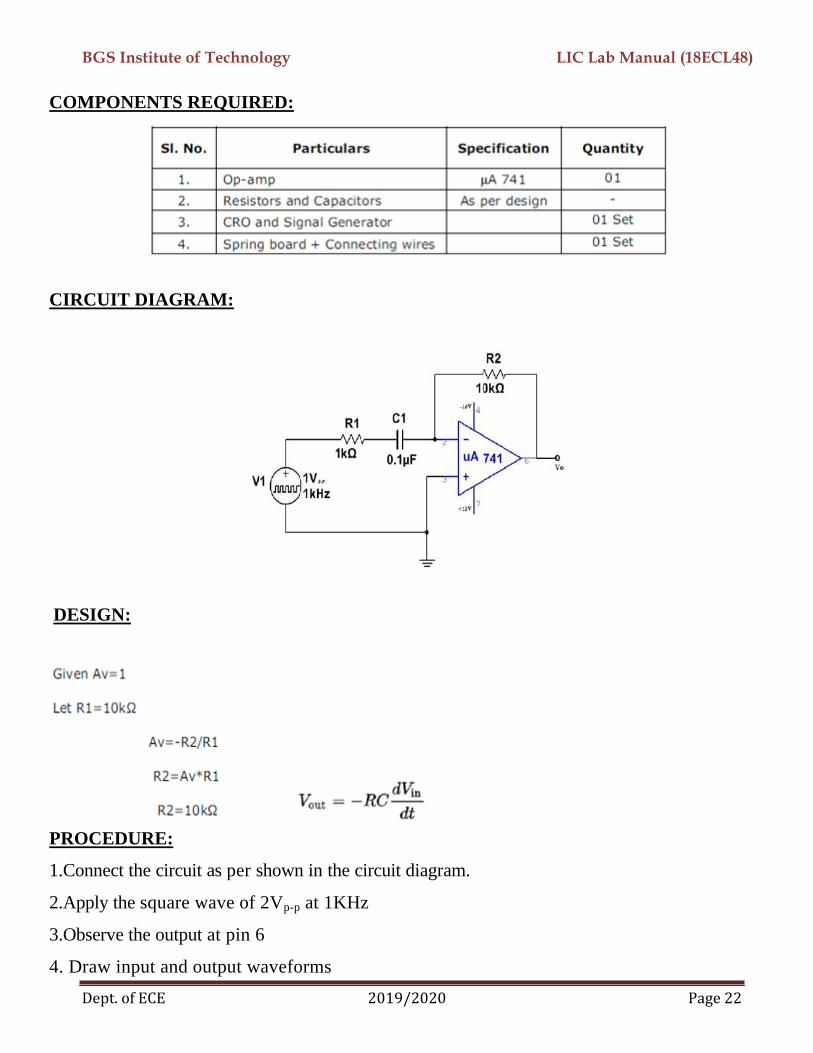
C) Differentiator
AIM:
To Study the output & design of Differentiator using op-amp
BGS Institute of Technology LIC Lab Manual (18ECL48)
Dept. of ECE 2019/2020 Page 22
COMPONENTS REQUIRED:
CIRCUIT DIAGRAM:
DESIGN:
PROCEDURE:
1.Connect the circuit as per shown in the circuit diagram.
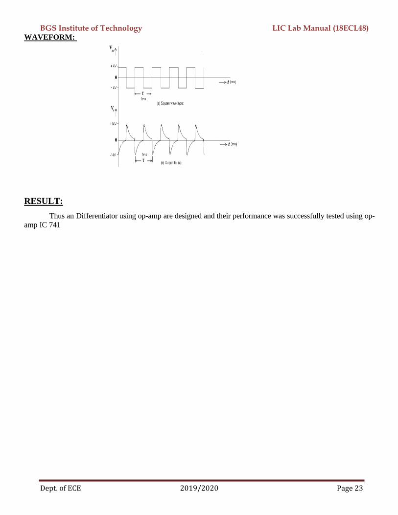
2.Apply the square wave of 2Vp-p at 1KHz
3.Observe the output at pin 6
4. Draw input and output waveforms
BGS Institute of Technology LIC Lab Manual (18ECL48)
Dept. of ECE 2019/2020 Page 23
WAVEFORM:
RESULT:
Thus an Differentiator using op-amp are designed and their performance was successfully tested using op-
amp IC 741
BGS Institute of Technology LIC Lab Manual (18ECL48)
Dept. of ECE 2019/2020 Page 24
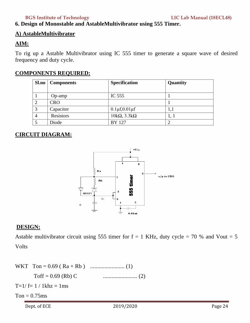
6. Design of Monostable and AstableMultivibrator using 555 Timer.
A) AstableMultivibrator
AIM:
To rig up a Astable Multivibrator using IC 555 timer to generate a square wave of desired
frequency and duty cycle.
COMPONENTS REQUIRED:
Sl.no Components Specification Quantity
1 Op-amp IC 555 1
2 CRO 1
3 Capacitor 0.1μf,0.01μf 1,1
4 Resistors 10kΩ, 3.3kΩ 1, 1
5 Diode BY 127 2
CIRCUIT DIAGRAM:
DESIGN:
Astable multivibrator circuit using 555 timer for f = 1 KHz, duty cycle = 70 % and Vout = 5
Volts
WKT Ton = 0.69 ( Ra + Rb ) ........................ (1)
Toff = 0.69 (Rb) C ........................ (2)
T=1/ f= 1 / 1khz = 1ms
Ton = 0.75ms
BGS Institute of Technology LIC Lab Manual (18ECL48)
Dept. of ECE 2019/2020 Page 25
Toff = 0.25ms
Choose c=0.1μf
From equation (2)
0.25m=0.69(Rb)0.1μ
Rb=3.62kΩ use Rb=3.3kΩ
From equation (1)
0.75=0.69(Ra+3.3k)
Ra=7.66kΩ use Ra=10kΩ
PROCEDURE:
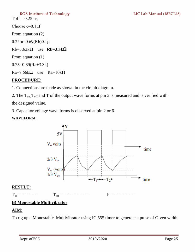
1. Connections are made as shown in the circuit diagram.
2. The Ton, Toff and T of the output wave forms at pin 3 is measured and is verified with
the designed value.
3. Capacitor voltage wave forms is observed at pin 2 or 6.
WAVEFORM:
RESULT:
Ton = ----------- Toff = ----------------- F= ---------------
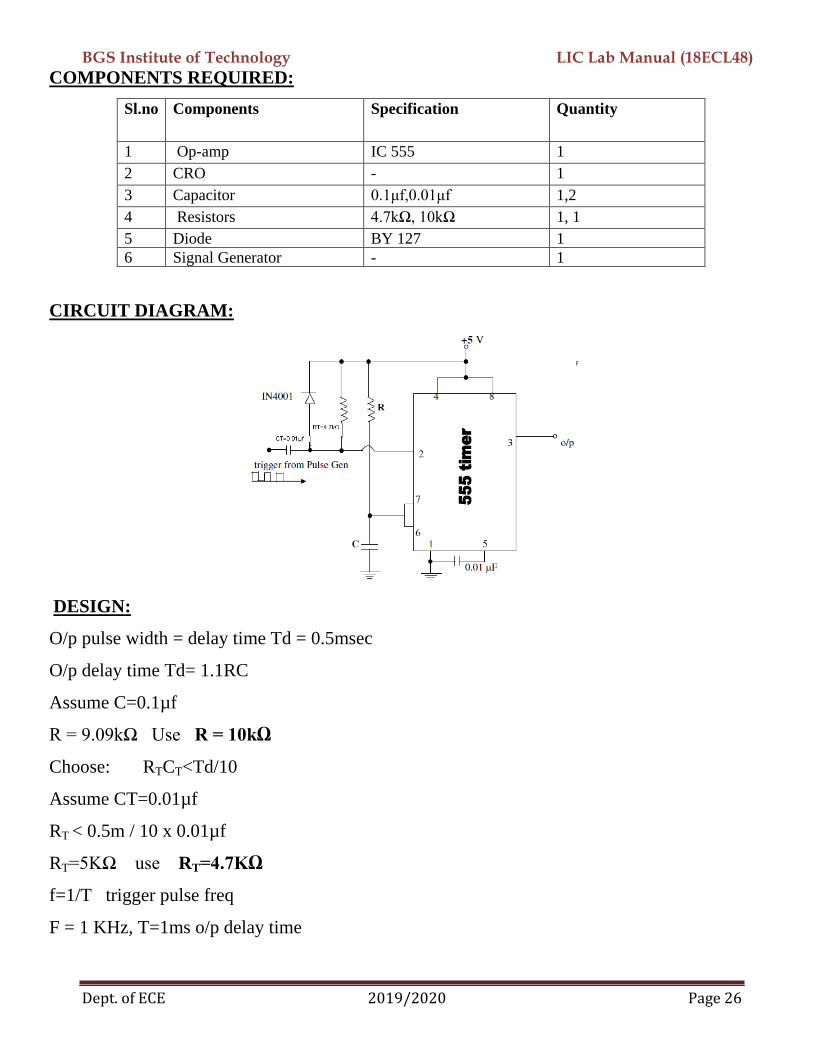
B) Monostable Multivibrator
AIM:
To rig up a Monostable Multivibrator using IC 555 timer to generate a pulse of Given width
BGS Institute of Technology LIC Lab Manual (18ECL48)
Dept. of ECE 2019/2020 Page 26
COMPONENTS REQUIRED:
Sl.no Components Specification Quantity
1 Op-amp IC 555 1
2 CRO - 1
3 Capacitor 0.1μf,0.01μf 1,2
4 Resistors 4.7kΩ, 10kΩ 1, 1
5 Diode BY 127 1
6 Signal Generator - 1
CIRCUIT DIAGRAM:
DESIGN:
O/p pulse width = delay time Td = 0.5msec
O/p delay time Td= 1.1RC
Assume C=0.1µf
R = 9.09kΩ Use R = 10kΩ
Choose: RTCT<Td/10
Assume CT=0.01µf
RT < 0.5m / 10 x 0.01µf
RT=5KΩ use RT=4.7KΩ
f=1/T trigger pulse freq
F = 1 KHz, T=1ms o/p delay time
BGS Institute of Technology LIC Lab Manual (18ECL48)
Dept. of ECE 2019/2020 Page 27
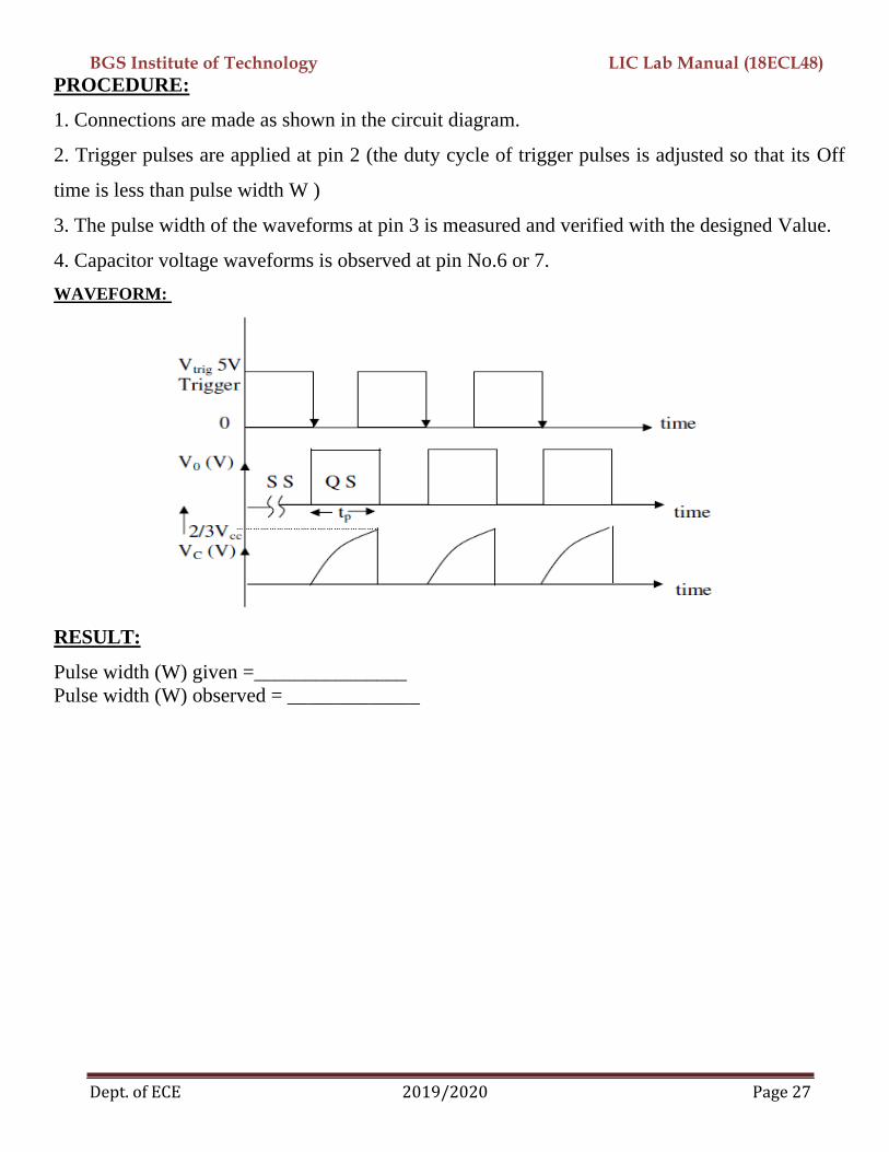
PROCEDURE:
1. Connections are made as shown in the circuit diagram.
2. Trigger pulses are applied at pin 2 (the duty cycle of trigger pulses is adjusted so that its Off
time is less than pulse width W )
3. The pulse width of the waveforms at pin 3 is measured and verified with the designed Value.
4. Capacitor voltage waveforms is observed at pin No.6 or 7.
WAVEFORM:
RESULT:
Pulse width (W) given =_______________
Pulse width (W) observed = _____________
BGS Institute of Technology LIC Lab Manual (18ECL48)
Dept. of ECE 2019/2020 Page 28
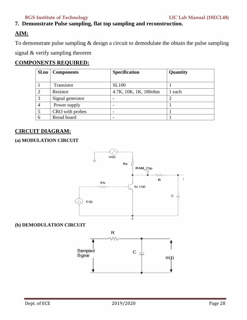
7. Demonstrate Pulse sampling, flat top sampling and reconstruction.
AIM:
To demonstrate pulse sampling & design a circuit to demodulate the obtain the pulse sampling
signal & verify sampling theorem
COMPONENTS REQUIRED:
Sl.no Components Specification Quantity
1 Transistor SL100 1
2 Resistor 4.7K, 10K, 1K, 180ohm 1 each
3 Signal generator - 2
4 Power supply - 1
5 CRO with probes - 1
6 Bread board - 1
CIRCUIT DIAGRAM:
(a) MODULATION CIRCUIT
(b) DEMODULATION CIRCUIT
BGS Institute of Technology LIC Lab Manual (18ECL48)
Dept. of ECE 2019/2020 Page 29
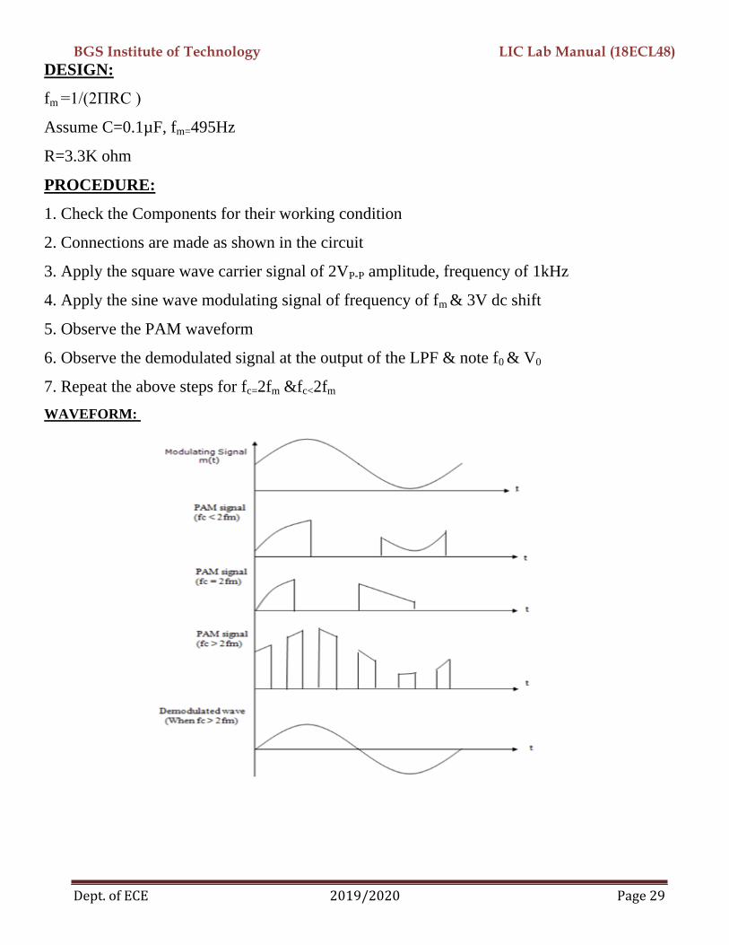
DESIGN:
fm =1/(2ΠRC )
Assume C=0.1µF, fm=495Hz
R=3.3K ohm
PROCEDURE:
1. Check the Components for their working condition
2. Connections are made as shown in the circuit
3. Apply the square wave carrier signal of 2VP-P amplitude, frequency of 1kHz
4. Apply the sine wave modulating signal of frequency of fm & 3V dc shift
5. Observe the PAM waveform
6. Observe the demodulated signal at the output of the LPF & note f0 & V0
7. Repeat the above steps for fc=2fm &fc<2fm
WAVEFORM:
BGS Institute of Technology LIC Lab Manual (18ECL48)
Dept. of ECE 2019/2020 Page 30
TABULAR COLUMN:
PAM
(v)
Emax(v) Emin(v) %µ=( Emax- Emin) /
( Emax+ Emin)x100
2
3
4
5
RESULT:
The output of pulse sampling & the demodulation circuit are verified using the waveform
BGS Institute of Technology LIC Lab Manual (18ECL48)
Dept. of ECE 2019/2020 Page 31
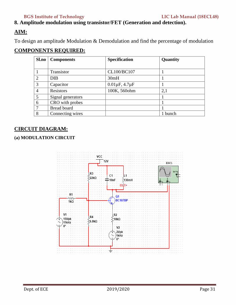
8. Amplitude modulation using transistor/FET (Generation and detection).
AIM:
To design an amplitude Modulation & Demodulation and find the percentage of modulation
COMPONENTS REQUIRED:
Sl.no Components Specification Quantity
1 Transistor CL100/BC107 1
2 DIB 30mH 1
3 Capacitor 0.01µF, 4.7µF 1
4 Resistors 100K, 560ohm 2,1
5 Signal generators 1
6 CRO with probes 1
7 Bread board 1
8 Connecting wires 1 bunch
CIRCUIT DIAGRAM:
(a) MODULATION CIRCUIT
BGS Institute of Technology LIC Lab Manual (18ECL48)
Dept. of ECE 2019/2020 Page 32
(b) DEMODULATION CIRCUIT
DESIGN:
fm =1/(2ΠRC )
Assume C=0.1µF, fm=495Hz
R=3.3K ohm
PROCEDURE:
1. Make connections as shown in figure.
2. Set the carrier frequency.
3. Set the modulating signal.
4. Keep carrier amplitude constant and vary the modulating voltage in steps and measure
5. Measure Vmax and Vmin, and calculate modulation index.
WAVEFORM:
BGS Institute of Technology LIC Lab Manual (18ECL48)
Dept. of ECE 2019/2020 Page 33
TABULAR COLUMN:
M(t)(v) Emax(v) Emin(v) %µ=( Emax- Emin) /
( Emax+ Emin)x100
2
3
4
5
RESULT:
The amplitude modulation & demodulation circuit are verified. The modulation index is also
verified
BGS Institute of Technology LIC Lab Manual (18ECL48)
Dept. of ECE 2019/2020 Page 34
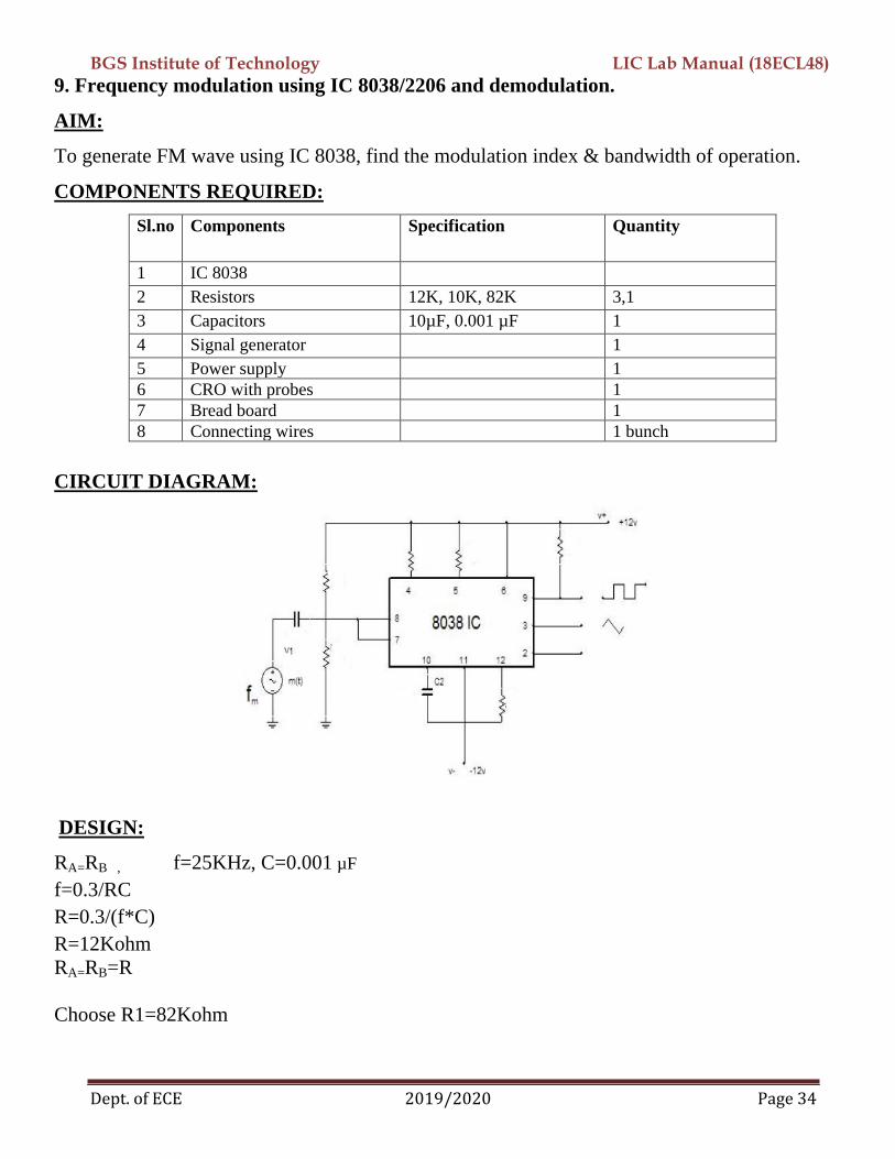
9. Frequency modulation using IC 8038/2206 and demodulation.
AIM:
To generate FM wave using IC 8038, find the modulation index & bandwidth of operation.
COMPONENTS REQUIRED:
Sl.no Components Specification Quantity
1 IC 8038
2 Resistors 12K, 10K, 82K 3,1
3 Capacitors 10µF, 0.001 µF 1
4 Signal generator 1
5 Power supply 1
6 CRO with probes 1
7 Bread board 1
8 Connecting wires 1 bunch
CIRCUIT DIAGRAM:
DESIGN:
RA=RB , f=25KHz, C=0.001 µF
f=0.3/RC
R=0.3/(f*C)
R=12Kohm
RA=RB=R
Choose R1=82Kohm
BGS Institute of Technology LIC Lab Manual (18ECL48)
Dept. of ECE 2019/2020 Page 35
PROCEDURE:
1. Check the components/ Equipments for their working condition.
2. Connections are made as shown in the circuit diagram.
3. By switching off the modulating signal m(t) note the frequency of the carrier wave at PinNo.2
of IC-8038.
4. Apply the modulating signal with suitable amplitude to get the FM signal.
5. Note the maximum (fmax) and minimum (fmin) frequency of the carrier wave in FM signal
6. Calculate the frequency deviation, modulation index and bandwidth.
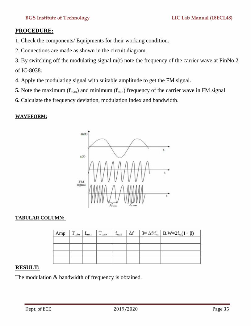
WAVEFORM:
TABULAR COLUMN:
Amp Tmin fmax Tmax fmin Δf β= Δf/fm B.W=2fm(1+ β)
RESULT:
The modulation & bandwidth of frequency is obtained.
BGS Institute of Technology LIC Lab Manual (18ECL48)
Dept. of ECE 2019/2020 Page 36
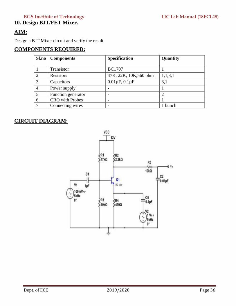
10. Design BJT/FET Mixer.
AIM:
Design a BJT Mixer circuit and verify the result
COMPONENTS REQUIRED:
Sl.no Components Specification Quantity
1 Transistor BC1707 1
2 Resistors 47K, 22K, 10K,560 ohm 1,1,3,1
3 Capacitors 0.01µF, 0.1µF 3,1
4 Power supply - 1
5 Function generator - 2
6 CRO with Probes - 1
7 Connecting wires - 1 bunch
CIRCUIT DIAGRAM:
BGS Institute of Technology LIC Lab Manual (18ECL48)
Dept. of ECE 2019/2020 Page 37
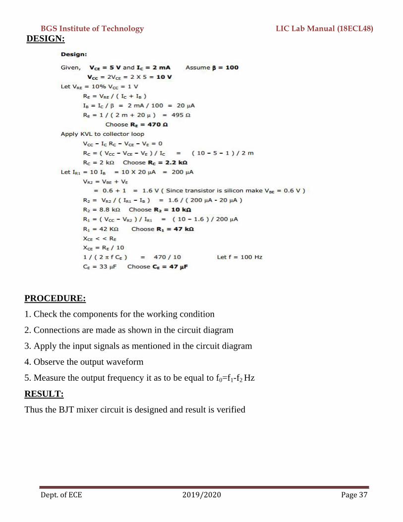
DESIGN:
PROCEDURE:
1. Check the components for the working condition
2. Connections are made as shown in the circuit diagram
3. Apply the input signals as mentioned in the circuit diagram
4. Observe the output waveform
5. Measure the output frequency it as to be equal to f0=f1-f2 Hz
RESULT:
Thus the BJT mixer circuit is designed and result is verified
BGS Institute of Technology LIC Lab Manual (18ECL48)
Dept. of ECE 2019/2020 Page 38
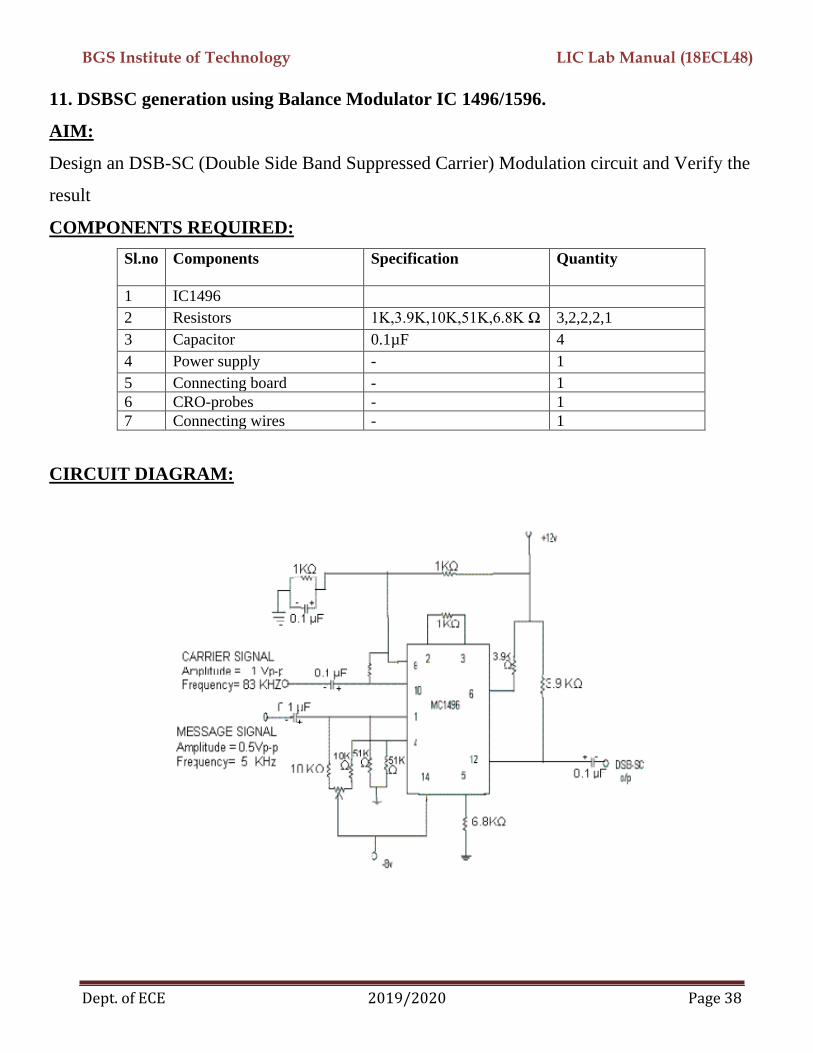
11. DSBSC generation using Balance Modulator IC 1496/1596.
AIM:
Design an DSB-SC (Double Side Band Suppressed Carrier) Modulation circuit and Verify the
result
COMPONENTS REQUIRED:
Sl.no Components Specification Quantity
1 IC1496
2 Resistors 1K,3.9K,10K,51K,6.8K Ω 3,2,2,2,1
3 Capacitor 0.1µF 4
4 Power supply - 1
5 Connecting board - 1
6 CRO-probes - 1
7 Connecting wires - 1
CIRCUIT DIAGRAM:
BGS Institute of Technology LIC Lab Manual (18ECL48)
Dept. of ECE 2019/2020 Page 39
PROCEDURE:
1. Check the components for their working condition
2. Connections are made as shown in the circuit diagram
3. Apply the carrier signal of 1Vp-p amplitude & frequency of 83KHz is applied as carrier to pin
no-10
4. Apply the message signal of 0.5Vp-p amplitude & frequency of 5KHz is given as message
signal to pin no-1
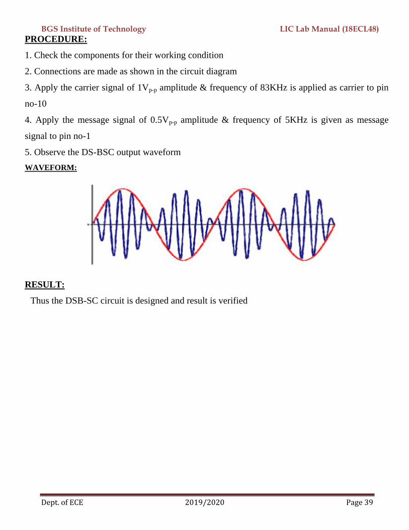
5. Observe the DS-BSC output waveform
WAVEFORM:
RESULT:
Thus the DSB-SC circuit is designed and result is verified
BGS Institute of Technology LIC Lab Manual (18ECL48)
Dept. of ECE 2019/2020 Page 40
12. Frequency synthesis using PLL.
AIM:
To conduct an experiment to study FM demodulation using 565 IC PLL
COMPONENTS REQUIRED:
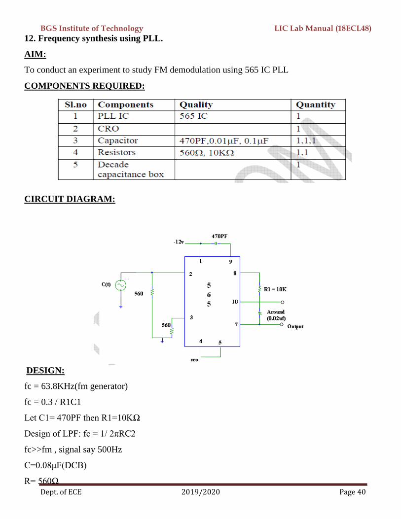
CIRCUIT DIAGRAM:
DESIGN:
fc = 63.8KHz(fm generator)
fc = 0.3 / R1C1
Let C1= 470PF then R1=10KΩ
Design of LPF: fc = 1/ 2πRC2
fc>>fm , signal say 500Hz
C=0.08μF(DCB)
R= 560Ω
BGS Institute of Technology LIC Lab Manual (18ECL48)
Dept. of ECE 2019/2020 Page 41
PROCEDURE:
1. With Pin no.4 & 5 disconnected & without FM at pin no.
2. Measure the VCO frequency at pin no.4 and make it to be 63.8 KHz by adjusting
3. Inter connect pin no.4 & 5 and apply un modulated carrier to pin no.2
4. Slightly vary the carrier frequency, VCO frequency also changes, the PLL is locked. If VCO
frequency does not change if PLL is not locked, changes input frequency or VCO frequency to
lock the PLL
5. In the same rate modulate the carrier at pin no.2 and observe demodulate signal at pinno.7 and
compare if m(t) modulation signal.
RESULT:
Frequency synthesis using PLL circuit is verified
BGS Institute of Technology LIC Lab Manual (18ECL48)
Dept. of ECE 2019/2020 Page 42
BEYOND SYLLABUS
1. Half wave precision rectifier
AIM:
To design and obtain half wave precision rectification using OP-Amp and to observe the transfer
characteristics.
COMPONENTS REQUIRED:
Sl.
no
Components Specification Quantity
1 Op-amp μA741 1
2 Resistors 10K ohm 1
3 Diode IN4007 1
4 Signal generator - 1
5 Connecting board - 1
6 CRO-probes - 1
7 CRO - 1
8 Connecting wires - 1 bunch
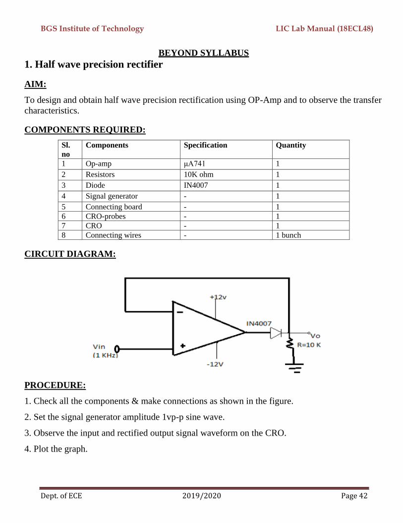
CIRCUIT DIAGRAM:
PROCEDURE:
1. Check all the components & make connections as shown in the figure.
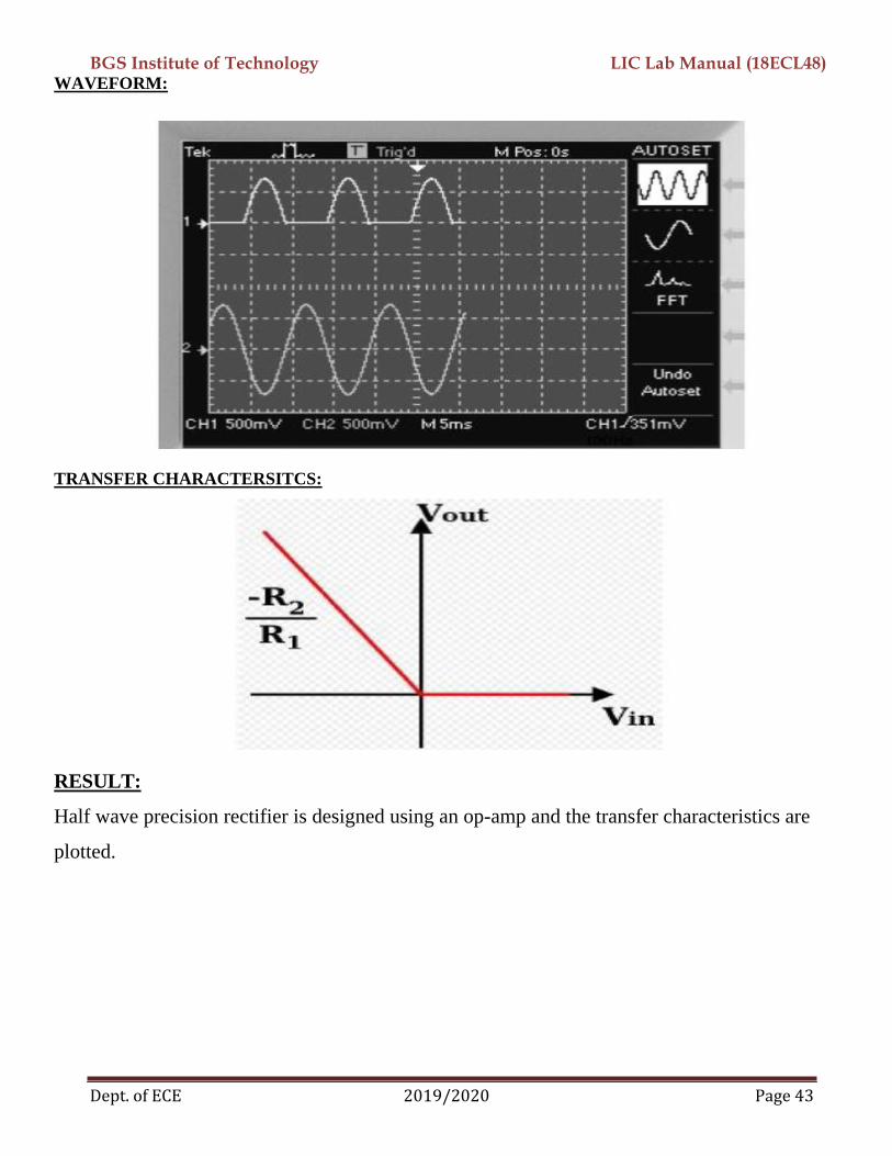
2. Set the signal generator amplitude 1vp-p sine wave.
3. Observe the input and rectified output signal waveform on the CRO.
4. Plot the graph.
BGS Institute of Technology LIC Lab Manual (18ECL48)
Dept. of ECE 2019/2020 Page 43
WAVEFORM:
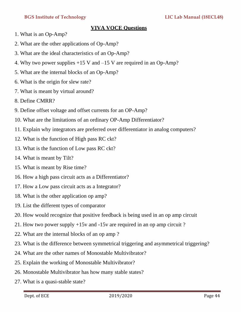
TRANSFER CHARACTERSITCS:
RESULT:
Half wave precision rectifier is designed using an op-amp and the transfer characteristics are
plotted.
BGS Institute of Technology LIC Lab Manual (18ECL48)
Dept. of ECE 2019/2020 Page 44
VIVA VOCE Questions
1. What is an Op-Amp?
2. What are the other applications of Op-Amp?
3. What are the ideal characteristics of an Op-Amp?
4. Why two power supplies +15 V and –15 V are required in an Op-Amp?
5. What are the internal blocks of an Op-Amp?
6. What is the origin for slew rate?
7. What is meant by virtual around?
8. Define CMRR?
9. Define offset voltage and offset currents for an OP-Amp?
10. What are the limitations of an ordinary OP-Amp Differentiator?
11. Explain why integrators are preferred over differentiator in analog computers?
12. What is the function of High pass RC ckt?
13. What is the function of Low pass RC ckt?
14. What is meant by Tilt?
15. What is meant by Rise time?
16. How a high pass circuit acts as a Differentiator?
17. How a Low pass circuit acts as a Integrator?
18. What is the other application op amp?
19. List the different types of comparator
20. How would recognize that positive feedback is being used in an op amp circuit
21. How two power supply +15v and -15v are required in an op amp circuit ?
22. What are the internal blocks of an op amp ?
23. What is the difference between symmetrical triggering and asymmetrical triggering?
24. What are the other names of Monostable Multivibrator?
25. Explain the working of Monostable Multivibrator?
26. Monostable Multivibrator has how many stable states?
27. What is a quasi-stable state?
BGS Institute of Technology LIC Lab Manual (18ECL48)
Dept. of ECE 2019/2020 Page 45
28. What are the applications of MonostableMultivibrator?
29. What are the initial states of a Monostable Multivibrator?
30. Which type of Triggering is used in Monostable Multivibrator?
31. What is the effect of temperature on Monostable Multivibrator?
32. Which type of feedback is present in Monostable Multivibrator?
33. Derive the expression for pulse width?
34. What is the other name of Astable Multivibrator?
35. Explain the working of Astable Multivibrator?
36. What is a quasi-stable state?
37. What are the applications of Astable Multivibrator?
38. Explain Hoe Astable Multivibrator can be used as a voltage to frequency
converter?
39. Which type of biasing present in Astable Multivibrator?
40. How Astable acts as a free running oscillator?
41. Define time constant?
42. Define UTP & LTP?
43. What is the other name of a Schmitt Trigger ckt?
44. Explain the working of Schmitt Trigger ckt?
45. What are the applications of Schmitt Trigger?
46. What is a Voltage Regulator?
47. What are the advantages of adjustable voltage regulators over the fixed voltage
regulators?
48. What is voltage reference? Why it is needed?
49. What is the function of a series pass transistor?
50. What voltage options are variables in 78XX and 79XX voltage regulators?
51. Show the standard representation of IC voltage regulator?
52. List and explain the characteristics of three terminal IC voltage regulators?
53. Explain the important parameters of 78XX regulator?
BGS Institute of Technology LIC Lab Manual (18ECL48)
Dept. of ECE 2019/2020 Page 46
54. Explain the protections used in 78XX?
55. What are the Limitations of three terminal voltage regulators?
56. Define Duty Cycle?
57. What are the other applications of 555 timer?
58. Draw the internal circuit diagram of 555 timer?
59. Explain the operation of 555 timer?
60. Explain the function of reset?
61. Derive the expression for time delay of monostable multivibrator?
62. Discuss the applications of timer in monostable multivibrator?
63. Give methods for obtaining symmetrical square wave?
64. what are the modes of operation of a 555 timer?
65. Discuss the operation of a FSK generator using timer?
BGS Institute of Technology LIC Lab Manual (18ECL48)
Dept. of ECE 2019/2020 Page 47