Embed Size (px)
Citation preview

Line Rectification and Capacitor Input Filters For Direct-off-Line Switchmode
Power Supplies

Overview
• Switchmode Supplies vs. Linear Supplies
• Characteristics of typical Direct-off-line Circuit for Switchmode Supplies
• Characteristics of Switchmode Supplies
• Simulation
• Calculations
• Applications
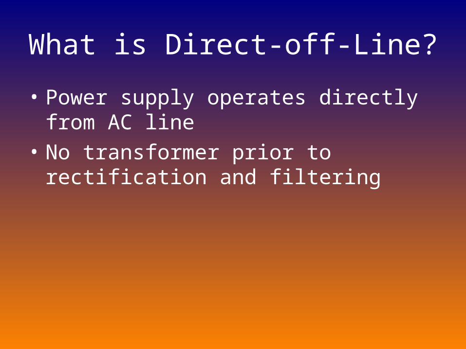
What is Direct-off-Line?
• Power supply operates directly from AC line
• No transformer prior to rectification and filtering

Switchmode vs. Linear
Switchmode Linear
Near constant efficiency and power load
Constant current load
Wide input voltage range Low cost
Low heat generation Low noise
High reliability Easy to use
Small size transformer Large bulky transformer
Frequency 100/300 kHz Frequency 50/60 Hz

Types of Switchmode Supplies
• Flyback topology
• Forward topology
• Half Bridge topology
• Push-Pull topology
• Full-Bridge topology

Typical Off-line Dual Voltage Rectifier, Filter Circuit

Off-lineAC Power Line
Series ResistanceESR
DC-DC ConverterLoad

Characteristics
• Voltage Operation (120Vac/240Vac)– 120V operation for voltage doubler– 240V operation for full-bridge rectifier
• Effective Series Resistance– Source resistance – reduce peak currents
20mOhms – 600mOhms.– Inrush Limiting thermistor – used for startup– 1Ohm

Characteristics
• Constant Power Load– Output voltage fixed under steady state
conditions• Near Constant efficiency for load• Rising Current
• Resistance Factor– Parameter used for calculating current loads

Designing
• Effective Input Current Ie
• RMS Input Current Iin(rms)
• Capacitor Current (Icap)
• Peak Input Current (Ipeak)
• Capacitor Size (Ce)
• DC Output voltage (Vo)

Designing

Designing

Simulation
E1
D1D2
D3 D4
RS
Ce
VM1.V [V] Vload.V [V] RS.R [Ohm]
t [s]
0.25k
-25
50
0.1k
0.15k
0.2k
0 50m5m 10m15m20m25m30m35m40m
+
V
VM1
Simplified Capacitive Input Filter w/ Single-PhaseFull/Wave Bridge Rectifer and Lumped Total EffectiveSource Resistance.
Converter loadRL
R := 425
C := 375uAMPL := 0.240416305603426k
FREQ := 50
70,7%
RMS
VinRMS
VinRMS.VAL
t [s]
0.2k
-20
25
50
75
0.1k
0.13k
0.15k
0.18k
0 10.2 0.4 0.6 0.8
VinRMS.VAL 0.169913k
R := .42
MEAN VALUE
Vout_DC
Vout_DC.VAL
t [s]
0.25k
-25
50
0.1k
0.15k
0.2k
0 10.2 0.4 0.6 0.8
Vout_DC.VAL
0.232103k
70,7%
RMS
Icap_rms
Icap_rms.VAL
2.07848
Icap_rms.VAL Ce.I [A]
t [s]
30
-5
0
5
10
15
20
25
0 50m5m 10m 15m 20m 25m 30m 35m 40m
70,7%
RMS
Ie
Ie.VAL 2.16092 A
Ipeak
W
+
WM1
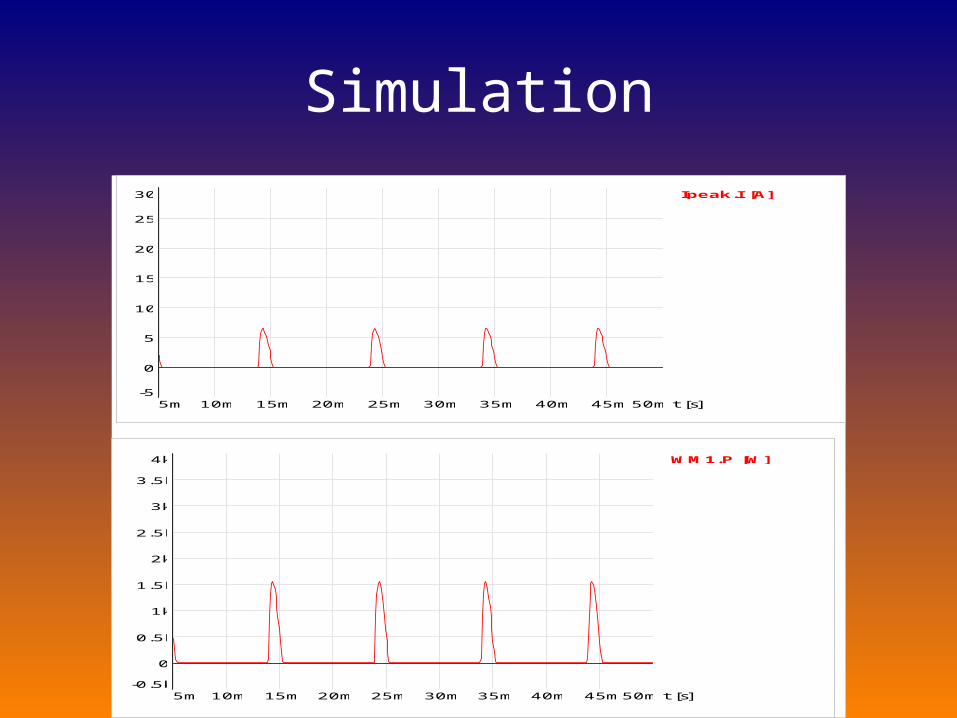
Simulation
Ipeak.I [A]
t [s]
30
-5
0
5
10
15
20
25
5m 50m10m 15m 20m 25m 30m 35m 40m 45m
WM1.P [W]
t [s]
4k
-0.5k
0
0.5k
1k
1.5k
2k
2.5k
3k
3.5k
5m 50m10m 15m 20m 25m 30m 35m 40m 45m

Simulation
1.260
1.280
1.300
1.320
1.340
1.360
1.380
1 10 100 1000
Power
Vo
(dc)/
Vin
(rm
s)
152.8
152.9
152.8
153
152.9
152.9
152.7

Calculations• Given parameters: Vin(rms) = 170 V• η = 0.7• Rs = 0.42 Ω• Pout = 250 W• F = 50 Hz• To find the minimum capacitance size of Ce, from Fig. 1.6.7, assume capacitance/Watt is 1.5 uF/W.• Ce = (1.5 uF)*(250 W) = 375 uF• The input power Pin can be found from the efficiency η.• Pin = Pout/η = 357 W @ 100% of load• Using Eq. #2, the effective input current Ie = 2.1 A• Using Eq. #4, the resistance factor Rsf = 150 Ω∙W• From Fig. 1.6.4 w/ 100% load, Rsf ratio yields Iin(rms)/Ie = 1.48. The input current is:• Iin(rms) = (2.1 A)*(1.48) = 3.11 A• From Fig. 1.6.5 w/ 100% load, Rsf ratio yields Icap(rms)/Ie = 1.3. The capacitor current is:• Icap(rms) = (2.1 A)*(1.3) = 2.73 A• From Fig. 1.6.6, Rsf ratio yields Ipeak/Ie = 4.6. The peak input current is:• Ipeak = (2.1 A)*(4.6) = 9.66 A• As discussed earlier in the DC Output Voltage and Regulation For Rectifier Capacitor Input Filters
section, when using Fig. 1.6.7:• (2πf)*(Ce)*(RL) > 50• So the load resistance RL >= 425 Ω. I used RL at its minimum value.• From Fig. 1.6.7 w/ Pin = 357 W and Rs = 0.42 Ω, the ratio Vo(dc)/Vin(rms) = 1.34. The filter DC output
voltage is: • Vo(dc) = 228 V.
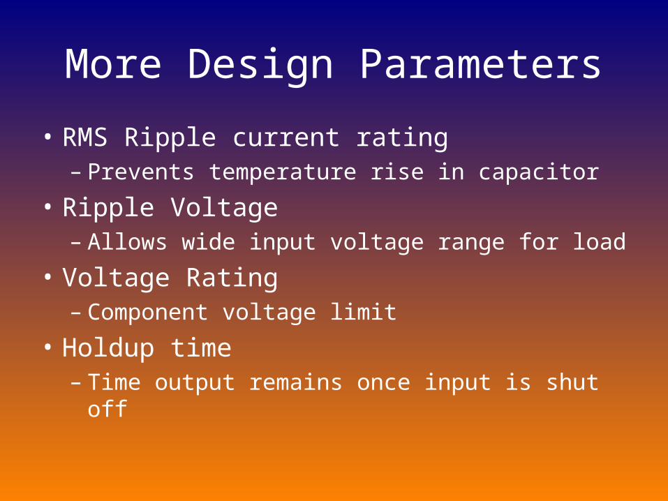
More Design Parameters
• RMS Ripple current rating– Prevents temperature rise in capacitor
• Ripple Voltage– Allows wide input voltage range for load
• Voltage Rating– Component voltage limit
• Holdup time– Time output remains once input is shut off

Applications
• Typically used in Digital Electronics– Cell Phones– PDA’s– PC’s– Laptops– CD/DVD Players

Applications
3.6 W Cell Phone Charger from Power Integration’s TINYSWITCH