Embed Size (px)
Citation preview
LIFETIME ESTIMATION OF POWER MOSFETS
By
Petros G. Taskas
A THESIS
Submitted to Michigan State University
in partial fulfillment of the requirements for the degree of
Electrical Engineering – Master of Science
2016
ABSTRACT
LIFETIME ESTIMATION OF POWER MOSFETS
By
Petros G. Taskas
In this document a theory is proposed that all power MOSFETs will go through
three regions of operation during their lifetime with respect to the threshold voltage.
Equations are presented for this proposed theory and analytical assumptions are made.
The first region that will be examined is when the MOSFET is healthy and all
parameters of the MOSFET are kept constant. The second region of operation is when
the gate oxide begins to degrade and the threshold voltage begins to dip. The third
region of operation is when Fowler-Nordheim tunneling begins to dominate the
threshold voltage of the device and the threshold voltage begins to continuously rise.
An accelerated aging experiment was conducted to try and prove the proposed
theory. Adverse effects were seen in the devices tested and the regions of operation
were modified in order to account for the large shift in the threshold voltage. Here the
proposed equations were reformulated to account for the different trapped charges in
the device throughout its lifetime. The equations formulated differ from the proposed
theory and are presented as new findings for the different regions of operation for power
MOSFETs. Data was also collected to calculate the turn on resistance and these
findings will be published at a later date. A final conclusion is given based on the data
collected and the different effects seen that account for the threshold voltage change in
power MOSFETs. This new theory may also be applied to insulated-gate bipolar
transistors (IGBTs) and various other power MOSFETs.

iii
ACKNOWLEDGEMENTS
I would like to thank my advisor Dr. Peng for his continuous guidance and support
during my time at Michigan State University. Dr. Peng’s dynamic, extensive, and
innovative knowledge in the field has been a great help to me throughout my research
assistantship from my undergraduate years to the completion of my Masters program.
None of this work would have been possible without Dr. Peng’s continuous guidance,
support, and offer into the Master’s program.
I would like to thank my committee members Dr. Sepúlveda and Dr. Wang for their help
and guidance during my thesis research.
I would like to thank Dr. Albrecht for his support and willingness to sit down with me to
talk about the numerous effects and concepts in MOSFETs. This helped me a great
deal with my conclusion.
I would like to thank my parents Georgios and Fani, my brother Athanasios, and my
sister Stefani for their continuous love and support throughout my six and half years of
university. Thank you for pushing me to do my best. I would like to thank my
grandmothers Aspasia Taskas and Stavroula Maggos for their continuous love and
support. I would like to thank Jaclyn Konopka for her support and help editing my thesis.
I would also like to thank the Hattar family, parents Fares and Khalida, brothers Zaid,
Murad, Odai, and Machail, for being with me throughout the years. Thank you for
becoming a part of my family. You are all invaluable to me.

iv
I would like to thank my lab mates for their help throughout my time in the research lab
and I would like to thank Ujjwal for the proposed theory in chapter 3. I would like to also
thank Ameer Janabi for discussing numerous concepts with me.
Lastly I would like to thank my friends Annie Elshoff, Aaron Brakoniecki, Terry Pharaon,
Po-yuan Han, Sierra Santia, and Junseo Jung for their support and guidance through
the numerous obstacles I encountered during my time at Michigan State University.
Your help was greatly appreciated.
v
TABLE OF CONTENTS
LIST OF TABLES ........................................................................................................... vii
LIST OF FIGURES ........................................................................................................ viii
Chapter 1 Introduction to Power MOSFETs ............................................................... 1
Chapter 2 Power MOSFET Background ..................................................................... 3 2.1 Power MOSFET ............................................................................................... 3
2.1.1 V-MOSFET Structure ................................................................................. 3
2.1.2 VD-MOSFET Structure .............................................................................. 4
2.1.3 U-MOSFET Structure................................................................................. 6
2.2 Failures Due to Thermo-Mechanical Stress...................................................... 7
2.2.1 Bond-wire Cracking and Liftoff ................................................................... 8
2.2.2 Die-attach Degradation and Failure ......................................................... 10
2.3 Electrical Failures of Power MOSFETs .......................................................... 11
2.3.1 Gate Oxide Breakdown ............................................................................ 11
2.3.2 Maximum Drain to Source Voltage Breakdown ....................................... 12
Chapter 3 Proposed Lifetime Theory ........................................................................ 14 3.1 Introduction ..................................................................................................... 14 3.2 General Theory for Identification of Key Operating Regions in Power
MOSFETs ....................................................................................................... 16
3.3 Variation of Failure Precursors Based on Proposed Theory ........................... 18
3.4 Variation of Threshold Voltage ....................................................................... 19
3.5 Analytical Interpretation .................................................................................. 21
3.6 Conclusion ...................................................................................................... 23
Chapter 4 Accelerated Aging Process ..................................................................... 24 4.1 Test Setup ...................................................................................................... 24
4.1.1 Power MOSFET Test Circuit .................................................................... 25
4.1.2 Test Circuit Equipment............................................................................. 25
4.1.3 Data Acquisition Equipment ..................................................................... 26
4.2 Test Procedure ............................................................................................... 28
4.2.1 Normal Operation of the Power MOSFET ................................................ 28
4.2.2 Aging the Power MOSFET ....................................................................... 28
4.2.3 Data Acquisition ....................................................................................... 29
4.3 Thermomechanical Stress Isolation from Electrical Stresses ......................... 31
4.4 C-V Measurement .......................................................................................... 32
4.5 Annealing........................................................................................................ 32
vi
Chapter 5 Evaluation of Test Data............................................................................ 34
5.1 Test Data ........................................................................................................ 34 5.2 Critical Evaluation ........................................................................................... 38
5.2.1 Introduction .............................................................................................. 38
5.2.2 Evaluation with Respect to the Proposed Theory .................................... 39
5.2.3 Evaluation with Respect to the more Probable Solution .......................... 41
5.3 Future Work .................................................................................................... 48
5.4 Conclusion ...................................................................................................... 50
BIBLIOGRAPHY ........................................................................................................... 52
vii
LIST OF TABLES
Table 5.2.1: MOSFET Switching Table ........................................................................ 43
viii
LIST OF FIGURES
Figure 1.1: Single Phase Inverter using MOSFETs ......................................................... 1
Figure 2.1.1: V-MOSFET Structure ................................................................................. 4
Figure 2.1.2: VD-MOSFET Structure ............................................................................... 5
Figure 2.1.3: U-MOSFET Structure ................................................................................. 7
Figure 2.2.1: von-Mises Distribution ................................................................................ 9
Figure 2.2.2: Bond-wire Liftoff ......................................................................................... 9
Figure 2.2.3: Die-attach to Copper ................................................................................ 10
Figure 2.3.1: High Resolution Transmission Electron Micrograph ................................. 12
Figure 2.3.2: Snapback Breakdown .............................................................................. 13
Figure 3.2: Effects of Gate Oxide Degradation (a) Formation of Localized Conduction Path. (b) Enhanced Electron Trapping .......................................................................... 18
Figure 3.5: Variation of Threshold Voltage with Aging................................................... 22
Figure 4.1.1: Test Circuit Configuration ......................................................................... 25
Figure 4.1.2: Test Circuit ............................................................................................... 26
Figure 4.1.3: Test Setup with DAQ ................................................................................ 27
Figure 4.2.3: Stressing and Data Acquisition Process................................................... 30
Figure 5.1.1: MOSFET Threshold Voltage Due to Aging ............................................... 36
Figure 5.1.2: MOSFET Gate Capacitance Due to Aging ............................................... 37
Figure 5.2.3: Hole Trapping, Annealing, and Reversible Compensation ....................... 44

1
Chapter 1
Introduction to Power MOSFETs
A power metal-oxide-semiconductor field-effect-transistor (MOSFET) is a type of electric
switch that can be programmed through a digital signal processor to turn on and off.
Power MOSFETs also have different voltage and current ratings, which can be used for
many applications. Power MOSFETs are used in a wide variety of applications from
home Do It Yourself projects to commercial projects. Some of the major uses for power
MOSFETs are inverters, buck and boost converts as well as AC/AC and DC/DC
converters. Figure 1.1 shows a single phase inverter using MOSFETs. Here Vd is the
drain to source voltage and Vo is the output voltage.
Figure 1.1 Single Phase Inverter using MOSFETs
2
The different topologies mentioned above can be applied to and are not limited to hybrid
and fully electric vehicles, solar panel systems, induction heating, electroshock
weapons, and household appliances such as refrigerators or electric ovens. Today
these devices are becoming more and more prominent in many different applications as
can be seen with vehicles transitioning more towards hybrid, electric, and autonomous
vehicles. A major issue raised by power MOSFETs increase in use is their reliability and
which trends and parameters should be taken into consideration in estimating remaining
lifetime. These trends in the different parameters that can be measured may correlate to
the reliability of the device. For example, temperature monitoring of the device is
important to make sure that it does not exceed the rating of the device specified by the
data sheet. In the industry, the reliability of these devices is very important because of
the important applications they are used in. For instance, when purchasing a hybrid or
electric vehicle, the consumer will not want to go back to the dealership every thousand
or five thousand miles driven to get the inverter replaced because the power MOSFETs
have failed again. It is therefore vital to study MOSFET reliability, trends, and
parameters so that they can be safely and efficiently used in important daily appliances.
Not only can the failure or malfunction of power MOSFETs cause the inverter to get
damaged but it can cause other electric components such as the electric motor to fail
without the correct protection and will ultimately cause distrust between the consumer
and the product. Monitoring key parameters such as threshold voltage, is a must to
make inverters and other topologies more reliable and efficient.
3
Chapter 2
Power MOSFET Background
The following is a general description of the main properties and models of power
MOSFETs. The MOSFETs are examined are the V-MOSFET, VD-MOSFET, and the U-
MOSFET all from [8]. Different failure profiles of the devices are also explained.
2.1 Power MOSFET
2.1.1 V-MOSFET Structure
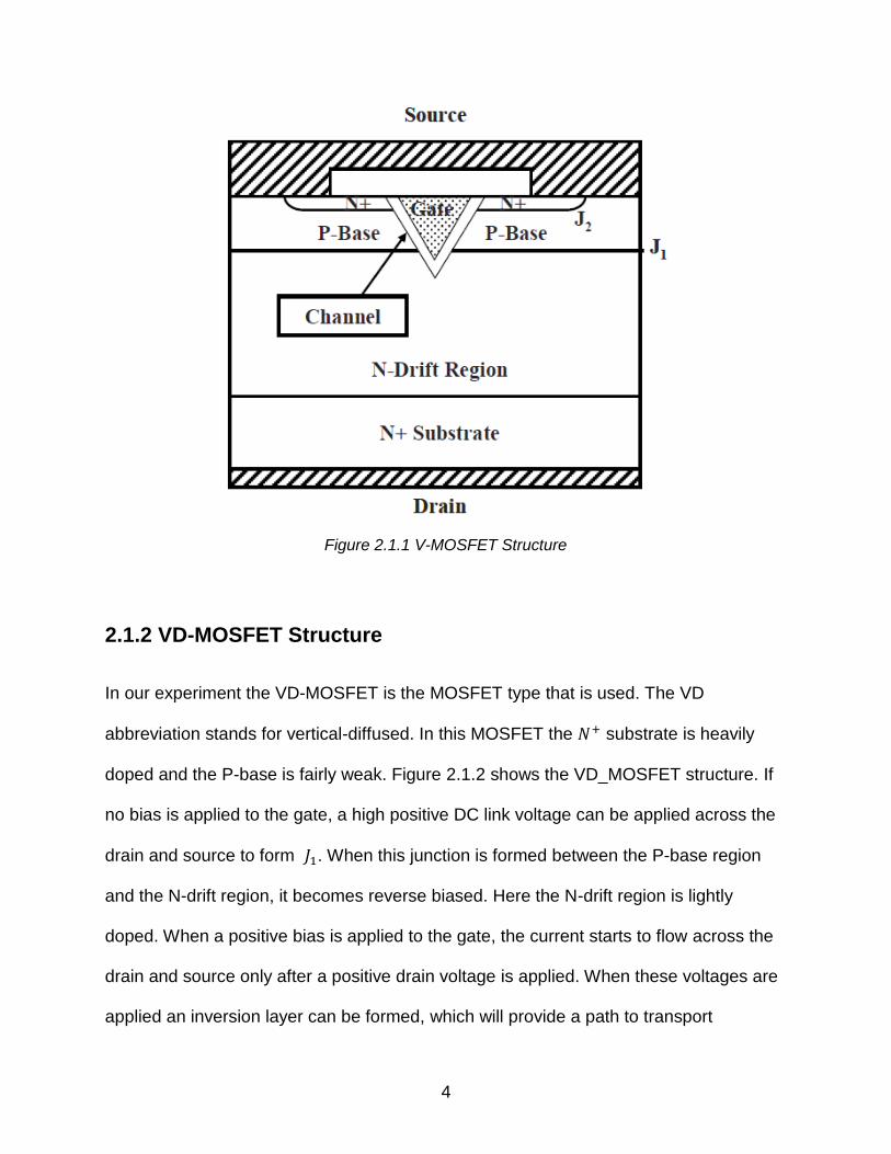
The V-MOSFET structure was developed in the 1970s. This structure has the 𝑁+
source separated from the drain by a P-base region. As seen in figure 2.1.1 [8], the gate
is a V-groove and goes through the P-base region into the N-drift region. The oxide is
on the surface of the V-groove. Without any bias applied to the gate, 𝐽1 becomes
reverse biased if the drain electrode has a positive bias applied to it. Next we have 𝐽2,
which is overlapping the source electrode over the junction. It is noted that 𝐽2 is short
circuited due to this overlap. When a positive gate bias is applied to the gate, it attracts
electrons under the gate oxide to the semiconductor surface which provides a path for
current flow from the source and drain of the MOSFET. Here the internal resistance of
the MOSFET restricts the maximum allowable current the MOSFET can carry. The V-
MOSFET structure is no longer used due to various manufacturing difficulties.
4
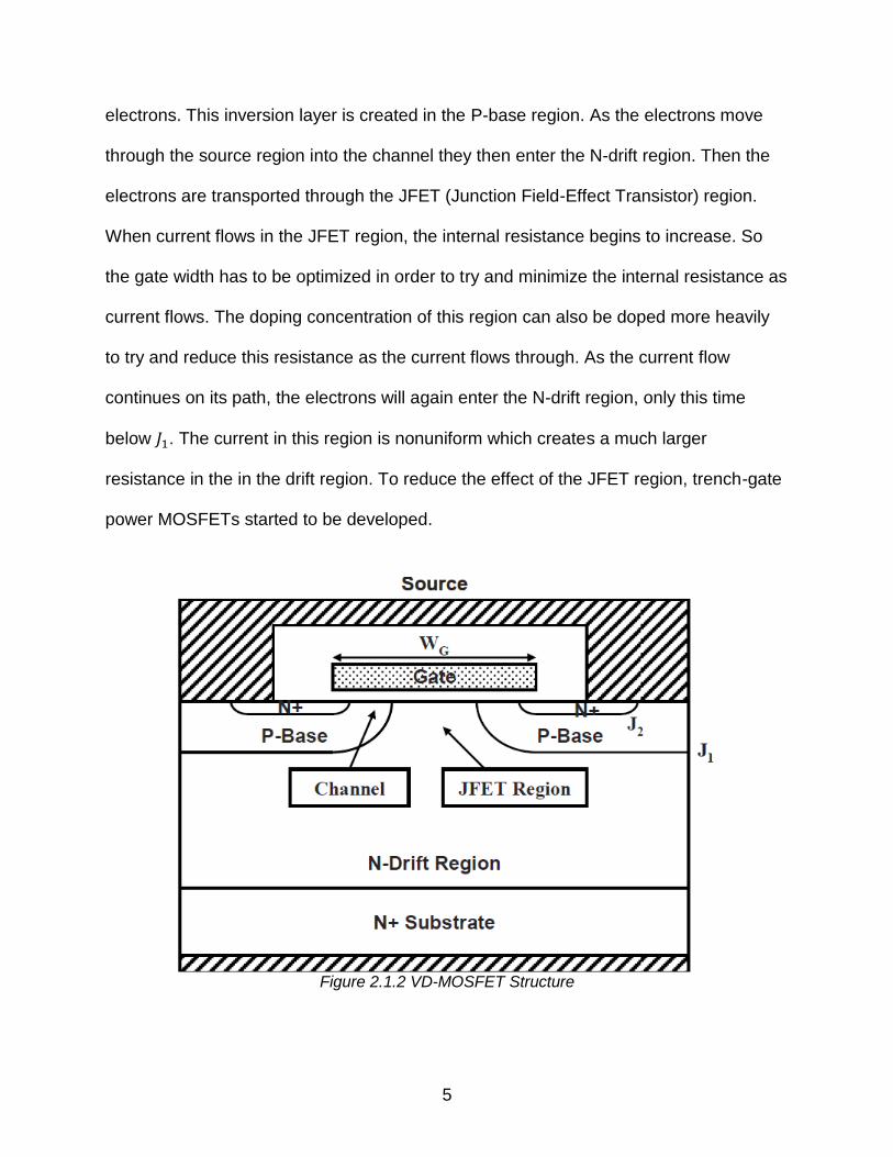
2.1.2 VD-MOSFET Structure
In our experiment the VD-MOSFET is the MOSFET type that is used. The VD
abbreviation stands for vertical-diffused. In this MOSFET the 𝑁+ substrate is heavily
doped and the P-base is fairly weak. Figure 2.1.2 shows the VD_MOSFET structure. If
no bias is applied to the gate, a high positive DC link voltage can be applied across the
drain and source to form 𝐽1. When this junction is formed between the P-base region
and the N-drift region, it becomes reverse biased. Here the N-drift region is lightly
doped. When a positive bias is applied to the gate, the current starts to flow across the
drain and source only after a positive drain voltage is applied. When these voltages are
applied an inversion layer can be formed, which will provide a path to transport
Figure 2.1.1 V-MOSFET Structure
5
electrons. This inversion layer is created in the P-base region. As the electrons move
through the source region into the channel they then enter the N-drift region. Then the
electrons are transported through the JFET (Junction Field-Effect Transistor) region.
When current flows in the JFET region, the internal resistance begins to increase. So
the gate width has to be optimized in order to try and minimize the internal resistance as
current flows. The doping concentration of this region can also be doped more heavily
to try and reduce this resistance as the current flows through. As the current flow
continues on its path, the electrons will again enter the N-drift region, only this time
below 𝐽1. The current in this region is nonuniform which creates a much larger
resistance in the in the drift region. To reduce the effect of the JFET region, trench-gate
power MOSFETs started to be developed.
Figure 2.1.2 VD-MOSFET Structure
6
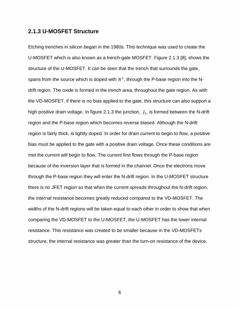
2.1.3 U-MOSFET Structure
Etching trenches in silicon began in the 1980s. This technique was used to create the
U-MOSFET which is also known as a trench-gate MOSFET. Figure 2.1.3 [8], shows the
structure of the U-MOSFET. It can be seen that the trench that surrounds the gate,
spans from the source which is doped with 𝑁+, through the P-base region into the N-
drift region. The oxide is formed in the trench area, throughout the gate region. As with
the VD-MOSFET, if there is no bias applied to the gate, this structure can also support a
high positive drain voltage. In figure 2.1.3 the junction, 𝐽1, is formed between the N-drift
region and the P-base region which becomes reverse biased. Although the N-drift
region is fairly thick, is lightly doped. In order for drain current to begin to flow, a positive
bias must be applied to the gate with a positive drain voltage. Once these conditions are
met the current will begin to flow. The current first flows through the P-base region
because of the inversion layer that is formed in the channel. Once the electrons move
through the P-base region they will enter the N-drift region. In the U-MOSFET structure
there is no JFET region so that when the current spreads throughout the N-drift region,
the internal resistance becomes greatly reduced compared to the VD-MOSFET. The
widths of the N-drift regions will be taken equal to each other in order to show that when
comparing the VD-MOSFET to the U-MOSFET, the U-MOSFET has the lower internal
resistance. This resistance was created to be smaller because in the VD-MOSFETs
structure, the internal resistance was greater than the turn-on resistance of the device.
7
2.2 Failures Due to Thermomechanical Stresses
As the temperature begins to rise in these devices, it starts to alter many physical
properties which can change the physics of the devices themselves. The mechanical
parameters that can change the electrical parameters of the device are bond-wire
cracking, bond-wire liftoff, die-attach degradation, and die-attach failure. These
parameters can change the turn on resistance which can affect the electrical
parameters of the device. Power cycling which leads to thermo-cycling is the main
cause of these failures.
Figure 2.1.3 U-MOSFET Structure
8
2.2.1 Bond-wire Cracking and Liftoff
Bond-wire cracking and liftoff are the most prominent areas of failure for power devices
[19]. Bond-wires degrade over time before these failures start occurring and over time
will cause a failure in the device. This is due to the applications they are used in and the
environments they are placed working in. For example, in hybrid vehicles, when left out
in the sun on a hot day, the whole inverter system gets even hotter than the ambient
outdoor temperature is because the heat is trapped. So if one was to turn the car on
and have the cooling system kick on full power to cool off the devices, that temperature
fluctuation could start to cause this cracking or liftoff of the bond-wires. The main cause
of the bond-wire liftoff is how the junction temperature fluctuates. If the junction its self is
fluctuating from 20° C to 150° C or higher and it keeps repeating, then this type of
failure is more likely. Also when systems are power cycled or thermo-cycled the junction
temperature is most likely to fluctuate. In order to try and keep this failure from
happening a cooling system must be integrated and used to control the junction
temperature of the device. The device case temperature should also be monitored when
cooling the device off. If cooling happens to fast causing the temperature of the device
to go lower than it needs to go, the device then has to heat up causing the cooling
system to shut off. This can lead to a temperature fluctuation process in which the
device heats up too much and then gets cooled off too fast to a temperature lower than
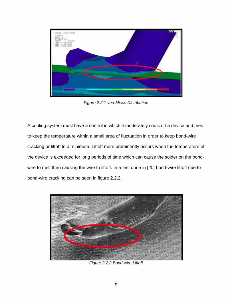
needed which would cause the bond-wires to crack or liftoff. Figure 2.2.1 from [20]
shows the von-Mises distribution which leads to the bond-wire cracking.
9
A cooling system must have a control in which it moderately cools off a device and tries
to keep the temperature within a small area of fluctuation in order to keep bond-wire
cracking or liftoff to a minimum. Liftoff more prominently occurs when the temperature of
the device is exceeded for long periods of time which can cause the solder on the bond-
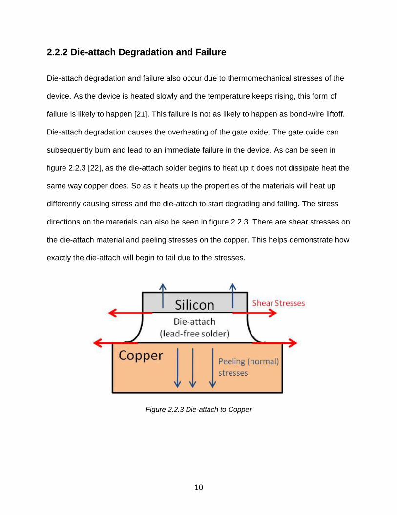
wire to melt then causing the wire to liftoff. In a test done in [20] bond-wire liftoff due to
bond-wire cracking can be seen in figure 2.2.2.
Figure 2.2.1 von-Mises Distribution
Figure 2.2.2 Bond-wire Liftoff
10
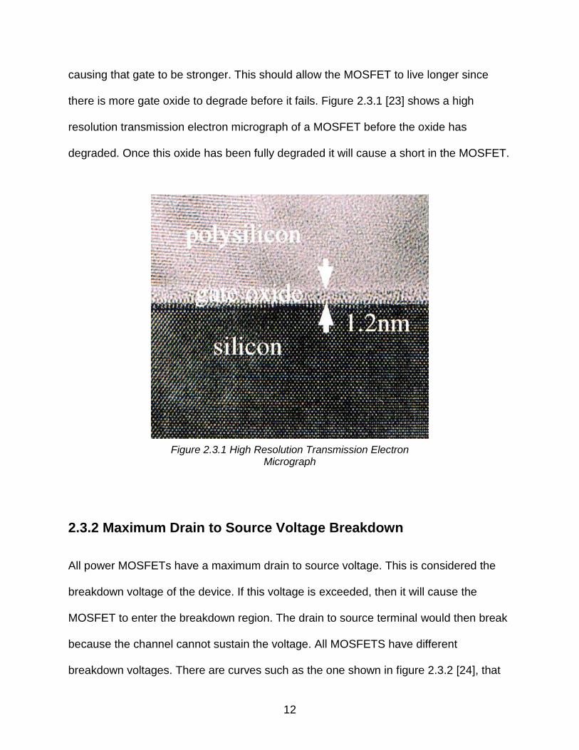
2.2.2 Die-attach Degradation and Failure
Die-attach degradation and failure also occur due to thermomechanical stresses of the
device. As the device is heated slowly and the temperature keeps rising, this form of
failure is likely to happen [21]. This failure is not as likely to happen as bond-wire liftoff.
Die-attach degradation causes the overheating of the gate oxide. The gate oxide can
subsequently burn and lead to an immediate failure in the device. As can be seen in
figure 2.2.3 [22], as the die-attach solder begins to heat up it does not dissipate heat the
same way copper does. So as it heats up the properties of the materials will heat up
differently causing stress and the die-attach to start degrading and failing. The stress
directions on the materials can also be seen in figure 2.2.3. There are shear stresses on
the die-attach material and peeling stresses on the copper. This helps demonstrate how
exactly the die-attach will begin to fail due to the stresses.
Figure 2.2.3 Die-attach to Copper

11
2.3 Electrical Failures of Power MOSFETs
The three types of electrical failures that will be briefly discussed are the gate oxide
breakdown, maximum drain to source voltage breakdown, and maximum drain current
breakdown.
2.3.1 Gate Oxide Breakdown
Gate oxide breakdown can be caused immediately or overtime. For the gate oxide to
break down immediately, a very high voltage applied across the gate and source would
be needed. This voltage would have to exceed the maximum rating of the device by up
to three or four times. The immediate breakdown due to overvoltage is unlikely to
happen in a real system due to protection circuitry from the gate drive. On the other
hand, over time the gate oxide will degrade due to potential over stresses on the device.
This can happen in a normally operating device. Every time the MOSFET is switched on
and off the voltage applied is an electrical stress to the gate. This means over time the
oxide will degrade. When the oxide is degrading this means that the thickness of the
dielectric material of the gate is decreasing throughout its life. As the oxide diminishes,
this can cause an immediate failure of the oxide once it becomes too thin. After the
oxide has degraded completely or it has broken after getting thin, the MOSFET will
immediately fail. Once the MOSFET fails due to the gate oxide degradation, the gate of
the MOSFET will be shorted to the drain and source causing the gate drive to start
supplying more current and no voltage. At this point control of the gate is lost and the
MOSFET is considered dead. Some MOSFETs have thicker gate oxide than others
12
causing that gate to be stronger. This should allow the MOSFET to live longer since
there is more gate oxide to degrade before it fails. Figure 2.3.1 [23] shows a high
resolution transmission electron micrograph of a MOSFET before the oxide has
degraded. Once this oxide has been fully degraded it will cause a short in the MOSFET.
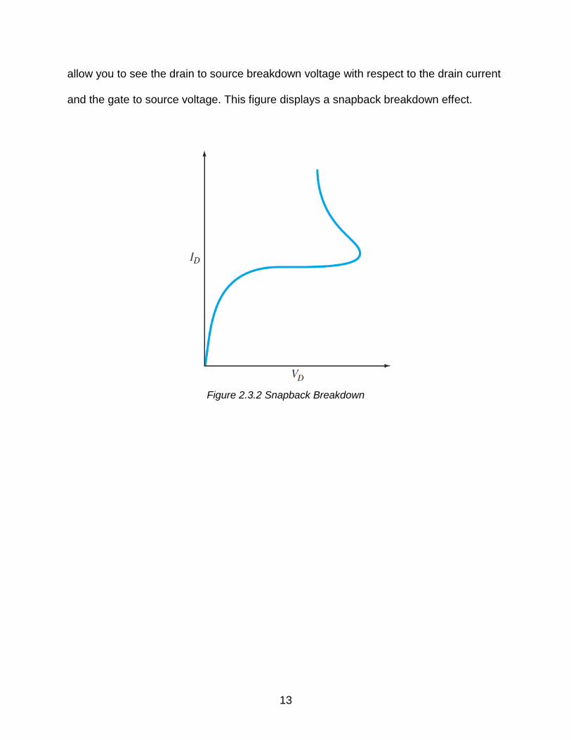
2.3.2 Maximum Drain to Source Voltage Breakdown
All power MOSFETs have a maximum drain to source voltage. This is considered the
breakdown voltage of the device. If this voltage is exceeded, then it will cause the
MOSFET to enter the breakdown region. The drain to source terminal would then break
because the channel cannot sustain the voltage. All MOSFETS have different
breakdown voltages. There are curves such as the one shown in figure 2.3.2 [24], that
Figure 2.3.1 High Resolution Transmission Electron Micrograph
13
allow you to see the drain to source breakdown voltage with respect to the drain current
and the gate to source voltage. This figure displays a snapback breakdown effect.
Figure 2.3.2 Snapback Breakdown

14
Chapter 3
Proposed Lifetime Theory
3.1 Introduction
This chapter will explain why and how gate oxide degradation plays a prominent role in
power MOSFET failure. A general theory has been proposed that power MOSFETs go
through three operating regions as gate oxide degradation occurs. In region I, the gate
oxide is not aged and considered to be fresh and healthy. In region II, the gate oxide
has started aging and the degradation of the oxide initiates. In region III, Fowler-
Nordheim tunneling of electrons begins to occur in the gate oxide. The physics behind
gate oxide degradation will be explained and shown with analytical equations that show
a “dip and rebound” phenomenon in the threshold voltage throughout the three
operating regions of the power MOSFET. The “dip and rebound” of threshold voltage
with the gate oxide degrading as it ages helps to determine the health of power
MOSFETs. This also provides an advanced warning for power MOSFET failures. Lastly,
this pinpoints the instant of failure initiation due to oxide degradation and point of critical
failure in power MOSFETs.
Power MOSFETs are a crucial component of power converters used in high voltage and
high power applications. Since the reliability of power MOSFETs is critical to the
operation of these power converters, effective forecasting of power MOSFET failures is
essential. Prognosis can be defined as a forecast of a likely failure with the help of a
15
failure precursor- an indicator of impending failure [1]. The key failure precursors of
power MOSFETs with aging identified in the literature are: Threshold voltage, VTH [2]-
[5], shift in threshold voltage [5], and switching time variations [6]. Aging and gate oxide
degradation are very closely related and plays a prominent role in power MOSFET
failure. However, the variation of the threshold voltage with aging due to oxide
degradation is not consistent across all literature. The threshold voltage (VTH) of a
power MOSFET is reported to increase with aging [3]-[4], whereas other studies have
found the threshold voltage is to “dip and rebound” with aging [5]-[6]. To explain this
difference in failure precursor variation with gate oxide degradation, the general theory
is proposed that power MOSFETs go through three distinct operating regions as gate
oxide degradation occurs over time. The identification of three operating regions
alternatively helps us determine the “health” of power MOSFETs.
1) Region I (Normal operation region):
This region corresponds to the operation of power MOSFETs before the initiation
of gate oxide degradation. The failure precursors remain constant in this region and do
not affect the MOSFET which will be regarded as “healthy”.
2) Region II (Operation after initiation of gate oxide degradation):
The gate oxide, like any other dielectric, degrades over time. This region
corresponds to the operation of power MOSFETs after the initiation of gate oxide
degradation. In this case, the MOSFET aging process has begun and started to take an

16
effect and the failure precursors have begun to show some variation, “dip and rebound”
with oxide degradation and the MOSFET can be regarded as “sick”.
3) Region III (Operation after initiation of Fowler-Nordheim tunneling of electrons into
the oxide):
With gradual gate oxide degradation, the oxide field increases to a point where
Fowler-Nordheim tunneling [9] of electrons occurs in gate oxide and the failure
precursors start to show accelerated aging characteristics. The power MOSFET
operating in this region can be regarded as “dying”.
3.2 General Theory for Identification of Key Operating
Regions in Power MOSFETs
Gate oxides, like any other dielectric, when stressed under an electric field degrades
over time and eventually breaks down. The failure precursors of Power MOSFETs vary
with gate oxide degradation. The identification of key operating regions of power
MOSFETs due to gate oxide degradation can be explained with the existing physics of
gate oxide degradation.
I. Region I (Normal operation region)
A fresh oxide has a finite dielectric thickness. The gate oxide is assumed to
maintain its thickness over a long period of time after which it slowly begins to degrade.
The failure precursors remain constant in this operating region as the gate oxide
degradation and aging have not initiated yet.
17
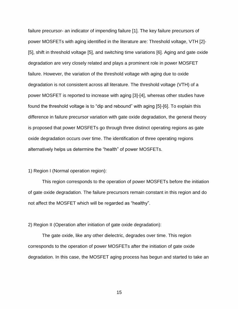
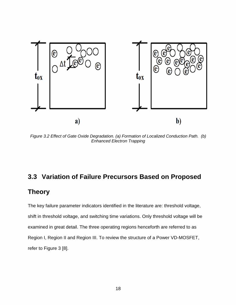
II. Region II (Operation after initiation of gate oxide degradation)
Even with a very low field stress, the degradation of the gate oxide begins to
occur over time. The thermo-mechanical or (E) model explains the breakdown of SiO2
oxide in terms of field enhanced bond breakage under low field stress [10]-[11]. The Si-
Si bond breakage leads to formation of traps which create localized conduction paths in
the oxide. The increase in localized conduction paths in the oxide can be considered
equivalent to thinning of the gate oxide, as indicated by ∆t, a reduction of gate oxide
thickness in figure 3.2a. We introduce the word “effective gate oxide thickness” to take
into account the reduction of gate oxide thickness due to localized conduction paths as
a result of charge trapping. The effective gate oxide thickness does not necessarily
indicate the uniform reduction of overall gate oxide thickness; rather it indicates the
localized reduction of gate oxide thickness due to formation of localized conducting links
in the gate oxide.
III. Region III (Operation after Initiation of Fowler-Nordheim tunneling of electrons into
oxide)
With continuous reduction of gate oxide thickness, the oxide field begins to
increase. When the oxide field is in the range of 5-7 MV/cm [12]-[14], Fowler-Nordheim
(FN) tunneling of electrons dominates in the oxide [11]-[13], [15]-[16] which contributes
to hole generation and trapping. As a result, enhanced electron trapping occurs in the
oxide as shown in figure 3.2b and the nature of the trapped charges is negative [4], [15]-
[18].
18
3.3 Variation of Failure Precursors Based on Proposed
Theory
The key failure parameter indicators identified in the literature are: threshold voltage,
shift in threshold voltage, and switching time variations. Only threshold voltage will be
examined in great detail. The three operating regions henceforth are referred to as
Region I, Region II and Region III. To review the structure of a Power VD-MOSFET,
refer to Figure 3 [8].
Figure 3.2 Effect of Gate Oxide Degradation. (a) Formation of Localized Conduction Path. (b) Enhanced Electron Trapping
19
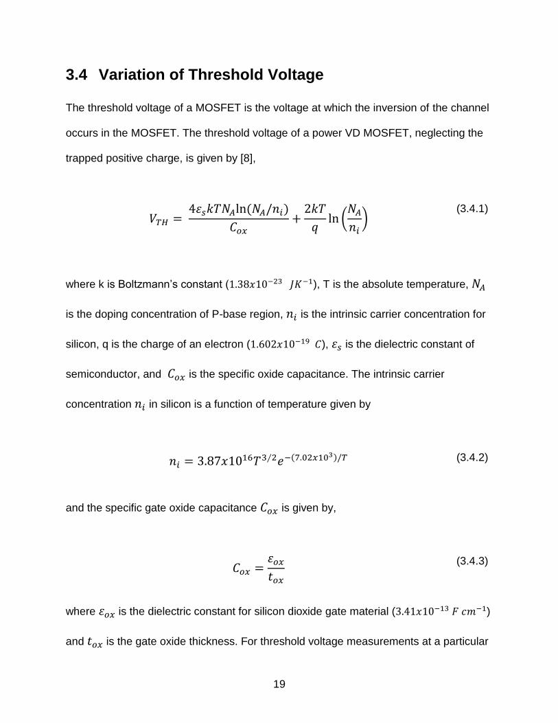
3.4 Variation of Threshold Voltage
The threshold voltage of a MOSFET is the voltage at which the inversion of the channel
occurs in the MOSFET. The threshold voltage of a power VD MOSFET, neglecting the
trapped positive charge, is given by [8],
𝑉𝑇𝐻 = 4𝜀𝑠𝑘𝑇𝑁𝐴ln (𝑁𝐴/𝑛𝑖)
𝐶𝑜𝑥+
2𝑘𝑇
𝑞ln (
𝑁𝐴
𝑛𝑖)
(3.4.1)
where k is Boltzmann’s constant (1.38𝑥10−23 𝐽𝐾−1), T is the absolute temperature, 𝑁𝐴
is the doping concentration of P-base region, 𝑛𝑖 is the intrinsic carrier concentration for
silicon, q is the charge of an electron (1.602𝑥10−19 𝐶), 𝜀𝑠 is the dielectric constant of
semiconductor, and 𝐶𝑜𝑥 is the specific oxide capacitance. The intrinsic carrier
concentration 𝑛𝑖 in silicon is a function of temperature given by
𝑛𝑖 = 3.87𝑥1016𝑇3∕2𝑒−(7.02𝑥103)/𝑇 (3.4.2)
and the specific gate oxide capacitance 𝐶𝑜𝑥 is given by,
𝐶𝑜𝑥 =𝜀𝑜𝑥
𝑡𝑜𝑥
(3.4.3)
where 𝜀𝑜𝑥 is the dielectric constant for silicon dioxide gate material (3.41𝑥10−13 𝐹 𝑐𝑚−1)
and 𝑡𝑜𝑥 is the gate oxide thickness. For threshold voltage measurements at a particular
20
temperature, the threshold voltage is a function of gate oxide capacitance alone, or
alternatively the gate oxide thickness, as intrinsic carrier concentration in (3.4.2)
becomes constant.
1) Region I
In operating region I, the gate oxide is assumed to be fresh without any
degradation. Since the gate oxide thickness remains the same, the threshold voltage
given by (1) is constant in this operating region.
2) Region II
In operating region II, the initiation of oxide degradation leads to thinning of gate
oxide or alternatively, an increase in gate capacitance. The oxide thickness 𝑡𝑜𝑥 is
represented by equivalent gate oxide thickness 𝑡𝑜𝑥,𝑒𝑞 to take into account the reduction
of gate oxide thickness in equation (3.4.1)
𝑉𝑇𝐻 =𝑡𝑜𝑥,𝑒𝑞
𝜀𝑜𝑥(√4𝜀𝑠𝑘𝑇𝑁𝐴ln (𝑁𝐴/𝑛𝑖)) +
2𝑘𝑇
𝑞ln (
𝑁𝐴
𝑛𝑖)
(3.4.4)
The second term of the threshold voltage in equation (3.4.4) can be ignored as it
is small compared to its first term [8]. The threshold voltage decreases with reduction of
gate oxide thickness.
21
3) Region III
In operating region III, the oxide field reaches the FN threshold allowing a path
for FN electrons to flow. It leads to enhanced electron trapping in the oxide, which can
be taken into account by introducing negative trapped charge 𝑄𝑡𝑟𝑎𝑝 in (3.4.1) as
𝑉𝑇𝐻 =√4𝜀𝑠𝑘𝑇𝑁𝐴ln (𝑁𝐴/𝑛𝑖)
𝐶𝑜𝑥+
2𝑘𝑇
𝑞ln (
𝑁𝐴
𝑛𝑖) +
𝑄𝑡𝑟𝑎𝑝
𝐶𝑜𝑥
(3.4.5)
The threshold voltage in equation (3.4.5) begins to increase because of trapped
charges. The gate oxide continues to degrade but the threshold voltage increases as
trapped charges become dominant in equation (3.4.5).
3.5 Analytical Interpretation
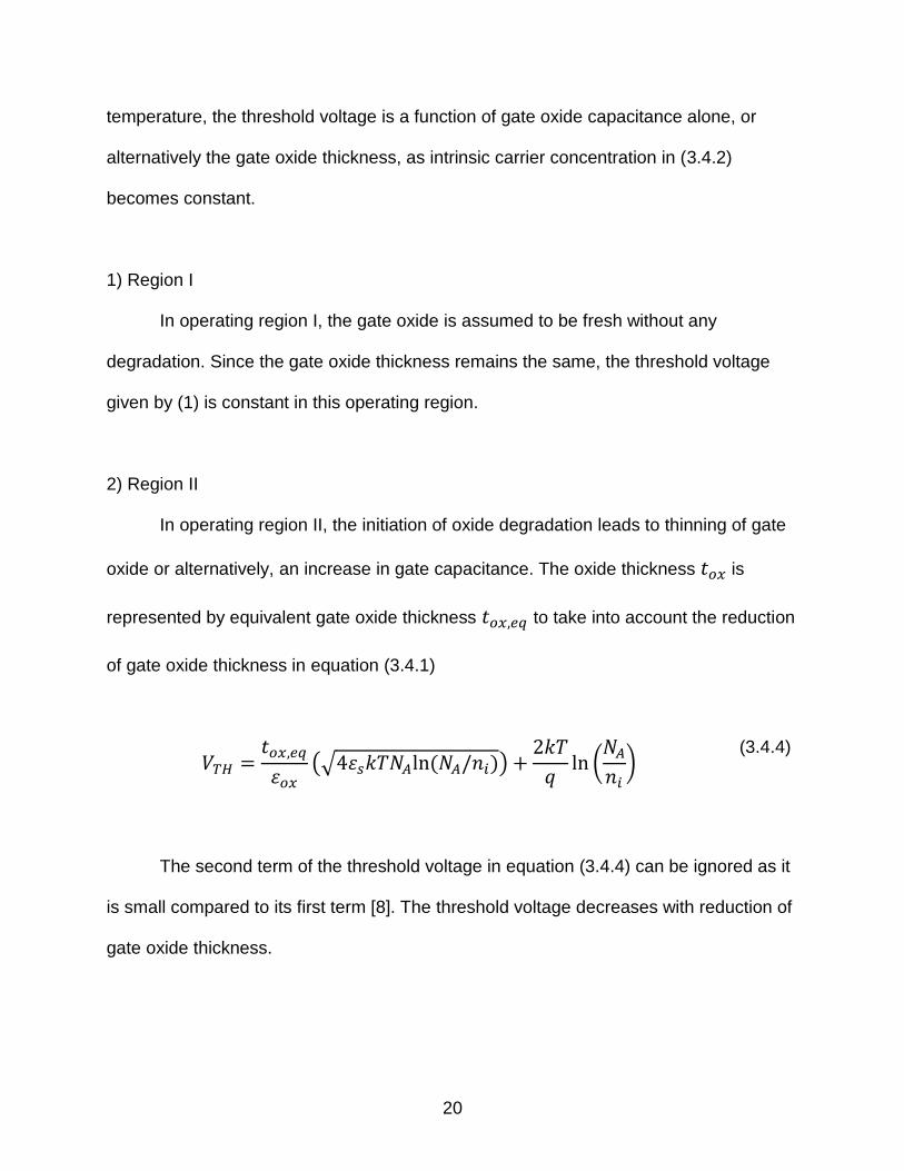
Figure 3.5 shows the variation of threshold voltage in power VD-MOSFET in three
operating regions based on analytical expressions (1)-(5).Initially, the gate oxide is fresh
and the power MOSFET is said to be operating in Region I. The threshold voltage is
constant in this region as the gate oxide thickness is assumed to remain constant in
equation (3.4.1). After the initiation of gate oxide degradation, the power MOSFET is
said to be operating in region II where the threshold voltage decreases/dips due to
thinning of gate oxide as given by equation (3.4.4). The decrease in threshold voltage
continues until the gate oxide degrades to a thickness permitting an oxide field of 7
MV/cm at which the FN tunneling starts to occur.
22
The equivalent oxide thickness corresponding to an oxide field of 7 MV/cm for initiation
of FN tunneling is nearly 285 Å. After the initiation of FN tunneling, the MOSFET is said
to be operating in Region III where the threshold voltage begins to increase/rebound as
given by equation (3.4.5). In order to show the effect of trapped charges, a fixed oxide
thickness of 285 Aº is used in equation (3.4.5) while sweeping the trapped charges. The
“dip” is an indicator of failure initiation in power MOSFETs. It does not mean that the
power MOSFET is nonoperational; rather it indicates that the power MOSFET has
started to show signs of aging. The “rebound” stage, on the other hand, is a critical
stage warning an imminent failure of a power MOSFET. The device could be non-
operational at any instant signifying complete loss of gate control. It should be pointed
Figure 3.5 Variation of Threshold Voltage with Aging
23
out that the theory explains both the rebound behavior in [3]-[4], and the dip and
rebound behavior in [5]-[6] for threshold voltage in power MOSFETs.
3.6 Conclusion
This is a proposed general theory that power MOSFETs go through three operating
regions over the course of gate oxide degradation. It has been shown that the variation
of failure precursors, mainly the threshold voltage shows an interesting “dip and
rebound” phenomenon in newly identified operating regions. The dip and rebound of the
threshold voltage in these operating regions is helpful to: i) determine the health of
power MOSFETs, ii) provide advance warnings for MOSFET failures, and iii) pinpoint
the instant of failure initiation and critical failure in power MOSFETs. The theory
presented can be extended to IGBT failure as well.

24
Chapter 4
Accelerated Aging Process
This chapter will focus on the testing setup and testing process of the Power MOSFET.
The testing setup will consist of what MOSFET was used, the components in the testing
circuit, and the equipment that was used to measure and monitor the different voltage,
current and temperature parameters throughout the entire test. The testing process will
go through in detail the stressing circuit and the normal operation circuit and how they
are both isolated from each other. The isolation of applied thermomechanical stresses
from electrical stresses will also be explained and the reasons behind the importance of
this isolation.
4.1 Test Setup
The test setup consists of a stressing circuit to age the MOSFET and a circuit that runs
the MOSFET under normal operating conditions. These circuits are integrated together
with three physical switches that can be opened and closed in order to isolate stressing
from normal operation.
25
4.1.1 Power MOSFET Test Circuit
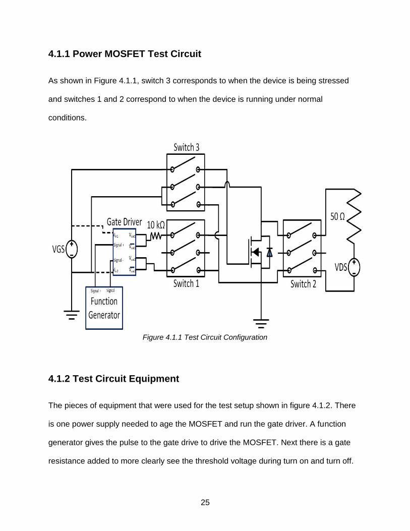
As shown in Figure 4.1.1, switch 3 corresponds to when the device is being stressed
and switches 1 and 2 correspond to when the device is running under normal
conditions.
4.1.2 Test Circuit Equipment
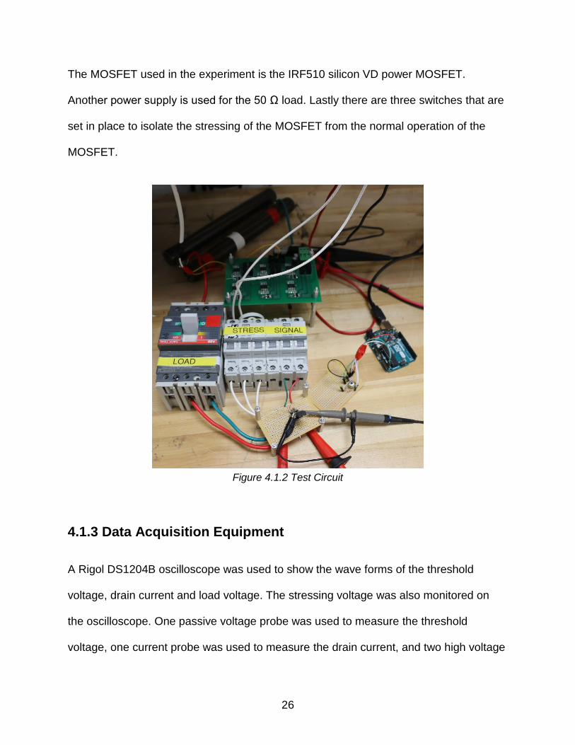
The pieces of equipment that were used for the test setup shown in figure 4.1.2. There
is one power supply needed to age the MOSFET and run the gate driver. A function
generator gives the pulse to the gate drive to drive the MOSFET. Next there is a gate
resistance added to more clearly see the threshold voltage during turn on and turn off.
Figure 4.1.1 Test Circuit Configuration
26
The MOSFET used in the experiment is the IRF510 silicon VD power MOSFET.
Another power supply is used for the 50 Ω load. Lastly there are three switches that are
set in place to isolate the stressing of the MOSFET from the normal operation of the
MOSFET.
4.1.3 Data Acquisition Equipment
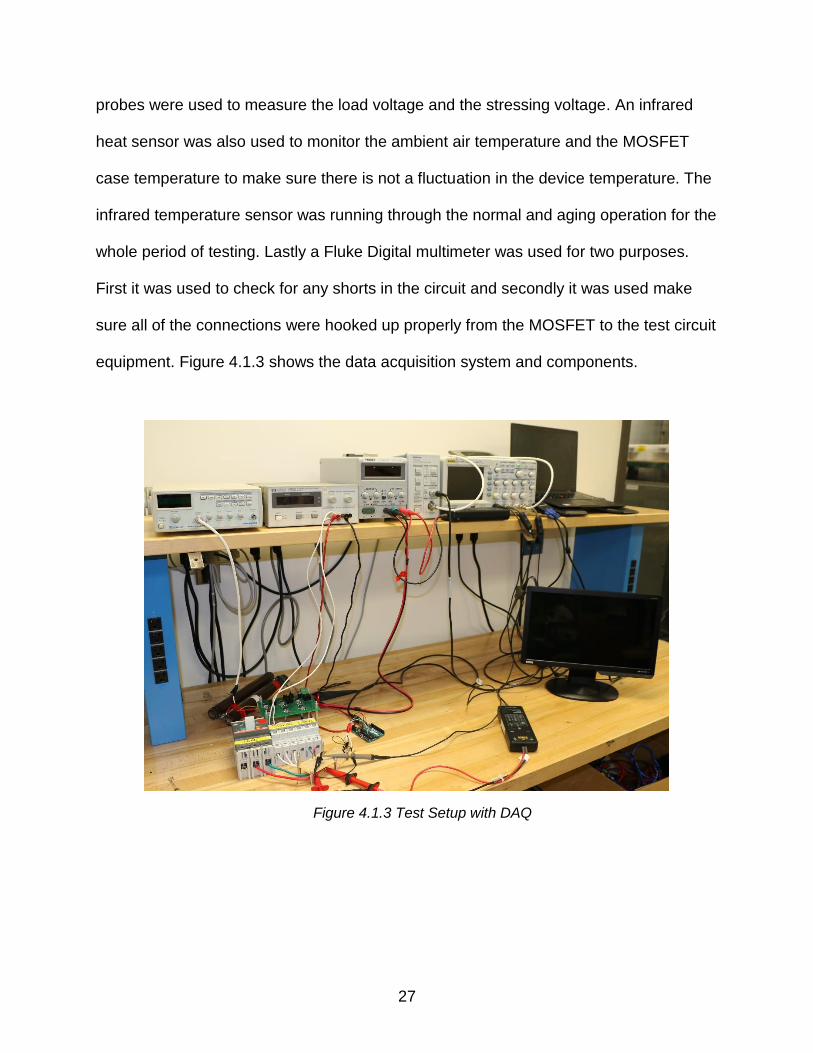
A Rigol DS1204B oscilloscope was used to show the wave forms of the threshold
voltage, drain current and load voltage. The stressing voltage was also monitored on
the oscilloscope. One passive voltage probe was used to measure the threshold
voltage, one current probe was used to measure the drain current, and two high voltage
Figure 4.1.2 Test Circuit
27
probes were used to measure the load voltage and the stressing voltage. An infrared
heat sensor was also used to monitor the ambient air temperature and the MOSFET
case temperature to make sure there is not a fluctuation in the device temperature. The
infrared temperature sensor was running through the normal and aging operation for the
whole period of testing. Lastly a Fluke Digital multimeter was used for two purposes.
First it was used to check for any shorts in the circuit and secondly it was used make
sure all of the connections were hooked up properly from the MOSFET to the test circuit
equipment. Figure 4.1.3 shows the data acquisition system and components.
Figure 4.1.3 Test Setup with DAQ

28
4.2 Test Procedure
4.2.1 Normal Operation of the Power MOSFET
The first procedure of the test circuit is run under normal operation. In order to run the
circuit under normal operation switch 3 should be opened to disconnect the stressing
circuit and switches 1 and 2 should be closed to have the gate drive and load
connected. Next, 24 V powered the gate drive and then the function generator will be
turned on to drive the gate drive from a high 10 V to a low -5 V at 1.7 kHz. These
voltage values were chosen from the MOSFET data sheet recommendations. The load
voltage supplied is 30 V and the load resistance is 50 Ω. The maximum load voltage
should not exceed 100 V so a lower voltage was chosen in order to concentrate the
aging of the MOSFET across the gate oxide. This way the drain to source was not
stressed and aged to a degree that it would change the results for the threshold voltage.
During this normal operation, the threshold voltage will be measured and recorded.
Figure 4.1.1 shows the normal operation of the circuit when switches 1 and 2 are
closed, and switch 3 is open. The threshold voltage was measured at the point in time
when the drain current started to conduct. The threshold voltage was measured this
way throughout the entire aging process for consistency.
4.2.2 Aging the Power MOSFET
In order to age the MOSFET a voltage stressing technique was used. For the aging
process to begin, the normal operation circuit must first be isolated from the stressing

29
circuit by opening switches 1 and 2, which are connected to the gate drive and the load
respectively. Next switch 3, which goes directly to the gate, drain, and source must be
closed for the stressing to begin. This circuit was setup for a high voltage to be applied
across the gate and source, with the source of the MOSFET shorted to the drain. Once
these connections are made sure of, the voltage will be turned up slowly, about 1 to 2
V/s to prevent immediate breakdowns within the gate oxide. In order to choose the
stressing voltage multiple MOSFETs were used to find a range of voltages
corresponding to how long they last before failure. First, three MOSFETs were tested to
see at which voltage level there was an immediate breakdown across the gate oxide.
Then, more MOSFETs were tested at various other high voltages to see how long it
takes for the device to fail. After these tests were completed, it was found that the
MOSFET should be stressed at around 65 V to induce accelerated aging of the gate
oxide. After running the test at 65.2 V it was found that this voltage was high enough to
age the MOSFET but also low enough to be able to plot the threshold voltage across
time. Figure 4.1.1 shows the stressing of the MOSFET by applying a constant 65.2 V
across the gate and source of the MOSFET with the drain shorted to the source.
4.2.3 Data Acquisition
In order to get measurements of the threshold voltage over a period of time the test
circuit must be switched back and forth from normal operation to the stressing circuit
throughout the entire process. Figure 4.2.3 shows how the process will be handled.
30
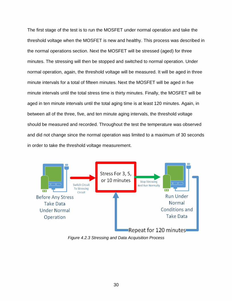
The first stage of the test is to run the MOSFET under normal operation and take the
threshold voltage when the MOSFET is new and healthy. This process was described in
the normal operations section. Next the MOSFET will be stressed (aged) for three
minutes. The stressing will then be stopped and switched to normal operation. Under
normal operation, again, the threshold voltage will be measured. It will be aged in three
minute intervals for a total of fifteen minutes. Next the MOSFET will be aged in five
minute intervals until the total stress time is thirty minutes. Finally, the MOSFET will be
aged in ten minute intervals until the total aging time is at least 120 minutes. Again, in
between all of the three, five, and ten minute aging intervals, the threshold voltage
should be measured and recorded. Throughout the test the temperature was observed
and did not change since the normal operation was limited to a maximum of 30 seconds
in order to take the threshold voltage measurement.
Figure 4.2.3 Stressing and Data Acquisition Process
31
4.3 Thermomechanical Stress Isolation from Electrical
Stresses
This test is setup so that the main focus is on the electrical stresses to the device rather
than both the thermomechanical and electrical stresses due to the aging process.
Thermomechanical stresses and electrical stresses were talked about in Chapter 2. In
this test as explained previously, the gate oxide breakdown of the MOSFET is the point
of focus for stressing the device. A voltage higher than the maximum rating of VGS was
applied to the MOSFET over periods of time ranging from three minutes to more than
three hours. During this stressing no temperature change was noticed in the device.
The temperature remained at room temperature which was 75 degrees Fahrenheit.
When the device was run under normal operation, with a load, the did not rise until
around 2 minutes of operation. Even then the temperature only rose up to around 78
degrees Fahrenheit. This small temperature fluctuation in the device will not cause any
of the mechanical failures such as bond-wire liftoff or bond-wire cracking. When running
the test, the operation time in normal operation with the load was limited to around 30
seconds to try and completely eliminate any temperature rise within the device. The
reason that in this test the different stresses were isolated from each other was to see
how the threshold voltage will change throughout its life without encountering
thermomechanical stresses. These thermomechanical stresses may change the
measurement of the threshold voltage due to heating up and or the breakage of bond-
wires. As the temperature rises, it is known that the threshold voltage decreases. This
32
change in threshold voltage is not what would like to be observed in this test. So in this
case isolation between the electrical and thermal stresses was set in place.
4.4 C-V Measurement
In this experiment one IRF510 MOSFET was used to measure the capacitance over the
aging cycle. This was used to see by how much the oxide had begun to degrade and
this tool was useful to see the shift in the threshold voltage. Measurements were taken
before any aging and in between each aging interval up to 20 minutes of aging. A graph
showing the trends of these findings can be seen in Chapter 5. This is a reliable method
to check and see if the threshold voltage measured during normal operation is accurate
with respect to the C-V measurement.
4.5 Annealing
In this experiment, one IRF510 MOSFET was annealed. This technique was used to
see what effects were causing the threshold voltage to shift. The device was annealed
at 120 C for about one hour after three minutes of aging. The threshold voltage shifted
back up from the drop that was experienced in this test. These results will be talked
about in more detail in Chapter 5. To anneal any device, the data sheet of that device
should be looked at in order to see what maximum temperature the device can handle.
Also when annealing a device, if the threshold voltage does not change this means that
33
a much higher temperature than what the device is rated for should be used because
the charges are trapped more than a few eV’s into the material.

34
Chapter 5
Evaluation of Test Data
This chapter will go into detail about the test results. First the data extracted from the
testing will be explained. There will be figures showing the trends of the threshold
voltage of the power MOSFETs. Two explanations will be given for the “dip and
rebound” concept. Finally, future work and conclusions will be given.
5.1 Test Data
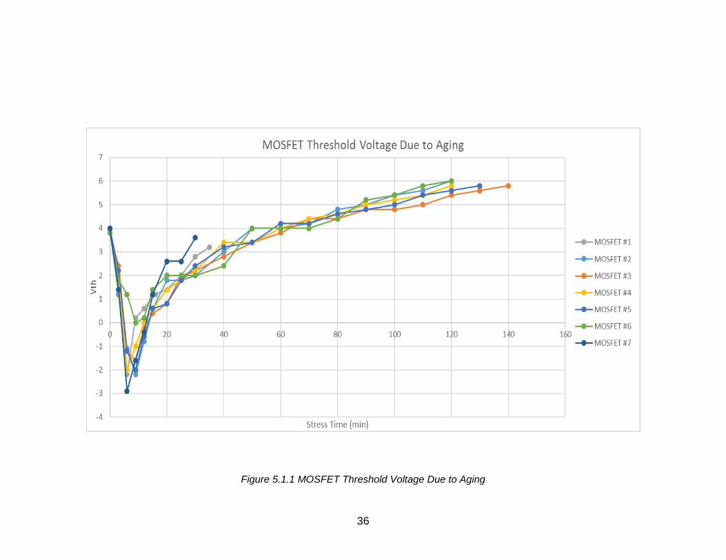
The threshold voltage of seven MOSFETs were measured to prove the theory of the
“dip and rebound” concept. As can be seen in Figure 5.1.1, all of the MOSFETs follow
the same pattern dipping in the beginning and then continuously rising as the aging
process proceeds. There are very few variations from MOSFET to MOSFET throughout
the test. All of these MOSFETs were tested at room temperature with no heating or
cooling of the device. An interesting phenomenon can be seen in the curve for the
MOSFET threshold voltage. After a short period of stressing, the threshold voltage
dropped to a negative value. In this case, the MOSFET that was being used is an n-
channel MOSFET. Therefore, throughout the whole operation in the negative region of
the threshold voltage means that the MOSFET was operating in the depletion mode.
The curve starts in the enhancement mode of the MOSFET, then dips into the depletion

35
mode, and finally rebounds back into the enhancement mode. It should be noted that
while in the depletion mode the MOSFET is “normally on” and needs to be turned off. In
Figure 5.1.1, the trend can be seen of the threshold voltage throughout the aging
process. Also in Figure 5.1.2, the C-V plot can be seen of one of the MOSFETs
stressed in the experiment.
36
Figure 5.1.1 MOSFET Threshold Voltage Due to Aging
37
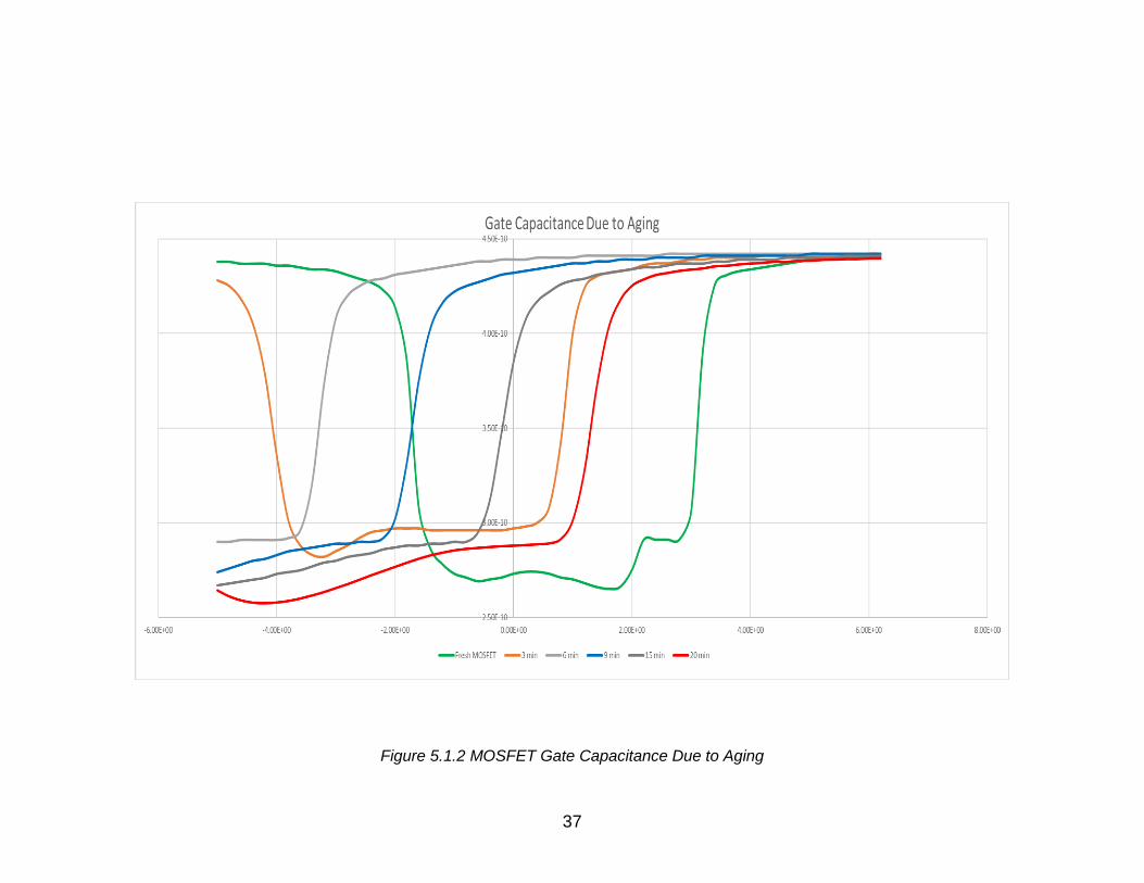
Figure 5.1.2 MOSFET Gate Capacitance Due to Aging
38
5.2 Critical Evaluation
5.2.1 Introduction
As stated in the theory description, a dip and rebound was seen in the threshold
voltage. Region I is shown to be the first measurements of the threshold voltage before
any aging has begun on the MOSFET. After the aging process has begun we move into
region II, where the dip begins. This dip was expected to happen near the beginning of
the aging process as shown from the experimental data gathered across multiple
MOSFETs. Although the dip was expected to occur, it was not expected to drop down
into the depletion mode. After noticing the dip into the negative voltage, the aging was
continued to determine if the threshold voltage would rebound. As expected the
threshold voltage did rebound, but from a negative voltage. This voltage then continued
to rise all the way above the max recommended range for the threshold voltage. Once a
two volt rise above the range was seen the aging was stopped with the MOSFETs still
functioning correctly. These MOSFETs were not aged until failure of the device because
the theory can be explained at the point where the MOSFETs were stopped in the aging
process. Each of the modes will be explained in more detail with respect to the
measurements taken during the experimental process. The dip into the depletion mode
will be explained with a modification of the theory. A fourth equation will be added
between the second and third modes of operation in the theory and the second equation
will also be modified. This entails that the second region of operation has two
contributing factors.
39
5.2.2 Evaluation with Respect to the Proposed Theory
Region I is a well-known topic. In this experiment the MOSFET was only run for 30
seconds to show a measurement in this region. This was done for such a short period
because during the MOSFETs life in region I everything is considered constant and
nothing should change in this region of operation. The second and third regions are
more important due to recognizing when the failure precursors start to initiate in the
power MOSFET. After aging for three minutes at 65.2 V, the threshold voltage was
measured and seen to have dropped approximately 1.4 V to 2 V. During this period, the
gate oxide has begun to degrade and breakdown. This was referred to as enhanced
bond breakage. It can be seen that this breakage in the Si-Si bonds has led to a
formation of traps and has created a localized conduction path in the gate oxide. So as
the oxide was thinning during the aging process, charge trapping was induced in the
material. Here holes are trapped because of the bond breakage. Interestingly, after
another three minutes of stressing, the n-channel enhancement mode power VD-
MOSFET turned into a depletion type MOSFET. The MOSFET remains as a depletion
type MOSFET as long as the threshold voltage value remains negative. Notably the
resistance up to this point between the drain and source kept dropping until the drain
and source terminals become shorted together. So as the threshold voltage dropped the
resistance across the drain and source followed respectively. At this point, the MOSFET
is normally on and needs to be turned off. It is highly unlikely that this is all due to only
the gate oxide degradation, which will be discussed in more detail in the next section
where what is believed to be the real cause behind this threshold voltage lowering
effect. Now, at this point in the aging process, the MOSFETs are operating in a region

40
they should not be. Operating the MOSFETs in the depletion region will have a much
higher power loss because the switch is conducting for a longer period of time.
Continuing into region II aging, the threshold voltage is continuing to drop for a short
period of time. The greatest change in the threshold voltage can be seen in Figure
5.1.1, which is a decrease of 6.9 V in MOSFET #7. After aging, as these MOSFETs
pass the six and nine minute marks, the MOSFETs start to come out of region II and
head into region III. In region III, Fowler-Nordheim tunneling begins to dominate and the
threshold voltage begins to rise. This does not mean that Fowler-Nordheim tunneling
did not start to occur previous to the six or nine minute mark of stressing, but rather, it
means that the trapped charges prior to this step were the dominating factor preceding
the rise of the threshold voltage. Now in region III, it is seen that for all MOSFETs the
threshold voltage keeps rising. As the threshold voltage rises it is seen that the
MOSFET again changed operating modes from a depletion type MOSFET to an
enhancement mode MOSFET again. Notably, the MOSFET operating mode changed in
order from enhancement to depletion and then back to enhancement. Aging was
stopped for each MOSFET when the threshold voltage reached a value close to 6 V.
Aging was stopped at this point because all three regions of operation were seen, and it
will be assumed that that the threshold voltage will keep rising till failure of the device.
The following is an alternative explanation that is more detailed and is the most
probable cause of the lowering of the threshold voltage.
41
5.2.3 Evaluation with Respect to the more Probable Solution
Region I, again, is the same in this explanation as it is with respect to the proposed
theory. It is assumed that there are no changes to the device so the threshold voltage
will stay the same in this region. The confusion belongs in region two. Here the
threshold voltage is dropping in the beginning stages of the aging process. It would
have been well off if the whole drop in the threshold voltage could be contributed to the
gate oxide degradation. As the gate oxide degrades, positive trapped charges are
formed in the oxide when the bonds between the silicon atoms. Holes can also be
transported through the oxide through radiation-induced oxide charge [24]. These
trapped charges may cause the threshold voltage to decrease depending on how many
traps have accumulated in the oxide. Also, the devices under the conditions they were
operated at will not experience the radiation induced charges. With that being said, the
amount of trapped positive charges in the oxide by themselves should not be able to
cause the threshold voltage to decrease into the negative region causing the MOSFET
to operate in the depletion mode without radiation-induced oxide charge. Radiation-
induced charges were not mentioned in the proposed theory. It is well known that most
of the positive trapping is at the interface of the substrate and the gate oxide. The gate
oxide usually only traps electrons since there is a positive bias being applied. Therefore
the amount of stress being applied to the MOSFETs has to be taken into consideration,
since it can cause adverse effects to the operation of the oxide and the substrates
inside the MOSFETs. In the IRF510PBF MOSFETs it is recommended to not exceed
positive or negative 20 V at the gate. When taking the measurements of the threshold
voltage these values were not exceeded. But while stressing the MOSFETs the positive
42
20 V was exceeded by over three times at 65.2 V. This is because an accelerated aging
test was used. Applying this high of a voltage stress can affect the way the p-body
substrate diffuses by decreasing the mobility in the body. The stress can also cause an
interface to form quicker which can cause a high buildup of interface traps in the
substrate between the gate oxide and the p-substrate. Another factor that can cause
these effects may be the body effect.
Diffusion of electrons and holes happens in the substrate of the MOSFET. When the
stress is applied to the gate, there is stress being applied to the substrate as well. Here,
is where the properties of the substrate can change and cause the mobility of the
electrons and holes to change. Also the dopant its self can move around due to the
stress being applied. This means the profile of the dopant in the P-base region was
changed or moved. What could also be happening in this VD-MOSFET is that the
mobility of the holes is slowing down, which can cause a buildup of holes in the
substrate of the material. This could then cause the device to a have a body type effect.
The electron mobility in this device is assumed to be higher than the hole mobility.
Since there are more holes, a lesser or more negative voltage is needed to turn the
device off. The holes that are being trapped can accumulate till the point where it
pushes the MOSFET into the depletion mode. As seen in the results, the MOSFET was
pushed into the depletion mode during operation in region II. In non-VD-MOSFETs, the
body effect is known to cause the threshold voltage to drop because it gets charged up
negatively and pushes the electrons toward the channel. This causes the bulk to have a
different potential than the source of the MOSFET, which causes the MOSFET to
normally stay on. Consequently, a negative voltage or a voltage lower than the source
43
potential of the MOSFET is needed in order to turn the MOSFET off. In the case of the
IRF510PBF, which is a VD-MOSFET, the source is shorted to the bulk of the MOSFET
which may mean this MOSFET will have a lesser body effect than described for the
non-VD-MOSFET case. The lowering of the threshold voltage can be seen because of
the trapped charges in the substrate, but the interface charges are believed to be the
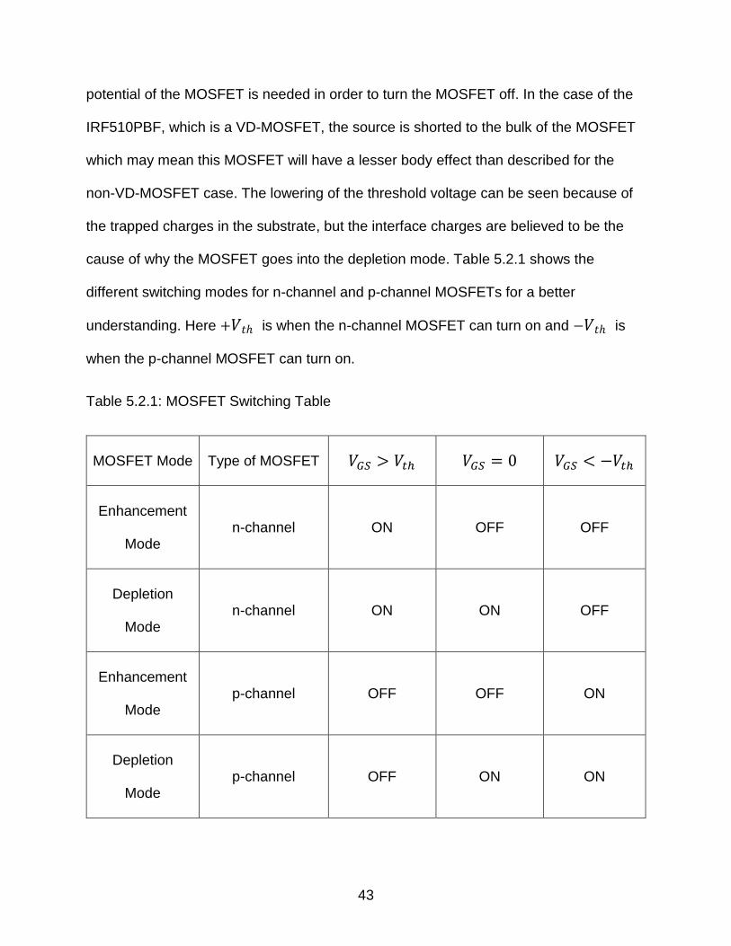
cause of why the MOSFET goes into the depletion mode. Table 5.2.1 shows the
different switching modes for n-channel and p-channel MOSFETs for a better
understanding. Here +𝑉𝑡ℎ is when the n-channel MOSFET can turn on and −𝑉𝑡ℎ is
when the p-channel MOSFET can turn on.
Table 5.2.1: MOSFET Switching Table
MOSFET Mode
Type of MOSFET 𝑉𝐺𝑆 > 𝑉𝑡ℎ 𝑉𝐺𝑆 = 0 𝑉𝐺𝑆 < −𝑉𝑡ℎ
Enhancement
Mode
n-channel
ON
OFF
OFF
Depletion
Mode
n-channel
ON
ON
OFF
Enhancement
Mode
p-channel
OFF
OFF
ON
Depletion
Mode
p-channel
OFF
ON
ON
44
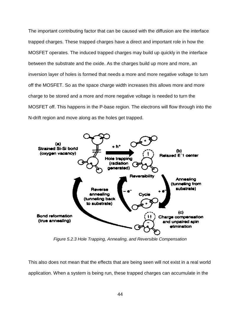
The important contributing factor that can be caused with the diffusion are the interface
trapped charges. These trapped charges have a direct and important role in how the
MOSFET operates. The induced trapped charges may build up quickly in the interface
between the substrate and the oxide. As the charges build up more and more, an
inversion layer of holes is formed that needs a more and more negative voltage to turn
off the MOSFET. So as the space charge width increases this allows more and more
charge to be stored and a more and more negative voltage is needed to turn the
MOSFET off. This happens in the P-base region. The electrons will flow through into the
N-drift region and move along as the holes get trapped.
This also does not mean that the effects that are being seen will not exist in a real world
application. When a system is being run, these trapped charges can accumulate in the
Figure 5.2.3 Hole Trapping, Annealing, and Reversible Compensation
45
gate oxide, interface, and the substrate. If the MOSFETs are held at room temperature
the user will start to see a drop in the threshold voltage. Now if the user wants to get rid
of the trapped charges, they may anneal the MOSFET and see that the charges are
now free and have recombined. There are charges that are permanent that may seem
to go away with the annealing of the device only to reappear and cause a negative shift
in the threshold as found in [25]. Also, the interface state trapped charges can
repopulate causing the threshold voltage to shift again. The model for hole trapping,
annealing, and reversible compensation is shown in figure 5.2.3 [25].
Here, it can be noted that the permanent trapped charges that reappear to cause the
threshold voltage shift are holes permanently trapped in the gate oxide. Also the
interface will begin to repopulate with charges during normal operation. This is because
the charges were imbedded into the material, which leaves states for the charges to be
trapped again after they are thermally excited out of the trapped states. It will be difficult
to see the voltage shift due to oxide trapped charges. This is because the interface
trapped charges and the charges in the P-body will begin to reappear. These charges
will shift the threshold voltage more than the oxide trapped charges will. In the end, real
systems can experience the shift from an enhancement type MOSFET to a depletion
mode and then back to an enhancement type MOSFET.
When the device’s threshold voltage begins to rebound and come back up, Fowler-
Nordheim tunneling begins to dominate. Again as in the first explanation, Fowler-
Nordheim tunneling may begin to occur previous to the voltage rebound but does not
have an overwhelming effect. It is again assumed that the threshold voltage will
46
continue to rise even though the testing and stressing was stopped about two hours into
the lifetime of the MOSFET.
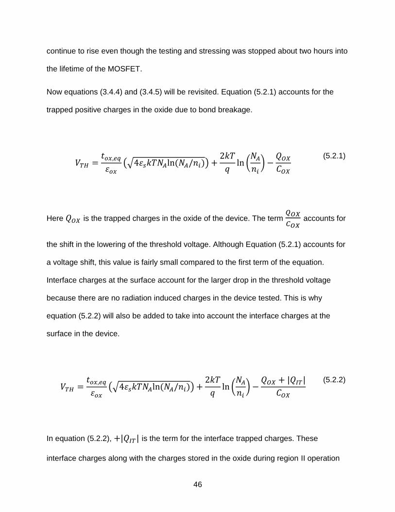
Now equations (3.4.4) and (3.4.5) will be revisited. Equation (5.2.1) accounts for the
trapped positive charges in the oxide due to bond breakage.
𝑉𝑇𝐻 =𝑡𝑜𝑥,𝑒𝑞𝜀𝑜𝑥
(√4𝜀𝑠𝑘𝑇𝑁𝐴ln(𝑁𝐴/𝑛𝑖)) +2𝑘𝑇
𝑞ln (
𝑁𝐴𝑛𝑖) −
𝑄𝑂𝑋𝐶𝑂𝑋
(5.2.1)
Here 𝑄𝑂𝑋 is the trapped charges in the oxide of the device. The term 𝑄𝑂𝑋
𝐶𝑂𝑋 accounts for
the shift in the lowering of the threshold voltage. Although Equation (5.2.1) accounts for
a voltage shift, this value is fairly small compared to the first term of the equation.
Interface charges at the surface account for the larger drop in the threshold voltage
because there are no radiation induced charges in the device tested. This is why
equation (5.2.2) will also be added to take into account the interface charges at the
surface in the device.
𝑉𝑇𝐻 =𝑡𝑜𝑥,𝑒𝑞𝜀𝑜𝑥
(√4𝜀𝑠𝑘𝑇𝑁𝐴ln(𝑁𝐴/𝑛𝑖)) +2𝑘𝑇
𝑞ln (
𝑁𝐴𝑛𝑖) −
𝑄𝑂𝑋 + |𝑄𝐼𝑇|
𝐶𝑂𝑋
(5.2.2)
In equation (5.2.2), +|𝑄𝐼𝑇| is the term for the interface trapped charges. These
interface charges along with the charges stored in the oxide during region II operation

47
will cause the threshold voltage to drop to a negative value which will cause the
enhancement device to begin operating as a depletion type device. The interface
trapped charges will form previous to any degradation in the gate oxide. When Fowler-
Nordheim tunneling begins to dominate and the threshold voltage goes above the
healthy state threshold voltage of the device, the term −𝑄𝑂𝑋+|𝑄𝐼𝑇|
𝐶𝑂𝑋 can be taken out
of the equation. However, before this happens Equation (3.4.5) which accounts for the
trapped positive charges must be modified into Equation (5.2.3).
𝑉𝑇𝐻 =𝑡𝑜𝑥,𝑒𝑞𝜀𝑜𝑥
(√4𝜀𝑠𝑘𝑇𝑁𝐴ln(𝑁𝐴/𝑛𝑖)) +2𝑘𝑇
𝑞ln (
𝑁𝐴𝑛𝑖) −
𝑄𝑂𝑋 + |𝑄𝐼𝑇|
𝐶𝑂𝑋
+𝑄𝑡𝑟𝑎𝑝𝐶𝑜𝑥
(5.2.3)
In Equation 5.2.3, the electron charges begin to cancel out the trapped hole charges in
the oxide and interface. So this is where region III operation begins. Once Fowler-
Nordheim tunneling starts to dominate and control the threshold voltage, the equation
can be formed back into equation (3.4.5). This because now the electrons are
dominating the change in threshold voltage which is causing a higher and higher or
more positive threshold voltage needed to turn the device on. At the point when the
threshold voltage reaches a value greater than the region I threshold the term
−𝑄𝑂𝑋+|𝑄𝐼𝑇|
𝐶𝑂𝑋 can be disregarded. This means that Equations (5.2.1) and (5.2.2)
48
account for when the dip in the threshold voltage starts to the lowest negative threshold
value. Equation (5.2.3) describes when the threshold voltage begins to rebound. In this
equation, the trapped holes must still be accounted for since the device is still operating
as a depletion type MOSFET and or the threshold voltage is still lower than the first
threshold value in region I. After the threshold voltage rises above the first threshold
value, Equation (3.4.5) should be used.
The proposed theory has been disproven now that all three regions have been
accounted for and explained properly. The equations were revisited and altered in order
to account for the trapping which occurs in the interface and the gate oxide. This cannot
be directly proven with the data compiled but it is one explanation which is very
probable to happen. Additional testing should be done to try and fully prove the newly
proposed equations.
5.3 Future Work
Many more tests can be performed in order to fully extract the different causes in the
threshold voltage shift. One test that should be performed is a finite element analysis
(FEA) simulation. When carrying out this simulation, all the parameters from the doping
concentrations to the thicknesses and capacitances of the device need to be known.
Using FEA, the user should be able to predict how the device should react to different
forces placed on the device. The mechanical forces on the device that should be
monitored carefully are the heating and cooling of the materials. The electrical forces on
the device that should be monitored are the continuous over gate voltage for stressing
49
and the gate current when switching the device on and off. Using FEA the user should
be able to recreate the testing platform in the real-world and compare the results of
charge trapping and threshold voltage variation. This may better help and explain the
results that are being seen in the IRF510 testing.
Another test that should be performed is stressing the MOSFET in a thermal chamber at
various temperatures including room temperature. Stressing the device at a lower
voltage throughout the temperature ranges should be performed because the device
may react differently and charges may not be stored at concentrations as seen at the
65.2 V and at room temperature. The user should be able to see a threshold voltage
shift that will differ from what is being seen at room temperature. An assessment of how
the device reacts at over 110° C should also be performed. The observation may point
out new findings of which trapped charges will be permanently stored in the interface
and in the gate oxide. The ideal case at the higher temperature would be to see minimal
charge trapping in the interface and a higher concentration of permanently trapped
charges in the gate oxide. When a device in annealed, it should get rid of trapped
charges in the device and can hide permanent trapped charges for a period of time
also. These charges should reappear in the device. More research of how long
permanent trapped charges take to reappear should also be evaluated. Finally, an
assessment of how the threshold voltage reacts at below 0° C should also be
performed. This data should be collected at different temperatures so that the threshold
voltage of the device can be compared and evaluated. The user should then see how
trapped charges affect the device at different temperatures. Combining FEA with the
50
thermal chamber testing would be the best scenario to provide the most accurate
understanding about what is going on in the MOSFET.
5.4 Conclusion
The power VD-MOSFET goes through three regions of operation. Region I being where
no change occurs in the MOSFET and the threshold voltage remains constant. The
second region of operation is when two different positive trapping methods occur, oxide
trapping and interface trapping. The third region of operation is where Fowler-Nordheim
tunneling begins to dominate the change in threshold voltage. In region II Fowler-
Nordheim tunneling was present but did not play the dominant role. Equation (3.4.4)
was to show the dip in the threshold voltage and (3.4.5) is for region III operation where
Fowler-Nordheim tunneling begins to dominate. These equations were altered in order
to compensate for the positive trapped charges during the dip in the threshold voltage
and when the threshold voltage begins rising in region III. Equations (5.2.1), (5.2.2), and
(5.2.3) is the result that can be seen. For the latter part of region III, when Fowler-
Nordheim tunneling dominates and the threshold value rises above the first value
recorded equation (3.4.5) will kept the same. Further analytical experimental simulations
using FEA are noted to be performed for a better understanding of what is going on in
the substrates and oxide of the MOSFET. Also, thermal chamber testing and annealing
are proposed to gain a stronger backing for the newly proposed equations. These
equations may be used for other devices such as IGBTs, SiC, and GaN MOSFETs.
Before using the equations for other devices, the device must first be tested and a
51
similar curve to the VD-MOSFET for the threshold voltage must be seen. Also, during
the accelerated aging test, data was collected to calculate the turn on resistance
concurrently with the threshold voltage of the MOSFET. These findings for the turn on
resistance along with the threshold voltage findings will be published at a later date.

52
BIBLIOGRAPHY
53
BIBLIOGRAPHY
[1] Vichare, N.M.; Pecht, M.G., "Prognostics and health management of electronics," Components and Packaging Technologies, IEEE Transactions on , vol.29, no.1, pp.222,229, March 2006. [2] Anderson, J.M.; Cox, R.W., "On-line condition monitoring for MOSFET and IGBT switches in digitally controlled drives," Energy Conversion Congress and Exposition (ECCE), 2011 IEEE , vol., no., pp.3920,3927, 17-22 Sept. 2011. [3] Nasrin, M.S.; Khan, F.H., "Characterization of aging process in power converters using spread spectrum time domain reflectometry," Energy Conversion Congress and Exposition (ECCE), 2012 IEEE , vol., no., pp.2142,2148, 15-20 Sept. 2012. [4] Saha, S.; Celaya, J.R.; Vashchenko, V.; Mahiuddin, S.; Goebel, K.F., "Accelerated aging with electrical overstress and prognostics for power MOSFETs," Energytech, 2011 IEEE, vol., no., pp.1,6, 25-26 May 2011. [5] N. Stojadinovic, I. Manic, V. Davidovic, D. Dankovic, S. Djoric-Veljkovic, S. Golubovic, S. Dimitrijev, “Effects of electrical stressing in power VDMOSFETs”, Microelectronics Reliability, Volume 45, Issue 1, January 2005, Pages 115-122. [6] R. Habchi, C. Salame, R. El Bitar, P. Mialhe,“Switching times variation of MOSFET devices with temperature and high-field stress,” Microelectronics Journal, Volume 39, Issue 5, May 2008, Pages 828- 831. [7] Celaya, J.R.; Saxena, A.; Kulkarni, C.S.; Saha, S.; Goebel, K., "Prognostics approach for power MOSFET under thermal-stress aging," Reliability and Maintainability Symposium (RAMS), 2012 Proceedings - Annual , vol., no., pp.1,6, 23-26 Jan. 2012. [8] Baliga, B. (2008). Fundamentals of Power Semiconductor Devices, Springer-Verlag,pp. 280-499. [9] Lenzlinger, M. and Snow E.H., “Fowler Nordheim Tunneling into Thermally Grown SiO2,” Journal of Applied Physics, 40, 278-283 (1969). [10] McPherson, J. W. and Reddy, V. K. and Mogul, H. C.,“Field-enhanced Si–Si bond-breakage mechanism for time-dependent dielectric breakdown in thin-film SiO2 dielectrics,” Applied Physics Letters,” 71, 1101-1103 (1997). [11] Chenming Hu; Qiang Lu, "A unified gate oxide reliability model," Reliability Physics Symposium Proceedings, 1999. 37th Annual. 1999 IEEE International , vol., no., pp.47,51, 1999.
54
[12] Udo Schwalke, Martin Pölzl, Thomas Sekinger, Martin Kerber, Ultrathick gate oxides: charge generation and its impact on reliability, Microelectronics Reliability, Volume 41, Issue 7, July 2001, Pages 1007-1010. [13] Tewksbury, T.L., III; Lee, H.-S., "Characterization, modeling and minimization of transient threshold voltage shifts in MOSFETs," Custom Integrated Circuits Conference, 1993., Proceedings of the IEEE 1993 , vol., no., pp.14.4.1,14.4.4, 9-12 May 1993. [14] J. W. Mcpherson (2002), “Physics and chemistry of intrinsic timedependent dielectric breakdown in Sio2 dielectrics”, Book: Oxide Reliability: pp. 135-171, 2002. [15] Ku, P.S.; Schroder, D.K., "Charges trapped throughout the oxide and their impact on the Fowler-Nordheim current in MOS devices," Electron Devices, IEEE Transactions on , vol.41, no.9, pp.1669,1672, Sep 1994. [16] T. C. Yang and K. C. Saraswat, “Effect of physical stress on the degradation of thin SiO2 films under electrical stress,” IEEE Trans. Electron Devices, vol. 47, no. 4, pp. 746–755, Apr. 2000. [17] Bottini, R.; Sebastiani, A.; Galbiati, N.; Scozzari, C.; Ghidini, G., "Oxide Reliability: a new Methodology for Reliability Evaluation at Parametric Testing," Integrated Reliability Workshop Final Report, 2006 IEEE International, vol., no., pp.142,145. [18] Mong-Song Liang; Chi Chang; Yew Tong Yeow; Chenming Hu; Brodersen, R.W., "MOSFET degradation due to stressing of thin oxide," Electron Devices, IEEE Transactions on , vol.31, no.9, pp.1238,1244. [19] Y. Xiong, X. Cheng, Z. J. Shen, C. Mi, H. Wu and V. K. Garg, "Prognostic and Warning System for Power-Electronic Modules in Electric, Hybrid Electric, and Fuel-Cell Vehicles," in IEEE Transactions on Industrial Electronics, vol. 55, no. 6, pp. 2268-2276, June 2008. [20] H. K. Tseng and M. L. Wu, "Electro-thermal-mechanical modeling of wire bonding failures in IGBT," 2013 8th International Microsystems, Packaging, Assembly and Circuits Technology Conference (IMPACT), Taipei, 2013, pp. 152-157. [21] Z. Sarkany, A. Vass-Varnai and M. Rencz, "Investigation of die-attach degradation using power cycling tests," 2013 IEEE 15th Electronics Packaging Technology Conference (EPTC 2013), Singapore, 2013, pp. 780-784. [22] Celaya, J., A. Saxena, P. Wysocki, S. Saha, and K. Goebel. "Towards Prognostics of Power MOSFETs: Accelerated Aging and Precursors of Failure". in Annual Conference of the Prognostics and Health Management Society 2010. [23] G Timp, J Bude, F Baumann, K.K Bourdelle, T Boone, J Garno, A Ghetti, M Green, H Gossmann, Y Kim, R Kleiman, A Kornblit, F Klemens, S Moccio, D Muller, J Rosamilia,
55
P Silverman, T Sorsch, W Timp, D Tennant, R Tung, B Weir, The relentless march of the MOSFET gate oxide thickness to zero, Microelectronics Reliability, Volume 40, Issues 4–5, 1 April 2000, Pages 557-562 [24] Neamen, D. A. (2012). Semiconductor physics and devices: Basic principles. New York, NY: McGraw-Hill. [25] T. R. Oldham, "Switching oxide traps" in Radiation Effects and Soft Errors in Integrated Circuits and Electronic Devices, 2004, World Scientific.