Embed Size (px)
Citation preview
http://go.warwick.ac.uk/lib-publications
Original citation: Gammon, P. M., Donchev, E., Perez Tomas, A., Shah, V. A., Pang, J. S., Petrov, P.K., Jennings, M. R., Fisher, C. A., Mawby, P. A. (Philip A.), Leadley, D. R. (David R.) and Alford, N. McN. (2012) A study of temperature-related non-linearity at the metal-silicon interface. Journal of Applied Physics, Vol.112 . Article no. 114513 Permanent WRAP url: http://wrap.warwick.ac.uk/52407 Copyright and reuse: The Warwick Research Archive Portal (WRAP) makes the work of researchers of the University of Warwick available open access under the following conditions. Copyright © and all moral rights to the version of the paper presented here belong to the individual author(s) and/or other copyright owners. To the extent reasonable and practicable the material made available in WRAP has been checked for eligibility before being made available. Copies of full items can be used for personal research or study, educational, or not-for-profit purposes without prior permission or charge. Provided that the authors, title and full bibliographic details are credited, a hyperlink and/or URL is given for the original metadata page and the content is not changed in any way. Publisher’s statement: © (2012) American Institute of Physics. This article may be downloaded for personal use only. Any other use requires prior permission of the author and the American Institute of Physics. The following article appeared in Gammon, P. M., et al. (2012). A study of temperature-related non-linearity at the metal-silicon interface. Journal of Applied Physics, Vol.112 . Article no. 114513 and may be found at http://link.aip.org/link/doi/10.1063/1.4768718 A note on versions: The version presented here may differ from the published version or, version of record, if you wish to cite this item you are advised to consult the publisher’s version. Please see the ‘permanent WRAP url’ above for details on accessing the published version and note that access may require a subscription. For more information, please contact the WRAP Team at: [email protected]
A study of temperature-related non-linearity at the metal-silicon interface.
A study of temperature-related non-linearity at the metal-silicon interface.P. M. Gammon,1, 2, 3 E. Donchev,2 A. Perez-Tomas,4 V. A. Shah,3 J. S. Pang,2 P. K. Petrov,2 M. R. Jennings,1
C. A. Fisher,1 P. A. Mawby,1 D. R. Leadley,3 and N. McN. Alford2
1)School of Engineering, University of Warwick, Coventry, CV4 7AL, United Kingdom2)Department of Materials, Imperial College London, London, SW7 2AZ, United Kingdom3)Physics Department, University of Warwick, Coventry, CV4 7AL, United Kingdom4)IMB-CNM-CSIC, Campus UAB, 08193 Barcelona, Spain
(Dated: 2 January 2013)
In this paper, we investigate the temperature dependencies of metal-semiconductor interfaces in an effort tobetter reproduce the current-voltage-temperature (I-V-T) characteristics of any Schottky diode, regardlessof homogeneity. Four silicon Schottky diodes were fabricated for this work, each displaying different degreesof inhomogeneity; a relatively homogeneous NiV/Si diode, a Ti/Si and Cr/Si diode with double bumps atonly the lowest temperatures, and a Nb/Si diode displaying extensive non-linearity. The 77-300 K I-V-Tresponses are modelled using a semi-automated implementation of Tung’s electron transport model, and eachof the diodes are well reproduced. However, in achieving this, it is revealed that each of the three key fittingparameters within the model display a significant temperature dependency. In analysing these dependencies,we reveal how a rise in thermal energy “activates” exponentially more interfacial patches, the activationrate being dependent on the carrier concentration at the patch saddle point (the patch’s maximum barrierheight), which in turn is linked to the relative homogeneity of each diode. Finally, in a review of Tung’smodel, problems in the divergence of the current paths at low temperature are explained to be inherent dueto the simplification of an interface that will contain competing defects and inhomogeneities.
PACS numbers: Valid PACS appear hereKeywords: Suggested keywords
I. INTRODUCTION
Schottky barriers, formed at the interface between ametal and a low-doped semiconductor, are the simplestof electronic phenomena and occur in numerous devices.Most obvious is the Schottky diode which, comparedwith a semiconductor-semiconductor diode such as a PiNdiode, has very fast switching speeds and low turn-onvoltages due to its reliance only on majority carrier trans-port, free of the recombination mechanism. This makesthe Schottky diode a popular choice in applications suchas switched mode power supplies, RF, voltage clamping,and now extensively also in power electronics, where thelatest silicon carbide (SiC) Schottky diodes from Creeare capable of blocking voltages up to 1700 V1. Schottkybarriers also find use as the gate of high electron mo-bility transistors (HEMT), where one of the most popu-lar combinations is AlGaN/GaN, with the Schottky bar-rier being formed to the GaN top layer2–4, though manyother III-V combinations have been suggested5. Otherapplications include carbon nanotube Schottky barriertransistors6, and Schottky solar cells, with materials in-cluding lead selenide nanocrystals7 and graphene8.
Despite over a hundred years of research and devel-opment into Schottky barriers, across all popular semi-conductors and for the various applications, we still findourselves with unanswered questions as to the nature ofcurrent flow across the barrier, especially in light of in-homogeneity at the metal-semiconductor interface9,11–24,which can result in multiple conduction paths throughthe non-uniform interface. Sources of interfacial inho-mogeneity include processing remnants (dirt, contamina-
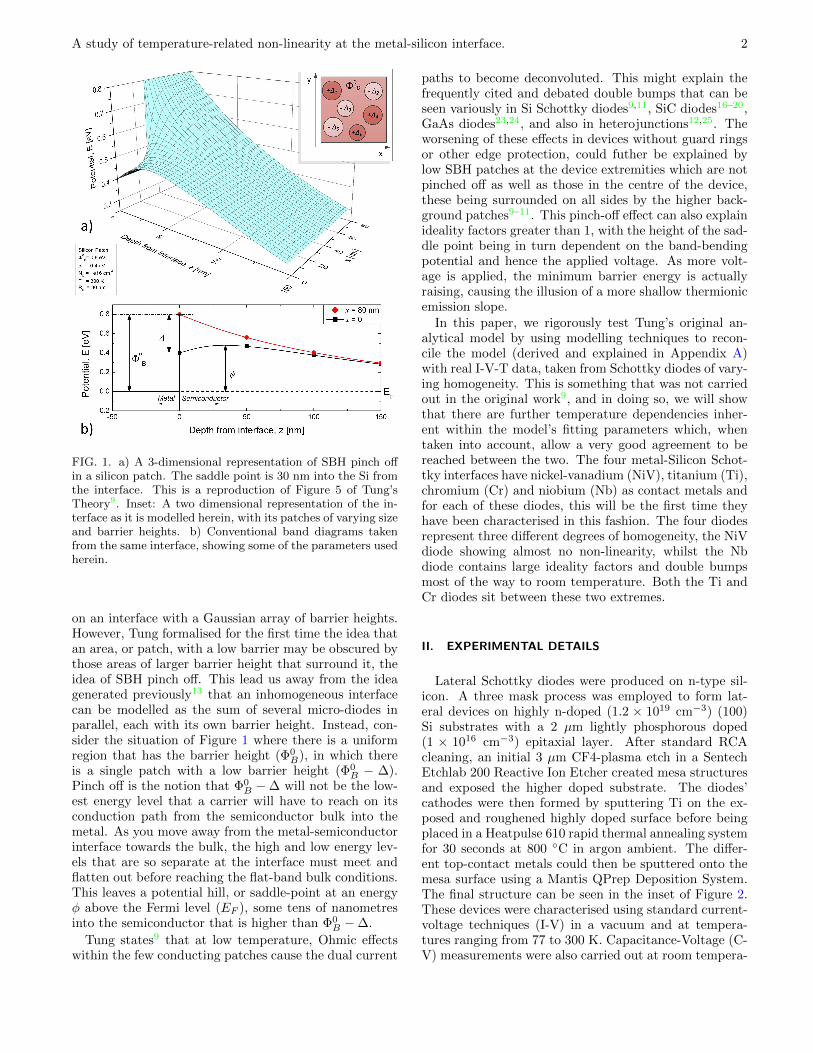
tion), surface roughness, native oxide, an uneven dopingprofile, crystal defects and grain boundaries9,11,12 and itis generally now accepted that the surface is better rep-resented as a random array of different patches, each ofvarying barrier height and area, as represented in theinset of Figure 1a.
The thermionic emission equation has long since beenused to model the turn-on characteristics of Schottkydiodes, and predicts that as a diode turns on, it will havea linear response on a semi-log plot with an ideality fac-tor, η, approaching 1. The thermionic emission equationis,
I = AA∗T 2 exp (−βΦ) [exp (βVA/η)− 1] , (1)
where A represents the contact area, A∗ is the Richard-son constant, T is the temperature, Φ is the Schottkybarrier height, VA is the applied voltage and β = q/kbT ,with q the electron charge, and kb the Boltzmann con-stant. Interfacial inhomogeneity has been cited9–24 asthe cause for many experimental results that deviatefrom this response. These so called non-linearities in-clude high ideality factors9,11,13, the discrepancy betweenSchottky barrier heights (SBH) extracted via CV and IVtechniques9–15, the “T0 anomaly”9,11,13, double bumpswithin the semi-log turn-on characteristics9,11,13,16–20,edge effects9,11 and non-linearity within Richardsonplots22.
It was the papers written by Tung9–11 however, thatfirst introduced a model that adapted Equation 1 to fullyexplain the non-linearities in light of interfacial inhomo-geneity and SBH fluctuation. Tung built on the work ofthose that had proceeded him13–15 by basing his model
A study of temperature-related non-linearity at the metal-silicon interface. 2
FIG. 1. a) A 3-dimensional representation of SBH pinch offin a silicon patch. The saddle point is 30 nm into the Si fromthe interface. This is a reproduction of Figure 5 of Tung’sTheory9. Inset: A two dimensional representation of the in-terface as it is modelled herein, with its patches of varying sizeand barrier heights. b) Conventional band diagrams takenfrom the same interface, showing some of the parameters usedherein.
on an interface with a Gaussian array of barrier heights.However, Tung formalised for the first time the idea thatan area, or patch, with a low barrier may be obscured bythose areas of larger barrier height that surround it, theidea of SBH pinch off. This lead us away from the ideagenerated previously13 that an inhomogeneous interfacecan be modelled as the sum of several micro-diodes inparallel, each with its own barrier height. Instead, con-sider the situation of Figure 1 where there is a uniformregion that has the barrier height (Φ0
B), in which thereis a single patch with a low barrier height (Φ0
B − ∆).Pinch off is the notion that Φ0
B −∆ will not be the low-est energy level that a carrier will have to reach on itsconduction path from the semiconductor bulk into themetal. As you move away from the metal-semiconductorinterface towards the bulk, the high and low energy lev-els that are so separate at the interface must meet andflatten out before reaching the flat-band bulk conditions.This leaves a potential hill, or saddle-point at an energyφ above the Fermi level (EF ), some tens of nanometresinto the semiconductor that is higher than Φ0
B −∆.
Tung states9 that at low temperature, Ohmic effectswithin the few conducting patches cause the dual current
paths to become deconvoluted. This might explain thefrequently cited and debated double bumps that can beseen variously in Si Schottky diodes9,11, SiC diodes16–20,GaAs diodes23,24, and also in heterojunctions12,25. Theworsening of these effects in devices without guard ringsor other edge protection, could futher be explained bylow SBH patches at the device extremities which are notpinched off as well as those in the centre of the device,these being surrounded on all sides by the higher back-ground patches9–11. This pinch-off effect can also explainideality factors greater than 1, with the height of the sad-dle point being in turn dependent on the band-bendingpotential and hence the applied voltage. As more volt-age is applied, the minimum barrier energy is actuallyraising, causing the illusion of a more shallow thermionicemission slope.
In this paper, we rigorously test Tung’s original an-alytical model by using modelling techniques to recon-cile the model (derived and explained in Appendix A)with real I-V-T data, taken from Schottky diodes of vary-ing homogeneity. This is something that was not carriedout in the original work9, and in doing so, we will showthat there are further temperature dependencies inher-ent within the model’s fitting parameters which, whentaken into account, allow a very good agreement to bereached between the two. The four metal-Silicon Schot-tky interfaces have nickel-vanadium (NiV), titanium (Ti),chromium (Cr) and niobium (Nb) as contact metals andfor each of these diodes, this will be the first time theyhave been characterised in this fashion. The four diodesrepresent three different degrees of homogeneity, the NiVdiode showing almost no non-linearity, whilst the Nbdiode contains large ideality factors and double bumpsmost of the way to room temperature. Both the Ti andCr diodes sit between these two extremes.
II. EXPERIMENTAL DETAILS
Lateral Schottky diodes were produced on n-type sil-icon. A three mask process was employed to form lat-eral devices on highly n-doped (1.2 × 1019 cm−3) (100)Si substrates with a 2 µm lightly phosphorous doped(1 × 1016 cm−3) epitaxial layer. After standard RCAcleaning, an initial 3 µm CF4-plasma etch in a SentechEtchlab 200 Reactive Ion Etcher created mesa structuresand exposed the higher doped substrate. The diodes’cathodes were then formed by sputtering Ti on the ex-posed and roughened highly doped surface before beingplaced in a Heatpulse 610 rapid thermal annealing systemfor 30 seconds at 800 ◦C in argon ambient. The differ-ent top-contact metals could then be sputtered onto themesa surface using a Mantis QPrep Deposition System.The final structure can be seen in the inset of Figure 2.These devices were characterised using standard current-voltage techniques (I-V) in a vacuum and at tempera-tures ranging from 77 to 300 K. Capacitance-Voltage (C-V) measurements were also carried out at room tempera-
A study of temperature-related non-linearity at the metal-silicon interface. 3
ture. Lateral devices were formed to make wire bondingto these structures easier when it came to IVT testing.As seen in the inset of Figure 2, the mesa etch accuratelydefines the drift region between the metal and the homo-junction. On the application of a negative voltage (to amaximum of -5 V for the C-V measurements), the deple-tion region will never exceed the width of the drift region,so the devices are presumed to operate in the same fash-ion as conventional vertical devices for both CV and IVanalysis.
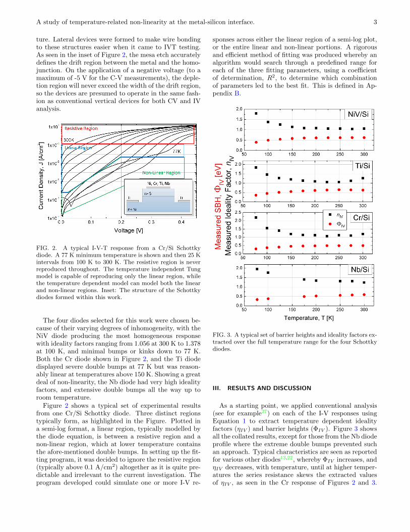
FIG. 2. A typical I-V-T response from a Cr/Si Schottkydiode. A 77 K minimum temperature is shown and then 25 Kintervals from 100 K to 300 K. The resistive region is neverreproduced throughout. The temperature independent Tungmodel is capable of reproducing only the linear region, whilethe temperature dependent model can model both the linearand non-linear regions. Inset: The structure of the Schottkydiodes formed within this work.
The four diodes selected for this work were chosen be-cause of their varying degrees of inhomogeneity, with theNiV diode producing the most homogeneous responsewith ideality factors ranging from 1.056 at 300 K to 1.378at 100 K, and minimal bumps or kinks down to 77 K.Both the Cr diode shown in Figure 2, and the Ti diodedisplayed severe double bumps at 77 K but was reason-ably linear at temperatures above 150 K. Showing a greatdeal of non-linearity, the Nb diode had very high idealityfactors, and extensive double bumps all the way up toroom temperature.
Figure 2 shows a typical set of experimental resultsfrom one Cr/Si Schottky diode. Three distinct regionstypically form, as highlighted in the Figure. Plotted ina semi-log format, a linear region, typically modelled bythe diode equation, is between a resistive region and anon-linear region, which at lower temperature containsthe afore-mentioned double bumps. In setting up the fit-ting program, it was decided to ignore the resistive region(typically above 0.1 A/cm2) altogether as it is quite pre-dictable and irrelevant to the current investigation. Theprogram developed could simulate one or more I-V re-
sponses across either the linear region of a semi-log plot,or the entire linear and non-linear portions. A rigorousand efficient method of fitting was produced whereby analgorithm would search through a predefined range foreach of the three fitting parameters, using a coefficientof determination, R2, to determine which combinationof parameters led to the best fit. This is defined in Ap-pendix B.
FIG. 3. A typical set of barrier heights and ideality factors ex-tracted over the full temperature range for the four Schottkydiodes.
III. RESULTS AND DISCUSSION
As a starting point, we applied conventional analysis(see for example27) on each of the I-V responses usingEquation 1 to extract temperature dependent idealityfactors (ηIV ) and barrier heights (ΦIV ). Figure 3 showsall the collated results, except for those from the Nb diodeprofile where the extreme double bumps prevented suchan approach. Typical characteristics are seen as reportedfor various other diodes13,22, whereby ΦIV increases, andηIV decreases, with temperature, until at higher temper-atures the series resistance skews the extracted valuesof ηIV , as seen in the Cr response of Figures 2 and 3.
A study of temperature-related non-linearity at the metal-silicon interface. 4
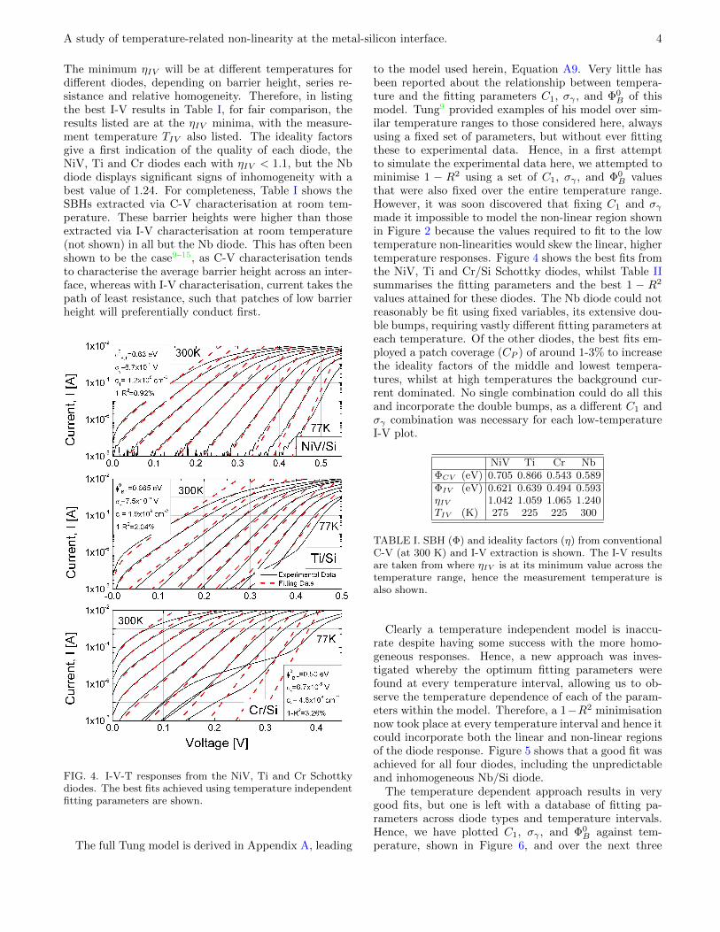
The minimum ηIV will be at different temperatures fordifferent diodes, depending on barrier height, series re-sistance and relative homogeneity. Therefore, in listingthe best I-V results in Table I, for fair comparison, theresults listed are at the ηIV minima, with the measure-ment temperature TIV also listed. The ideality factorsgive a first indication of the quality of each diode, theNiV, Ti and Cr diodes each with ηIV < 1.1, but the Nbdiode displays significant signs of inhomogeneity with abest value of 1.24. For completeness, Table I shows theSBHs extracted via C-V characterisation at room tem-perature. These barrier heights were higher than thoseextracted via I-V characterisation at room temperature(not shown) in all but the Nb diode. This has often beenshown to be the case9–15, as C-V characterisation tendsto characterise the average barrier height across an inter-face, whereas with I-V characterisation, current takes thepath of least resistance, such that patches of low barrierheight will preferentially conduct first.
FIG. 4. I-V-T responses from the NiV, Ti and Cr Schottkydiodes. The best fits achieved using temperature independentfitting parameters are shown.
The full Tung model is derived in Appendix A, leading
to the model used herein, Equation A9. Very little hasbeen reported about the relationship between tempera-ture and the fitting parameters C1, σγ , and Φ0
B of thismodel. Tung9 provided examples of his model over sim-ilar temperature ranges to those considered here, alwaysusing a fixed set of parameters, but without ever fittingthese to experimental data. Hence, in a first attemptto simulate the experimental data here, we attempted tominimise 1 − R2 using a set of C1, σγ , and Φ0
B valuesthat were also fixed over the entire temperature range.However, it was soon discovered that fixing C1 and σγmade it impossible to model the non-linear region shownin Figure 2 because the values required to fit to the lowtemperature non-linearities would skew the linear, highertemperature responses. Figure 4 shows the best fits fromthe NiV, Ti and Cr/Si Schottky diodes, whilst Table IIsummarises the fitting parameters and the best 1 − R2
values attained for these diodes. The Nb diode could notreasonably be fit using fixed variables, its extensive dou-ble bumps, requiring vastly different fitting parameters ateach temperature. Of the other diodes, the best fits em-ployed a patch coverage (CP ) of around 1-3% to increasethe ideality factors of the middle and lowest tempera-tures, whilst at high temperatures the background cur-rent dominated. No single combination could do all thisand incorporate the double bumps, as a different C1 andσγ combination was necessary for each low-temperatureI-V plot.
NiV Ti Cr NbΦCV (eV) 0.705 0.866 0.543 0.589ΦIV (eV) 0.621 0.639 0.494 0.593ηIV 1.042 1.059 1.065 1.240TIV (K) 275 225 225 300
TABLE I. SBH (Φ) and ideality factors (η) from conventionalC-V (at 300 K) and I-V extraction is shown. The I-V resultsare taken from where ηIV is at its minimum value across thetemperature range, hence the measurement temperature isalso shown.
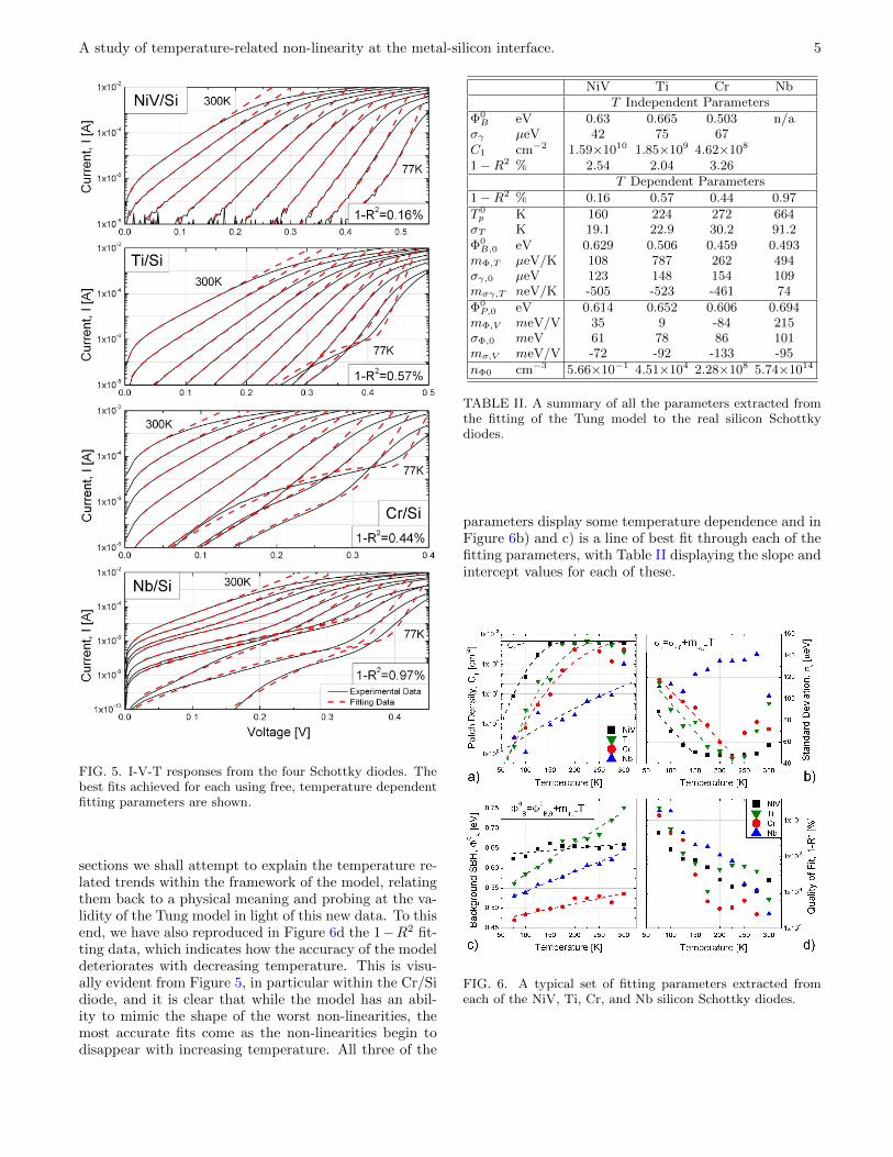
Clearly a temperature independent model is inaccu-rate despite having some success with the more homo-geneous responses. Hence, a new approach was inves-tigated whereby the optimum fitting parameters werefound at every temperature interval, allowing us to ob-serve the temperature dependence of each of the param-eters within the model. Therefore, a 1−R2 minimisationnow took place at every temperature interval and hence itcould incorporate both the linear and non-linear regionsof the diode response. Figure 5 shows that a good fit wasachieved for all four diodes, including the unpredictableand inhomogeneous Nb/Si diode.
The temperature dependent approach results in verygood fits, but one is left with a database of fitting pa-rameters across diode types and temperature intervals.Hence, we have plotted C1, σγ , and Φ0
B against tem-perature, shown in Figure 6, and over the next three
A study of temperature-related non-linearity at the metal-silicon interface. 5
FIG. 5. I-V-T responses from the four Schottky diodes. Thebest fits achieved for each using free, temperature dependentfitting parameters are shown.
sections we shall attempt to explain the temperature re-lated trends within the framework of the model, relatingthem back to a physical meaning and probing at the va-lidity of the Tung model in light of this new data. To thisend, we have also reproduced in Figure 6d the 1−R2 fit-ting data, which indicates how the accuracy of the modeldeteriorates with decreasing temperature. This is visu-ally evident from Figure 5, in particular within the Cr/Sidiode, and it is clear that while the model has an abil-ity to mimic the shape of the worst non-linearities, themost accurate fits come as the non-linearities begin todisappear with increasing temperature. All three of the
NiV Ti Cr NbT Independent Parameters
Φ0B eV 0.63 0.665 0.503 n/a
σγ µeV 42 75 67C1 cm−2 1.59×10¹⁰ 1.85×10⁹ 4.62×10⁸
1 −R2 % 2.54 2.04 3.26T Dependent Parameters
1 −R2 % 0.16 0.57 0.44 0.97T 0p K 160 224 272 664σT K 19.1 22.9 30.2 91.2Φ0B,0 eV 0.629 0.506 0.459 0.493
mΦ,T µeV/K 108 787 262 494σγ,0 µeV 123 148 154 109mσγ,T neV/K -505 -523 -461 74Φ0P,0 eV 0.614 0.652 0.606 0.694
mΦ,V meV/V 35 9 -84 215σΦ,0 meV 61 78 86 101mσ,V meV/V -72 -92 -133 -95nΦ0 cm−3 5.66×10⁻¹ 4.51×10⁴ 2.28×10⁸ 5.74×10¹⁴
TABLE II. A summary of all the parameters extracted fromthe fitting of the Tung model to the real silicon Schottkydiodes.
parameters display some temperature dependence and inFigure 6b) and c) is a line of best fit through each of thefitting parameters, with Table II displaying the slope andintercept values for each of these.
FIG. 6. A typical set of fitting parameters extracted fromeach of the NiV, Ti, Cr, and Nb silicon Schottky diodes.
A study of temperature-related non-linearity at the metal-silicon interface. 6
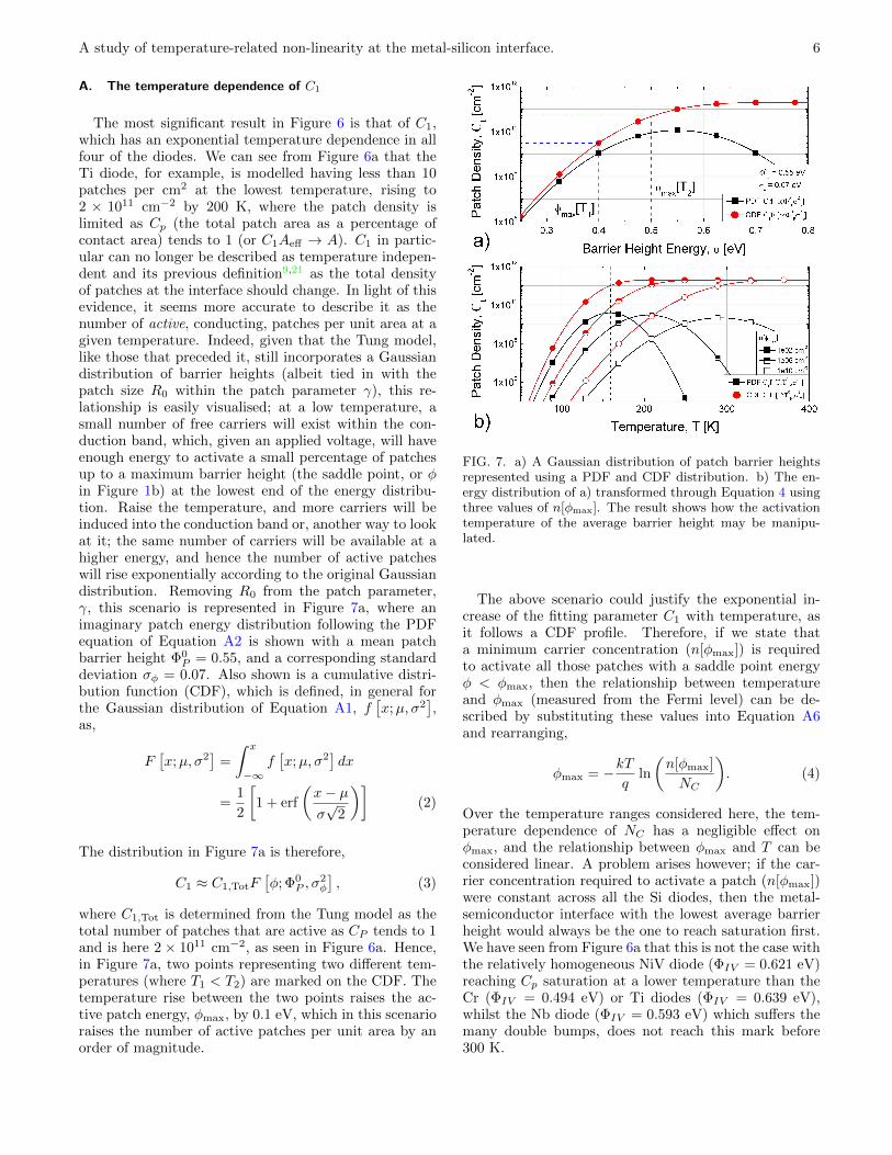
A. The temperature dependence of C1
The most significant result in Figure 6 is that of C1,which has an exponential temperature dependence in allfour of the diodes. We can see from Figure 6a that theTi diode, for example, is modelled having less than 10patches per cm2 at the lowest temperature, rising to2 × 1011 cm−2 by 200 K, where the patch density islimited as Cp (the total patch area as a percentage ofcontact area) tends to 1 (or C1Aeff → A). C1 in partic-ular can no longer be described as temperature indepen-dent and its previous definition9,21 as the total densityof patches at the interface should change. In light of thisevidence, it seems more accurate to describe it as thenumber of active, conducting, patches per unit area at agiven temperature. Indeed, given that the Tung model,like those that preceded it, still incorporates a Gaussiandistribution of barrier heights (albeit tied in with thepatch size R0 within the patch parameter γ), this re-lationship is easily visualised; at a low temperature, asmall number of free carriers will exist within the con-duction band, which, given an applied voltage, will haveenough energy to activate a small percentage of patchesup to a maximum barrier height (the saddle point, or φin Figure 1b) at the lowest end of the energy distribu-tion. Raise the temperature, and more carriers will beinduced into the conduction band or, another way to lookat it; the same number of carriers will be available at ahigher energy, and hence the number of active patcheswill rise exponentially according to the original Gaussiandistribution. Removing R0 from the patch parameter,γ, this scenario is represented in Figure 7a, where animaginary patch energy distribution following the PDFequation of Equation A2 is shown with a mean patchbarrier height Φ0
P = 0.55, and a corresponding standarddeviation σφ = 0.07. Also shown is a cumulative distri-bution function (CDF), which is defined, in general forthe Gaussian distribution of Equation A1, f
[x;µ, σ2
],
as,
F[x;µ, σ2
]=
∫ x
−∞f[x;µ, σ2
]dx
=1
2
[1 + erf
(x− µσ√
2
)](2)
The distribution in Figure 7a is therefore,
C1 ≈ C1,TotF[φ; Φ0
P , σ2φ
], (3)
where C1,Tot is determined from the Tung model as thetotal number of patches that are active as CP tends to 1and is here 2 × 1011 cm−2, as seen in Figure 6a. Hence,in Figure 7a, two points representing two different tem-peratures (where T1 < T2) are marked on the CDF. Thetemperature rise between the two points raises the ac-tive patch energy, φmax, by 0.1 eV, which in this scenarioraises the number of active patches per unit area by anorder of magnitude.
FIG. 7. a) A Gaussian distribution of patch barrier heightsrepresented using a PDF and CDF distribution. b) The en-ergy distribution of a) transformed through Equation 4 usingthree values of n[φmax]. The result shows how the activationtemperature of the average barrier height may be manipu-lated.
The above scenario could justify the exponential in-crease of the fitting parameter C1 with temperature, asit follows a CDF profile. Therefore, if we state thata minimum carrier concentration (n[φmax]) is requiredto activate all those patches with a saddle point energyφ < φmax, then the relationship between temperatureand φmax (measured from the Fermi level) can be de-scribed by substituting these values into Equation A6and rearranging,
φmax = −kTq
ln
(n[φmax]
NC
). (4)
Over the temperature ranges considered here, the tem-perature dependence of NC has a negligible effect onφmax, and the relationship between φmax and T can beconsidered linear. A problem arises however; if the car-rier concentration required to activate a patch (n[φmax])were constant across all the Si diodes, then the metal-semiconductor interface with the lowest average barrierheight would always be the one to reach saturation first.We have seen from Figure 6a that this is not the case withthe relatively homogeneous NiV diode (ΦIV = 0.621 eV)reaching Cp saturation at a lower temperature than theCr (ΦIV = 0.494 eV) or Ti diodes (ΦIV = 0.639 eV),whilst the Nb diode (ΦIV = 0.593 eV) which suffers themany double bumps, does not reach this mark before300 K.
A study of temperature-related non-linearity at the metal-silicon interface. 7
We therefore propose that n[φmax] is not the same forevery diode, and as such we here treat it as a variable thatis strongly influenced by the homogeneity of the contact,with a low value meaning that all the patches will be-come active at a low temperature, as in the NiV diode.This idea is demonstrated in Figure 7b, where the energy
distribution of Equation 3 and Figure 7a, F[φ; Φ0
P , σ2φ
],
has been transformed through Equation 4 using threedifferent values of n[φmax], to get,
C1 ≈ C1,TotF[T ;T 0
P , σ2T
]. (5)
Figure 7b shows clearly how the temperature responsewill spread, the corresponding values of T 0
P and σT beinggreatly affected by the size of n[φmax]. Given the low-est value of n[φmax] shown, 1 × 102 cm−3, the averagepatch of the distribution in Figure 7a will be activatedby 159 K, the large number of conducting patches at thistemperature meaning that the I-V response will be lin-ear. At the larger n[φmax] of 1× 1010 cm−3, nearly 3000times fewer patches will have been activated by 159 K,and the response at this temperature may well displaykinks. The average patch of this distribution would notbe activated until 300 K.
For the four diodes shown in Figure 6a, using another1 − R2 minimisation, it was possible to fit Equation 5to the temperature dependent parameters that were ex-tracted from the I-V-T modelling. Hence, for each diode,the best fit is shown in the Figure, with the values of T 0
p
and σT summarised in Table II. It can be seen that thevalues for the Nb diode far exceed that of the Cr andNiV diodes, which suggest that this diode may require alarge n[φmax] value to activate it patches.
B. The temperature dependence of σγ
As with the fitting parameter C1, the original Tungmodel9,11 offers no explicit mention of a σγ temperaturedependence, however Equation 24 of Tung’s model9 re-lates σγ to the ideality factor, expanded here as:
n ≈ 1 +σ2γV
2/3bb
3βη2/3. (6)
This relationship provides a direct link between the stan-dard deviation of the patch parameter and the idealityfactor profiles of Figure 3, explaining why, in general, thevalue of σγ seen in Figure 6b decreases with temperaturebefore rising again at higher temperatures as series resis-tance begins to skew the I-V profiles. This is particularlytrue of the Ti/Si diode, where the temperature responsesof nIV within Figure 3, and σγ in Figure 6b look verysimilar.
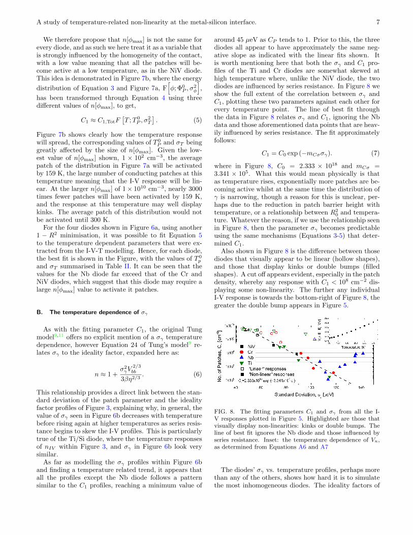
As far as modelling the σγ profiles within Figure 6band finding a temperature related trend, it appears thatall the profiles except the Nb diode follows a patternsimilar to the C1 profiles, reaching a minimum value of
around 45 µeV as CP tends to 1. Prior to this, the threediodes all appear to have approximately the same neg-ative slope as indicated with the linear fits shown. Itis worth mentioning here that both the σγ and C1 pro-files of the Ti and Cr diodes are somewhat skewed athigh temperature where, unlike the NiV diode, the twodiodes are influenced by series resistance. In Figure 8 weshow the full extent of the correlation between σγ andC1, plotting these two parameters against each other forevery temperature point. The line of best fit throughthe data in Figure 8 relates σγ and C1, ignoring the Nbdata and those aforementioned data points that are heav-ily influenced by series resistance. The fit approximatelyfollows:
C1 = C0 exp (−mCσσγ). (7)
where in Figure 8, C0 = 2.333 × 10¹⁸ and mCσ =3.341 × 10⁵. What this would mean physically is thatas temperature rises, exponentially more patches are be-coming active whilst at the same time the distribution ofγ is narrowing, though a reason for this is unclear, per-haps due to the reduction in patch barrier height withtemperature, or a relationship between R2
0 and tempera-ture. Whatever the reason, if we use the relationship seenin Figure 8, then the parameter σγ becomes predictableusing the same mechanisms (Equations 3-5) that deter-mined C1.
Also shown in Figure 8 is the difference between thosediodes that visually appear to be linear (hollow shapes),and those that display kinks or double bumps (filledshapes). A cut off appears evident, especially in the patchdensity, whereby any response with C1 < 108 cm−2 dis-playing some non-linearity. The further any individualI-V response is towards the bottom-right of Figure 8, thegreater the double bump appears in Figure 5.
FIG. 8. The fitting parameters C1 and σγ from all the I-V responses plotted in Figure 5. Highlighted are those thatvisually display non-linearities: kinks or double bumps. Theline of best fit ignores the Nb diode and those influenced byseries resistance. Inset: the temperature dependence of Vn,as determined from Equations A6 and A7
The diodes’ σγ vs. temperature profiles, perhaps morethan any of the others, shows how hard it is to simulatethe most inhomogeneous diodes. The ideality factors of
A study of temperature-related non-linearity at the metal-silicon interface. 8
the Nb/Si profile were taken from the linear regions of theprofile, above the double bumps, and hence the Nb ideal-ity factor profile in Figure 3 does not correlate with thevery large values of σγ in Figure 6b. For this Nb diode,there is little definitive correlation between C1 and σγ ,whilst in Figure 6b, we see a positive correlation betweenσγ and temperature and these large values of σγ , com-bined with the low values of C1 lead to the profile fullof double bumps up to 275 K seen in Figure 5. Giventhe evidence above linking σγ to both C1 and the experi-mental ideality factors, it is questionable whether a diodewith this degree of non-linearity may be modelled in thesame fashion.
C. The temperature dependence of Φ0B
Φ0B had previously been presumed to be stable across
the temperature range9,11. However, the fitting carriedout here could not have been completed with a fixed Φ0
B ,and Figure 6c displays the temperature dependence, andin general a positive, linear correlation over the temper-ature range is observed such that,
Φ0B = Φ0
B,0 +mφ,TT. (8)
This in itself is not surprising given the temperature de-pendence of Vn (Vn = EC − EF ), which is shown in theinset of Figure 8. Interfacial traps within the semicon-ductor bandgap causes the Fermi level of most semicon-ductors to be pinned at its surface25,28,29. This causesband bending to occur at the surface, prior to contactwith the metal, weakening the link between the Schot-tky barrier height and the work function offset, as laidout by the Schottky-Mott principle. This means that themagnitude of Vn directly influences the size of the barrierheight and its positive correlation with temperature, asseen in the inset of Figure 8, will cause an increase ofbarrier height with temperature.
D. The influence of carrier concentration n[φmax] on theTung model.
In the previous sections, we have shown how the threeparameters that make up the Tung model are themselvesrelated to temperature. In Figure 7, we showed how thetemperature dependent values of C1 can be extractedfrom an initial Gaussian distribution of maximum patch
barrier heights (C1,Totf[φ; Φ0
P , σ2φ
]) using Equation 4,
with the carrier concentration at a patch’s minimum bar-rier height, n[φmax], determining how homogeneous thatresponse will be. Having also defined the parameters σγand Φ0
B , we can now complete a full simulated example ofan I-V-T plot to show the influence that n[φmax] has on ageneric interface, making the difference between a homo-geneous response and one with extensive non-linearities.
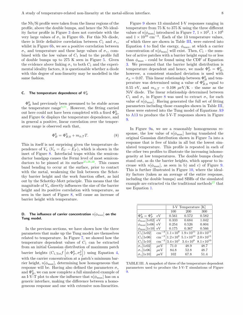
Figure 9 shows 13 simulated I-V responses ranging intemperature from 75 K to 375 K using the three differentvalues of n[φmax] introduced in Figure 7, 1× 10², 1× 10⁶
and 1 × 1010 cm−3. Each of the 13 temperature values,of which three are shown in Table III, were entered intoEquation 4 to find the energy, φmax, at which a carrierconcentration of n[φmax] will exist. Then, C1 - the num-ber of active patches with a barrier height equal to or lessthan φmax - could be found using the CDF of Equation3. We presumed that the barrier height distribution istemperature dependent and hence, we made Φ0
P = Φ0B ,
however, a consistent standard deviation is used withσφ = 0.07. This linear relationship between Φ0
B and tem-perature was determined using a value of Φ0
B,0 equal to
0.55 eV, and mφ,T = 0.108 µeV/K - the same as theNiV diode. The linear relationship determined betweenC1 and σγ in Figure 8 was used to extract σγ for eachvalue of n[φmax]. Having generated the full set of fittingparameters including those examples shown in Table III,these were entered into the Tung model of Equations A9to A13 to produce the I-V-T responses shown in Figure9.
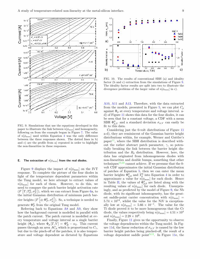
In Figure 9a, we see a reasonably homogeneous re-sponse, the low value of n[φmax] having translated theoriginal Gaussian distribution shown in Figure 7a into aresponse that is free of kinks in all but the lowest sim-ulated temperature. This profile is repeated in each ofthe other two profiles to illustrate the increasing inhomo-geneity at low temperatures. The double bumps clearlystand out, as do the barrier heights, which appear to in-crease with n[φmax], as seen in b) and c) of Figure 9.This is further illustrated in Figure 10, where the ideal-ity factors (taken as an average of the entire response,including the double bumps) and SBHs of the simulatedexample are extracted via the traditional methods27 thatuse Equation 1.
I-V Temperature [K]100 200 300
Φ0B = Φ0
P eV 0.561 0.572 0.582φmax[1e02] eV 0.333 0.684 1.042φmax[1e06] eV 0.254 0.526 0.804φmax[1e10] eV 0.175 0.367 0.566C1[1e02] cm−2 1.1×10⁸ 1.9×10¹¹ 2.0×10¹¹
C1[1e06] cm−2 1.2×10⁶ 5.1×10¹⁰ 2.0×10¹¹
C1[1e10] cm−2 3.4×10³ 3.4×10⁸ 8.1×10¹⁰
σγ [1e02] µeV 71.0 48.9 48.7σγ [1e06] µeV 84.8 52.8 48.7σγ [1e10] µeV 102 67.8 51.4
TABLE III. A snapshot of three of the temperature dependentparameters used to produce the I-V-T simulations of Figure9.
A study of temperature-related non-linearity at the metal-silicon interface. 9
FIG. 9. Simulations that use the equations developed in thispaper to illustrate the link between n[φmax] and homogeneity,following on from the example begun in Figure 7. The valueof n[φmax] used within Equation 4 was the only differencebetween the three responses shown. The dotted lines in b)and c) are the profile from a) repeated in order to highlightthe non-linearities in these responses.
E. The extraction of n[φmax] from the real diodes.
Figure 9 displays the impact of n[φmax] on the IVTresponse. To complete the picture of the four diodes inlight of the temperature dependent parameters withinthe Tung model, we here attempt to extract values ofn[φmax] for each of them. However, to do this, weneed to compare the patch barrier height activation rate(F[T ;T 0
P , σ2T
]), which we can extract from Figure 6a, to
the initial Gaussian distribution of minimum patch bar-
rier heights (F[φ; Φ0
P , σ2φ
]). So, a technique is needed to
generate Φ0P from the original Tung model.
Referring back to Equations A8 and A9, they showhow the background current is modelled in parallel withthe patch current. The patch current is modelled at ev-ery temperature and voltage interval as a single barrierheight (Φp), where Φp [T, V ] = Φ0
B − α2. This currentpasses through an area ACp which is proportional to C1,but due to the pinch-off of the patches, it is also temper-ature and voltage dependent as dictated by Equations
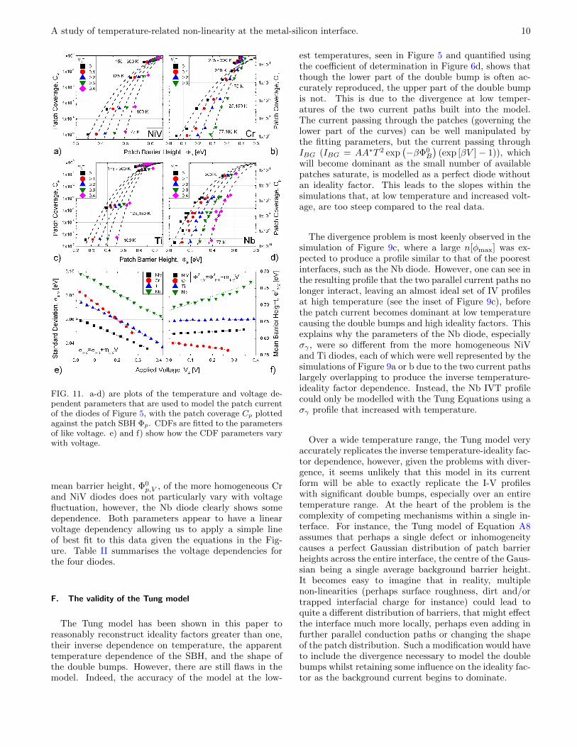
FIG. 10. The results of conventional SBH (a) and idealityfactor (b and c) extraction from the simulations of Figure 9.The ideality factor results are split into two to illustrate thedivergence problems of the larger value of n[φmax] in c).
A10, A11 and A13. Therefore, with the data extractedfrom the models, presented in Figure 5, we can plot Cpagainst Φp at every temperature and voltage interval. a-d) of Figure 11 shows this data for the four diodes, it canbe seen that for a constant voltage, a CDF with a meanSBH Φ0
p,V and a standard deviation σφ,V can easily befit to this data.
Considering just the 0-volt distributions of Figure 11a-d), they are reminiscent of the Gaussian barrier heightdistributions within, for example, Werner and Guttler’spaper13, where the SBH distribution is described with-out the rather abstract patch parameter, γ, so poten-tially breaking the link between the barrier height dis-tribution and the R0 distribution. However, here, thedata has originated from inhomogeneous diodes withnon-linearities and double bumps, something that othertechniques13,22 cannot achieve. If we presume that the 0-volt CDF approximates the initial Gaussian distributionof patches of Equation 5, then we can enter the meanbarrier heights Φ0
p,0 and T 0p into Equation 4 in order to
approximate a value for n[φmax] for each diode. Hencein Table II, the values of Φ0
p,0 are listed along with theresulting values of n[φmax] for each diode. Unsurpris-ingly, and as predicted by the model of Figure 9, the Nbdiode, with its significant inhomogeneity, has the great-est saddle-point carrier concentration with n[φmax] =5.74 × 10¹⁴, whilst the value for the NiV is exception-ally low at n[φmax] = 5.66 × 10⁻¹. The value for theTi diode proved it to be more homogeneous that the Crdiode, the values respectively being n[φmax] = 4.51× 10⁴
and n[φmax] = 2.28× 10⁸.Finally, Figure 11 gives us the opportunity to observe
the voltage dependencies within the Tung model. In Fig-ure 11d, the linear reduction of σφ,V is caused by the lowbarrier height patches being pinched-off, the result of avoltage dependent saddle point9,11. In Figure 11e, the
A study of temperature-related non-linearity at the metal-silicon interface. 10
FIG. 11. a-d) are plots of the temperature and voltage de-pendent parameters that are used to model the patch currentof the diodes of Figure 5, with the patch coverage Cp plottedagainst the patch SBH Φp. CDFs are fitted to the parametersof like voltage. e) and f) show how the CDF parameters varywith voltage.
mean barrier height, Φ0p,V , of the more homogeneous Cr
and NiV diodes does not particularly vary with voltagefluctuation, however, the Nb diode clearly shows somedependence. Both parameters appear to have a linearvoltage dependency allowing us to apply a simple lineof best fit to this data given the equations in the Fig-ure. Table II summarises the voltage dependencies forthe four diodes.
F. The validity of the Tung model
The Tung model has been shown in this paper toreasonably reconstruct ideality factors greater than one,their inverse dependence on temperature, the apparenttemperature dependence of the SBH, and the shape ofthe double bumps. However, there are still flaws in themodel. Indeed, the accuracy of the model at the low-
est temperatures, seen in Figure 5 and quantified usingthe coefficient of determination in Figure 6d, shows thatthough the lower part of the double bump is often ac-curately reproduced, the upper part of the double bumpis not. This is due to the divergence at low temper-atures of the two current paths built into the model.The current passing through the patches (governing thelower part of the curves) can be well manipulated bythe fitting parameters, but the current passing throughIBG (IBG = AA∗T 2 exp
(−βΦ0
B
)(exp [βV ]− 1)), which
will become dominant as the small number of availablepatches saturate, is modelled as a perfect diode withoutan ideality factor. This leads to the slopes within thesimulations that, at low temperature and increased volt-age, are too steep compared to the real data.
The divergence problem is most keenly observed in thesimulation of Figure 9c, where a large n[φmax] was ex-pected to produce a profile similar to that of the poorestinterfaces, such as the Nb diode. However, one can see inthe resulting profile that the two parallel current paths nolonger interact, leaving an almost ideal set of IV profilesat high temperature (see the inset of Figure 9c), beforethe patch current becomes dominant at low temperaturecausing the double bumps and high ideality factors. Thisexplains why the parameters of the Nb diode, especiallyσγ , were so different from the more homogeneous NiVand Ti diodes, each of which were well represented by thesimulations of Figure 9a or b due to the two current pathslargely overlapping to produce the inverse temperature-ideality factor dependence. Instead, the Nb IVT profilecould only be modelled with the Tung Equations using aσγ profile that increased with temperature.
Over a wide temperature range, the Tung model veryaccurately replicates the inverse temperature-ideality fac-tor dependence, however, given the problems with diver-gence, it seems unlikely that this model in its currentform will be able to exactly replicate the I-V profileswith significant double bumps, especially over an entiretemperature range. At the heart of the problem is thecomplexity of competing mechanisms within a single in-terface. For instance, the Tung model of Equation A8assumes that perhaps a single defect or inhomogeneitycauses a perfect Gaussian distribution of patch barrierheights across the entire interface, the centre of the Gaus-sian being a single average background barrier height.It becomes easy to imagine that in reality, multiplenon-linearities (perhaps surface roughness, dirt and/ortrapped interfacial charge for instance) could lead toquite a different distribution of barriers, that might effectthe interface much more locally, perhaps even adding infurther parallel conduction paths or changing the shapeof the patch distribution. Such a modification would haveto include the divergence necessary to model the doublebumps whilst retaining some influence on the ideality fac-tor as the background current begins to dominate.
A study of temperature-related non-linearity at the metal-silicon interface. 11
IV. CONCLUSIONS
A study of the temperature dependencies inherentwithin the Tung model was presented. The aim of thework was to produce a model that could better repro-duce the non-linearities present in log(I)− V plots, overa wide temperature range, hence improving our abilityto predict the behaviour of real metal-silicon interfaces.In doing so we have presented both the strengths andweaknesses of the original model and made suggestionsas to how the previously unexplored temperature depen-dencies within the model may be interpreted.
In particular, four silicon Schottky diodes were mod-elled, a comparatively homogeneous NiV diode, a Ti anda Cr diode displaying low temperature inhomogeneity,and a Nb diode displaying double bumps right up toroom temperature. A semi-automated implementationof Tung’s electron transport model was shown to gen-erate accurate fits, though we documented some diver-gence problems at low temperature, and with extremelyinhomogeneous interfaces. To achieve the fits, the threefitting parameters had to be individually optimised atevery temperature interval, revealing a significant tem-perature dependence in each of them. This included theparameter C1, which was thought to represent the totalnumber of patches at an interface irrespective of temper-ature. However, C1 was shown to increase exponentiallywith temperature, such that it fit a normal cumulativedensity function (CDF) with a mean temperature, anda corresponding standard deviation. We therefore sug-gest that C1 is better defined as the number of activepatches at a given temperature, whose saddle point isequal to or less than the energy that a conduction bandelectron may attain. In investigating this further, a linkto interfacial homogeneity was found; we showed that theparameter nφ, the carrier concentration at the minimumsaddle energy, could control the degree of non-linearity(high ideality factors and double bumps) present withina full I-V-T profile. Furthermore, for each of the diodestested in this paper, a value of nφ was estimated usinga Gaussian SBH distribution extracted from the originalmodel. The comparatively homogeneous NiV diode wasshown to have a carrier concentration at φmax many or-ders of magnitude less than that of the inhomogeneousNb diode. Finally, in a review of the model, the prob-lems of divergence at low temperature were explained tobe inherent due to the simplification of an interface thatwill contain competing defects and inhomogeneities.
Peter Gammon would like to gratefully acknowledgethe financial support from the Royal Academy of En-gineering. This work was supported by EPSRC grantEP/G060940/1, Nanostructured Functional Materials forEnergy Harvesting.
Appendix A: The Tung Model
According to Tung’s model of “Electron transport atmetal-semiconductor interfaces”9, two components con-tribute to the current across a metal-semiconductor inter-face. That from the background current, IBG, is mod-elled as a homogeneous interface, as a current passingover a uniform barrier height, Φ0
B , via thermionic emis-sion (Equation 1). This occurs in parallel with a secondcurrent that passes over the many inhomogeneous, volt-age dependent patches of varying barrier height. Theindividual patches are presumed circular with a radius,R0, each with a potential “depth”, ∆, from Φ0
B21. Tung9
defined a patch parameter, γ, that encompassed both ofthese parameters such that γ = 3(∆R2
0/4)1/3. γ can bedescribed by a probability density function (PDF), P [x],which, in general is described by
P [x] =
∫ ∞−∞
f [x;µ, σ2] (A1)
=1
σ√
2π
∫ ∞−∞
exp
(− (x− µ)
2
2σ2
)dx, (A2)
where σ is the standard deviation, and µ the mean of thevariable x. Specifically for the patch parameter, a PDFis defined, P [γ], and hence, given a mean value of 0, thedistribution is defined as,
f [γ;σ2γ ] =
1
σγ√
2πexp
(− γ2
2σ2γ
). (A3)
The current passing through a single patch wasdefined9 taking into account the pinch-off effect on thelow SBHs, and the voltage dependency of the saddlepoint:
Ipatch[γ, V ] = AeffA∗T 2 exp
(−β
[Φ0B −
γV1/3bb
ζ1/3
])× (exp [βV ]− 1) (A4)
where, ζ = εs/qnno, Vbb = Φ0B−Vn−V , εs is the permit-
tivity of the semiconductor and Vn the energy differencebetween the Fermi level and the conduction band. Aeff
is the localised effective area of a single patch, a temper-ature dependent variable defined9,10,21 as,
Aeff =4πγζ2/3
9βV2/3bb
(A5)
At 300 K, the number of free carriers within the con-duction band, nno, may all be presumed to be from thephosphorous dopants (ND = 1 × 1016 cm−3), with theintrinsic carrier concentration (ni) being negligible (lessthan 1× 1010 cm−3). However, dopant freeze out at thelower temperatures does have to be considered. Hence,
A study of temperature-related non-linearity at the metal-silicon interface. 12
from Sze26, nno was found by solving graphically for theFermi level energy (EF ) given that,
nno = NC exp
(−EC − EF
kT
)(A6)
≈ ND1 + 2 exp [(EF − ED) /kT ]
(A7)
where ND is the density of the dopants, NC is the den-sity of states in the conduction band, EC is the lowerconduction band edge and ED the phosphorous donorenergy, which lies 0.046 eV below EC
26. Along with nno,NC was also considered temperature dependent, as wasEF and Vn, with temperature related equations for eachfound in26.
The total current passing through the interface is foundby combining Equations 1, A3, A4 and A5,
I = C1A
∫ ∞−∞
f [γ;σ2γ ]Ipatch [γ, V ] dγ + IBG [V ] (A8)
= AA∗T 2 exp(−βΦ0
B
)(exp [βV ]− 1)
×{1− Cp + Cp exp (βα2)} (A9)
where C1 is the areal density of patches with units ofcm−2 and Cp is the percentage area taken up by lowbarrier patches, with
Cp ≈ C1Aeff
= α1α3. (A10)
The values α1, α2 and α3 are temperature and voltagedependent variables given by,
α1 =2πC1σ
2γζ
1/3
9V1/3bb
, (A11)
α2 =βσ2
γV2/3bb
2ζ2/3, (A12)
α3 = 1 + erf(√
βα2
), (A13)
Although rewritten here, this is the same model adaptedfrom Tung’s original work9 by Im et al21, to reduce thecontribution of the background current by the percent-age area (Cp) taken up by low barrier patches. WithinEquation A9, three fitting parameters need to be selectedto model any given I-V response; C1, σγ , and Φ0
B . Therest of Equations A9-A13 can be derived from fundamen-tal constants, or from materials properties, which are of-ten individually temperature or voltage dependent. Thesize of C1 had to be limited (typically to a maximum of1 × 1012 cm−2) to prevent the fractional coverage, CPexceeding 1.
Appendix B: The coefficient of determination.
The coefficient of determination is defined as,
R2 = 1−
∑i
(yi − y)2
∑i
(yi − fi)2(B1)
where for every point on the x-axis (the voltage-axis), yiis the experimental data point and fi the correspondingdata point from the model. y is the average of all theexperimental data points. Herein,
yi = log (IV,Exp) , (B2)
fi = log (IV,Fit) , (B3)
y =1
n
n∑i
log (IV,Exp) . (B4)
As a good fit could be R2 = 99.99%, throughout this pa-per the quality of fit is presented as a percentage, definedby 1−R2, and hence 0% would be a perfect fit.
1B. Ozpineci and L. Tolbert, “Smaller, faster, tougher”, IEEESpectrum, 48, 10 45 (2011).
2A. Fontsere , A. Perez-Tomas, M. Placidi, J. Llobet, N. Baron,S. Chenot, Y. Cordier, J. C. Moreno, M. R. Jennings, P. M. Gam-mon, C. A. Fisher, V. Iglesias, M. Porti, A. Bayerl, M. Lanza andM. Nafra, Nanotechnology 23 395204 (2012).
3M. Asif Khan, A. Bhattarai, J. N. Kuznia, and D. T. Olson,Appl. Phys. Lett. 63, 1214 (1993).
4N. Miura, T. Nanjo, M. Suita, T. Oishi, Y. Abe, T. Ozeki,H. Ishikawa, T. Egawa and T. Jimbo, Solid-State Elec., 48, 5689, (2004).
5P. M. Smith, IEEE Transactions on Microwave Theory andTechniques 44, 12 2328 (1996).
6S. Heinze, J. Tersoff, R. Martel, V. Derycke, J. Appenzeller, andPh. Avouris, Phys. Rev. Lett. 89, 106801 (2002).
7J. M. Luther, M. Law, M. C. Beard, Q. Song, M. O. Reese,R. J. Ellingson, and A. J. Nozik, Nano Lett. 10 8 3488 (2008).
8X. Li, H. Zhu, K. Wang, A. Cao, J. Wei, C. Li, Y. Jia, Z. Li,X. Li and D. Wu, Adv. Mater., 22 2743 (2010).
9R. T. Tung, Phys. Rev. B, 45, 13509 (1992).10J. P. Sullivan, R. T. Tung, M. R. Pinto, and W. R. Graham, J.Appl. Phys., 70, 7403 (1991)
11R. T. Tung, Mat. Sci. Eng., 35, 1 (2001).12P. M. Gammon, A. Perez-Tomas, V. A. Shah, G. J. Roberts,
M. R. Jennings, J. A. Covington, and P. A. Mawby J. Appl.Phys. 106, 093708 (2009).
13J. H. Werner and H. H. Guttler, J. Appl. Phys. 69, 1522 (1991).14J. L. Freeouf, T. N. Jackson, S. E. Laux, and J. M. Woodall, J.Vac. Sci. Technol., 21, 2570 (1982).
15I. Ohdomari and K. N. Tu, J. Appl. Phys. 51, 3735 (1980).16D. Defives, O. Noblanc, C. Dua, C. Brylinski, M. Barthula and
F. Meyer, Mat. Sci. and Eng: B, 61, 395 (1999).17B. J. Skromme, E. Luckowski, K. Moore, M. Bhatnagar,
C. E. Weitzel, T. Gehoski and D. Ganser, J. Elec. Mat. 29, 376(2000).
18I. Nikitina, K. Vassilevski, A. Horsfall, N. Wright, A. G. O’Neill,S. K. Ray, K. Zekentes and C. M. Johnson, Semicond. Sci. Tech-nol. 24, 055006 (2009).
19D. J. Ewing, L. M. Porter, Q. Wahab, X. Ma, T. S. Sudharshan,S. Tumakha, M. Gao, and L. J. Brillson J. Appl. Phys. 101,114514 (2007).
A study of temperature-related non-linearity at the metal-silicon interface. 13
20X. Ma,P. Sadagopan and T. S. Sudarshan Phys. Stat. Sol. a 203,643 (2006).
21H. J. Im, Y. Ding, J. P. Pelz and W. J. Choyke, Phys. Rev. B,64, 075310, (2001).
22F. Roccaforte, F. La Via, V. Raineri, R. Pierobon, and E. Zanoni,J. Appl. Phys., 93, 9137 (2003).
23D. Korucu, H. Efeoglu, A. Turut,, and S. Altindal, Mat. Sci.Semicond. Proc., 15, 5 480 (2012)
24A. Bengi, S. Altindal, S. Ozcelik and T. S. Mammadov, PhysicaB, 396, 22 (2007).
25P. M. Gammon, A. Perez-Tomas, M. R. Jennings, V. A. Shah,S. A. Boden, M. C. Davis, S. E. Burrows, N. R. Wilson,
G. J. Roberts, J. A. Covington, and P. A. Mawby J. Appl. Phys.,107, 124512 (2010).
26S. M. Sze and K. K. Ng, Physics of Semiconductor Devices, (Wi-ley, New York, 2007). Si Dopant and freeze out calculations: pp23-26.
27D. K. Schroder, Semiconductor Material and Device Character-ization, p. 158 (Wiley, New York, 1998).
28W. Monch, Electronic Properties of Semiconductor Interfaces,(Springer, Berlin, 2004).
29R. T. Tung, Mat. Sci. Eng., 35, 1 (2001).