Embed Size (px)
Citation preview

Li, Jianfeng and Mouawad, Bassem and Castellazzi, Alberto and Friedrichs, Peter and Johnson, Christopher Mark (2016) Low parasitic inductance multi-chip SiC devices packaging technology. In: 18th European Conference on Power Electronics and Applications, 5-9 September 2016, Karlsruhe, Germany.
Access from the University of Nottingham repository: http://eprints.nottingham.ac.uk/37316/1/Low%20parasitic%20inductance%20multi-chip%20SiC%20devices%20packaging%20technology.pdf
Copyright and reuse:
The Nottingham ePrints service makes this work by researchers of the University of Nottingham available open access under the following conditions.
This article is made available under the University of Nottingham End User licence and may be reused according to the conditions of the licence. For more details see: http://eprints.nottingham.ac.uk/end_user_agreement.pdf
A note on versions:
The version presented here may differ from the published version or from the version of record. If you wish to cite this item you are advised to consult the publisher’s version. Please see the repository url above for details on accessing the published version and note that access may require a subscription.
For more information, please contact [email protected]

Low parasitic inductance multi-chip SiC devices packaging technology
Bassem Mouawad1, Jianfeng Li1, Alberto Castellazzi1, Peter Friedrichs2, C. Mark Johnson1 1 Power Electronics, Machines and Control Group (PEMC), University of Nottingham,
University Park Campus, NG7 2RD, Nottingham, United Kingdom
Tel: +44-(0)115-846-6890
2 Infineon AG, Schottkystrasse 10, 91058 Erlangen, Germany
E-mail: [email protected]
URL: http://www.nottingham.ac.uk/
Acknowledgements
This work is supported by the SPEED (Silicon Carbide Power Technology for Energy
Efficient Devices) Project funded by the European commission FP7-Grant #:604057.
Keywords
« Wide bandgap devices », « High frequency power converter» , « Silicon Carbide (SiC) »,
« Packaging », « high voltage power converters », « JFET » « Wind energy »
Abstract
This paper presents a novel packaging structure which employs stacked substrate and flexible
printed circuit board (PCB) to obtain very low parasitic inductance and hence feature high
switching speed SiC power devices. A half-bridge module aimed at blocking voltage up to
2.5kV has been designed to accommodate 8 SiC JFETs and 4 SiC diodes. Electromagnetic
simulation results reveal extremely low inductance values of the major loops. Then the
prototyping of the designed package including the assembly process, all the electrical test to
evaluate the electrical performance are presented.
Introduction
Power semiconductor devices have largely improved since they were first introduced more
than 50 years ago. The recent availability of silicon carbide (SiC) devices has pushed the
boundaries even further in terms of power density, conversion efficiency, switching speed or
thermal capability. In fact, they are enabling components mainly if higher switching
frequencies in power electronics are considered. However, this trend imposes new challenges
towards the package of these devices where stray parasitic inductances become crucial
concern specially to avoid the high spikes due to high 𝑑𝑖 𝑑𝑡⁄ and 𝑑𝑉 𝑑𝑡⁄ under high switching
frequency. Hence, new packaging solution is needed to reduce the stray parasitic inductance
for addressing this concern.
On the other hand, the most common technology of a die-level interconnect is wire bonding.
Maturity, flexibility and low cost are main factors, which explain the use of the wire bonding
technology. However, it has electrical limitation (such as parasitic inductance) and thermo-
mechanical limitations such as thermal stress leading to the fatigue and eventually a failure.
Alternative interconnection technologies have been developed to overcome these
shortcomings, allowing a three-dimensional (3D) packaging of power modules in a compact
stacked layer structure [1]–[7]. The technology used in the reported works mainly uses a
conventional layout of DBC substrates on both sides of the devices to allow a double-side
cooling. It should also be noted that the majority of the work reported was applied to low-
voltage devices and applications.
In this paper, a new design of a power module is presented, with very low parasitic inductance
specifications. The presented design is targeting the relatively high voltage SiC devices and
it’s based on an optimization of the conductors’ geometry, having the input and output
conductors to be parallel with narrow separation, and hence, cancelling by that the
electromagnetic field that determines the inductance. The concept was recently reported [8].
In this paper, the assembling process is presented in details and the assembled prototype is
tested electrically using both static and dynamic tests.
Design of the low parasitic inductance half bridge
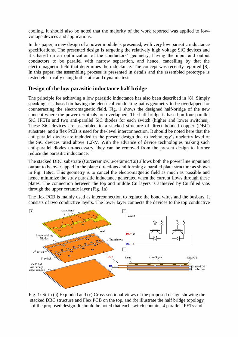
The principle for achieving a low parasitic inductance has also been described in [8]. Simply
speaking, it’s based on having the electrical conducting paths geometry to be overlapped for
counteracting the electromagnetic field. Fig. 1 shows the designed half-bridge of the new
concept where the power terminals are overlapped. The half-bridge is based on four parallel
SiC JFETs and two anti-parallel SiC diodes for each switch (higher and lower switches).
These SiC devices are assembled to a stacked structure of direct bonded copper (DBC)
substrate, and a flex PCB is used for die-level interconnection. It should be noted here that the
anti-parallel diodes are included in the present design due to technology’s unclarity level of
the SiC devices rated above 1.2kV. With the advance of device technologies making such
anti-parallel diodes un-necessary, they can be removed from the present design to further
reduce the parasitic inductance.
The stacked DBC substrate (Cu/ceramic/Cu/ceramic/Cu) allows both the power line input and
output to be overlapped in the plane directions and forming a parallel plate structure as shown
in Fig. 1a&c. This geometry is to cancel the electromagnetic field as much as possible and
hence minimize the stray parasitic inductance generated when the current flows through these
plates. The connection between the top and middle Cu layers is achieved by Cu filled vias
through the upper ceramic layer (Fig. 1a).
The flex PCB is mainly used as interconnection to replace the bond wires and the busbars. It
consists of two conductive layers. The lower layer connects the devices to the top conductive
Fig. 1: Strip (a) Exploded and (c) Cross-sectional views of the proposed design showing the
stacked DBC structure and Flex PCB on the top, and (b) illustrate the half bridge topology
of the proposed design. It should be noted that each switch contains 4 parallel JFETs and
two anti-parallel diodes.

layer of the flex. The latter contains:
The connection to AC track designed in a way to be overlapped in the plane directions
with DC+ track.
The connection of the source pads of 1st switch to drain pads of the 2nd switch.
The connection of source of the 2nd leg to DC- track on the DBC.
The connections for the gate signals to control the JFETs.
It should be noted that the designed package could be compatible with a voltage rate up to
2.5kV for any design margin the device manufacturer takes on the nominal breakdown
voltage by tailoring the thickness of insulating materials.
Electromagnetic simulation of the new package design
The commercial electromagnetic simulation software, MAXWELL 3D, was used to calculate
the parasitic parameters associated with the new package design. Fig. 2a shows a cross-
sectional drawing illustrating the two major electrical current loops used for the
electromagnetic simulation, where loop 1 illustrates the current flowing from DC+ to DC-
through the JFETs of the 1st switch and the Diodes of the 2nd switch, and Loop 2 illustrates the
current flowing from DC- to DC+ through the JFETs of the 2nd switch and the Diodes of the
1st switch. As the thickness of the ceramic in DBC substrates could be different depending on
the applications and the electrical insulation abilities of a power module, two thicknesses, i.e.
300µm and 635µm, were considered. Fig. 2b shows the extracted parasitic inductance as a
function of frequency for the two loops with the two thicknesses of the ceramic. The parasitic
inductance of the major loops is ranging from 1.7 to 2.2nH and from 2.1 to 2.6nH at 1kHz for
300µm and 635µm thick ceramic, respectively. The inductance of the inner loop becomes
extremely low since DC+ and DC- tracks are routed on top of each other as shown in Fig. 1c.
These value are comparable to the extracted inductance value reported in [9] where they are
using FR4 PCB to achieve a similar geometry configuration.
Fig. 2: (a) Illustration of the two electrical current loops used for the electromagnetic
simulation used & (b) the quantified inductance of the two loops for two spacing value
between the input and output terminal which correspond to the thickness of ceramic layer in
the stacked DBC substrate.

Components and assembling technology
Parts
Fig. 3 shows the parts used to build the designed package. These are described as follows:
4x 1.2kV/2.7mmx2.7mm SiC Diodes with Cu-based finishing metal layer; 2 Diodes per
switch
8x 1.2kV/3.2mmx3.2mm SiC JFETs with Cu-based finishing metal layer; 4 JFETs per
switch
635µm thick AlN-based stacked DBC substrate
Flex PCB
Pins for Gate terminal connections
Ag pins for connecting the Flex PCB to the stacked DBC substrates
Assembly process
Fig. 4 illustrates the presently assembling process flow. Prior to the assembling process, both
the Flex PCB and Cu-based SiC JFETs and SiC Diodes are chemically cleaned using acetone
and isopropanol solutions. Plasma etching was then used to remove any residual organic
contamination and for deoxidization of SiC devices.
First, solder paste was stencil-printed on the copper track of the Flex PCB. Because the
3.2mmx3.2mm SiC JFETs have relatively fine patterns, an accurate die bonder had been
employed for accurate die placing to avoid potential short-circuiting between the gate and
source. The Flex PCB with the SiC devices was then heated to melt the solder paste and to
form the connection between the Cu tracks of the Flex PCB to the Cu track on the topside of
the SiC devices. Fig. 4d shows the SiC devices and the Ag pins bonded on the top of the Flex
PCB.
Once all the components are soldered to the Flex PCB, the backsides of them will be further
bonded to the stacked DBC substrate. Fig. 4e shows the part after that stage with the Gate
Fig. 3: Parts used for the designed package

Terminals pins soldered on the topside of the Flex PCB. Finally, insulating silicone gel was
injected into the gap between the stacked DBC substrate and the Flex PCB.
Electrical test
Static test
A static current-voltage characteristics test was carried out to test the forward characteristics
of the JFETs at room temperature. Fig. 5 illustrates the result for 4 parallel SiC JFETs with
different gate voltage. It can be seen the currents at different gate voltages are all comparable
with the values of 4 times of the values for single SiC JFET [10]. Therefore it can be
concluded that all the 4 SiC JFETs have been effectively controlled by the gate signal which
Fig. 4: Illustration of the process flow for assembling the designed package
Fig. 5: Forward characteristics of 4 parallel SiC
JFETs with different gate voltage

means the designed connection has been achieved.
Dynamic test
Double-pulse test is a widely used approach to characterize the parasitic electric parameters of
power module packaging and to test the switching performance of the latter. It is performed
by operating the phase leg (or half bridge) module in a standard switching process including
switch-on, conduction, switch-off and block with inductive load, which can control the
current going through the switches and voltage applied. This test was carried out at room
temperature on the designed package.
The experimental parameters are list below in Table I. The lower sides 4 parallel SiC JFETs
of the half bridge are the devices under test (DUT) and the inductor is connected in parallel
with the higher side switch. The driving signal is switched between 0V and -18V. The load
Table I: Experimental parameters for Double Pulse test
Part Type
Drain-Source current (IDS) 17A
Bus voltage (Vbus) 400V
Gate voltage (VGS) 0V/-18V
Gate resistance (Rg) 10Ω
Load inductance (Lload) 420µH
Junction temperature (Tj) 25°C (Room temperature)
Oscilloscope Tektronix DPO 7104
(BW=500MHz)
Voltage probe Differential probe
(BW=50MHz)
Current sensor Rogowski coil PEM CWT1
(BW=20MHz)
Fig. 6: Double-pulse test at room temperature showing the switching waveforms of 4 parallel
SiC JFETs for the turn-off and turn on state (Vgate=0V/-18V; Rg=10Ω)

current is 17A. The DC-Link Voltage is 400V. Fig. 6 presents the voltage and current
waveforms of the lower 4x SiC JFETs during the switching off and on transient in the
designed package. It can be seen that the voltage overshoot during the turn-off transient is
quite low which means the parasitic inductance is low as intended by the design. However,
the current overshoot during the turn-on transient is quite high. This is believed to be due to
the gate driver as revealed by the gate voltage waveform. It should be mentioned that the gate
driver used for this test is an existing gate driver in our lab but not designed specifically for
this module.
Conclusion
With SiC power devices reaching nearly perfect switching properties the parasitic effects
around them start to determine the performance. This paper outlined a novel packaging design
that reduces drastically these parasitic effects by optimizing the geometry of conductors. An
electromagnetic simulation shows a very low parasitic inductance of the DC-link loop. The
complete manufacturing process, which offer a high accuracy level to the fine layout of the
SiC devices has been described in details. Electrical tests, both static current-voltage
characteristics and dynamic transient show a good electrical performance of the 4 parallel SiC
JFETs.
References
[1] P. Beckedahl, M. Spang, and O. Tamm, “Breakthrough into the third dimension – Sintered multi layer flex
for ultra low inductance power modules,” in 8th International Conference on Integrated Power Electronics
Systems (CIPS), 2014, pp. 461–465.
[2] J. N. Calata, J. G. Bai, X. Liu, S. Wen, and G.-Q. Lu, “Three-Dimensional Packaging for Power
Semiconductor Devices and Modules,” IEEE Trans. Adv. Packag., vol. 28, no. 3, pp. 404–412, 2005.
[3] X. He, X. Zeng, X. Yang, and Z. Wang, “A Hybrid Integrated Power Electronic Module Based On Pressure
Contact Technology,” in 37th IEEE Power Electronics Specialists Conference, 2006.
[4] E. Vagnon, J. C. Crebier, Y. Avenas, and P. O. Jeannin, “Study and realization of a low force 3D press-
pack power module,” in Power Electronics Specialists Conference, 2008. PESC 2008. IEEE, 2008, pp.
1048–1054.
[5] B. Mouawad, M. Soueidan, D. Fabrègue, C. Buttay, B. Allard, V. Bley, H. Morel, and C. Martin,
“Application of the Spark Plasma Sintering Technique to Low-Temperature Copper Bonding,” IEEE Trans.
Components, Packag. Manuf. Technol., vol. 2, no. 4, pp. 553–560, 2012.
[6] B. Mouawad, B. Thollin, C. Buttay, L. Dupont, V. Bley, D. Fabrègue, M. Soueidan, B. Schlegel, J. Pezard,
and J.-C. Crebier, “Direct Copper Bonding for Power Interconnects: Design, Manufacturing and Test,”
IEEE Trans. components, Packag. Manuf. Technol., vol. 5, no. 1, pp. 143–150, 2015.
[7] C. M. Johnson, A. Castellazzi, R. Skuriat, P. Evans, J. Li, and P. Agyakwa, “Integrated High Power
Modules,” in 7th International Conference on Integrated Power Electronics Systems (CIPS), 2012, pp.
357–366.
[8] B. Mouawad, J. Li, A. Castellazzi, C. M. Johnson, T. Erlbacher, and P. Friedrichs, “Low inductance 2.5kV
packaging technology for SiC switches,” in 9th International Conference on Integrated Power Electronics
Systems (CIPS), 2016.
[9] E. Hoene, A. Ostmann, and C. Marczok, “Packaging Very Fast Switching Semiconductors,” in 8th
International Conference on Integrated Power Electronics Systems (CIPS), 2014, pp. 502–508.
[10] “CoolSiCTM 1200V SiC JFET IJW120R100T1,” Infineon, 2013. [Online]. Available:
http://www.infineon.com/dgdl/Infineon-IJW120R100T1-DS-v02_00-
en.pdf?fileId=db3a304341e0aed001420353f03a0e4b.