Embed Size (px)
Citation preview
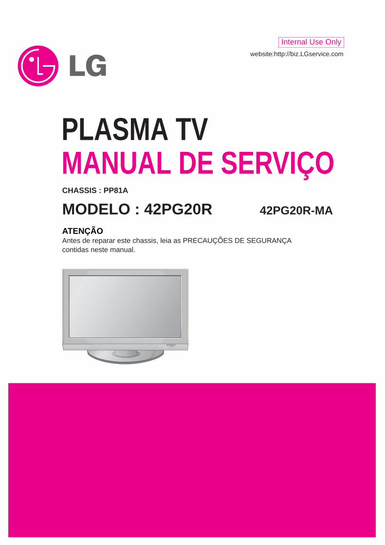
PLASMA TVMANUAL DE SERVIÇO
ATENÇÃOAntes de reparar este chassis, leia as PRECAUÇÕES DE SEGURANÇAcontidas neste manual.
CHASSIS : PP81A
MODELO : 42PG20R 42PG20R-MA
website:http://biz.LGservice.com
Internal Use Only
CHVOLMENUINPUT ENTER
- 2 -Copyright © 2007 LG Electronics. Inc. All right reserved. Only for training and service purposes
LGE Internal Use Only
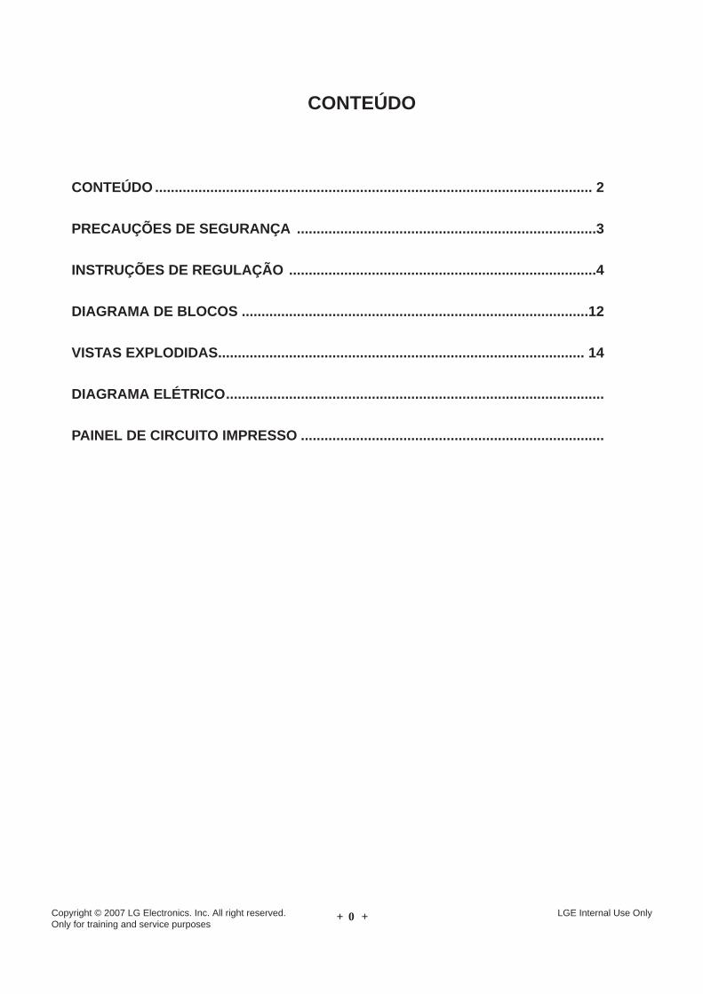
CONTEÚDO
CONTEÚDO ............................................................................................................... 2
PRECAUÇÕES DE SEGURANÇA ............................................................................3
INSTRUÇÕES DE REGULAÇÃO ..............................................................................4
DIAGRAMA DE BLOCOS ........................................................................................12
VISTAS EXPLODIDAS............................................................................................. 14
DIAGRAMA ELÉTRICO................................................................................................
PAINEL DE CIRCUITO IMPRESSO .............................................................................

- 3 -Copyright © 2007 LG Electronics. Inc. All right reserved. Only for training and service purposes
LGE Internal Use Only
PRECAUÇÕES DE SEGURANÇA
ADVERTÊNCIA : Antes de reparar este chassis., leia as “ PRECAUÇÕES DE RADIAÇÃO POR RAIO X “, “ INSTRUÇÕESDE SEGURANÇA “ e “ AVISO SOBRE SEGURANÇA DE PRODUTOS “.
Muitas partes elétricas e mecânicas neste chassis, tem características relacionadas com a segurança. Estas característicasfrequentemente não são verificadas nas inspeções visuais e a proteção que proporcionam contra a RADIAÇÃO DE RAIO “ X “ nemsempre se obtem utilizando componente com maior potência ou de maior isolação. As peças que têm essas características desegurança são identificadas por uma marca [ ] impressa sobre o diagrama esquemático e a marca [ ★ ] impressa na lista departes elétricas. Antes de substituir algum destes componentes, leia cuidadosamente este manual. O uso de peças de reposição quenão tenham as mesmas características de segurança, como especificado na lista de material de reposição, pode gerar Radiação deRaios “X”.
1. Quando o receptor está em operação, são geradas tensõespotencialmente altas em torno de 25-29 kV. Operar o receptorfora de seu gabinete ou com a tampa traseira removida podecausar perigo de choque elétrico. (1) Ninguém deverá tentar reparar o aparelho sem estarfamiliarizado com as precauções que são necessáriasquando se trabalha com um equipamento de alta tensão. (2) Sempre descarregue o anodo do cinescópio ao terra paraevitar o risco de choque elétrico antes de remover o conectordo anodo (chupeta de alta tensão). (3) Descarregue completamente o potencial do cinescópioantes de manuseá-lo. O cinescópio é de alto vácuo, e sequebrar, os fragmentos de vidro são expelidos violentamente.
2. S e queimar algúm fusível deste receptor de televisão,substitua-o por outro especificado na lista de peças elétricas.
3. Quando substituir placas de circuito impresso ou módulos, fixeseus fios nos terminais antes de soldar.
4. Quando substituir uma resistência de potência (resistor depelícula de óxido metálico) no painel de circuito impresso,mantenha os seus terminais com 10mm de distância dopainel.
5. Mantenha os fios e cabos distantes de componentes de altapotência e de alta temperatura.
6. Este receptor deve operar em redes de 100 a 240 V AC.7. Antes de devolver este aparelho ao cliente, faça uma
verificação de fuga de corrente sobre as partes metálicasexpostas do gabinete, tais com antenas, terminais, cabeçasde parafusos, tampas de metal, alavancas de controle, etc., ecertifique-se de que o aparelho funciona sem perigo dechoque elétrico. Ligue o cabo de rede do aparelhodiretamente a uma tomada de força de 100-240 V AC. Não
utilize um transformador de isolação durante este teste.Uti l ize um voltímetro de no mínimo 1KW por Volt desensibilidade, da forma que se segue. Quando a unidade estiver conectada ao AC, pulse ocomutador primeiramente em “ON” (ligado) e em seguida em“OFF” (desligado), meça desde um ponto de terra conhecido(tal como um terminal de terra central da rede elétrica) atodas as partes metálicas expostas do televisor ( antenas,teclas metálicas, capas metálicas, alavancas de controle,etc..) especialmente qualquer parte metálica que possaoferecer um caminho ao chassis. Nenhuma medição decorrente elétrica deve exceder 0,5 mA. Repita a provamudando a posição do pluque de rede na tomada AC.Qualquer medição que não esteja dentro dos limites aquiespecificados, representam risco potencial de choque elétrico que deve ser sanado antes que o aparelho retorne aocliente.
INSTRUÇÕES DE SEGURANÇA
AVISO SOBRE SEGURANÇA DE PRODUTO
DEVICEUNDERTEST
TEST ALLEXPOSED MET AL
SURFACES
2-WIRE CORD
ALSO TEST WITHPLUG REVERSED(USING AC ADAPTERPLUG AS REQUIRED)
EAR THGROUND
LEAKAGECURRENTTESTER
(READING SHOULDNO T BE ABOVE
0.5mA)
+-
Aparelhoa serexaminado
Probadorde fuga decorriente
A leitura não deveexceder 0.5mA
Prove todas assuperficiesmetálicas
Também prove como plugue de redeinvertendo apolaridade
Terra
- 4 -Copyright © 2007 LG Electronics. Inc. All right reserved. Only for training and service purposes
LGE Internal Use Only
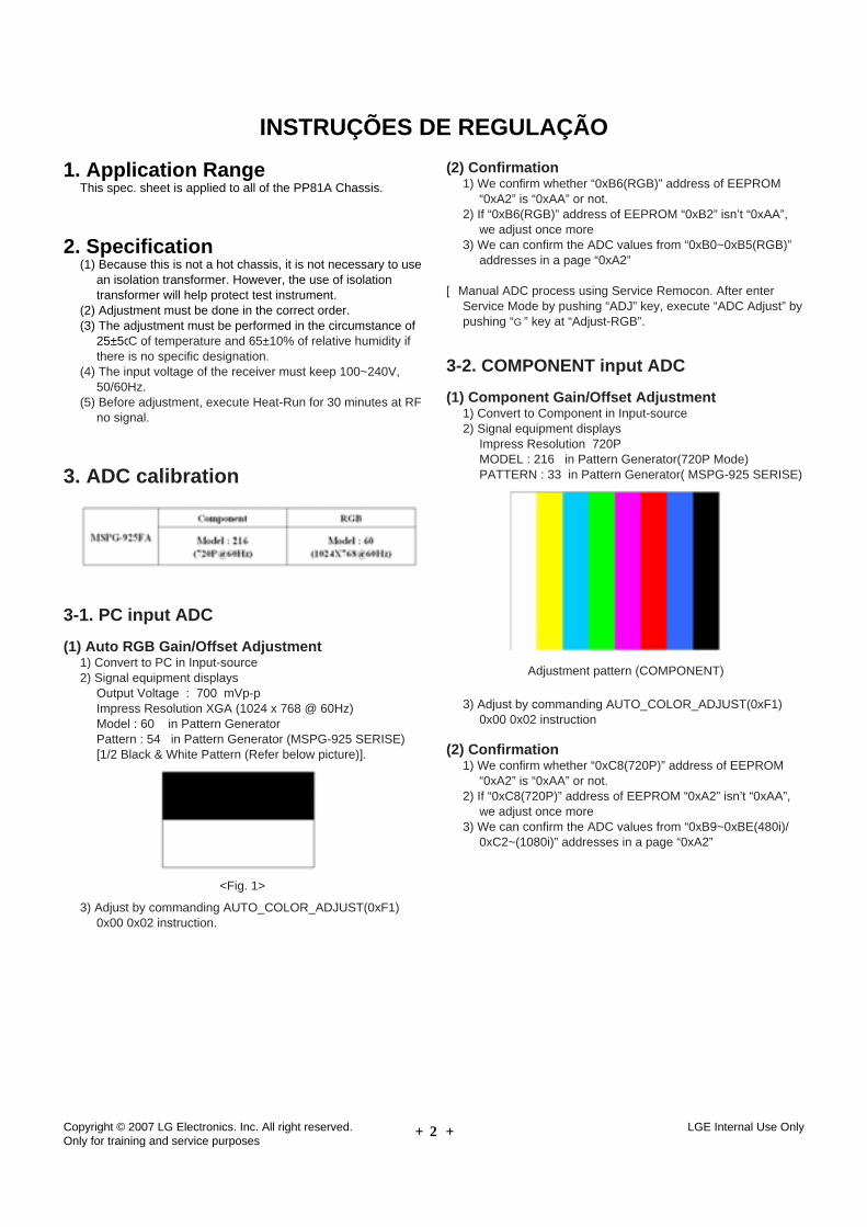
INSTRUÇÕES DE REGULAÇÃO
1. Application RangeThis spec. sheet is applied to all of the PP81A Chassis.
2. Specification(1) Because this is not a hot chassis, it is not necessary to use
an isolation transformer. However, the use of isolationtransformer will help protect test instrument.
(2) Adjustment must be done in the correct order.(3) The adjustment must be performed in the circumstance of
25±5cC of temperature and 65±10% of relative humidity ifthere is no specific designation.
(4) The input voltage of the receiver must keep 100~240V,50/60Hz.
(5) Before adjustment, execute Heat-Run for 30 minutes at RFno signal.
3. ADC calibration
3-1. PC input ADC
(1) Auto RGB Gain/Offset Adjustment1) Convert to PC in Input-source2) Signal equipment displays
Output Voltage : 700 mVp-pImpress Resolution XGA (1024 x 768 @ 60Hz)Model : 60 in Pattern GeneratorPattern : 54 in Pattern Generator (MSPG-925 SERISE) [1/2 Black & White Pattern (Refer below picture)].
3) Adjust by commanding AUTO_COLOR_ADJUST(0xF1)0x00 0x02 instruction.
(2) Confirmation1) We confirm whether “0xB6(RGB)” address of EEPROM
“0xA2” is “0xAA” or not. 2) If “0xB6(RGB)” address of EEPROM “0xB2” isn’t “0xAA”,
we adjust once more3) We can confirm the ADC values from “0xB0~0xB5(RGB)”
addresses in a page “0xA2”
[ Manual ADC process using Service Remocon. After enterService Mode by pushing “ADJ” key, execute “ADC Adjust” bypushing “G” key at “Adjust-RGB”.
3-2. COMPONENT input ADC
(1) Component Gain/Offset Adjustment1) Convert to Component in Input-source2) Signal equipment displays
Impress Resolution 720PMODEL : 216 in Pattern Generator(720P Mode)PATTERN : 33 in Pattern Generator( MSPG-925 SERISE)
3) Adjust by commanding AUTO_COLOR_ADJUST(0xF1)0x00 0x02 instruction
(2) Confirmation1) We confirm whether “0xC8(720P)” address of EEPROM
“0xA2” is “0xAA” or not. 2) If “0xC8(720P)” address of EEPROM “0xA2” isn’t “0xAA”,
we adjust once more3) We can confirm the ADC values from “0xB9~0xBE(480i)/
0xC2~(1080i)” addresses in a page “0xA2”
<Fig. 1>
Adjustment pattern (COMPONENT)

- 5 -Copyright © 2007 LG Electronics. Inc. All right reserved. Only for training and service purposes
LGE Internal Use Only
4. PCB Assembly Adjustment Items
4-1. Option Adjustment Following BOM Tool Option1 Tool Option2Area Option
* Profile: Must be changed the option value because beingdifferent with some setting value depend on module, inchand market
* Equipment : Adjustment Remote Controller
(1) Push the IN-START key in the Adjust R/C.(2) Input the Option Number that was specified in the BOM,
into the Shipping area.(3) Select “Tool Option1/ Tool Option2/ Area Option” by using
D /E (CH+/-) key, and press the number key(0~9)consecutivelyex) If the value of Tool Option1 is 7, input the data using
number key “7” (Fig. 2)
Caution: Don’t Push “IN-STOP” key after PCB assemblyadjustment.
(4) Adjustment method Before PCBA check, have to change the Tool option andArea option
[ About PDPAfter done all adjustments, Press IN-START button andcompare Tool option and Area option value with its BOM, if itis correctly same then Change “RF mode” and then unplugthe AC cable.If it is not same, then correct it same with BOM and unplug ACcable. For correct it to the model°Øs module from factory JIG model.
[ Don’t push The IN-STOP KEY after completing the functioninspection.
5. S/W Program Download
5-1. ProfileThis is for downloading the s/w to the flash memory of theIC803
5-2. Equipment (1) PC(2) ISP_tool program(3) Download jig
5-3. Connection Structure
5-4. Connection Condition(1) IC name and circuit number : Flash Memory and IC803(2) Use voltage : 3.3V (5 pin)(3) SCL : 15 pin(4) SDA : 12 pin(5) Tact time : about 2min and 30seconds
6. Download Method (PCB Ass’y)
6-1. Preliminary Steps
(1) Connect the download jig to D-sub jack
(2) Connect the PC to USB jack
<Fig. 2>
- 6 -Copyright © 2007 LG Electronics. Inc. All right reserved. Only for training and service purposes
LGE Internal Use Only
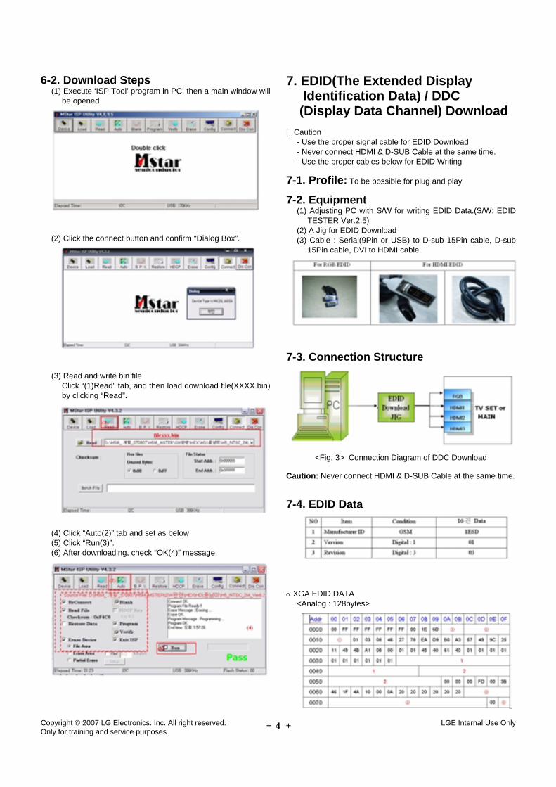
6-2. Download Steps(1) Execute ‘ISP Tool’ program in PC, then a main window will
be opened
(2) Click the connect button and confirm “Dialog Box”.
(3) Read and write bin fileClick “(1)Read” tab, and then load download file(XXXX.bin)by clicking “Read”.
(4) Click “Auto(2)” tab and set as below(5) Click “Run(3)”.(6) After downloading, check “OK(4)” message.
7. EDID(The Extended DisplayIdentification Data) / DDC(Display Data Channel) Download
[ Caution- Use the proper signal cable for EDID Download- Never connect HDMI & D-SUB Cable at the same time.- Use the proper cables below for EDID Writing
7-1. Profile: To be possible for plug and play
7-2. Equipment(1) Adjusting PC with S/W for writing EDID Data.(S/W: EDID
TESTER Ver.2.5)(2) A Jig for EDID Download(3) Cable : Serial(9Pin or USB) to D-sub 15Pin cable, D-sub
15Pin cable, DVI to HDMI cable.
7-3. Connection Structure
Caution: Never connect HDMI & D-SUB Cable at the same time.
7-4. EDID Data
O XGA EDID DATA<Analog : 128bytes>
<Fig. 3> Connection Diagram of DDC Download

- 7 -Copyright © 2007 LG Electronics. Inc. All right reserved. Only for training and service purposes
LGE Internal Use Only
<HDMI 1 : 256bytes>
<HDMI 2 : 256bytes>
<HDMI 3 : 256bytes>
O Detail EDID Options are below (ⓐ, ⓑ, ⓒ, ⓓ, ⓔ)
ⓐ Product ID
ⓑ Serial No=> Controlled on production line
ⓒ Month, Year=> Controlled on production line:
ex) Monthly: ‘11’ -> ‘0B’ Year: ‘2007’ -> ‘11’
ⓓ Model Name(Hex)
ⓔ Checksum=> Changeable by total EDID data
1) 42inch Model
2) 50/60inch Model

- 8 -Copyright © 2007 LG Electronics. Inc. All right reserved. Only for training and service purposes
LGE Internal Use Only
7-5. Preparation for Adjustment(1) As above Fig. 3, Connect the Set, EDID Download Jig,,
PC & Cable(2) Turn on the PC & EDID Download Jig. And Execute the
S/W : EDID TESTER Ver.2.5(3) Set up the S/W option
Repeat Number : 5Device Address : A0PageByte : 8
(4) Power on the Set
1) Sequence of Adjustment
1. DDC data of Analog-RGB(1) Init the data
(2) Load the EDID data.(Open File).
(3) Set the S/W as below.
(4) Push the “Write Data & Verify” button. And confirm “Yes”.
(5) If the writing is finished, you will see the “OK” message.
8. HDCP(High-Bandwidth Digital Contents Protection)(1) Connect D-sub Signal Cable to D-Sub Jack(2) Input HDCP key with HDCP-key- in-program(3) HDCP Key value is stored on Main M-STAR
IC(LGE6891DD) which is 0x80~0x90 addresses of0x00~0x01 page(EEPROM MAP PAGE0~PAGE1 / START:A080)
(4) Play the Equipment(DVD Player) included HDCP Key andconfirm whether picture is displayed or not of using DVDPlayer.
(5) HDCP Key value is different among the sets
- 9 -Copyright © 2007 LG Electronics. Inc. All right reserved. Only for training and service purposes
LGE Internal Use Only
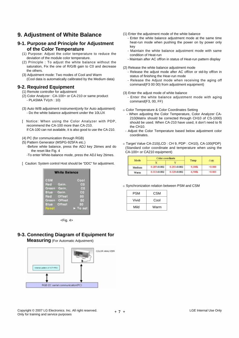
9. Adjustment of White Balance
9-1. Purpose and Principle for Adjustment of the Color Temperature
(1) Purpose: Adjust the color temperature to reduce thedeviation of the module color temperature.
(2) Principle : To adjust the white balance without thesaturation, Fix the one of R/G/B gain to C0 and decreasethe others.
(3) Adjustment mode: Two modes of Cool and Warm(Cool data is automatically calibrated by the Medium data)
9-2. Required Equipment(1) Remote controller for adjustment (2) Color Analyzer : CA-100+ or CA-210 or same product
- PLASMA TV(ch : 10)
(3) Auto W/B adjustment instrument(only for Auto adjustment)- Do the white balance adjustment under the 10LUX
[ Notice: When using the Color Analyzer with PDP,recommend the CA-100 more than CA-210.If CA-100 can not available, it is also good to use the CA-210.
(4) PC (for communication through RGB) (5) Pattern Generator (MSPG-925FA etc.)
-Before white balance, press the ADJ key 2times and dothe reset like Fig. 4
-To enter White-balance mode, press the ADJ key 2times.
[ Caution: System control Host should be “DDC” for adjustment.
9-3. Connecting Diagram of Equipment for Measuring (For Automatic Adjustment)
(1) Enter the adjustment mode of the white balance- Enter the white balance adjustment mode at the same time
heat-run mode when pushing the power on by power onlykey
- Maintain the white balance adjustment mode with samecondition of Heat-run
- Maintain after AC off/on in status of Heat-run pattern display
(2) Release the white balance adjustment mode- Release the adjust mode after AC off/on or std-by off/on in
status of finishing the Hear-run mode- Release the Adjust mode when receiving the aging off
command(F3 00 00) from adjustment equipment)
(3) Enter the adjust mode of white balance- Enter the white balance adjustment mode with aging
command(F3, 00, FF)
O Color Temperature & Color Coordinates Setting- When adjusting the Color Temperature, Color Analyzer CA-
210(Matrix should be corrected through CH10 of CS-1000)should be used. When CA-210 have used, it don’t need to fitthe CH10.
- Adjust the Color Temperature based below adjustment colorcoordinates.
O Target Value CA-210(LCD : CH 9, PDP : CH10), CA-100(PDP)(Standard color coordinate and temperature when using theCA-100+ or CA210 equipment)
O Synchronization relation between PSM and CSM
<Fig. 4>
PSM
Vivid
Mild
CSM
Cool
Warm

- 10 -Copyright © 2007 LG Electronics. Inc. All right reserved. Only for training and service purposes
LGE Internal Use Only
O DDC Adjustment Command Set
[ R/G/B GAIN max value : C0
Adjustment
Adjustment
Adjustment
- 11 -Copyright © 2007 LG Electronics. Inc. All right reserved. Only for training and service purposes
LGE Internal Use Only
9-4. Adjustment of White Balance for Manual Adjustment
Adjustment mode: Two modes of Medium(Vivid) and Warm(Cool data is automatically calibrated by the Medium data)
- Equipment : 1) Color analyzer(CA100+, CA210) should beused in the calibrated ch by CS-1000(.(LCD :CH9, PDP : CH10)
2) Adjustment remocon
- For manual adjustment, it is also possible by the followingsequence.Operate the zero-calibration of the CA-100+ or CA-210, thenstick sensor to the module when adjusting.
(1) Select white pattern of heat-run by pressing “POWER ON”key on remote control for adjustment then operate heat runlonger than 15 minutes. (recommend) (If not executed this step, the condition for W/B will bedifferent)
(2) Changing to the AV mode by remote control.(Push front-AV)
(3) Input external pattern(85% white pattern).(4) Stick sensor to center of the screen and select each items
(Red/Green/Blue Gain and Offset) using D/E(CH +/-) keyon R/C..
(5) Adjust R/ G/B Gain using F/G(VOL +/-) key on R/C.(6) Adjust two modes of Medium(Vivid) and Warm as below
figure.(Fix the one of R/G/B and change the others)1) Default : Medium(Vivid)2) Push the “VOL +” key twice : Warm
[ Refer to the below case to know what value is fixed.
[CASE]First adjust the coordinate much away from the target value(x, y).
1. x, y > target1) Decrease the R, G.
2. x, y < target1) First decrease the B gain, 2) Decrease the one of the others.
- In case of decreasing the x, decreasing the R : fix G- In case of decreasing the y , decreasing the G : fix R
3. x > target , y < target1) First decrease B, so make y a little more than the target.2) Adjust x value by decreasing the R
4. x < target , y > target1) First decrease B, so make x a little more than the target.2) Adjust x value by decreasing the G
(7) When adjustment is completed, Exit adjustment modeusing EXIT key on R/C.
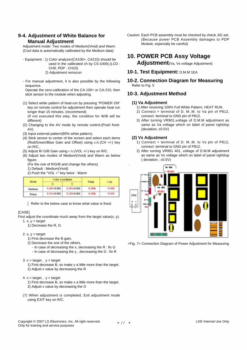
Caution: Each PCB assembly must be checked by check JIG set.(Because power PCB Assembly damages to PDPModule, especially be careful)
10. POWER PCB Assy VoltageAdjustment(Va, Vs voltage Adjustment)
10-1. Test Equipment: D.M.M 1EA
10-2. Connection Diagram for MeasuringRefer to Fig. 5
10-3. Adjustment Method
(1) Va Adjustment1) After receiving 100% Full White Pattern, HEAT RUN.2) Connect + terminal of D. M..M. to Va pin of P812,
connect -terminal to GND pin of P812.3) After turning VR901,voltage of D.M.M adjustment as
same as Va voltage which on label of panel right/top(deviation; ±0.5V)
(2) Vs Adjustment1) Connect + terminal of D. M..M. to Vs pin of P812,
connect -terminal to GND pin of P812.2) After turning VR951 401, voltage of D.M.M adjustment
as same as Vs voltage which on label of panel right/top( deviation ; ±0.5V)
<Fig. 7> Connection Diagram of Power Adjustment for Measuring
- 12 -Copyright © 2007 LG Electronics. Inc. All right reserved. Only for training and service purposes
LGE Internal Use Only
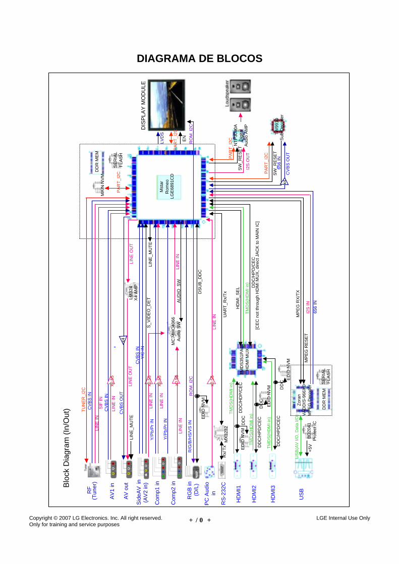
DIAGRAMA DE BLOCOSB
lock
Dia
gram
(In
/Out
)
AV
1 in
Sid
eAV
in(A
V2
in)
Com
p1 in
Com
p2 in
RG
B in
(D/L
)
AV
out
CV
BS
IN
Y/P
b/P
r IN
R/G
/B/H
S/V
S IN
CV
BS
IN
LIN
E O
UT
LIN
E IN
LIN
E_M
UT
E
RS
-232
CR
x/T
xM
X32
32
RF
(Tun
er)
PC
Aud
ioin
DIS
PLA
Y M
OD
ULE
ED
ID N
VM
ED
ID N
VM
HD
MI1
HD
MI2
HD
MI3
US
B
TM
DS
351P
AG
HD
MI M
UX
Zor
anV
AD
DIS
-966
XD
MP
EG
Dec
oder
DD
R M
EM
DD
R M
EM
SE
RIA
LF
LAS
H
Mst
arR
omeo
LGE
6891
CD
TW
9910
Sub
Dec
oder
NT
P30
00A
Dig
ital
Aud
io A
MP
MA
IN N
VM
MC
74H
C40
66A
udio
SW
LM32
4X
4 A
MP
SE
RIA
LF
LAS
H
BD
2041
Pro
tect
IC
ED
ID N
VM
DD
C/H
DP
/CE
C
TM
DS
(HD
MI i
n)
DD
C/H
PD
/CE
C
TM
DS
(HD
MI i
n)
TM
DS
(HD
MI i
n)
US
B(A
V I/
O, D
ata
I/O)
+5V
CV
BS
OU
T
656
INS
W_R
ES
ET
PA
RT
_I2CPA
RT
_I2C
SW
_RE
SE
T
I2S
OU
T
PA
RT
_I2C
LVD
S
EN
MP
EG
RX
/TX
MP
EG
RE
SE
TI2
S IN
656
IN
TM
DS
(HD
MI i
n)
DD
C/H
PD
/CE
C
DD
C/H
PD
/CE
C[C
EC
not
thro
ugh
HD
MI M
UX
, dire
ct J
AC
K to
MA
IN IC
]
DD
C
DD
C
DD
C
UA
RT
_Rx/
Tx
AU
DIO
_SW
LIN
E IN
LIN
E IN
LIN
E IN
Y/P
b/P
r IN
LIN
E IN
Y/C
IN
LIN
E IN
ED
ID N
VM
RO
M_I
2C
DS
UB
_DD
C
x0.5
5
x0.5
5
x0.5
5
x0.5
5S
_VID
EO
_DE
TLI
NE
_MU
TE
LIN
E O
UT
CV
BS
OU
Tx4
x4
x0.5
5LI
NE
IN
CV
BS
INS
IF IN
TU
NE
R_I
2C
PA
RT
_I2C
RO
M_I
2C
HD
MI_
SE
L

- 13 -Copyright © 2007 LG Electronics. Inc. All right reserved. Only for training and service purposes
LGE Internal Use Only
Blo
ck D
iagr
am (
I2C
& C
omm
unic
atio
n Li
ne)
AV
1 in
Sid
eAV
in(A
V2
in)
Com
p1 in
Com
p2 in
RG
B in
(D/L
)
AV
out
CV
BS
IN
Y/P
b/P
r IN
R/G
/B/H
S/V
S IN
CV
BS
IN
LIN
E O
UT
LIN
EIN
LIN
E_M
UT
E
RS
-232
CR
x/T
xM
X32
32
RF
(Tun
er)
PC
Aud
ioin
DIS
PLA
Y M
OD
ULE
ED
ID N
VM
ED
ID N
VM
HD
MI1
HD
MI2
HD
MI3
US
B
TM
DS
351P
AG
HD
MI M
UX
Zor
anV
AD
DIS
-966
XD
MP
EG
Dec
oder
DD
R M
EM
DD
R M
EM
SE
RIA
LF
LAS
H
Mst
arR
omeo
LGE
6891
CD
TW
9910
Sub
Dec
oder
NT
P30
00A
Dig
ital
Aud
io A
MP
MA
IN N
VM
MC
74H
C40
66A
udio
SW
LM32
4X
4 A
MP
SE
RIA
LF
LAS
H
BD
2041
Pro
tect
IC
ED
ID N
VM
DD
C/H
DP
/CE
C
TM
DS
(HD
MI i
n)
DD
C/H
PD
/CE
C
TM
DS
(HD
MI i
n)
TM
DS
(HD
MI i
n)
US
B(A
V I/
O, D
ata
I/O)
+5V
CV
BS
OU
T
656
INS
W_R
ES
ET
PA
RT
_I2CPA
RT
_I2C
SW
_RE
SE
T
I2S
OU
T
PA
RT
_I2C
LVD
S
EN
MP
EG
RX
/TX
MP
EG
RE
SE
TI2
S IN
656
IN
TM
DS
(HD
MI i
n)
DD
C/H
PD
/CE
C
DD
C/H
PD
/CE
C[C
EC
not
thro
ugh
HD
MI M
UX
, dire
ct J
AC
K to
MA
IN IC
]
DD
C
DD
C
DD
C
UA
RT
_Rx/
Tx
AU
DIO
_SW
LIN
EIN
LIN
EIN
LIN
EIN
Y/P
b/P
r IN
LIN
EIN
Y/C
IN
LIN
EIN
ED
ID N
VM
RO
M_I
2C
DS
UB
_DD
C
x0.5
5
x0.5
5
x0.5
5
x0.5
5S
_VID
EO
_DE
TLI
NE
_MU
TE
LIN
E O
UT
CV
BS
OU
Tx4
x4
x0.5
5LI
NE
IN
CV
BS
INS
IF IN
TU
NE
R_I
2C
PA
RT
_I2C
RO
M_I
2C
HD
MI_
SE
L

- 14 -Copyright © 2007 LG Electronics. Inc. All right reserved. Only for training and service purposes
LGE Internal Use Only
VISTAS EXPLODIDAS
A2
300
305
302
200
202
560
571 120
561
570 301
260
590 501
270 603
520
203240
205
204
206
250 602
601
580
900
400
201
303304
306
Many electrical and mechanical parts in this chassis have special safety-related characteristics. Theseparts are identified by in the Schematic Diagram and EXPLODED VIEW. It is essential that these special safety parts should be replaced with the same components asrecommended in this manual to prevent X-RADIATION, Shock, Fire, or other Hazards. Do not modify the original design without permission of manufacturer.
IMPORTANT SAFETY NOTICE

Copyright © 2008 LG Electronics. Inc. All right reserved. Only for training and service purposes
LGE Internal Use Only

Copyright © 2008 LG Electronics. Inc. All right reserved. Only for training and service purposes
LGE Internal Use Only
Copyright © 2008 LG Electronics. Inc. All right reserved. Only for training and service purposes
LGE Internal Use Only
Copyright © 2008 LG Electronics. Inc. All right reserved. Only for training and service purposes
LGE Internal Use Only
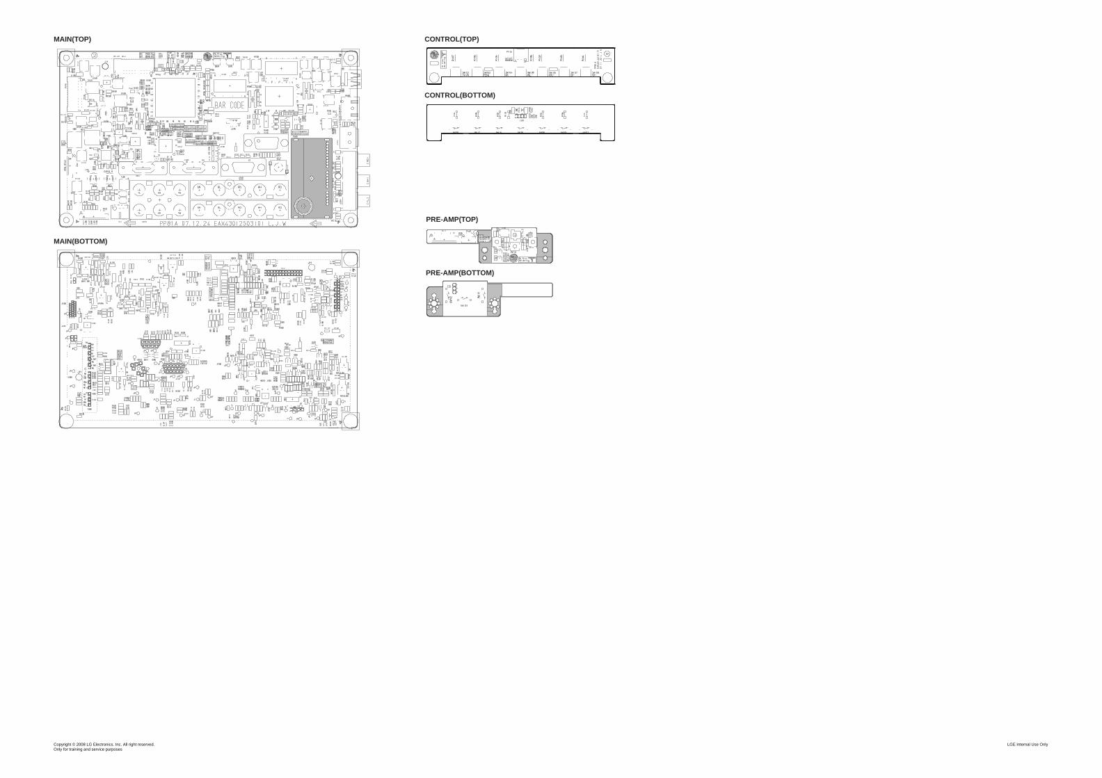
MAIN(TOP)
MAIN(BOTTOM)
CONTROL(TOP)
CONTROL(BOTTOM)
PRE-AMP(TOP)
PRE-AMP(BOTTOM)
Depto de Assistência TécnicaAv. D. Pedro I, W7777 - Distrito IndustrialPiracangagua II - Taubaté - SP - BrasilCx. Postal 324 - CEP 12.010-970Tel. : (012) 221-8555 Fax. : (012)221-8550
Jan., 2008Printed in KoreaP/NO : MFL41859303
LG Electronics Inc.


![LG SECURITY SYSTEM1]--LG...LG SECURITY SYSTEM LG uses the up-to-date technology that will fulfill your surveillance needs, anytime or anywhere. Rely on LG to protect what is important](https://img.pdfslide.us/doc/110x75/60b48bb772fcf26f42572741/lg-security-system-1-lg-lg-security-system-lg-uses-the-up-to-date-technology.jpg)