Embed Size (px)
Citation preview

1200 IEEE TRANSACTIONS ON POWER ELECTRONICS, VOL. 35, NO. 2, FEBRUARY 2020
Letters
Subtraction-Mode Switched-Capacitor ConvertersWith Parasitic Loss Reduction
Junmin Jiang , Member, IEEE, Xun Liu , Member, IEEE, Cheng Huang, Member, IEEE,Wing-Hung Ki, Member, IEEE, Philip K. T. Mok , Fellow, IEEE, and Yan Lu , Senior Member, IEEE
Abstract—In this letter, subtraction-mode switched-capacitor(SC) converters are proposed and analyzed. When compared toa conventional summation-mode SC converter, some of the flyingcapacitors of the subtraction-mode SC converters have reducedvoltage swings, and hence the switching loss of the correspondingpositive- and negative-plate parasitic capacitors is reduced, andefficiency is enhanced. The proposed subtraction-mode topologiesuse the same number of flying capacitors and switches as thesummation-mode topologies, and they are reconfigured withoutusing any auxiliary circuits, so there are no tradeoffs in terms ofpower density, cost, voltage conversion ratio (VCR), or equivalentoutput resistance. A test chip with VCRs of 1/3×, 2/3×, 3/4×,and 4/5× was fabricated in a 65-nm CMOS process. Efficiencyimprovement of more than 10% was achieved when compared tosummation-mode designs.
I. INTRODUCTION
FULLY integrated switched-capacitor (SC) converters aregaining demands in emerging applications such as low-
power Internet-of-Things and system-on-chips. For low-powerapplications, capacitors are readily integrated on-chip, such thatsystem form factor and cost are reduced. For fully integrated SCconverters, power density, and efficiency are the important con-siderations, because they have direct impact on the standby timeand the silicon area. A standard CMOS process has low on-chipcapacitance density, and very high switching frequency (tens tohundreds of MHz) is used to reduce the output impedance andincrease the power density, and results in high switching andparasitic loss, and degrades efficiency significantly.
Metal-oxide-semiconductor (MOS) capacitors are usuallyused in fully integrated SC converters, as they have the highest
Manuscript received July 6, 2019; accepted August 3, 2019. Date of publi-cation August 5, 2019; date of current version November 12, 2019. This workwas supported by the Research Grants Council of the Theme-Based ResearchScheme of Hong Kong under Project T23-612/12-R. (Corresponding author:Junmin Jiang.)
J. Jiang, X. Liu, W.-H. Ki, and P. K. T. Mok are with the Department ofElectronic and Computer Engineering, The Hong Kong University of Scienceand Technology, Hong Kong, China (e-mail: [email protected]; [email protected]; [email protected]; [email protected]).
C. Huang is with the ECpE Department, Iowa State University, Ames, IA50011 USA (e-mail: [email protected]).
Y. Lu is with the State Key Laboratory of Analog Mixed Signal and VLSI,Institute of Microelectronics, and also with FST-ECE, University of Macau,Macao, China (e-mail: [email protected]).
Color versions of one or more of the figures in this letter are available onlineat http://ieeexplore.ieee.org.
Digital Object Identifier 10.1109/TPEL.2019.2933623
Fig. 1. Top- and bottom-plate parasitic capacitors of on-chip MOS capacitors.
capacitance density among all on-chip capacitors, but they alsohave the largest parasitic capacitors. Fig. 1 shows two commonlyused MOS capacitors: the NCAP and the PMOS capacitors.For the NCAP, the top-plate is the gate and the bottom-plateis the source/drain, and the main capacitor is Cg . The junctionfrom P-substrate to N-well should be reverse-biased, formingthe parasitic capacitor CW across the junction JW . P-substrateis connected to ground, and CW will be charged and dischargedas Cg switches and introduces parasitic loss. Similarly, for thePMOS capacitor, there are parasitic capacitors CP and CW
across the diodes from drain/source to the N-well and the N-wellto the P-substrate. These parasitic capacitors (CP and CW ) arearound 3%–5% of the gate capacitance. Junction capacitorsare determined by doping concentrations of P-substrate andN-well, and stay relatively constant across different technologynodes. Hence, parasitic loss is quite significant as the operatingfrequency increases.
Special techniques in achieving high capacitance density werereported, such as deep-trench capacitors [1], ferroelectric capac-itors [2], and high-density MIM capacitors, but additional andcostly processing steps are needed. An alternative method toreduce parasitic loss could be clever circuit design.
In CMOS process, the parasitic capacitance is voltage depen-dent on the body bias voltage. In [3] and [4], the N-wells ofthe MOS capacitors are left floating with a high impedance toground or supply voltage, and the two parasitic capacitors areconnected in series with respect to the substrate. If the N-wellsare reverse-biased, then increasing the bias voltage reduces the
0885-8993 © 2019 IEEE. Personal use is permitted, but republication/redistribution requires IEEE permission.See http://www.ieee.org/publications_standards/publications/rights/index.html for more information.
Authorized licensed use limited to: Universidade de Macau. Downloaded on July 02,2020 at 03:13:52 UTC from IEEE Xplore. Restrictions apply.

IEEE TRANSACTIONS ON POWER ELECTRONICS, VOL. 35, NO. 2, FEBRUARY 2020 1201
Fig. 2. Operating principle of (a) summation modes and (b) subtraction modes.
junction capacitance, and the high bias voltage can be generatedfrom an on-chip doubler [5] or an external voltage supply [6].All the above methods require auxiliary power supplies and extracircuitry, which introduce extra cost. Besides, when the voltageconversion ratio (VCR) is small, the flying capacitors have largervoltage swings, and so do the corresponding parasitic capacitors,thus still incurring larger parasitic loss.
In this letter, we propose subtraction-mode SC converters thatuse the same number of flying capacitors and switches to achievethe same VCRs and output resistances, with flying capacitorshaving smaller voltage swings that result in lower parasitic loss.A test chip with both summation mode and subtraction mode infour commonly used VCRs: 1/3×, 2/3×, 3/4×, and 4/5× wasfabricated, for comparison.
II. PROPOSED SUBTRACTION-MODE SC CONVERTERS
A. Summation-Mode Series-Parallel Topologies
Series-parallel topologies are the most commonly usedtopologies in state-of-the-art step-down SC converters. Fig. 2(a)shows the steady-state operations of SC converters with fourtypical VCRs (1/3×, 2/3×, 3/4×, and 4/5×). Take the 1/3×SC converter as an example, and consider the load current isnegligible. In Φ2 (the series phase), two flying capacitors C1
and C2 and the loading capacitor CL are connected in series andcharged up by the supply voltage VIN, and we have
Φ2 : VIN − VO = VC2 + VC1. (1)
In Φ1 (the parallel phase), C1, C2, and CL are connected inparallel and all are discharged by load current, and
Φ1 : VC2 = VC1 = VO. (2)
Fig. 3. Operating principle of general (a) 1/(N + 1)× and (b) N/(N + 1)× SCconverters.
Solving (1) and (2) gives VO = VC1 = VC2 = 1/3VIN.The above operations extend to similar 1/(N+ 1)× and N(N+
1)× converters (N is flying capacitor numbers), as shown in Fig.3(a). Note that in the parallel phase (Φ1), all N flying capacitorsare connected in parallel so they have same dc voltage 1/(N +1) × VIN. Then, in the series phase (Φ2), all N flying capacitorsCi(i = 1 . . . N) are stacked in series with the positive-plate ofCi connected to the negative-plate of Cj , such that the voltageacross all Ci in series is the “sum” of all capacitor voltages, andthis is the reason of the name “summation mode.” Clearly, forC1, the voltage swing of the positive-plate and negative-plate isN/(N + 1) × VIN, and subsequent Ci has lower voltage swings.Hence, the parasitic capacitors of C1 contribute the most to theparasitic loss.
B. Subtraction-Mode Topologies
Next, we propose an alternative method to generate step-downVCRs (1/3×, 2/3×, 3/4×, and 4/5×) as shown in Fig. 2(b).Again, take the 1/3× SC converter as an example. In Ф1, C1 isconnected in series to the parallel-connected C2 and CL, and
Φ1 : VIN = VC2 + VC1 = VC1 + VO. (3)
In Ф2, the negative-plate of C1 is connected to ground, andthe positive-plate is connected to C2 (with a reversed polarity)and CL in series, and
Φ2 : VC1 = VC2 + VO ⇒ VO = VC1 − VC2. (4)
Solving (3) and (4) givesVO = 1/3VIN. Note that in the seriesphase (Ф2), when C1 and C2 are viewed as connected in series,plates of the same polarity are connected together, such that thevoltage across the two capacitors is the “difference” of theircapacitor voltages, and hence the name of “subtraction mode.”Fig. 2(b) shows the subtraction-mode converters with VCRs of2/3×, 3/4×, and 4/5×, and their output voltages are
VO,2/3× = VIN − (VC2 − VC1) = 2/3VIN. (5)
VO,3/4× = VIN − (VC3 −VC2 −VC1) = 3/4VIN. (6)
VO,4/5× = VIN − (VC4 − VC3 − VC2 −VC1) = 4/5VIN.(7)
Authorized licensed use limited to: Universidade de Macau. Downloaded on July 02,2020 at 03:13:52 UTC from IEEE Xplore. Restrictions apply.

1202 IEEE TRANSACTIONS ON POWER ELECTRONICS, VOL. 35, NO. 2, FEBRUARY 2020
TABLE ICOMPARISON OF VOLTAGE SWINGS OF EACH FLYING CAPACITOR
With no loss of generality, the flying capacitor that has thelargest capacitor voltage, which is also connected to VIN in oneof the phases, is labeled as C1 [see Fig. 2(b)].
To summarize, subtraction-mode SC converters with VCR= N/(N + 1) or 1/(N + 1) can be generated using N flyingcapacitors, as shown in Fig. 3(b). In one phase, C1 is chargedto VC1 = N/(N + 1)× VIN, while the other flying capacitorsCM (M �= 1) have VCM = 1/(N + 1) × VIN. In another phase,if the negative-plate of C1 is grounded, we have
VO = VC1 −∑
M �=1
VCM =1
N + 1VIN. (8)
And if positive-plate of C1 is connected to VIN, we have
VO = VIN −⎛
⎝VC1 −∑
M �=1
VCM
⎞
⎠ =N
N + 1VIN. (9)
For a subtraction-mode SC converter, C1 has a largerVC1, andthe voltage swings of its positive- and negative-plates (VC1+ andVC1−, respectively) are thus lower. In fact, ΔVC1+ and ΔVC1−are only 1/N of those of the summation mode counterparts.Table I summarizes the voltage swings of the positive- andnegative-plates of the flying capacitors of the converters inFig. 2. Recall that the parasitic capacitors of C1 contribute themost to the parasitic loss, and now they have much reducedvoltage swings, resulting in significant reduction of parasiticloss and improvement in efficiency. However, it should not behigher than the MOS’s breakdown voltage. The voltage swingsof the other flying capacitors remain the same in the two modes.
For two modes of SC converters, since the number of ca-pacitors and switches, and the charges through each capacitorsand switches are the same, steady-state performance such asthe equivalent output resistance remains the same. In summary,
Fig. 4. Parasitic capacitors on top- and bottom-plate of 1/3× mode.
subtraction-mode SC converters have lower parasitic loss, andno performance tradeoff in terms of power density.
III. ANALYSIS OF PARASITIC LOSS
We then turn to the analysis of reduction in parasitic loss. Weassume that the voltages of the flying capacitors are not affectedby the charge introduced by the parasitic capacitors, as they aremuch smaller (usually below 5%) than the flying capacitors. No-load condition is also assumed such that the capacitor voltagesdo not change from phase to phase.
Let us consider the 1/3× SC converter as shown in Fig. 4. Thepositive- and negative-plate parasitic capacitors areC1p+,C1p−,C2p+, and C2p−, and their voltage swings in both phases areindicated. For the summation-mode converter, whenФ1 changesto Ф2, C1p+ is charged from VO to VIN with a charge Q1P+.The energy sourced from VIN is
E1P+,CH =VINQ1P+ =VIN (VIN−VO)C1P+ =2
3V 2INC1P+.
(10)WhenФ2 changes toФ1, C1p+ is discharged from VIN to VO,
and the energy that is returned to VO is
E1P+,DIS =VOQ1P+ = VO (VIN − VO)C1P+ =2
9V 2INC1P+.
(11)The energy loss due to C1P+ is the difference of (10) and
(11), and is given by
E1P+,LOSS = E1P+,CH − E1P+,DIS =4
9V 2INC1P+. (12)
For C1p−, it is charged from 0 to 2/3 VIN in Ф2
E1P−,CH = (VIN − VO)2
3VINC1P− =
4
9V 2INC1P−. (13)
InФ1, all the charge is dumped back to ground by C1p−, andhence the loss is given by
E1P−,LOSS = E1P−,CH =4
9V 2INC1P−. (14)
In general, consider the parasitic capacitor CP that is chargedand discharged between two voltages VL to VH . In the chargingphase, the energy sourced from the system is
EP,CH = VH (VH − VL)CP . (15)
Authorized licensed use limited to: Universidade de Macau. Downloaded on July 02,2020 at 03:13:52 UTC from IEEE Xplore. Restrictions apply.
IEEE TRANSACTIONS ON POWER ELECTRONICS, VOL. 35, NO. 2, FEBRUARY 2020 1203
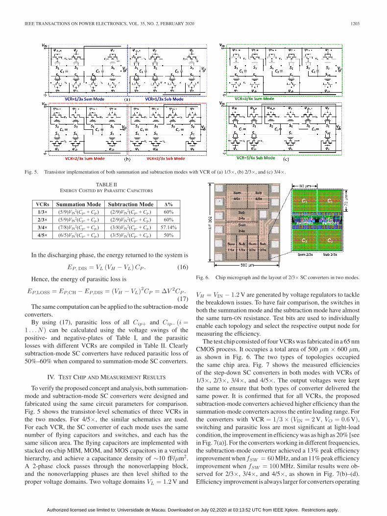
Fig. 5. Transistor implementation of both summation and subtraction modes with VCR of (a) 1/3×, (b) 2/3×, and (c) 3/4×.
TABLE IIENERGY COSTED BY PARASITIC CAPACITORS
In the discharging phase, the energy returned to the system is
EP, DIS = VL (VH − VL)CP . (16)
Hence, the energy of parasitic loss is
EP,LOSS = EP,CH − EP,DIS = (VH − VL)2CP = ΔV 2CP .
(17)The same computation can be applied to the subtraction-mode
converters.By using (17), parasitic loss of all Cip+ and Cip− (i =
1 . . . N) can be calculated using the voltage swings of thepositive- and negative-plates of Table I, and the parasiticlosses with different VCRs are compiled in Table II. Clearlysubtraction-mode SC converters have reduced parasitic loss of50%–60% when compared to summation-mode SC converters.
IV. TEST CHIP AND MEASUREMENT RESULTS
To verify the proposed concept and analysis, both summation-mode and subtraction-mode SC converters were designed andfabricated using the same circuit parameters for comparison.Fig. 5 shows the transistor-level schematics of three VCRs inthe two modes. For 4/5×, the similar schematics are used.For each VCR, the SC converter of each mode uses the samenumber of flying capacitors and switches, and each has thesame silicon area. The flying capacitors are implemented withstacked on-chip MIM, MOM, and MOS capacitors in a verticalhierarchy, and achieve a capacitance density of ∼10 fF/µm2.A 2-phase clock passes through the nonoverlapping block,and the nonoverlapping phases are then level shifted to theproper voltage domains. Two voltage domains VL = 1.2V and
Fig. 6. Chip micrograph and the layout of 2/3× SC converters in two modes.
VH = VIN − 1.2V are generated by voltage regulators to tacklethe breakdown issues. To have fair comparison, the switches inboth the summation mode and the subtraction mode have almostthe same turn-ON resistance. Test bits are used to individuallyenable each topology and select the respective output node formeasuring the efficiency.
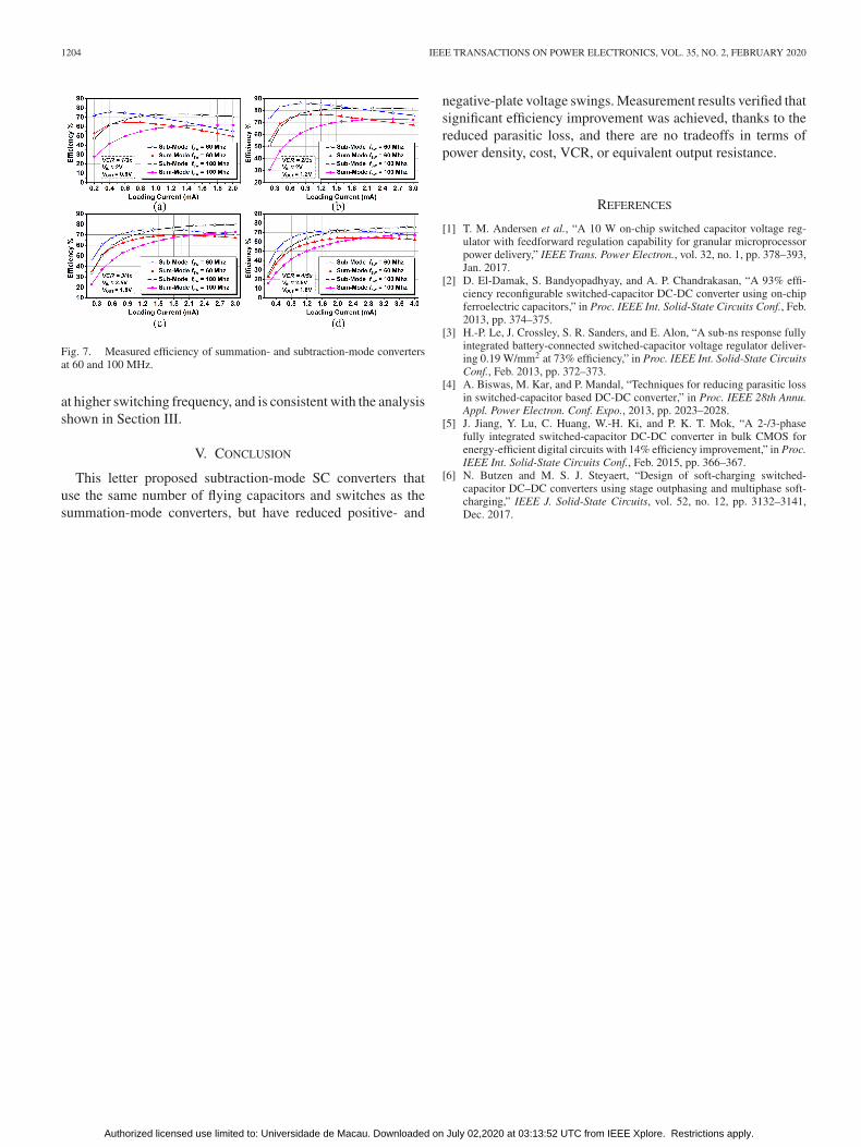
The test chip consisted of four VCRs was fabricated in a 65 nmCMOS process. It occupies a total area of 500 µm × 600 µm,as shown in Fig. 6. The two types of topologies occupiedthe same chip area. Fig. 7 shows the measured efficienciesof the step-down SC converters in both modes with VCRs of1/3×, 2/3×, 3/4×, and 4/5×. The output voltages were keptthe same to ensure that both types of converter delivered thesame power. It is confirmed that for all VCRs, the proposedsubtraction-mode converters achieved higher efficiency than thesummation-mode converters across the entire loading range. Forthe converters with VCR = 1/3× (VIN = 2V, VO = 0.6V),switching and parasitic loss are most significant at light-loadcondition, the improvement in efficiency was as high as 20% [seein Fig. 7(a)]. For the converters working in different frequencies,the subtraction-mode converter achieved a 13% peak efficiencyimprovement whenfSW = 60MHz, and an 11% peak efficiencyimprovement when fSW = 100MHz. Similar results were ob-served for 2/3×, 3/4×, and 4/5×, as shown in Fig. 7(b)–(d).Efficiency improvement is always larger for converters operating
Authorized licensed use limited to: Universidade de Macau. Downloaded on July 02,2020 at 03:13:52 UTC from IEEE Xplore. Restrictions apply.
1204 IEEE TRANSACTIONS ON POWER ELECTRONICS, VOL. 35, NO. 2, FEBRUARY 2020
Fig. 7. Measured efficiency of summation- and subtraction-mode convertersat 60 and 100 MHz.
at higher switching frequency, and is consistent with the analysisshown in Section III.
V. CONCLUSION
This letter proposed subtraction-mode SC converters thatuse the same number of flying capacitors and switches as thesummation-mode converters, but have reduced positive- and
negative-plate voltage swings. Measurement results verified thatsignificant efficiency improvement was achieved, thanks to thereduced parasitic loss, and there are no tradeoffs in terms ofpower density, cost, VCR, or equivalent output resistance.
REFERENCES
[1] T. M. Andersen et al., “A 10 W on-chip switched capacitor voltage reg-ulator with feedforward regulation capability for granular microprocessorpower delivery,” IEEE Trans. Power Electron., vol. 32, no. 1, pp. 378–393,Jan. 2017.
[2] D. El-Damak, S. Bandyopadhyay, and A. P. Chandrakasan, “A 93% effi-ciency reconfigurable switched-capacitor DC-DC converter using on-chipferroelectric capacitors,” in Proc. IEEE Int. Solid-State Circuits Conf., Feb.2013, pp. 374–375.
[3] H.-P. Le, J. Crossley, S. R. Sanders, and E. Alon, “A sub-ns response fullyintegrated battery-connected switched-capacitor voltage regulator deliver-ing 0.19 W/mm2 at 73% efficiency,” in Proc. IEEE Int. Solid-State CircuitsConf., Feb. 2013, pp. 372–373.
[4] A. Biswas, M. Kar, and P. Mandal, “Techniques for reducing parasitic lossin switched-capacitor based DC-DC converter,” in Proc. IEEE 28th Annu.Appl. Power Electron. Conf. Expo., 2013, pp. 2023–2028.
[5] J. Jiang, Y. Lu, C. Huang, W.-H. Ki, and P. K. T. Mok, “A 2-/3-phasefully integrated switched-capacitor DC-DC converter in bulk CMOS forenergy-efficient digital circuits with 14% efficiency improvement,” in Proc.IEEE Int. Solid-State Circuits Conf., Feb. 2015, pp. 366–367.
[6] N. Butzen and M. S. J. Steyaert, “Design of soft-charging switched-capacitor DC–DC converters using stage outphasing and multiphase soft-charging,” IEEE J. Solid-State Circuits, vol. 52, no. 12, pp. 3132–3141,Dec. 2017.
Authorized licensed use limited to: Universidade de Macau. Downloaded on July 02,2020 at 03:13:52 UTC from IEEE Xplore. Restrictions apply.