Embed Size (px)
Citation preview
92
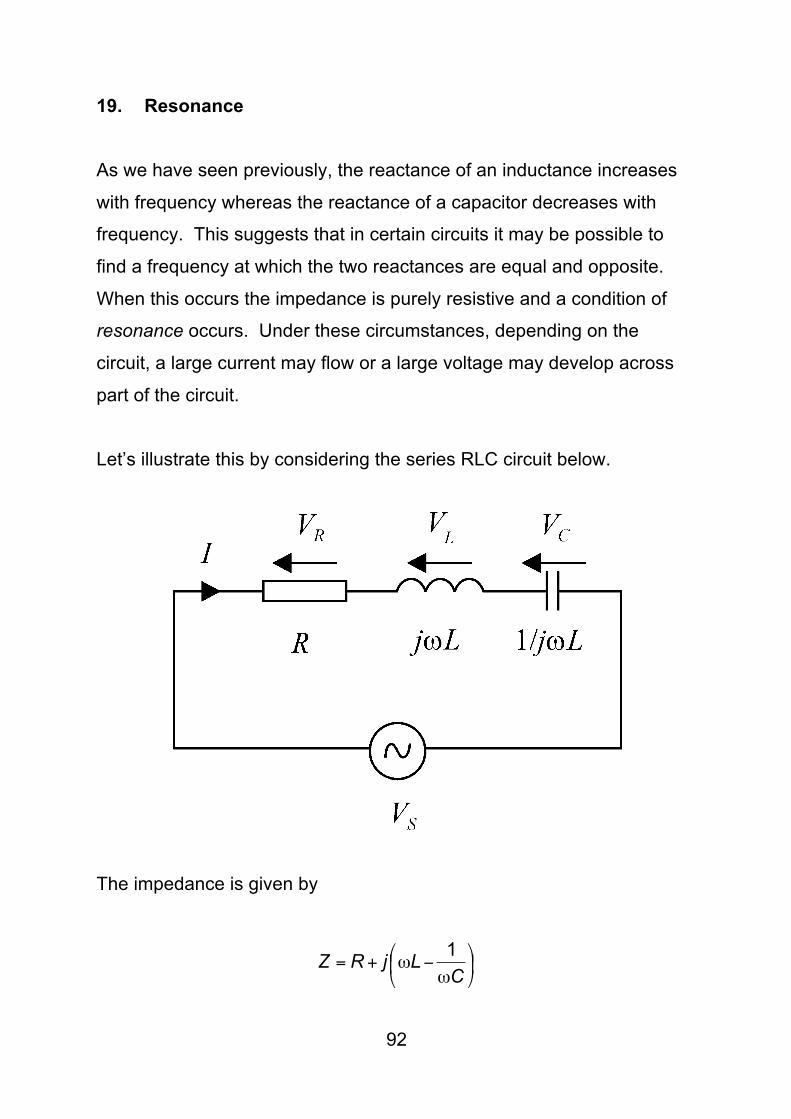
19. Resonance As we have seen previously, the reactance of an inductance increases
with frequency whereas the reactance of a capacitor decreases with
frequency. This suggests that in certain circuits it may be possible to
find a frequency at which the two reactances are equal and opposite.
When this occurs the impedance is purely resistive and a condition of
resonance occurs. Under these circumstances, depending on the
circuit, a large current may flow or a large voltage may develop across
part of the circuit.
Let’s illustrate this by considering the series RLC circuit below.
The impedance is given by
⎟⎠
⎞⎜⎝
⎛ω
−ω+=C
LjRZ 1
Circuit Analysis II WRM MT11
93
Clearly Z is a minimum when ωL = 1/ωC when it has the real value Z =
R. The frequency at which this occurs is called the “resonant”
frequency, ω0, which is given by
LC1
0 =ω
The voltages and current are related by
ICjLjR
VVVV CLRS
⎟⎠
⎞⎜⎝
⎛ω
−ω+=
++=
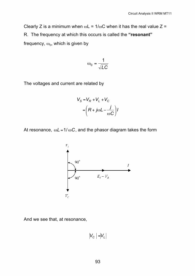
At resonance, CL ω=ω /1 , and the phasor diagram takes the form
And we see that, at resonance,
LC VV =
94
and that the current, I¸ and the voltage, VS, are in phase and are related
by
IRVS=
As the frequency changes from its values at resonance the current, I,
falls from the maximum value of VS/R. At resonance the impedance
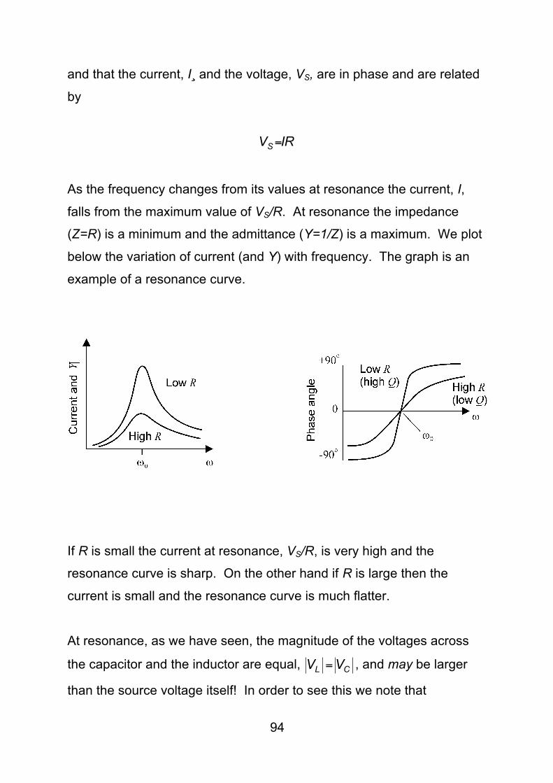
(Z=R) is a minimum and the admittance (Y=1/Z) is a maximum. We plot
below the variation of current (and Y) with frequency. The graph is an
example of a resonance curve.
If R is small the current at resonance, VS/R, is very high and the
resonance curve is sharp. On the other hand if R is large then the
current is small and the resonance curve is much flatter.
At resonance, as we have seen, the magnitude of the voltages across
the capacitor and the inductor are equal, CL VV = , and may be larger
than the source voltage itself! In order to see this we note that
Circuit Analysis II WRM MT11
95
LIVL 0ω= , CIVC 0/ω= and IRVS = . Thus
CRRL
VV
VV
S
C
S
L
0
0 1ω
=ω
==
which can be made very high by making R small. The ratio, S
L
VV
or S
C
VV
represents the ‘voltage magnification’ and is known as the “quality factor”, Q, of the circuit. Thus
Q =magnitude of voltage across L or C at resonance
magnitude of voltage across whole circuit
=ω0LR
=1
ω0CR
A high Q also results in a sharp response curve. This suggests that the
circuit acts as a narrow band filter since it only passes significant current
near the resonant frequency, 0ω=ω .
[In the lab, when you build a tuned circuit for a radio receiver, the
inductor will always come with some resistance and this will limit the Q
that is achievable. We sometimes therefore refer to Q =ω0LR as the “Q
of the coil”.]
96
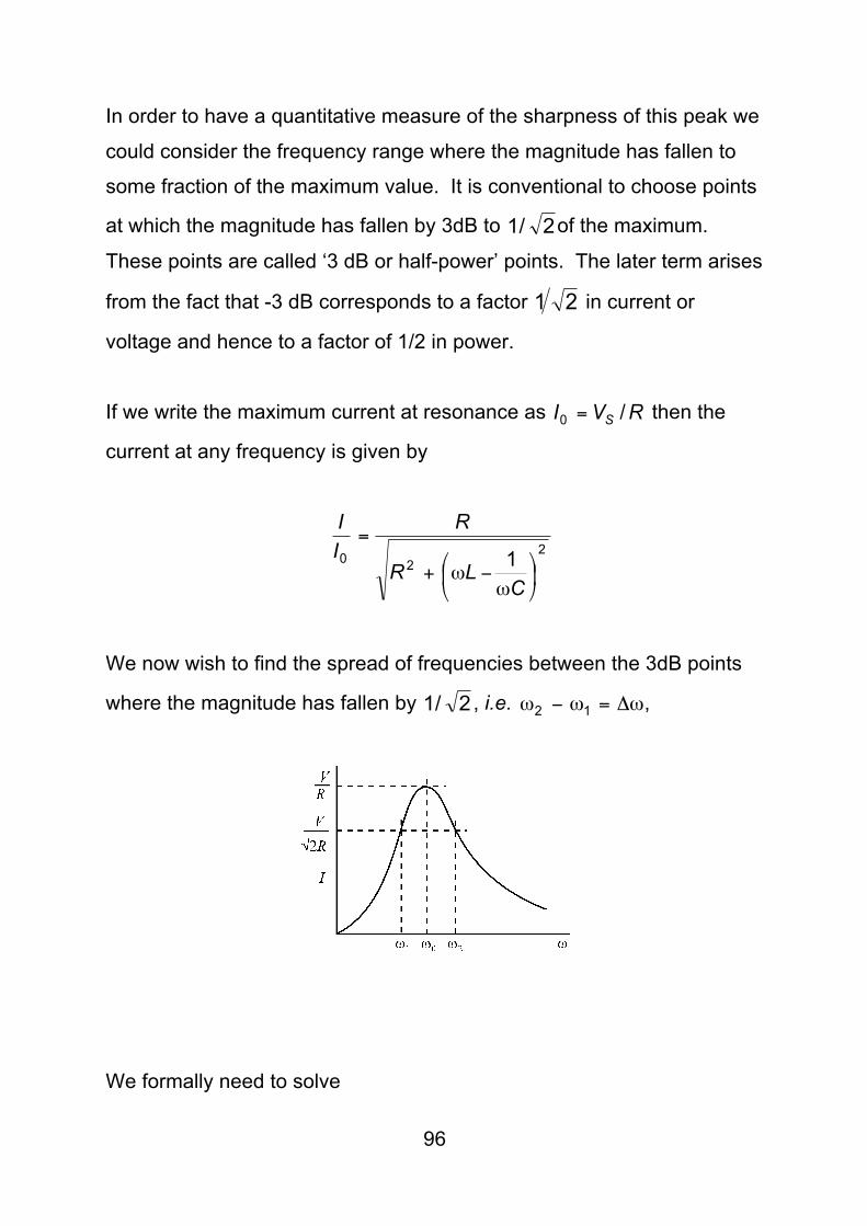
In order to have a quantitative measure of the sharpness of this peak we
could consider the frequency range where the magnitude has fallen to
some fraction of the maximum value. It is conventional to choose points
at which the magnitude has fallen by 3dB to 2/1 of the maximum.
These points are called ‘3 dB or half-power’ points. The later term arises
from the fact that -3 dB corresponds to a factor 21 in current or
voltage and hence to a factor of 1/2 in power.
If we write the maximum current at resonance as RVI S /0 = then the
current at any frequency is given by
220 1
⎟⎠
⎞⎜⎝
⎛ω
−ω+
=
CLR
RII
We now wish to find the spread of frequencies between the 3dB points
where the magnitude has fallen by 2/1 , i.e. ωΔ=ω−ω 12 ,
We formally need to solve
Circuit Analysis II WRM MT11
97
21
1 22
=
⎟⎠
⎞⎜⎝
⎛ω
−ω+C
LR
R
or, equivalently,
RC
L ±=⎟⎠
⎞⎜⎝
⎛ω
−ω1
We take the negative sign to correspond to the lower frequency, ω1.
Solving the resulting quadratic gives
LCLR
LR 1
22
2
1 +⎟⎠
⎞⎜⎝
⎛+−=ω
where the positive square root has been taken in order to give a positive
ω1.
Similarly the higher frequency, ω2, is obtained by taking the +R sign. In
this case we obtain
LCLR
LR 1
22
2
2 +⎟⎠
⎞⎜⎝
⎛+=ω
The frequency difference between the 3dB points is therefore
98
Δω = ω2 − ω1 =RL
which together with our previous definition of RL
Q 0ω= permits us to
write
ωΔ
ω=
ω= 00
RL
Q
and so the higher the Q the narrower the bandwidth, Δω, and the
sharper the resonance peak.
We note that although we first defined Q in terms of the ‘voltage
magnification’ we could just as easily used ωΔ
ω= 0Q as an alternative
definition.
We also note that the resonant frequency 0ω is not positioned midway
between the two 3dB frequencies 2ω and 1ω . It is, in fact, the
geometrical mean of the two as can be seen by multiplying the
equations for 2ω and 1ω together
210 ωω=ω
and hence, on a Bode plot where a logarithmic frequency scale is used,
2ω and 1ω will be symmetrical about 0ω .
Circuit Analysis II WRM MT11
99
Let us finally return to the circuit and consider the voltage across the
capacitor, VC. It is easy to write
⎭⎬⎫
⎩⎨⎧
⎟⎠
⎞⎜⎝
⎛ω
−ω+ω
=ω
=
CLjRCj
VCjIV S
C 1
and hence
( ) LCjCRjVV
S
C21
1ω+ω+
=
Now, if we recall that LC=ω0 and CRRLQ 00 /1/ ω=ω= then we
may write
VCVS
=1
1+ j 1Q
ωω0
!
"##
$
%&&+ j ω
ω0
!
"##
$
%&&
2
We see that the denominator here is of the standard form we discussed
earlier where the Q factor is evidently related to the damping factor, ζ,
via
ς=21Q
100
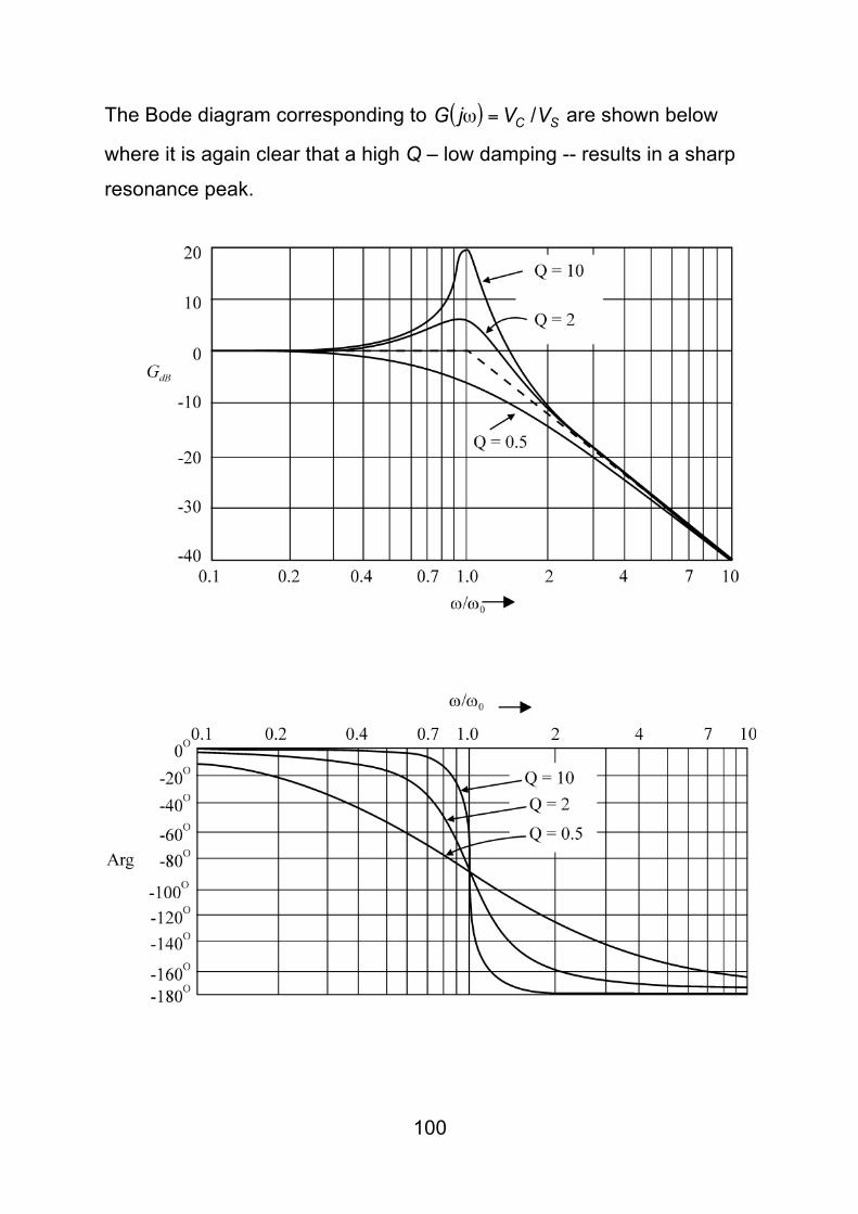
The Bode diagram corresponding to ( ) SC VVjG /=ω are shown below
where it is again clear that a high Q – low damping -- results in a sharp
resonance peak.
Circuit Analysis II WRM MT11
101
[i.e. Exactly this frequency response function is plotted in HLT page
168.]
Example
In a particular series RLC circuit, R = 10 Ω , L = 1 mH and C = 0.1 µF
and the source VS = 2.0 V rms.
The resonant frequency, ω0, is given by
rad/secLC
50 101
==ω
which may be expressed as kHzf 9.152/00 =πω= . The Q of the
circuit is
100 =ω
=RL
Q
and hence the bandwidth, Q/0ω=ωΔ , or kHz.Qff 59.1/00 ==Δ
The current at resonance is
ARV
I S 2.00 ==
and the magnitude of the voltage across either the capacitor or the
inductor at resonance is
102
VQVV S 20==
General remark on Q
We have defined Q in a way that is convenient for our ‘electrical’
purposes. However, since all resonant systems – mechanical and
electrical – have a common basis in energy, it is also possible to show
that
cycle per dissipated energystored energyQ π= 2
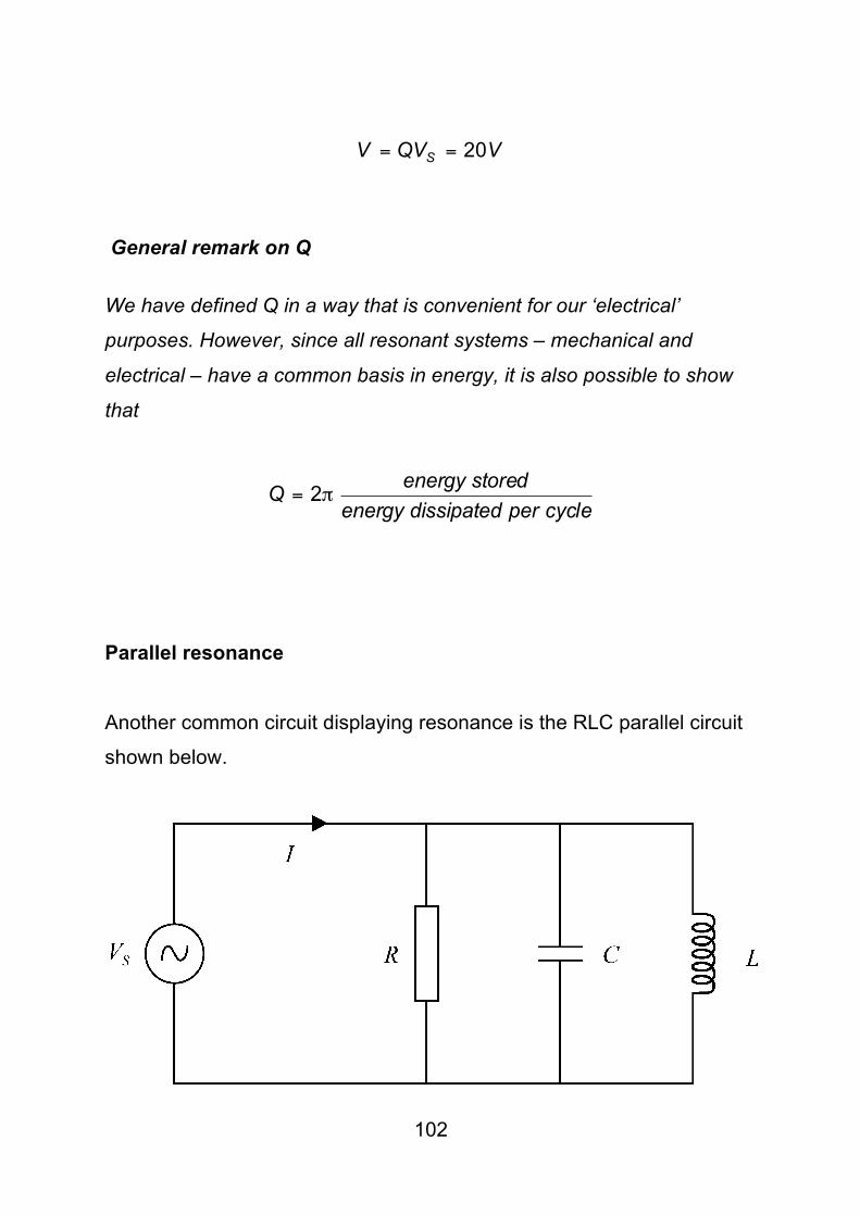
Parallel resonance
Another common circuit displaying resonance is the RLC parallel circuit
shown below.
Circuit Analysis II WRM MT11
103
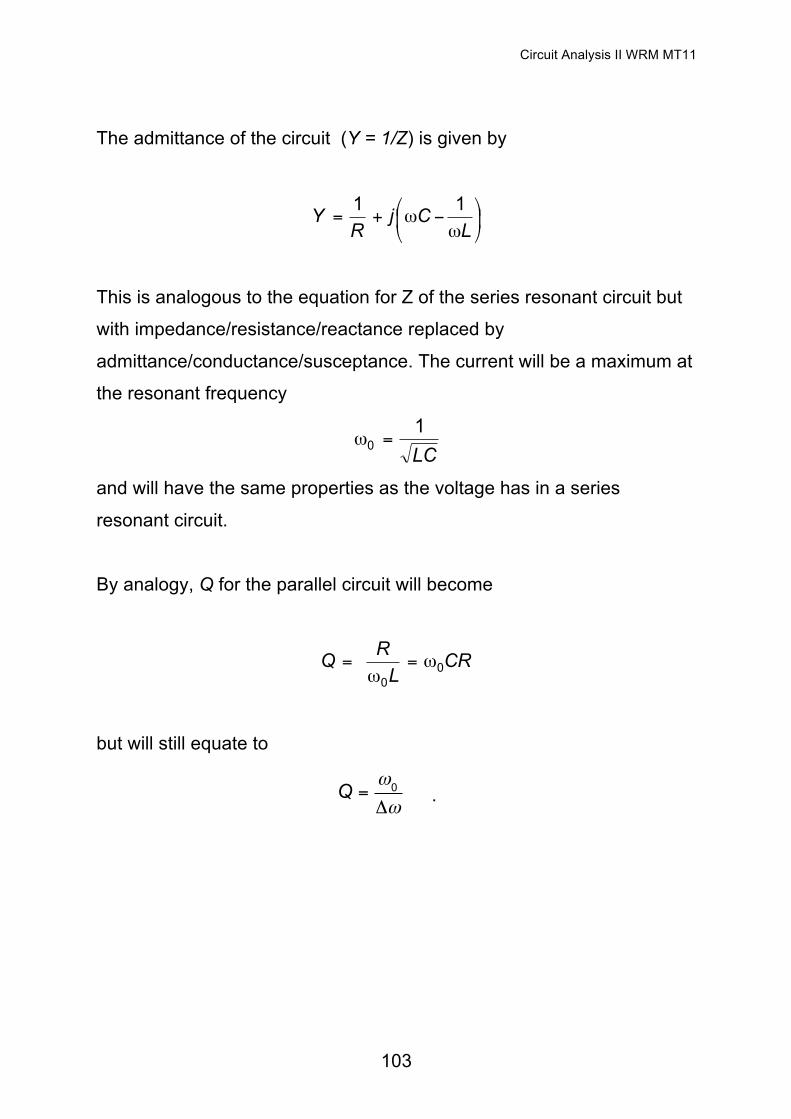
The admittance of the circuit (Y = 1/Z) is given by
⎟⎠
⎞⎜⎝
⎛ω
−ω+=L
CjR
Y 11
This is analogous to the equation for Z of the series resonant circuit but
with impedance/resistance/reactance replaced by
admittance/conductance/susceptance. The current will be a maximum at
the resonant frequency
LC1
0 =ω
and will have the same properties as the voltage has in a series
resonant circuit.
By analogy, Q for the parallel circuit will become
CRLRQ 00
ω=ω
=
but will still equate to
Q =ω0
Δω .
104
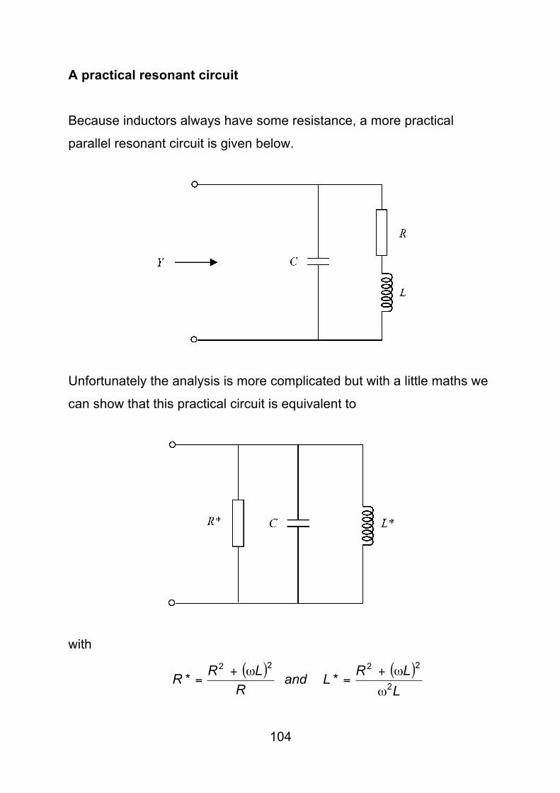
A practical resonant circuit
Because inductors always have some resistance, a more practical
parallel resonant circuit is given below.
Unfortunately the analysis is more complicated but with a little maths we
can show that this practical circuit is equivalent to
with
( ) ( )LLR*Land
RLRR 2
2222
*ω
ω+=
ω+=

Circuit Analysis II WRM MT11
105
For high enough Q, we can use the simple approximations in HLT (page
167).
106
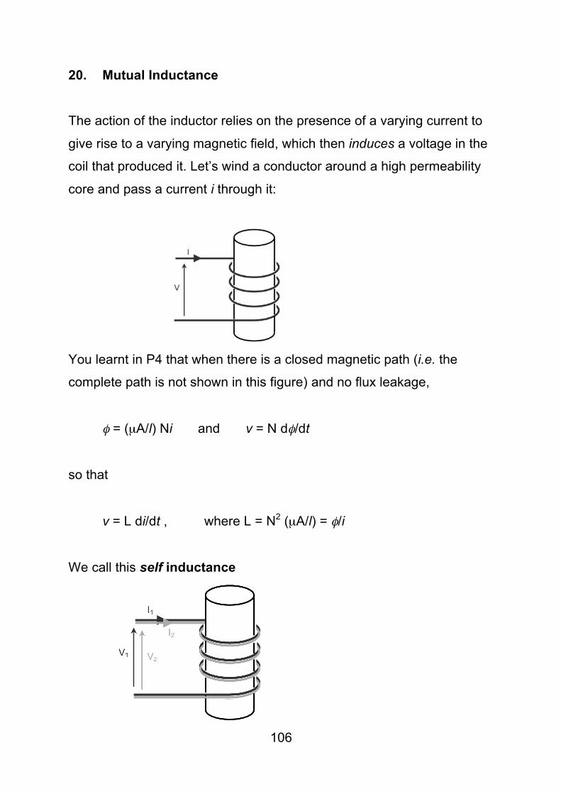
20. Mutual Inductance
The action of the inductor relies on the presence of a varying current to
give rise to a varying magnetic field, which then induces a voltage in the
coil that produced it. Let’s wind a conductor around a high permeability
core and pass a current i through it:
You learnt in P4 that when there is a closed magnetic path (i.e. the
complete path is not shown in this figure) and no flux leakage,
φ = (µA/l) Ni and v = N dφ/dt
so that
v = L di/dt , where L = N2 (µA/l) = φ/i
We call this self inductance
Circuit Analysis II WRM MT11
107
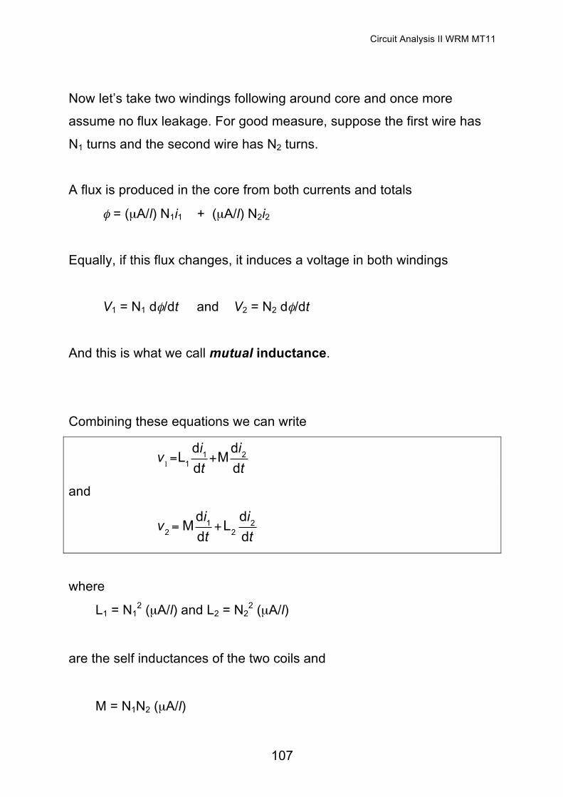
Now let’s take two windings following around core and once more
assume no flux leakage. For good measure, suppose the first wire has
N1 turns and the second wire has N2 turns.
A flux is produced in the core from both currents and totals
φ = (µA/l) N1i1 + (µA/l) N2i2
Equally, if this flux changes, it induces a voltage in both windings
V1 = N1 dφ/dt and V2 = N2 dφ/dt
And this is what we call mutual inductance.
Combining these equations we can write
v1=L1
di1dt+M
di2dt
and
v2 =M
di1dt
+L2di2dt
where
L1 = N12 (µA/l) and L2 = N2
2 (µA/l)
are the self inductances of the two coils and
M = N1N2 (µA/l)
108
is the mutual inductance between the two coils.
Perfect Coupling
Note that in this ideal world of perfect flux coupling, M = √(L1L2).
Magnetic Coupling Coefficient
In practice we always get some flux leakage, i.e. not all the flux stays in
the core and therefore not all the flux links all the coils. We should
therefore expect that
L1 < N12 (µA/l) and L2 < N2
2 (µA/l)
and
M < √(L1L2)
We can then write
M = k . √(L1L2)
where k (0 < k < 1) is known as the “coupling coefficient”.
Circuit Analysis II WRM MT11
109
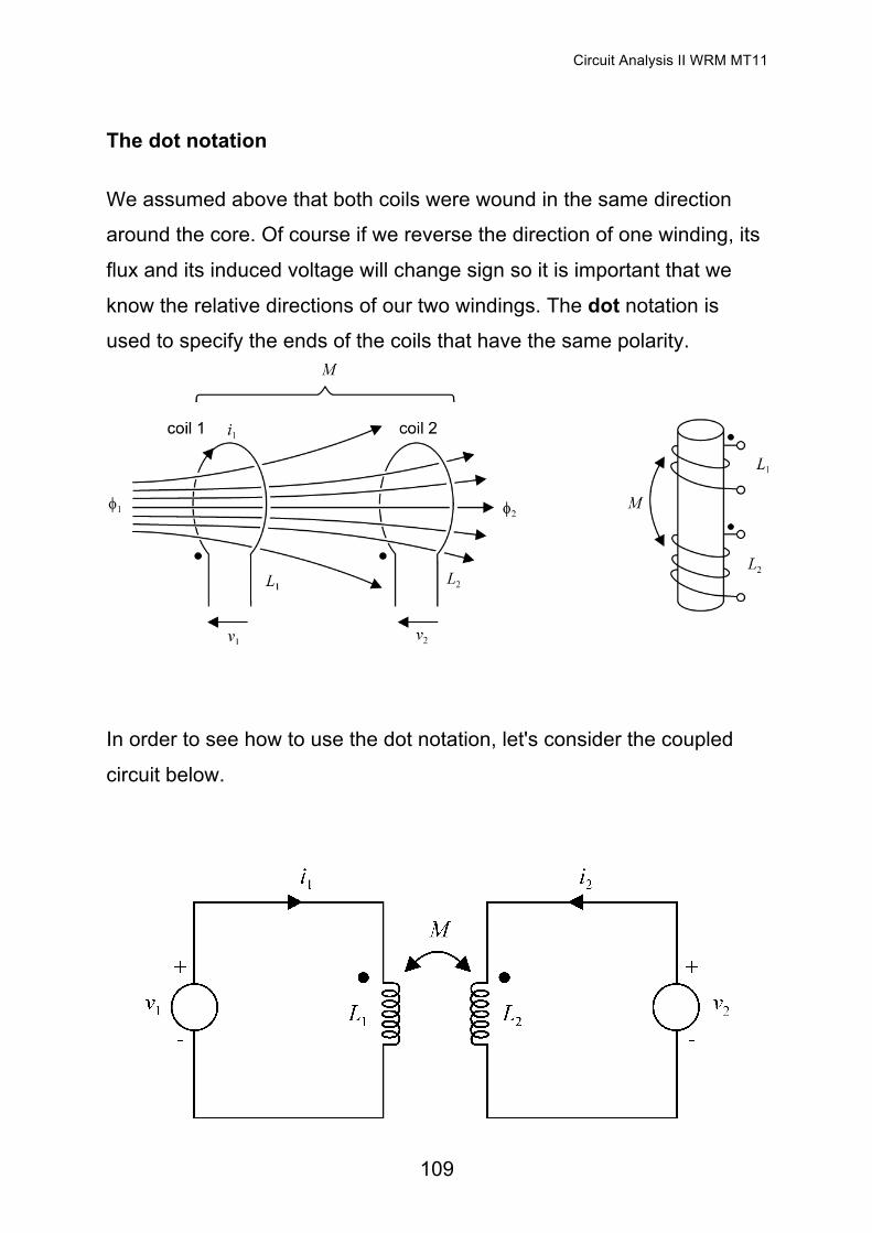
The dot notation
We assumed above that both coils were wound in the same direction
around the core. Of course if we reverse the direction of one winding, its
flux and its induced voltage will change sign so it is important that we
know the relative directions of our two windings. The dot notation is
used to specify the ends of the coils that have the same polarity.
In order to see how to use the dot notation, let's consider the coupled
circuit below.
110
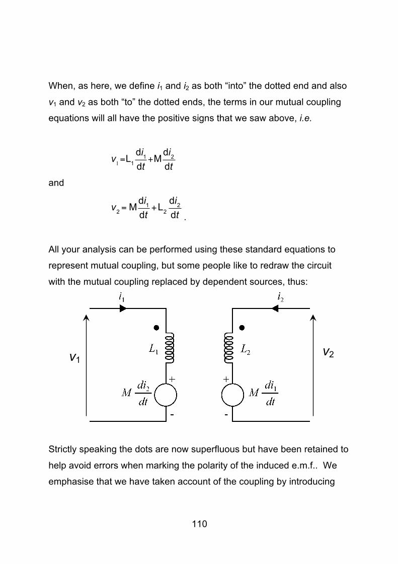
When, as here, we define i1 and i2 as both “into” the dotted end and also
v1 and v2 as both “to” the dotted ends, the terms in our mutual coupling
equations will all have the positive signs that we saw above, i.e.
v1=L1
di1dt+M
di2dt
and
v2 =M
di1dt
+L2di2dt .
All your analysis can be performed using these standard equations to
represent mutual coupling, but some people like to redraw the circuit
with the mutual coupling replaced by dependent sources, thus:
Strictly speaking the dots are now superfluous but have been retained to
help avoid errors when marking the polarity of the induced e.m.f.. We
emphasise that we have taken account of the coupling by introducing
v1 v2
Circuit Analysis II WRM MT11
111
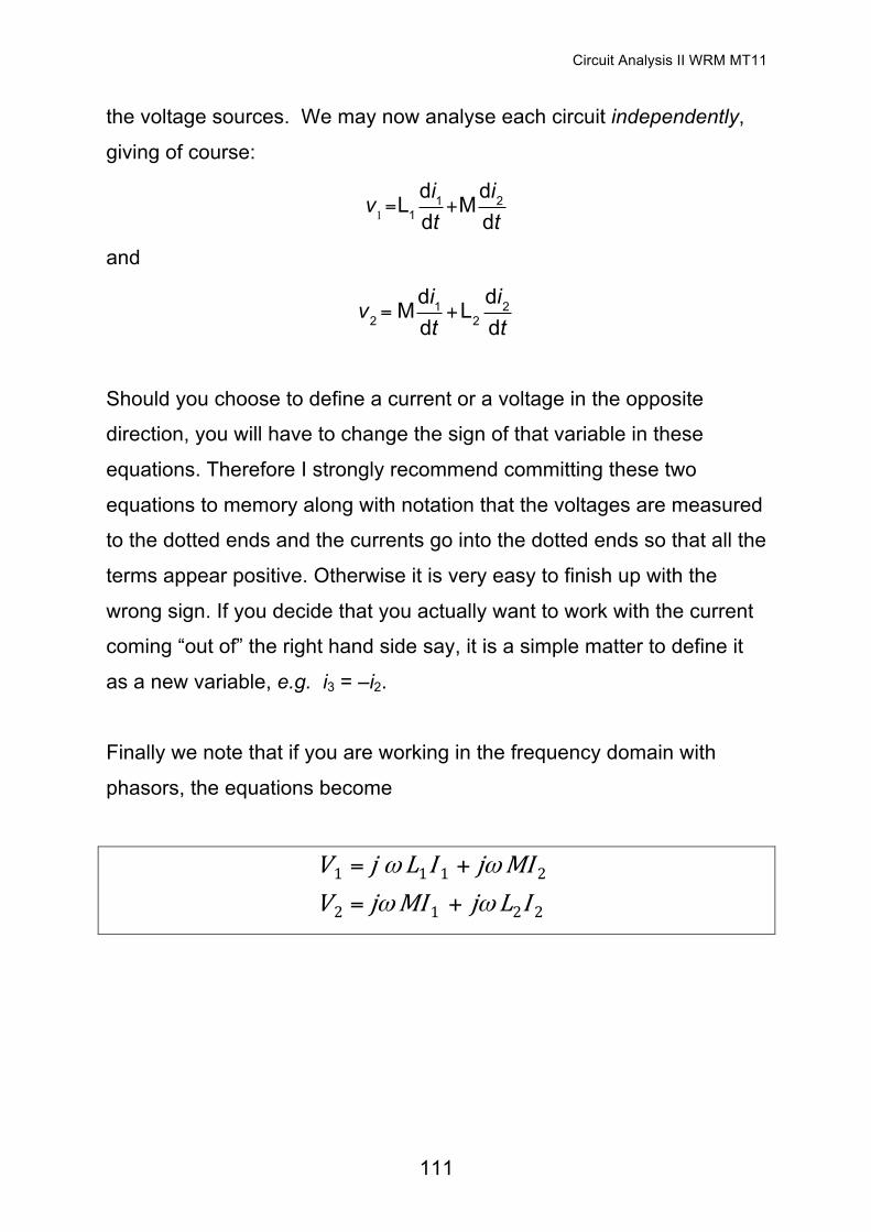
the voltage sources. We may now analyse each circuit independently,
giving of course:
v1=L1di1dt+M
di2dt
and
v2 =Mdi1dt
+L2di2dt
Should you choose to define a current or a voltage in the opposite
direction, you will have to change the sign of that variable in these
equations. Therefore I strongly recommend committing these two
equations to memory along with notation that the voltages are measured
to the dotted ends and the currents go into the dotted ends so that all the
terms appear positive. Otherwise it is very easy to finish up with the
wrong sign. If you decide that you actually want to work with the current
coming “out of” the right hand side say, it is a simple matter to define it
as a new variable, e.g. i3 = –i2.
Finally we note that if you are working in the frequency domain with
phasors, the equations become
2212
2111
ILjMIjVMIjILjV
ωω
ωω
+=
+=
112
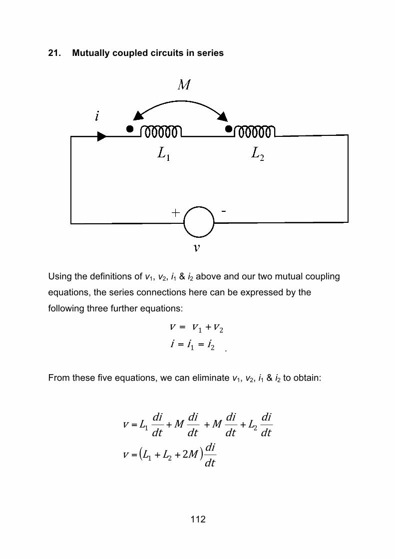
21. Mutually coupled circuits in series
Using the definitions of v1, v2, i1 & i2 above and our two mutual coupling
equations, the series connections here can be expressed by the
following three further equations:
21
21
iiiv vv
==
+=
.
From these five equations, we can eliminate v1, v2, i1 & i2 to obtain:
( )dtdiMLLv
dtdiL
dtdiM
dtdiM
dtdiLv
221
21
++=
+++=
Circuit Analysis II WRM MT11
113
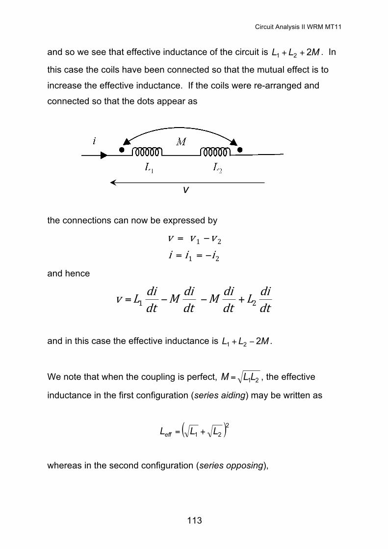
and so we see that effective inductance of the circuit is MLL 221 ++ . In
this case the coils have been connected so that the mutual effect is to
increase the effective inductance. If the coils were re-arranged and
connected so that the dots appear as
the connections can now be expressed by
21
21
iiiv vv−==
−=
and hence
dtdiL
dtdiM
dtdiM
dtdiLv 21 +−−=
and in this case the effective inductance is MLL 221 −+ .
We note that when the coupling is perfect, 21LLM = , the effective
inductance in the first configuration (series aiding) may be written as
( )221 LLLeff +=
whereas in the second configuration (series opposing),
v
114
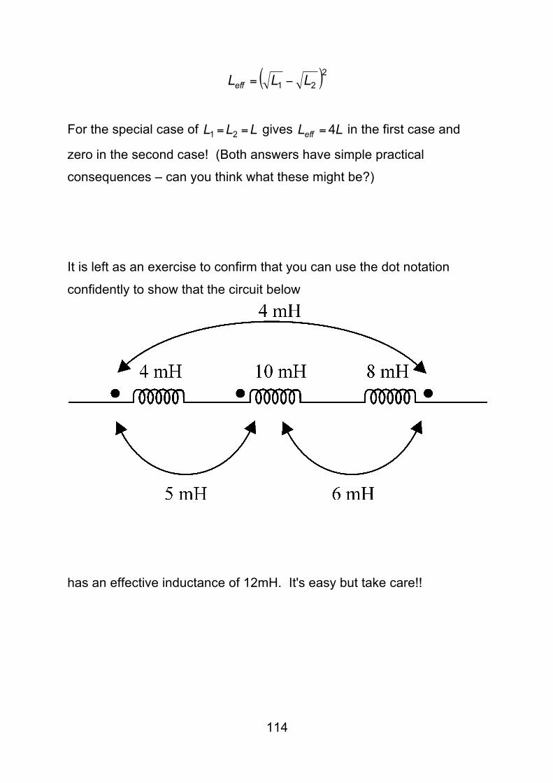
( )221 LLLeff −=
For the special case of LLL == 21 gives LLeff 4= in the first case and
zero in the second case! (Both answers have simple practical
consequences – can you think what these might be?)
It is left as an exercise to confirm that you can use the dot notation
confidently to show that the circuit below
has an effective inductance of 12mH. It's easy but take care!!
Circuit Analysis II WRM MT11
115
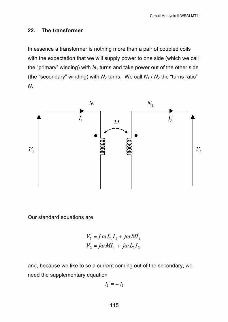
22. The transformer
In essence a transformer is nothing more than a pair of coupled coils
with the expectation that we will supply power to one side (which we call
the “primary” winding) with N1 turns and take power out of the other side
(the “secondary” winding) with N2 turns. We call N1 / N2 the “turns ratio”
N.
Our standard equations are
and, because we like to se a current coming out of the secondary, we
need the supplementary equation
I2’ = – I2
2212
2111
ILjMIjVMIjILjV
ωω
ωω
+=
+=
I2’
116
In an “ideal transformer” with no flux leakage, 221
2212 NNNLL == and
21LLM = so we can write the equations for V1 and V2 in terms of L1
alone as:
V1 = jω L1 I1 + jω NL1 I2
V2 = jω NL1 I1 + jω N2L1 I2
From which we deduce that
111
22 NVV
NNV ==
Thus we can use a transformer to “transform” power from one voltage to
another by selecting an appropriate turns ratio. For example, to "step
down" the mains 230V & 50 Hz to something more useful for electronic
circuits, say 12V. Alternatively a transformer can be used to "step up"
voltages from a generator for transmission over large distances.
Since our transformer does not dissipate any power, it is tempting to
think that V.I is the same at the primary and secondary and that when
the voltage is 'transformed' by a factor N the current will be 'transformed'
by the inverse factor 1/N. However, this would to be to ignore the phase
shift in the output current. By eliminating I2 we obtain
''2
1
12
11
11 NI
LjVI
LM
LjVI +=+=
ωω
Circuit Analysis II WRM MT11
117
from which we see that the ideal current relationship will be approached
by making 1L large. That’s why we like lots of windings!
We conclude this section by working out the input impedance of an
ideal transformer when it is connected to a load ZL. When the load is in
place we have LZIV '22 = and the equations become
'2111 IMjILjV ωω −=
''2212 ILjMIjZI L ωω −=
The input impedance is defined as 11 IVZin = which, after a little algebra
gives
( )L
Lin ZLj
LLMZLjIVZ
+ω
−ω+ω==
2
2122
1
1
1
For our ideal ideal transformer with 212 LLM = when the inductances are
large enough we approximate
Lin ZLLZ2
1=
or
118
2NZZ L
in =
Therefore, as well as being useful for transforming currents and voltages
transformers are also used to transform impedances. In this case the
source "sees" an effective load of 2NZL . This can be useful when
coupling signals to very low impedance loads. Indeed if you elect to use
earphones in the radio you will build in the DBT exercise you may have
occasion to use a transformer in this way.
Circuit Analysis II WRM MT11
119
23. Transient response
In our previous analysis of circuits we were concerned with the 'steady
state' solutions for current and voltage, which occur long after the source
or sources have been connected to the circuit. Since the current/voltage
relationships for capacitors and inductors involve time derivatives they
clearly do not respond instantly to abrupt changes in current and
voltage. It takes time for the effects of an abrupt change to die away
and for the final steady state conditions to be reached.
When we began discussing AC circuit theory we set up the governing
differential equation and proceeded to solve it using standard
mathematical techniques. The full solution consisted of two terms. The
first, the complementary function, corresponded to the transient
response which eventually decayed away whereas the second, the
particular integral, led to the final steady state response. In the RL
circuit you built in the laboratory the steady state was achieved in a
matter of milliseconds and so the transient component was not evident
in the measurements you took. However, a millisecond, or even a
microsecond, can be a long time in electrical engineering and hence
transients deserve our attention.
We will now discuss in more detail the effects of abruptly connecting or
disconnecting sources to electrical circuits. Previously we have only
dealt with sinusoidally varying sources but we will now remove this
restriction. In order to introduce the topic logically we will begin by
considering first order systems; so called because they contain only
resistive and one reactive element and lead to first order differential
equations before moving on to second order systems containing
120
resistors and two reactive elements. At first we will solve the differential
equations using standard 'classical' mathematics before introducing a
powerful (and simple) technique based on the Laplace transform.
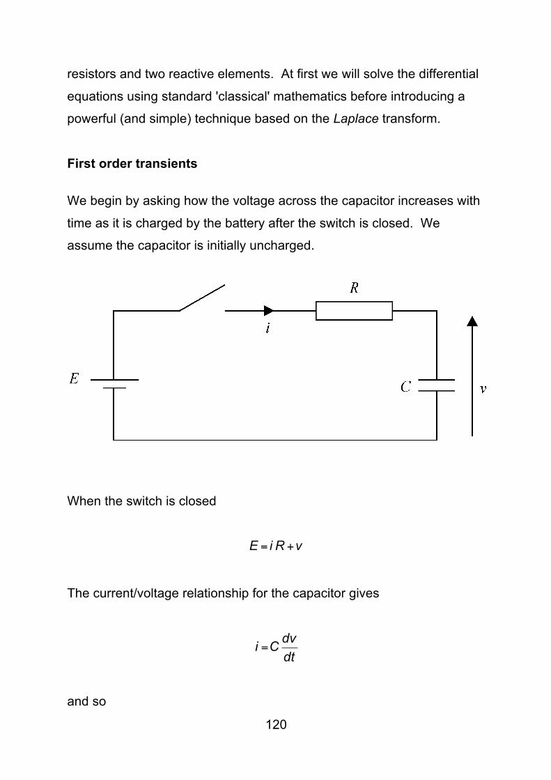
First order transients
We begin by asking how the voltage across the capacitor increases with
time as it is charged by the battery after the switch is closed. We
assume the capacitor is initially uncharged.
When the switch is closed
vRiE +=
The current/voltage relationship for the capacitor gives
dtdvCi =
and so
Circuit Analysis II WRM MT11
121
vdtdvRCE +=
or
RCE
RCv
dtdv
=+
where, evidently, as we have seen before, the product RC must have
the dimensions of time. Thus we set RC=T and we formally now need to
solve
TE
Tv
dtdv
=+
We begin by considering the complementary function as the solution of
0=+Tv
dtdv . A suitable candidate is ( )mtAexp which leads to an auxiliary
equation
Tm
Tm 1;01
−==+
and hence the complementary function is TtA −exp . The particular
integral is determined by the specific forcing function applied. In this
case it is constant (a battery) and hence a suitable particular integral is
Ev = . The full solution is provided by
122
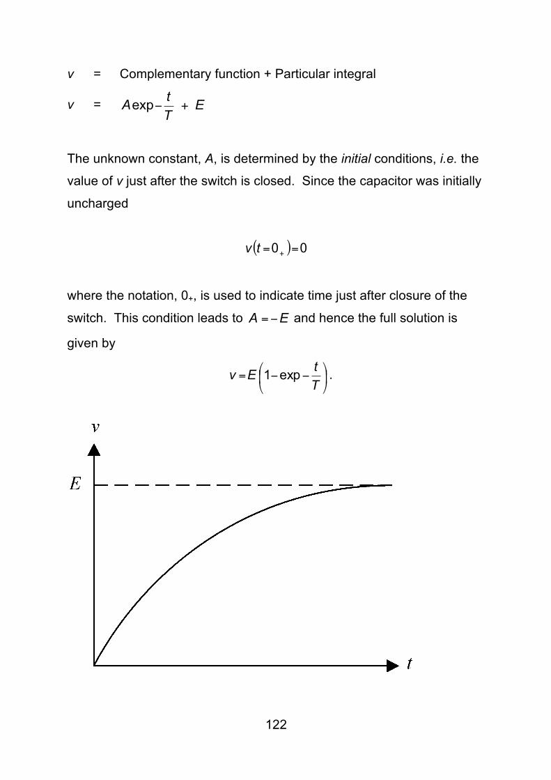
v = Complementary function + Particular integral
v = ETtA +−exp
The unknown constant, A, is determined by the initial conditions, i.e. the
value of v just after the switch is closed. Since the capacitor was initially
uncharged
( ) 00 == +tv
where the notation, 0+, is used to indicate time just after closure of the
switch. This condition leads to EA −= and hence the full solution is
given by
⎟⎠
⎞⎜⎝
⎛ −−=TtEv exp1 .
Circuit Analysis II WRM MT11
123
The factor RCT = is known as the time constant and indicates how
quickly the capacitor charges.
We can now make some general remarks about the form of this solution
(i) The complementary function, TReA − , determines the transient
response which decays away at a rate determined by the time
constant, T. The unknown constant, A is determined by the initial
conditions.
(ii) The particular integral leads to the final steady state solution. As
such it is determined by the specific forcing function – constant in
this case, (sinusoidal in our previous discussion) – and not by the
initial conditions. It is, of course, independent of the initial
conditions.
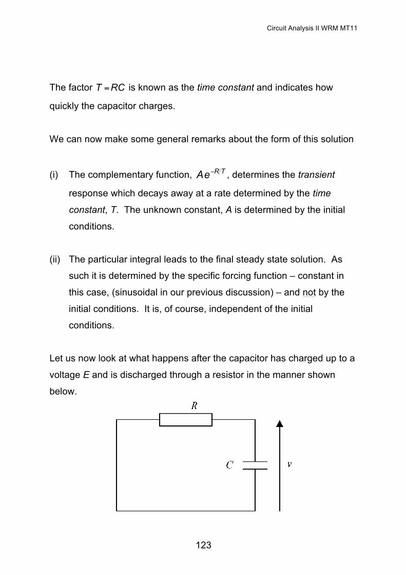
Let us now look at what happens after the capacitor has charged up to a
voltage E and is discharged through a resistor in the manner shown
below.
124
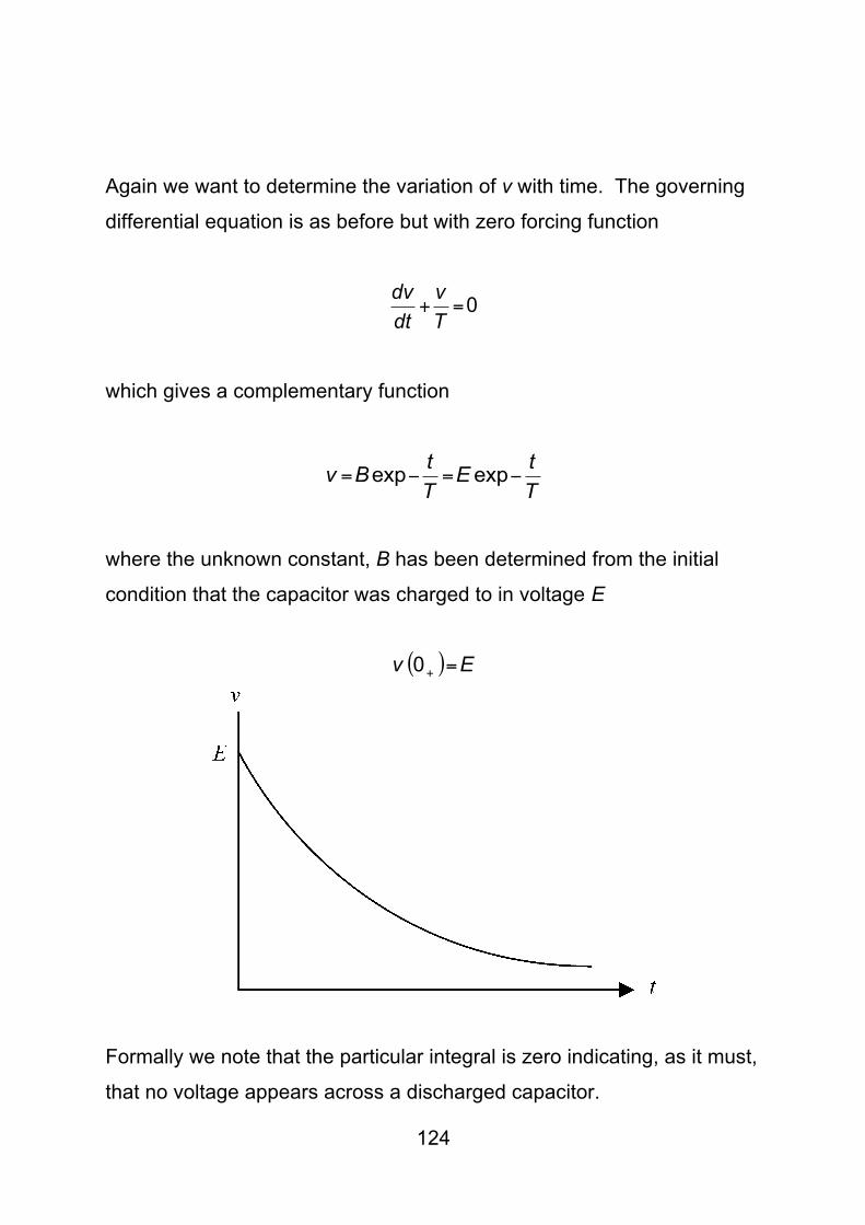
Again we want to determine the variation of v with time. The governing
differential equation is as before but with zero forcing function
0=+Tv
dtdv
which gives a complementary function
TtE
TtBv −=−= expexp
where the unknown constant, B has been determined from the initial
condition that the capacitor was charged to in voltage E
( ) Ev =+0
Formally we note that the particular integral is zero indicating, as it must,
that no voltage appears across a discharged capacitor.
Circuit Analysis II WRM MT11
125
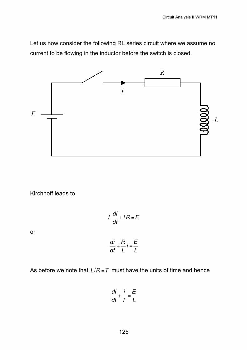
Let us now consider the following RL series circuit where we assume no
current to be flowing in the inductor before the switch is closed.
Kirchhoff leads to
ERidtdiL =+
or
LEi
LR
dtdi
=+
As before we note that TRL = must have the units of time and hence
LE
Ti
dtdi
=+
126
which is mathematically, formally, equivalent to the differential equation
we previously encountered. The complementary function is again given
by
TtA −exp
with time constant RLT = and unknown constant A. The particular
integral is
RE
LTE=
and hence the full solution
RE
TtAi +−= exp
The initial condition, ( ) 00 =+i leads to REA −= and hence
⎭⎬⎫
⎩⎨⎧ −−=
Tt
REi exp1
which again, has the standard form with a time constant, RLT = .
It is left as an exercise to show that if we discharge the inductor through
the resistor that the current decays as Tt
REi −= exp .
Circuit Analysis II WRM MT11
127
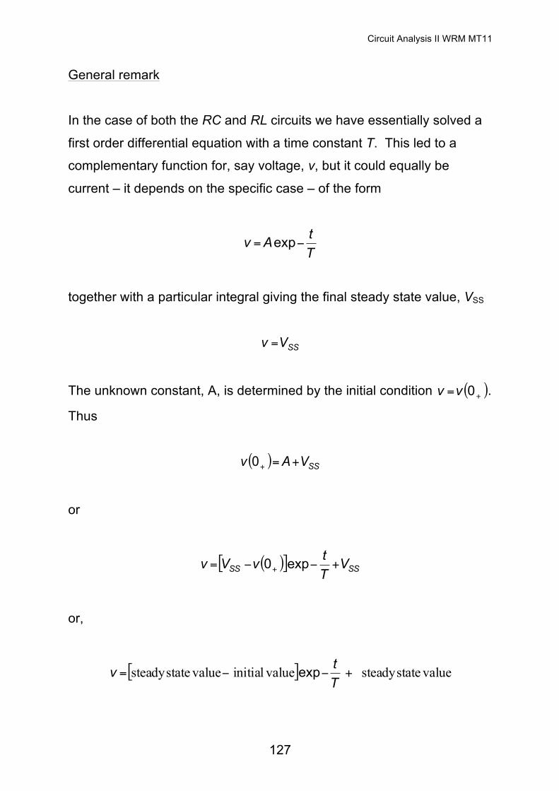
General remark
In the case of both the RC and RL circuits we have essentially solved a
first order differential equation with a time constant T. This led to a
complementary function for, say voltage, v, but it could equally be
current – it depends on the specific case – of the form
TtAv −= exp
together with a particular integral giving the final steady state value, VSS
SSVv =
The unknown constant, A, is determined by the initial condition ( )+= 0vv .
Thus
( ) SSVAv +=+0
or
( )[ ] SSSS VTtvVv +−−= + exp0
or,
[ ] valuestatesteadyvalueinitialvaluestatesteady +−−=Ttv exp
128
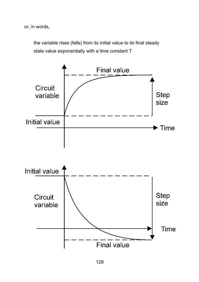
or, in words,
the variable rises (falls) from its initial value to its final steady
state value exponentially with a time constant T
Circuit Analysis II WRM MT11
129
This observation permits us to sketch the transient response of many
simple circuits by inspection.
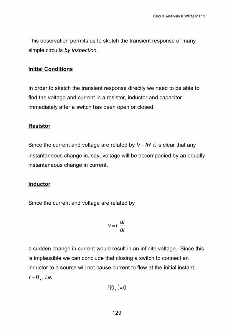
Initial Conditions
In order to sketch the transient response directly we need to be able to
find the voltage and current in a resistor, inductor and capacitor
immediately after a switch has been open or closed.
Resistor
Since the current and voltage are related by IRV = it is clear that any
instantaneous change in, say, voltage will be accompanied by an equally
instantaneous change in current.
Inductor
Since the current and voltage are related by
dtdiLv =
a sudden change in current would result in an infinite voltage. Since this
is implausible we can conclude that closing a switch to connect an
inductor to a source will not cause current to flow at the initial instant,
+= 0t , i.e.
( ) 00 =+i
130
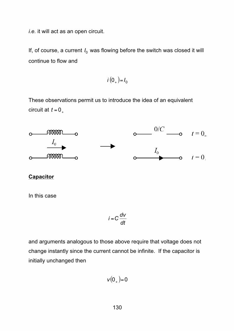
i.e. it will act as an open circuit.
If, of course, a current 0I was flowing before the switch was closed it will
continue to flow and
( ) 00 Ii =+
These observations permit us to introduce the idea of an equivalent
circuit at += 0t
Capacitor
In this case
dtdvCi =
and arguments analogous to those above require that voltage does not
change instantly since the current cannot be infinite. If the capacitor is
initially unchanged then
( ) 00 =+v
Circuit Analysis II WRM MT11
131
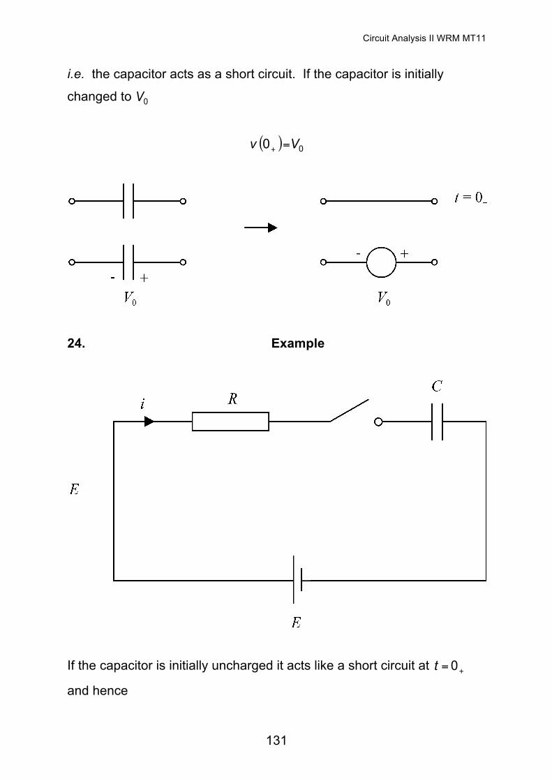
i.e. the capacitor acts as a short circuit. If the capacitor is initially
changed to 0V
( ) 00 Vv =+
24. Example
If the capacitor is initially uncharged it acts like a short circuit at += 0t
and hence
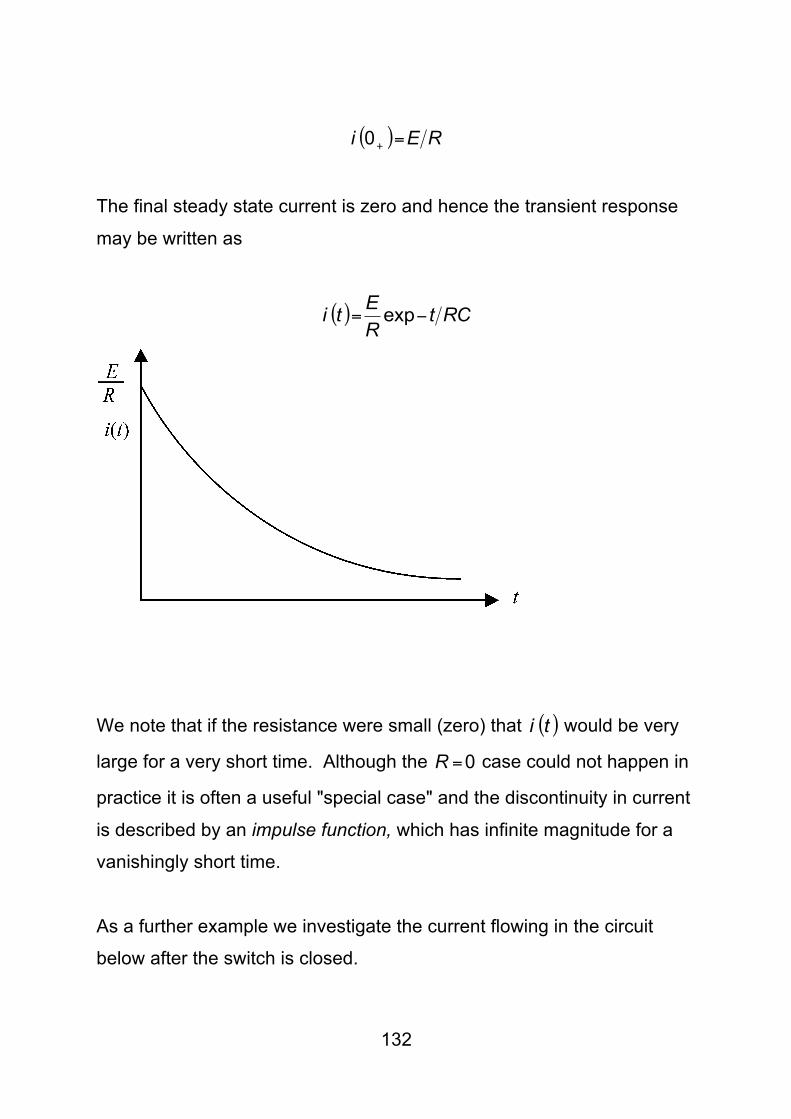
132
( ) REi =+0
The final steady state current is zero and hence the transient response
may be written as
( ) RCtREti −= exp
We note that if the resistance were small (zero) that ( )ti would be very
large for a very short time. Although the 0=R case could not happen in
practice it is often a useful "special case" and the discontinuity in current
is described by an impulse function, which has infinite magnitude for a
vanishingly short time.
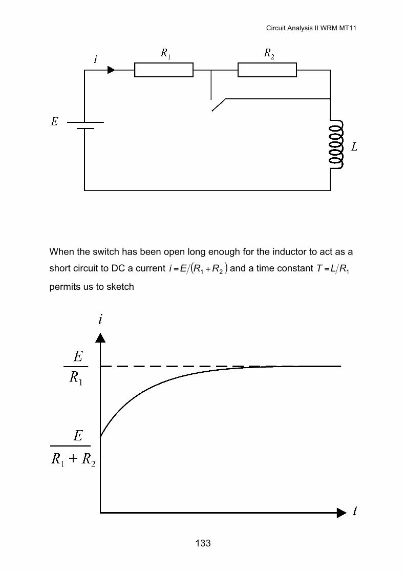
As a further example we investigate the current flowing in the circuit
below after the switch is closed.
Circuit Analysis II WRM MT11
133
When the switch has been open long enough for the inductor to act as a
short circuit to DC a current ( )21 RREi += and a time constant 1RLT =
permits us to sketch
134
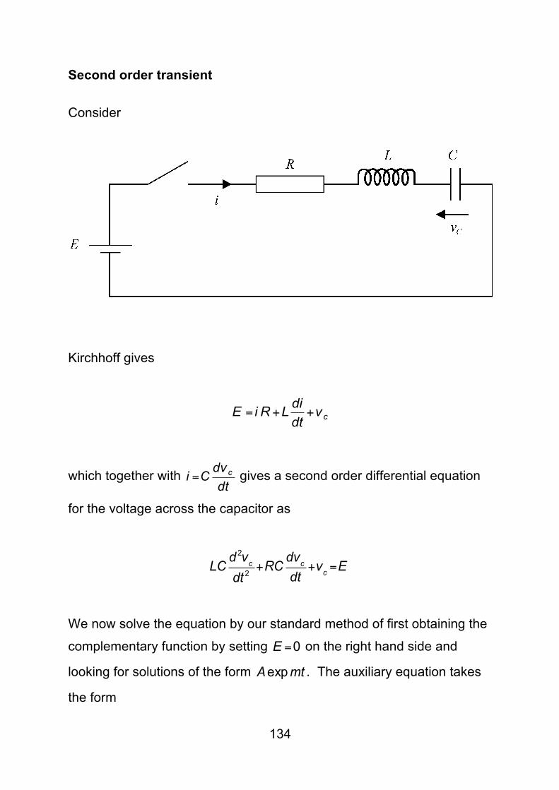
Second order transient
Consider
Kirchhoff gives
cvdtdiLRiE ++=
which together with dtdv
Ci c= gives a second order differential equation
for the voltage across the capacitor as
LCd 2vcdt 2
+RCdvcdt
+vc =E
We now solve the equation by our standard method of first obtaining the
complementary function by setting 0=E on the right hand side and
looking for solutions of the form mtAexp . The auxiliary equation takes
the form
Circuit Analysis II WRM MT11
135
012 =++ mRCmLC
which has solutions
LCLR
LRm 1
42 2
2
−±−=
In order to make some general comments we now recast this into non
circuit-specific notation following our discussion of resonance. In that
context we introduced
RLQ
LC0
01 ω
==ω and
We also noted that Q was related to the damping factor
LCR
Q 221==ζζ via . This permits us to write
⎟⎠⎞⎜
⎝⎛ −ζ±ζ−ω= 10
2m
or
β±α−=m
with ζω=α 0 and 120 −ζω=β .
136
We note that the particular integral, - corresponding to the steady value
of vc – is simply Evc = . The full solution is therefore
{ } ttBtAEvc α−β−+β+= expexpexp
where the unknown constants are determined by the initial conditions,
0=cv and 0=i . We note that the latter condition is formally equivalent
to requiring 0=dtdvc . The full solution now takes the form
( ){ ( ) } tttEEvc α−β−α−β+βα+ββ
−= expexpexp2
It is clear that according to the value of ζ the factor β may be real or
imaginary. We consider these cases in turn
Case 1: ζ >1; R>2 L C
In this case β is real and α>β. It is convenient to write the solution
as
( ) ( ){ ( ) ( ) }ttEEvc β+αβ−α−β−α−β+αβ
−= expexp2
where we see that the transient solution of the response is the difference
between two exponentials and is negative. The voltage cv follows the
Circuit Analysis II WRM MT11
137
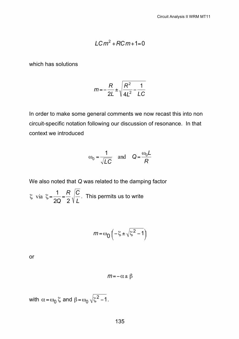
usual gradual rise to its steady state value typical over overdamped
systems.
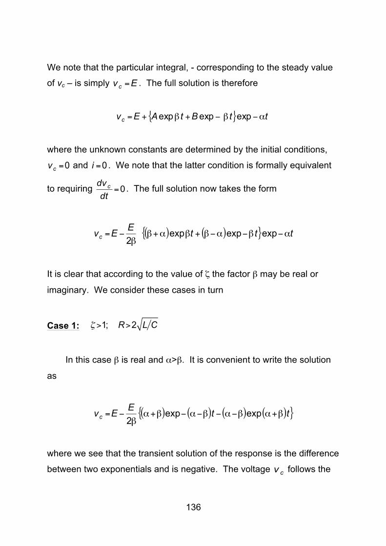
We note that the current is given by
dtdv
Ci c=
or
( ) ( ){ }ttEC
i β+α−−β−α−β
ω= expexp
2
20
Thus the current is proportional to the difference in two exponentials of
equal amplitude but different decay rates and hence rises from zero to a
maximum before finally falling to its steady state value of zero
138
Case 2: ζ =1 ; R=2 L C
For this special case of critical damping the general solution is no longer
valid since the auxiliary equation has two equal roots. The
complementary function in this case must take the form
( ) tDtC 0exp ω−+
and hence the full solution becomes
( ) tDtCEvc 0exp ω−++=
which with initial conditions 0== iv c gives
( ){ }ttEvc 00 exp11 ω−ω+−=
which gives a response graphically similar to the previous case.
Circuit Analysis II WRM MT11
139
Case 3: ζ <1 ; R<2 L C
In this case β becomes imaginary and so we write
njj ω=ζ−ω=−ζω=β 20
20 11
with
2
0 1 ζ−ω=ωn
It is now straightforward to recast the general solution of page 131 by
replacing β with nj ω as
⎭⎬⎫
⎩⎨⎧
α−⎟⎟⎠
⎞⎜⎜⎝
⎛ω
ω
α+ω−= tttEv n
nnc expsincos1
In this case the solution is very different from before. The transient
solution is oscillatory, at a frequency nω , but its amplitude decays at a
rate determined by ( )0ωζ=α and we speak of underdamped oscillation.
The frequency 20 1 ζ−ω=ωn is the natural frequency. The same term
is sometimes applied to 0ω but since the two are strictly only equal when
1=ζ (critical damping)
140
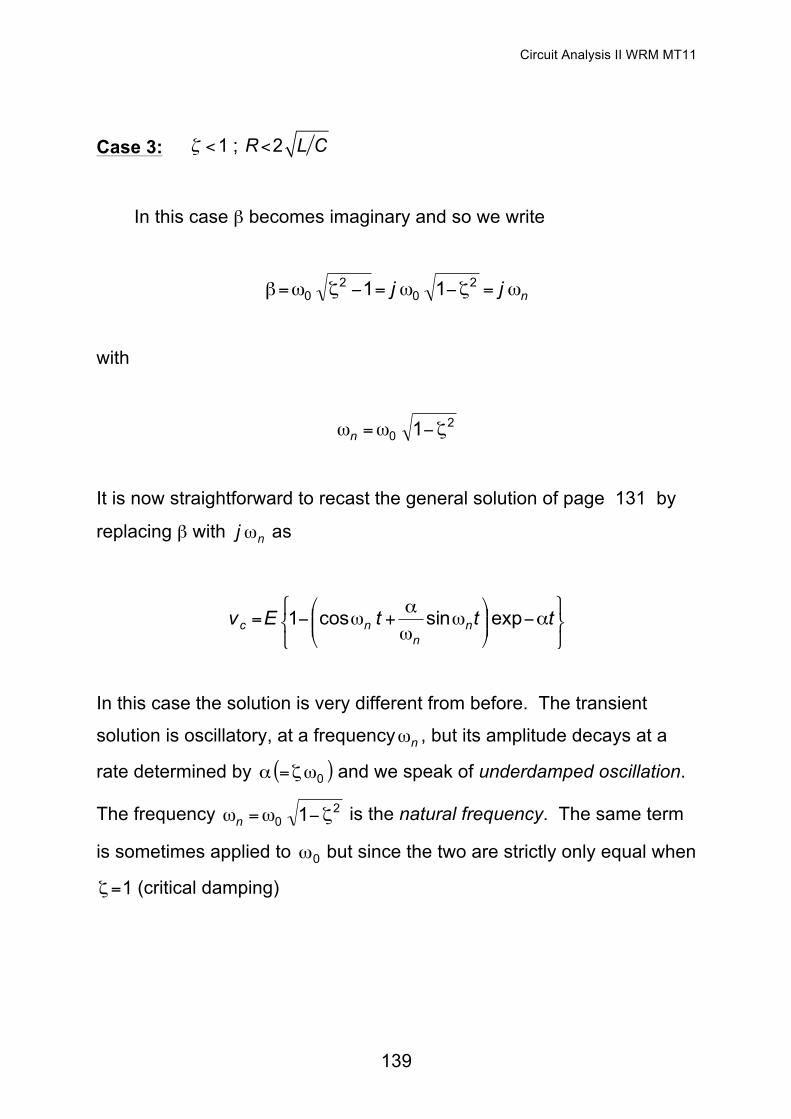
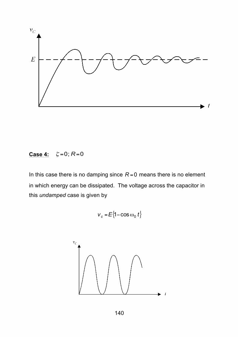
Case 4: ζ =0;R=0
In this case there is no damping since 0=R means there is no element
in which energy can be dissipated. The voltage across the capacitor in
this undamped case is given by
{ }tEvc 0cos1 ω−=
Circuit Analysis II WRM MT11
141
We observe that for small damping, representing minimal loss, that the
frequency of the oscillatory transient 02
0 1 ω≈ζ−ω=ωn , the resonance
frequency in the steady state. This is not surprising since this is the
frequency at which energy naturally oscillates between the reactive
elements and this is actually what is happening during transient
oscillation. Naturally with increased damping the effect is reduced.
We therefore see that the damping factor ζ (or Q) has an important role
in describing the transient behaviour:
If the damping is less than critical (ζ<1) the transient
behaviour is oscillatory otherwise it is not.
142
25. The Laplace Transform
The classical approach we have just used to find the transient response
and indeed the final steady state response for simple circuits may be
extended to ever more involved circuits but at the expense of ridiculously
increased complexity. An alternative approach is required. Since we
are concerned with turning forcing functions, often constants, on and off
the mathematical technique of choice to solve the differential equations
is based on the use of the Laplace transform. This is particularly useful
for our purposes because
(i) it gives rise to the ability to write circuit equations in a very general
way just as the "jω" method does for sinusoidal forcing functions.
(ii) the initial conditions are dealt with automatically. The solution does
not contain any arbitrary constants.
(iii) Transients are dealt with automatically.
(iv) and, very importantly, the answers can be looked up easily in
H.L.T.!!
We recall that the Laplace transform of a function of time ( )tf is
defined as
( ){ } ( ) ( ) dtsttfsFtfL −== ∫∞
exp0
Circuit Analysis II WRM MT11
143
where negative values of t are excluded. In mathematics since only
positive values of the variable t are permitted this is often called 'one-
sided' transform.
Arguably one of the most useful properties, from our point of view, of the
Laplace transform, is that for a given ( )tf there is one and only one
( )sF and vice versa ( )sF and ( )tf are called transform pairs.
( ) ( )tfsF ↔
Hence if we know the value of ( )sF and we want to know ( )tf , or vice
versa, we simply look it up in the tables!! What could be easier?
Although you will have worked out Laplace transforms in maths we'll
introduce a few 'electrically useful' transform pairs below.
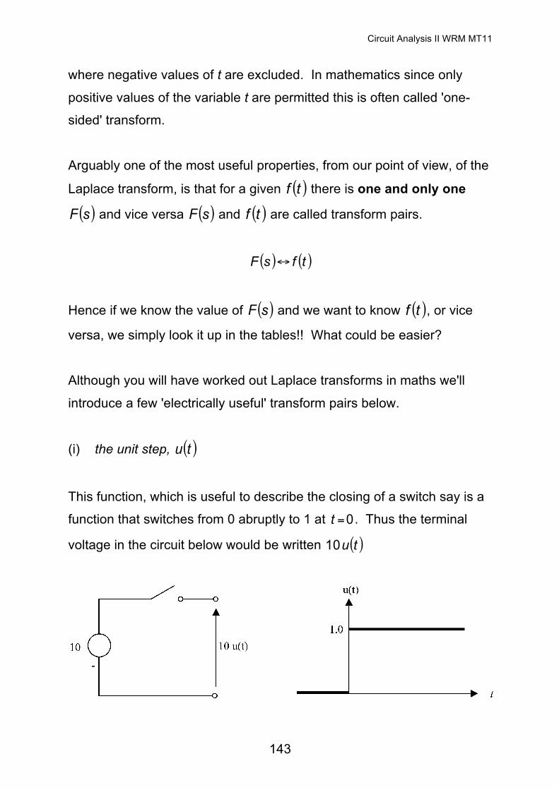
(i) the unit step, ( )tu
This function, which is useful to describe the closing of a switch say is a
function that switches from 0 abruptly to 1 at 0=t . Thus the terminal
voltage in the circuit below would be written ( )tu10
144
The Laplace transform ( )sU is given by
( ) ( )s
dtstdtsttusU 1exp1exp00
=−=−= ∫∫∞∞
Hence
( )s
tu 1↔
are Laplace transform pairs. Thus given ( )s
sU 1= the corresponding
function of time is the unit step, ( )tu .
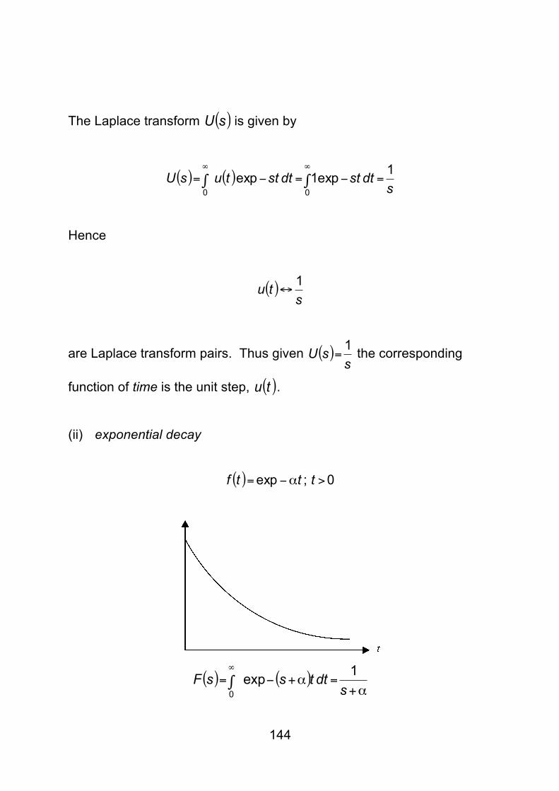
(ii) exponential decay
( ) 0;exp >α−= tttf
( ) ( )α+
=α+−= ∫∞
sdttssF 1exp
0
Circuit Analysis II WRM MT11
145
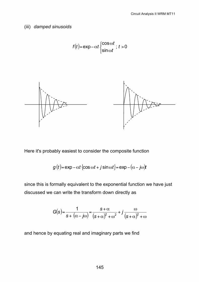
(iii) damped sinusoids
( ) 0;sincos
exp >⎩⎨⎧
ω
ωα−= t
tt
ttf
Here it's probably easiest to consider the composite function
( ) { } ( )tjtjtttg ω−α−=ω+ωα−= expsincosexp
since this is formally equivalent to the exponential function we have just
discussed we can write the transform down directly as
( )( ) ( ) ( ) ω+α+
ω+
ω+α+
α+=
ω−α+= 222
1s
jss
jssG
and hence by equating real and imaginary parts we find
146
{ }( )
{ }( ) 2222 sinexp;cosexp
ω+α+
ω=ωα−
ω+α+
α+=ωα−
sttL
ssttL
(iv) Laplace transform of a derivative
If the Laplace transform of ( )tf is ( )sF then
( ) ( )+−=⎭⎬⎫
⎩⎨⎧ 0fsFsdtdfL
Where ( )+0f represents the initial value of ( )tf . The corresponding
expressions for the second derivative is
( ) ( ) ( )++ ʹ′−−=⎭⎬⎫
⎩⎨⎧
0022
2
ffssFsdtfdL
where ( )⋅f denotes the first derivative.
Fortunately for you in the P2 course (though not in the P1 course), we
will only use Laplace in the case of zero initial conditions when these
expressions simplify to
( )sFsdtdfL =
⎭⎬⎫
⎩⎨⎧
and ( )sFs
dtfdL 22
2
=⎭⎬⎫
⎩⎨⎧
(v) Laplace transform of an integral
( ) ( )ssFdttfL
t=⎭⎬⎫
⎩⎨⎧∫0
Circuit Analysis II WRM MT11
147
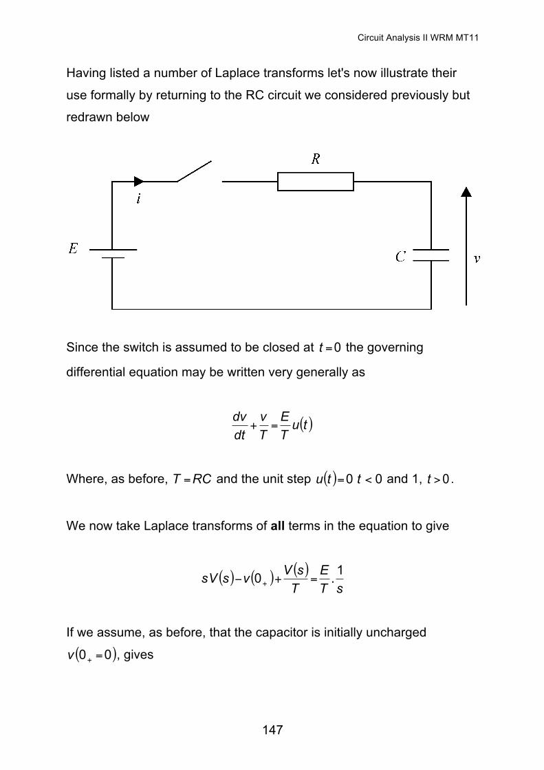
Having listed a number of Laplace transforms let's now illustrate their
use formally by returning to the RC circuit we considered previously but
redrawn below
Since the switch is assumed to be closed at 0=t the governing
differential equation may be written very generally as
( )tuTE
Tv
dtdv
=+
Where, as before, RCT = and the unit step ( ) 00 <= ttu and 1, 0>t .
We now take Laplace transforms of all terms in the equation to give
( ) ( ) ( )sT
ETsVvsVs 1.0 =+− +
If we assume, as before, that the capacitor is initially uncharged
( )00 =+v , gives
148
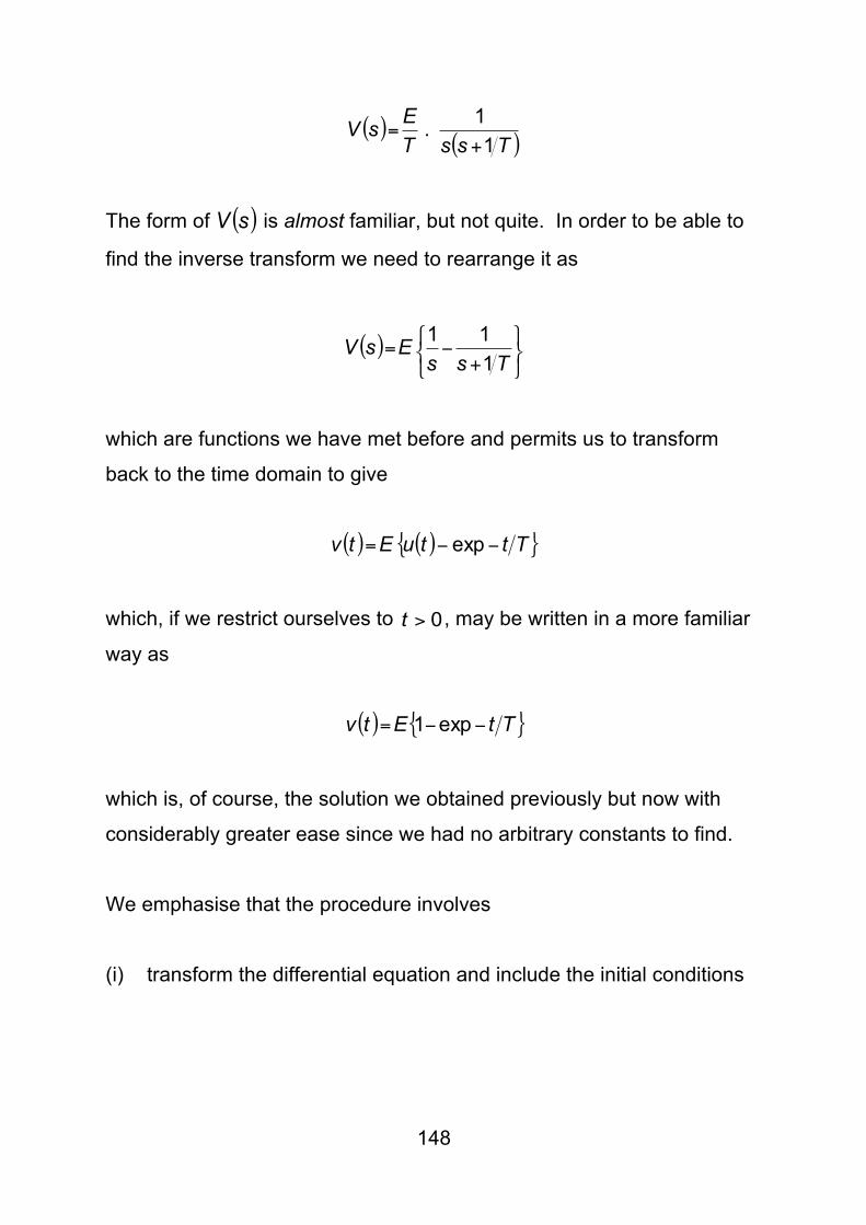
( )( )TssT
EsV11.+
=
The form of ( )sV is almost familiar, but not quite. In order to be able to
find the inverse transform we need to rearrange it as
( )⎭⎬⎫
⎩⎨⎧
+−=
TssEsV
111
which are functions we have met before and permits us to transform
back to the time domain to give
( ) ( ){ }TttuEtv −−= exp
which, if we restrict ourselves to 0>t , may be written in a more familiar
way as
( ) { }TtEtv −−= exp1
which is, of course, the solution we obtained previously but now with
considerably greater ease since we had no arbitrary constants to find.
We emphasise that the procedure involves
(i) transform the differential equation and include the initial conditions
Circuit Analysis II WRM MT11
149
(ii) manipulate the equation to obtain ( )sV is an easily 'invertible' form.
This, sadly, may involve the use of partial fractions in more involved
cases.
(iii) transform back to the time domain to obtain ( )tv .
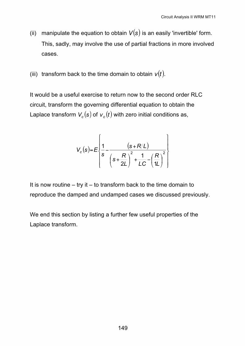
It would be a useful exercise to return now to the second order RLC
circuit, transform the governing differential equation to obtain the
Laplace transform ( )sVc of ( )tvc with zero initial conditions as,
( ) ( )
⎪⎪
⎭
⎪⎪
⎬
⎫
⎪⎪
⎩
⎪⎪
⎨
⎧
⎟⎠
⎞⎜⎝
⎛−+⎟⎠
⎞⎜⎝
⎛ +
+−= 22
11
2
1
LR
LCLRs
LRss
EsVc
It is now routine – try it – to transform back to the time domain to
reproduce the damped and undamped cases we discussed previously.
We end this section by listing a further few useful properties of the
Laplace transform.
150
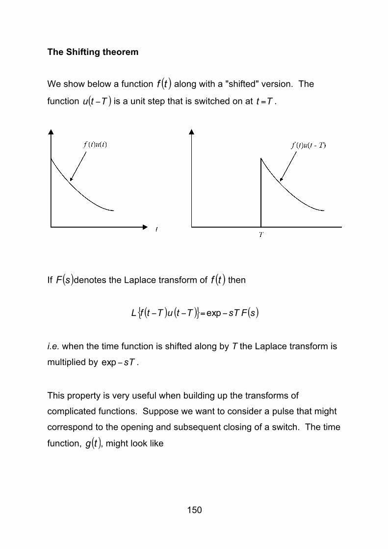
The Shifting theorem
We show below a function ( )tf along with a "shifted" version. The
function ( )Ttu − is a unit step that is switched on at Tt = .
If ( )sF denotes the Laplace transform of ( )tf then
( ) ( ){ } ( )sFsTTtuTtfL −=−− exp
i.e. when the time function is shifted along by T the Laplace transform is
multiplied by sT−exp .
This property is very useful when building up the transforms of
complicated functions. Suppose we want to consider a pulse that might
correspond to the opening and subsequent closing of a switch. The time
function, ( )tg , might look like
Circuit Analysis II WRM MT11
151
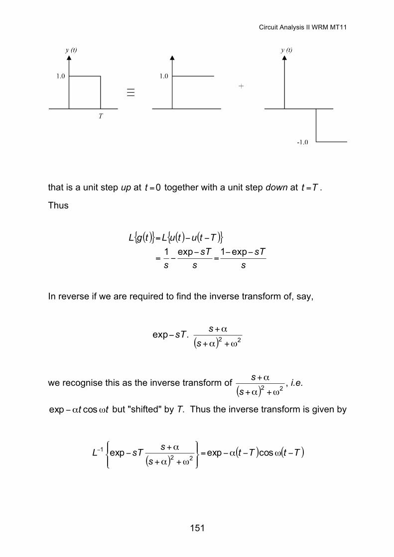
that is a unit step up at 0=t together with a unit step down at Tt = .
Thus
( ){ } ( ) ( ){ }
ssT
ssT
s
TtutuLtgL−−
=−
−=
−−=
exp1exp1
In reverse if we are required to find the inverse transform of, say,
( ) 22.expω+α+
α+−
sssT
we recognise this as the inverse transform of ( ) 22 ω+α+
α+
ss , i.e.
tt ωα− cosexp but "shifted" by T. Thus the inverse transform is given by
( )( ) ( )TtTt
sssTL −ω−α−=
⎪⎭
⎪⎬⎫
⎪⎩
⎪⎨⎧
ω+α+
α+−− cosexpexp
221
152
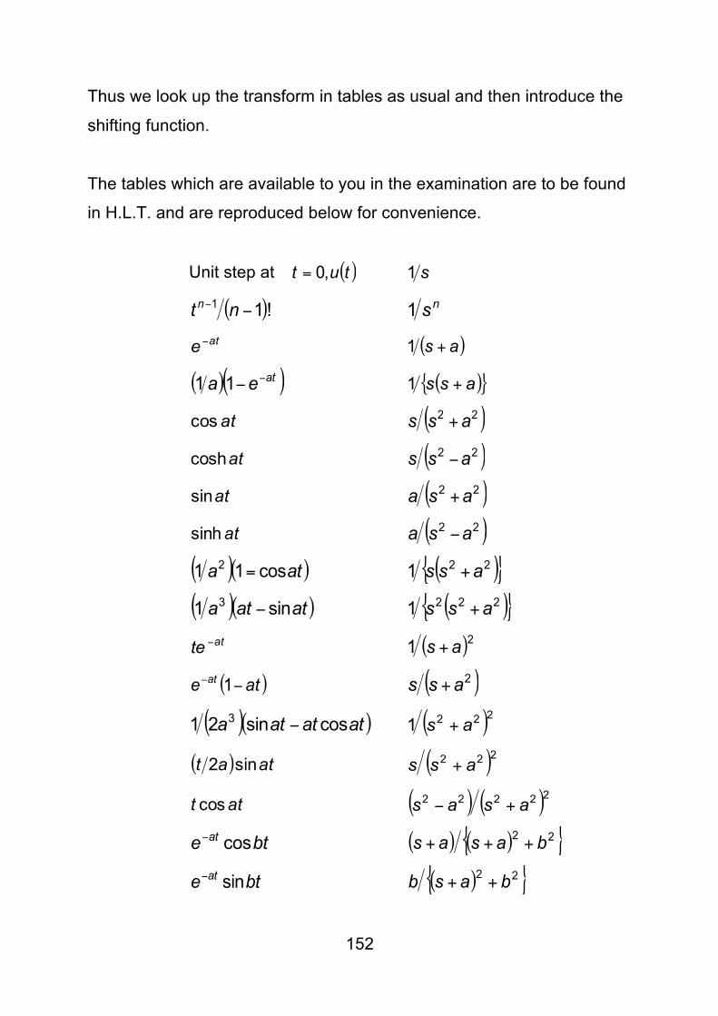
Thus we look up the transform in tables as usual and then introduce the
shifting function.
The tables which are available to you in the examination are to be found
in H.L.T. and are reproduced below for convenience.
Unit step at ( )tut ,0= s1
( )!11 −− ntn ns1
ate− ( )as +1
( )( )atea −−11 ( ){ }ass +1
atcos ( )22 ass +
atcosh ( )22 ass −
atsin ( )22 asa +
atsinh ( )22 asa −
( )( )ata cos11 2 = ( ){ }221 ass +
( )( )atata sin1 3 − ( ){ }2221 ass +
atte − ( )21 as +
( )ate at −− 1 ( )2ass +
( )( )atatata cossin21 3 − ( )2221 as +
( ) atat sin2 ( )222 ass +
att cos ( ) ( )22222 asas +−
bte at cos− ( ) ( ){ }22 basas +++
bte at sin− ( ){ }22 basb ++
Circuit Analysis II WRM MT11
153
26. The Laplace transform in circuit analysis. If we wanted to find how the voltage across a certain component varied
with time due to some arbitrary forcing function it would be perfectly
possible, using appropriate combinations of node-voltage and loop
equations, to set up the required (simultaneous) differential equations.
We could then take Laplace transforms of both sides of all the equations
or, to put it more technically, we would transform from the time domain
to the s-domain. The resulting simultaneous algebraic equations could
then be solved to find an expression for the Laplace transform of the
desired ‘output’ in terms of the Laplace transform of the ‘input’ source.
Once this frequency response function has been obtained it becomes a
routine matter to introduce the actual transform of the source and then
transform back to the time domain by looking up the inverse transforms
in tables. However it is possible to miss out the initial steps of writing the
differential equations and transforming them by working directly with
transformed voltages and currents V(s) and I(s) together with the
appropriate s-domain version of ‘Ohm’s Law’ for resistors, capacitors
and inductors.
Representation of circuit elements in the s-domain.
Resistor
The v-i equation for a resistor in the time domain is
iRv =
154
The Laplace transform of this equation is
)()( sIRsV =
The transfer function RsZsIsV == )()(/)( is the s-domain impedance
of the element.
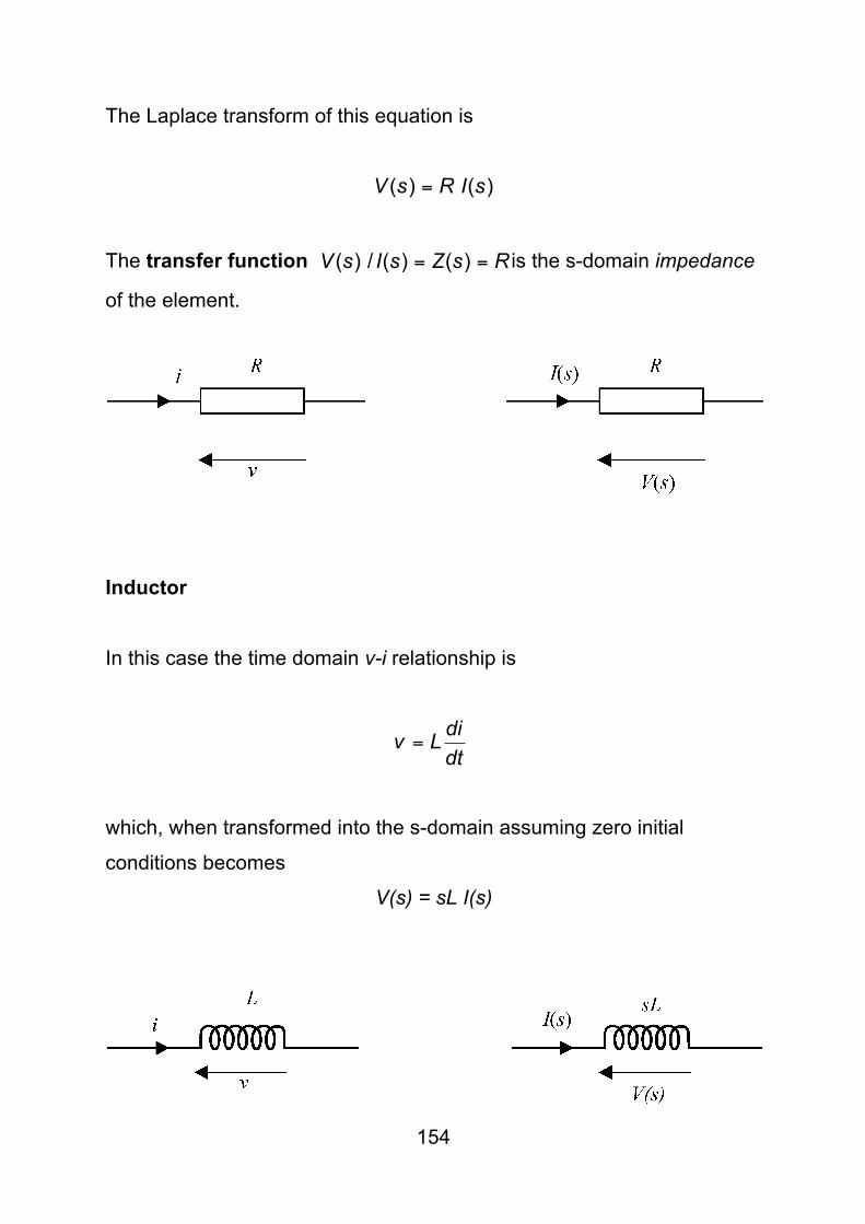
Inductor
In this case the time domain v-i relationship is
dtdiLv =
which, when transformed into the s-domain assuming zero initial
conditions becomes
V(s) = sL I(s)
Circuit Analysis II WRM MT11
155
Capacitor
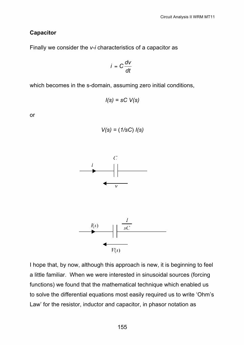
Finally we consider the v-i characteristics of a capacitor as
dtdvCi =
which becomes in the s-domain, assuming zero initial conditions,
I(s) = sC V(s)
or
V(s) = (1/sC) I(s)
I hope that, by now, although this approach is new, it is beginning to feel
a little familiar. When we were interested in sinusoidal sources (forcing
functions) we found that the mathematical technique which enabled us
to solve the differential equations most easily required us to write ‘Ohm’s
Law’ for the resistor, inductor and capacitor, in phasor notation as
156
ICj1VandILjVIRVω
=ω==
respectively. In the more general s-domain case the relationships are
IsC1VandIsLVIRV ===
which are seen to be identical if we merely replace jω by s. Thus all
the methods we developed in the AC theory ‘jω’ case carry over to the s-
domain by simple substitution.
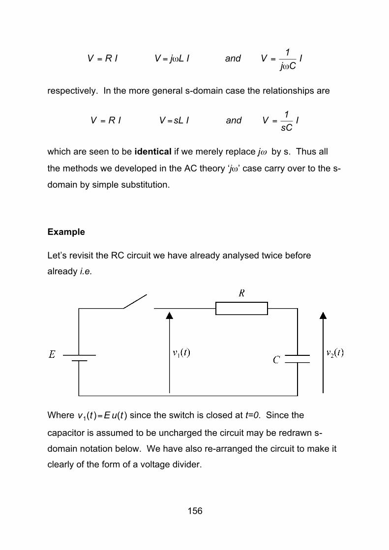
Example
Let’s revisit the RC circuit we have already analysed twice before
already i.e.
Where )()(1 tuEtv = since the switch is closed at t=0. Since the
capacitor is assumed to be uncharged the circuit may be redrawn s-
domain notation below. We have also re-arranged the circuit to make it
clearly of the form of a voltage divider.
Circuit Analysis II WRM MT11
157
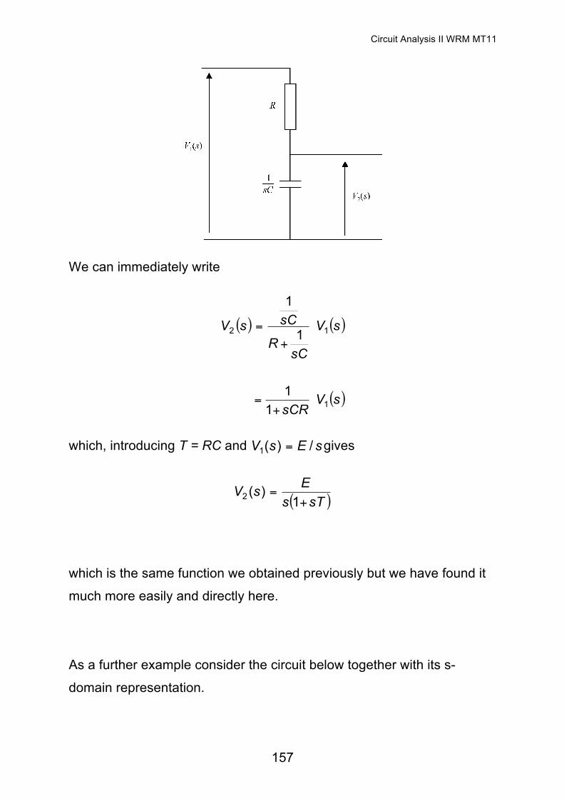
We can immediately write
( ) ( )
( )sVsCR
sV
sCR
sCsV
1
12
11
1
1
+=
+=
which, introducing T = RC and sEsV /)(1 = gives
( )sTsEsV+
=1
)(2
which is the same function we obtained previously but we have found it
much more easily and directly here.
As a further example consider the circuit below together with its s-
domain representation.
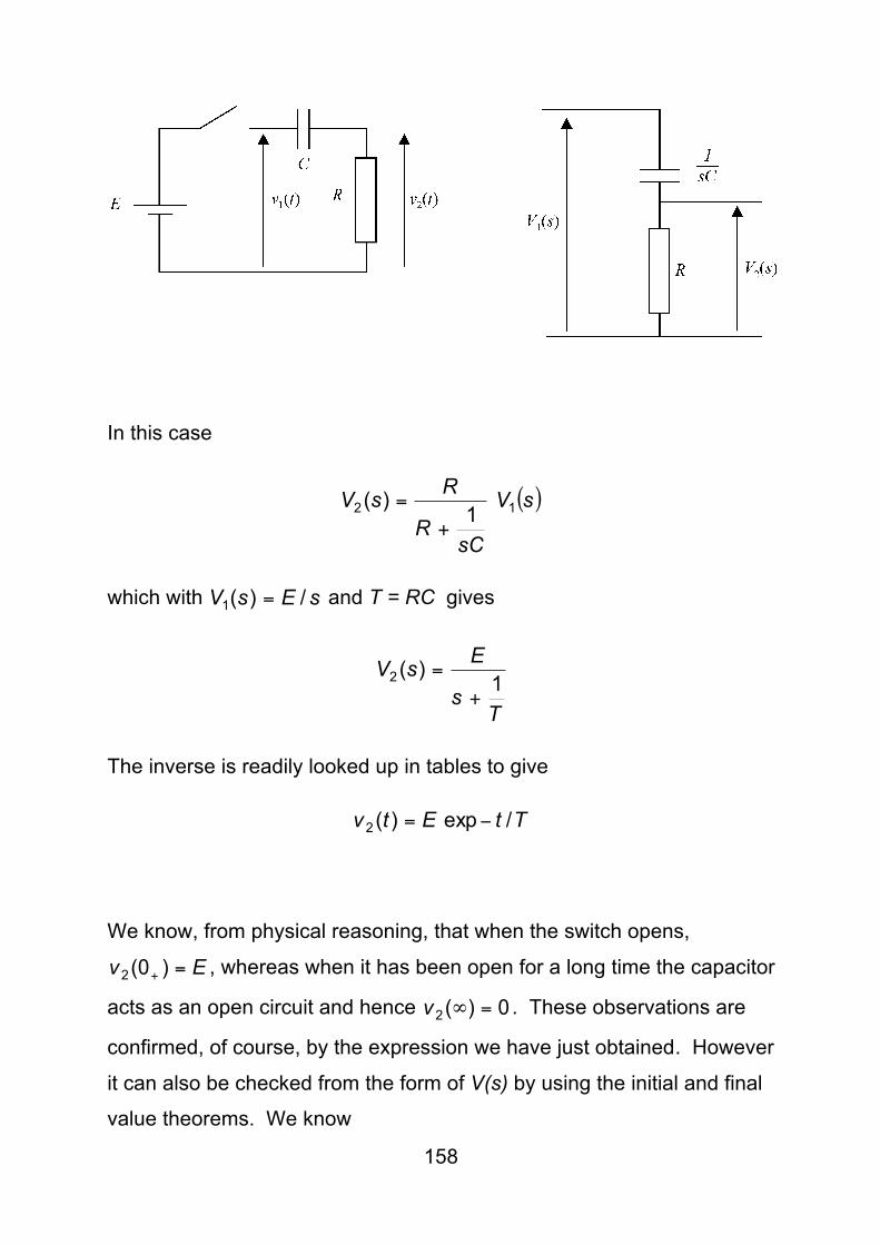
158
In this case
( )sV
sCR
RsV 12 1)(
+=
which with sEsV /)(1 = and T = RC gives
Ts
EsV1
)(2+
=
The inverse is readily looked up in tables to give
TtEtv /exp)(2 −=
We know, from physical reasoning, that when the switch opens,
Ev =+ )0(2 , whereas when it has been open for a long time the capacitor
acts as an open circuit and hence 0)(2 =∞v . These observations are
confirmed, of course, by the expression we have just obtained. However
it can also be checked from the form of V(s) by using the initial and final
value theorems. We know
Circuit Analysis II WRM MT11
159
{ } EsT
ELim
Ts
sELimssVLimvalue initial sss =⎭⎬⎫
⎩⎨⎧
+=
⎪⎭
⎪⎬
⎫
⎪⎩
⎪⎨
⎧
+== ∞→∞→∞→ 11
)(2
whereas the final value is given by
{ } 01
)( 020 =⎪⎭
⎪⎬
⎫
⎪⎩
⎪⎨
⎧
+== →→
Ts
sELimssVLimvalue final ss
We note the procedure is
(i) Introduce ‘generalised’ s-domain impedances, sL and 1/sC.
(ii) Find the appropriate transfer function. In more complicated cases
this may/will involve writing node-voltage and/or loop equations.
(iii) Substitute the Laplace transform of the input signal (forcing
function)
(iv) Convert back to the time domain by looking up the inverse
transforms in tables.
As a final example let’s consider the following circuit where the input
voltage is a pulse of duration T and we are required to find the voltage
)(2 tv .
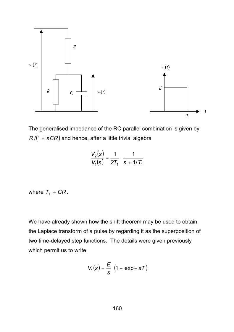
160
The generalised impedance of the RC parallel combination is given by
( )CRsR +1/ and hence, after a little trivial algebra
( )( ) 111
2
/11
21
TsTsVsV
+=
where CRT =1 .
We have already shown how the shift theorem may be used to obtain
the Laplace transform of a pulse by regarding it as the superposition of
two time-delayed step functions. The details were given previously
which permit us to write
( ) ( )sTsEsV −−= exp11
Circuit Analysis II WRM MT11
161
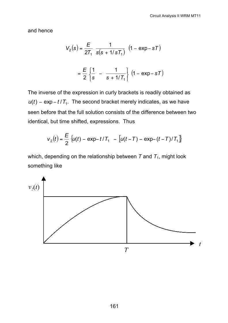
and hence
( )( )
( )
( )sTTss
E
sTsTssT
EsV
−−⎭⎬⎫
⎩⎨⎧
+−=
−−+
=
exp1/111
2
exp1/11
2
1
112
The inverse of the expression in curly brackets is readily obtained as
1/exp)( Tttu −− . The second bracket merely indicates, as we have
seen before that the full solution consists of the difference between two
identical, but time shifted, expressions. Thus
( ) [ ]{ }112 /)(exp)(/exp)(2
TTtTtuTttuEtv −−−−−−−=
which, depending on the relationship between T and T1, might look
something like

162
27. Disclaimer!!
The notes are reasonably self-contained but they certainly don’t pretend
to tell the whole story so do consult one or more of the huge number of
textbooks on the subject.
If you spot any errors, do please tell me: [email protected].