Embed Size (px)
Citation preview

S f Ch i iSurface Characterization
LEED
PhotoemissionPhotoemission
Linear optics

Surface characterization with electrons
M P S h WA D h S f I t f A l 1 (1979) 2M.P. Seah, W.A. Dench, Surf. Interf. Anal. 1 (1979) 2
LEED low energy electron diffractionLEED – low energy electron diffractionDe Broglie wavelength: λ= h/(mv)g g /( )For electrons: λ = 150 / E0 E0 in eV, λ in Å.For 100 eV‐electrons: λ(100) = 1.22 Å (low energy)Corresponds to atomic dimensions, similar to XRD

Analogy to optical grating.
Constructive interference:Enhancement of intensity only
a ogy to opt ca g at g
y yin certain directions:
n λ = d sinθn λ d sinθ
For 2D arrangement (plane lattice):scattering conditions have to bescattering conditions have to befulfilled in both directions.
h,k(order)
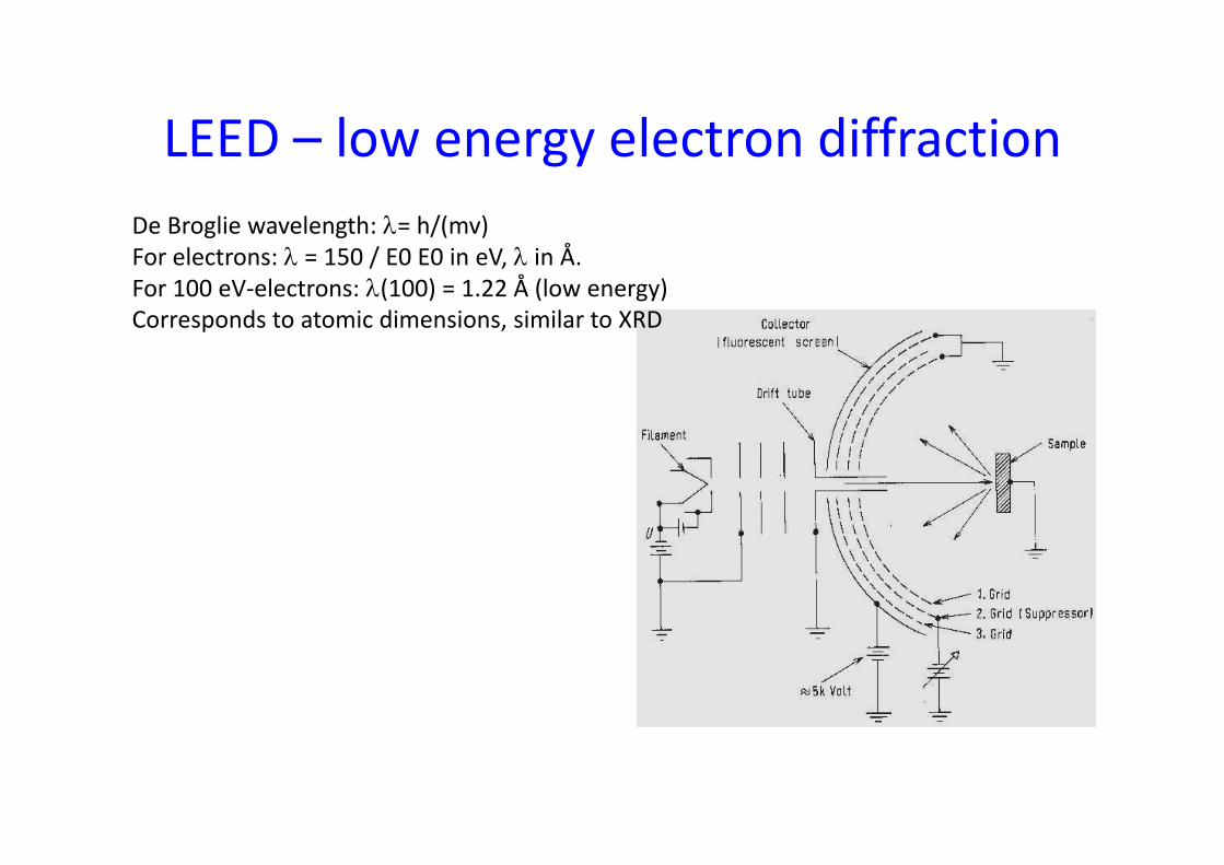
20 ML Ge
Ge onSi(111)7 7Si(111)7x7
Transition from 7x7 to 5x5
Si(111)7x7
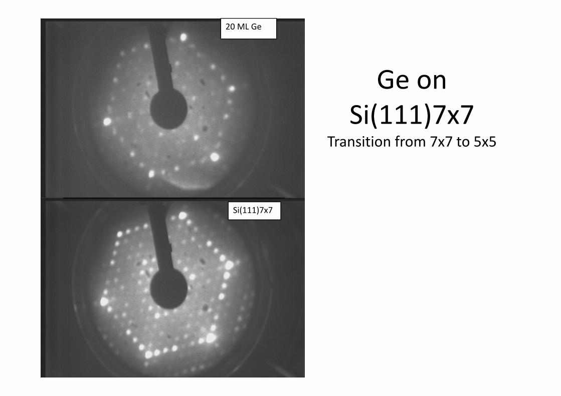
Synchrotron radiation photoemission spectroscopy
• ISA Aarhus University• ISA Aarhus University• Maximum Energy 580 MeV• Max Current 250 mA
Lif ti 15 h• Lifetime 15 hours
SGM130‐400 eV1010 photons/sec @130 eV

Photoelectron spectroscopy• Core levels
– Chemical reactions/mixing
– Growth modesGrowth modes
• Valence bands– Electronic levels relevant for optics
hν=130 eV
hν
arb.
uni
ts) Al2p
sp bandSecondary
Inte
nsity
(a
Binding Energy(eV)
Secondaryelectrons
EF Evac Kinetic Energy (eV)g gy( ) gy ( )
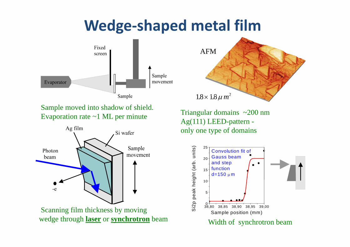
Wedge‐shaped metal filmAFM
18 18 218 18 2. .× μmSample moved into shadow of shield. Evaporation rate ~1 ML per minute Triangular domains ~200 nm
Ag(111) LEED-pattern -Ag(111) LEED pattern only one type of domains
25Convolution fit ofts
)
15
20
Convolution fit ofGauss beamand step functiond=150 μm
ght (
arb.
uni
S i fil hi k b i 38,80 38,85 38,90 38,95 39,000
5
10
i2p
peak
hei
Scanning film thickness by movingwedge through laser or synchrotron beam
38,80 38,85 38,90 38,95 39,00
Si
Sample position (mm)
Width of synchrotron beam
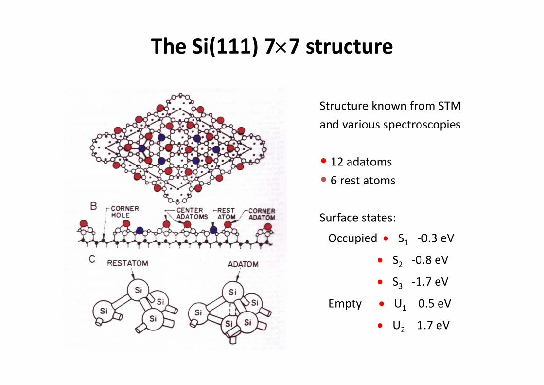
The Si(111) 7×7 structure
Structure known from STMStructure known from STM
and various spectroscopies
• 12 adatoms
• 6 rest atoms
Surface states:
Occupied • S 0 3 eVOccupied • S1 ‐0.3 eV
• S2 ‐0.8 eV
• S 1 7 eV• S3 ‐1.7 eV
Empty • U1 0.5 eV
• U 1 7 eV• U2 1.7 eV
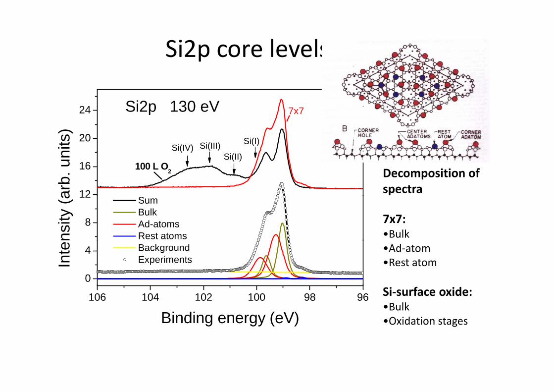
Si2p core levels
24 Si2p 130 eV
20
24
Si(I)Si(III)Si(IV)
7x7Si2p 130 eV
nits
)
12
16Si(II)
( )
arb.
un
100 L O2 Decomposition ofspectra
8
12 Sum Bulk Ad-atoms Rest atomsns
ity (a
7x7:•Bulk
0
4 Background ExperimentsInte •Ad‐atom
•Rest atom
106 104 102 100 98 96
Binding energy (eV)
Si‐surface oxide:•Bulk•Oxidation stages
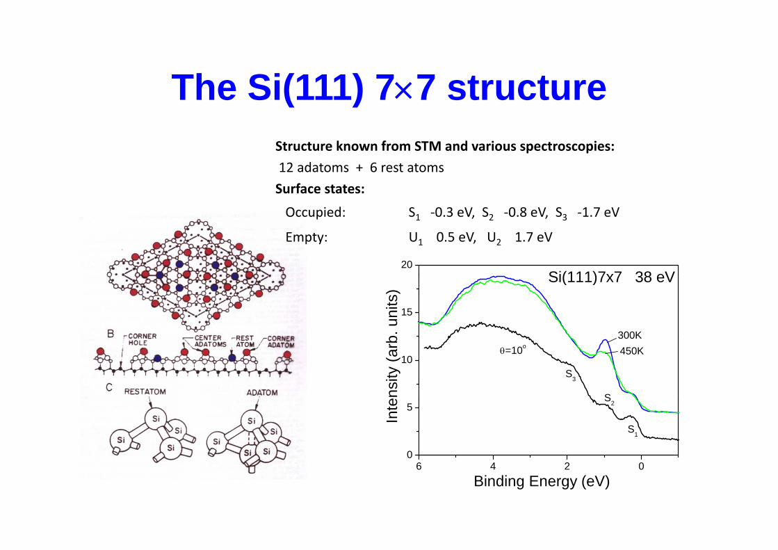
The Si(111) 7×7 structureThe Si(111) 7×7 structureStructure known from STM and various spectroscopies:Structure known from STM and various spectroscopies:
12 adatoms + 6 rest atoms
Surface states:
Occupied: S ‐0 3 eV S ‐0 8 eV S ‐1 7 eVOccupied: S1 ‐0.3 eV, S2 ‐0.8 eV, S3 ‐1.7 eV
Empty: U1 0.5 eV, U2 1.7 eV
20Si(111)7x7 38 eV
15
b. u
nits
)
300K
Si(111)7x7 38 eV
10
ensi
ty (a
rbS
S3
300K450Kθ=10o
6 4 2 00
5In
te
S1
S2
6 4 2 0Binding Energy (eV)
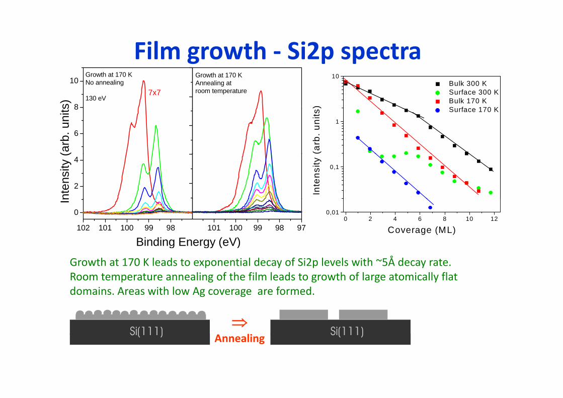
Film growth ‐ Si2p spectrag p p
8
10Growth at 170 KNo annealing
130 eV
s)
7x7
Growth at 170 KAnnealing atroom temperature
10 Bulk 300 K Surface 300 K Bulk 170 KSurface 170 K)
6
8
(arb
. uni
ts
1
Surface 170 K
(arb
. uni
ts
2
4
nten
sity
(
0,1
Inte
nsity
102 101 100 99 98
0
101 100 99 98 97
In
Binding Energy (eV)
0 2 4 6 8 10 120,01
Coverage (ML)Binding Energy (eV)
Growth at 170 K leads to exponential decay of Si2p levels with ~5Å decay rate.Room temperature annealing of the film leads to growth of large atomically flatdomains Areas with low Ag coverage are formeddomains. Areas with low Ag coverage are formed.
⇒A liAnnealing
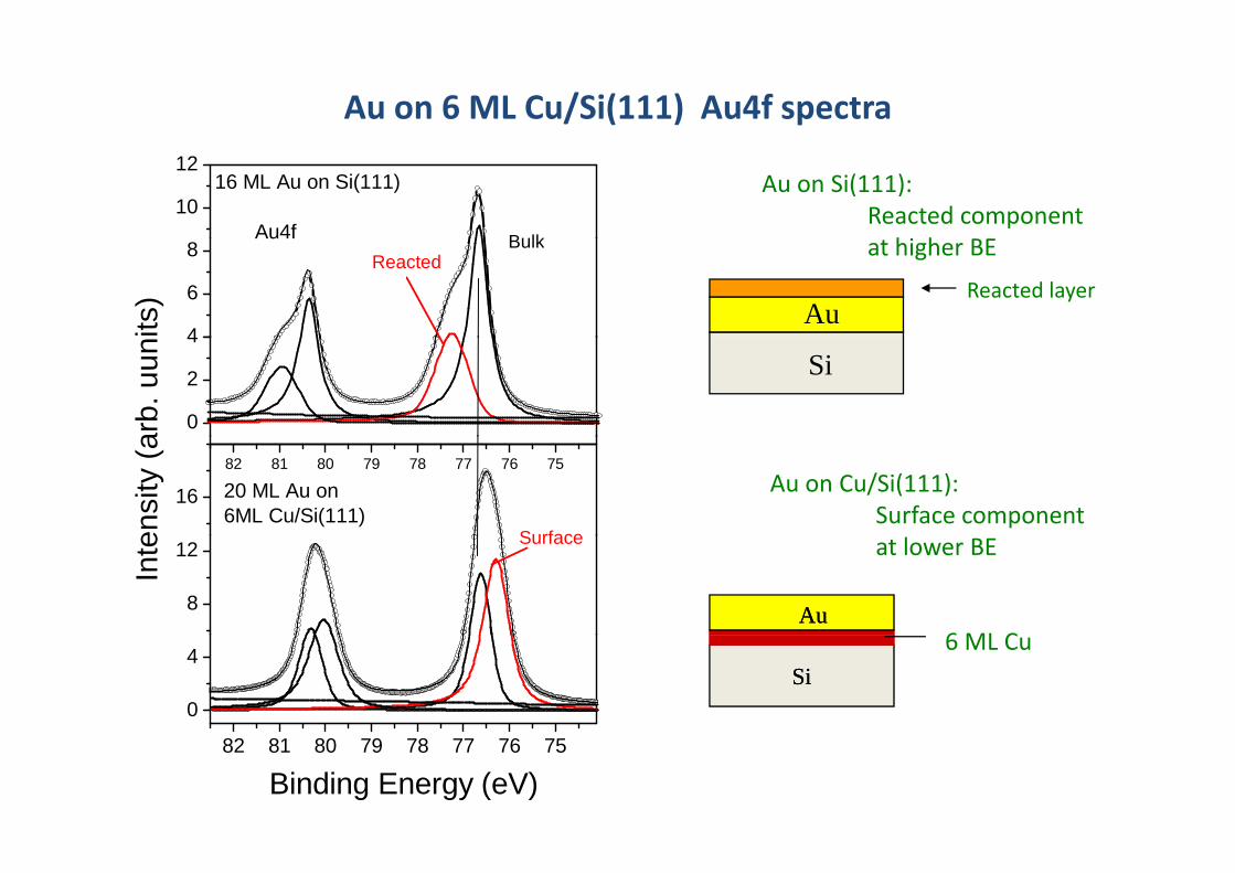
Au on 6 ML Cu/Si(111) Au4f spectra
10
1216 ML Au on Si(111)
Au4f Bulk
Au on Si(111):Reacted component
hi h
4
6
8 Au4f
its)
BulkReacted
at higher BE
AuReacted layer
0
2
4
arb.
uun Si
16
82 81 80 79 78 77 76 75
20 ML Au on 6ML Cu/Si(111)
Surfaceensi
ty (a
Au on Cu/Si(111):Surface component
8
12 Surface
Inte
AuAu
at lower BE
6 ML C
0
4SiSi
6 ML Cu
82 81 80 79 78 77 76 75
Binding Energy (eV)
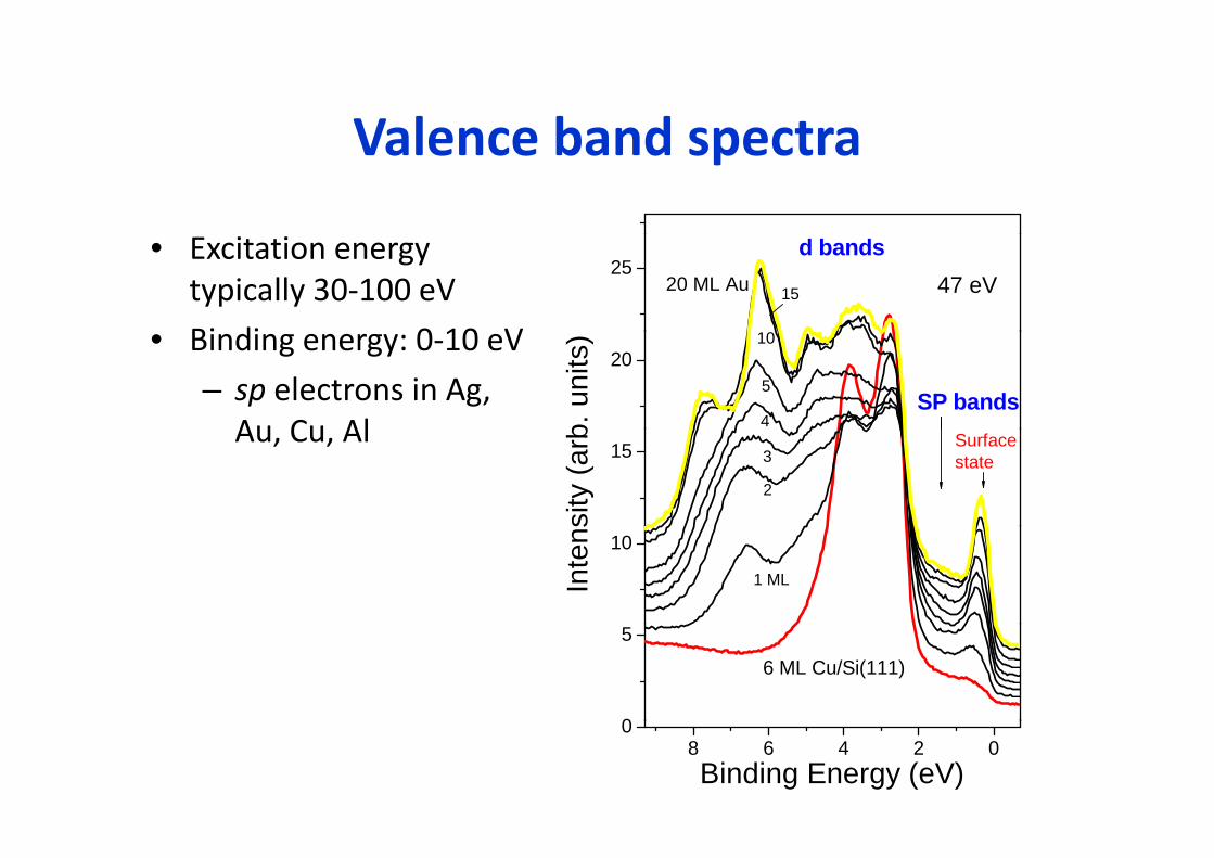
Valence band spectraValence band spectra
• Excitation energy typically 30‐100 eV
Bi di 0 10 V
2520 ML Au 15
10
d bands47 eV
• Binding energy: 0‐10 eV
– sp electrons in Ag, Au Cu Al
2010
5
4b. u
nits
)
SP bandsAu, Cu, Al
15 3
2
sity
(arb Surface
state
10
1 MLInte
ns
0
5
6 ML Cu/Si(111)
8 6 4 2 00
Binding Energy (eV)
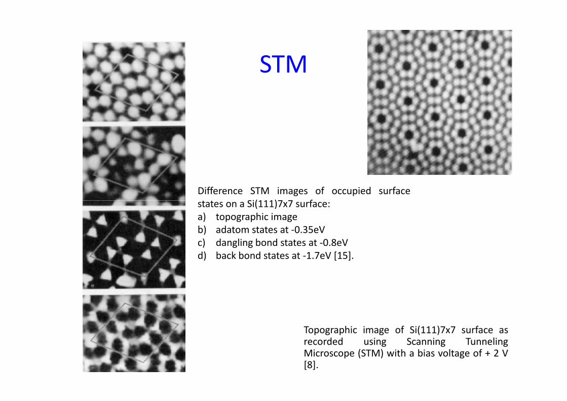
STMSTM
Difference STM images of occupied surfaceSi(111)7 7 fstates on a Si(111)7x7 surface:
a) topographic imageb) adatom states at ‐0.35eVc) dangling bond states at ‐0.8eV) g gd) back bond states at ‐1.7eV [15].
Topographic image of Si(111)7x7 surface asrecorded using Scanning TunnelingMicroscope (STM) with a bias voltage of + 2 V[8].
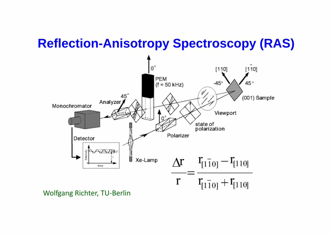
Reflection-Anisotropy Spectroscopy (RAS)
Wolfgang Richter, TU‐Berlin
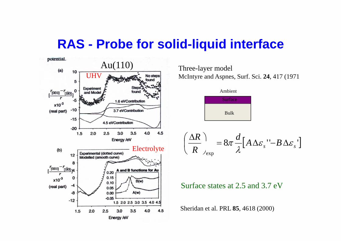
RAS - Probe for solid-liquid interfaceAu(110) Th l d l
UHVAu(110) Three-layer model
McIntyre and Aspnes, Surf. Sci. 24, 417 (1971
Ambient
Surface
Bulk
Electrolyte[ ]'''8 ss BAd
RR εε
λπ Δ−Δ=⎟
⎠⎞
⎜⎝⎛ Δ
Electrolyte[ ]
expssR λ⎠⎝
Surface states at 2.5 and 3.7 eV
Sheridan et al. PRL 85, 4618 (2000)
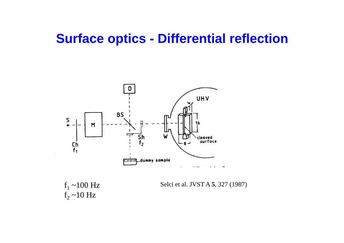
Surface optics - Differential reflectionSurface optics - Differential reflection
f1 ~100 Hzf2 ~10 Hz
Selci et al. JVST A 5, 327 (1987)
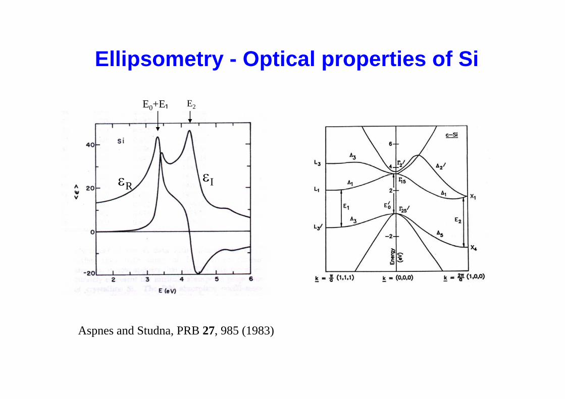
Ellipsometry - Optical properties of SiEllipsometry Optical properties of Si
E0+E₁ E20
εIεR
Aspnes and Studna, PRB 27, 985 (1983)p , , ( )

Depth sensitivity of linear optics
The probe depth can bevaried through the wavelength
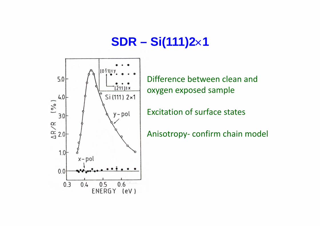
SDR – Si(111)2×1
Difference between clean and d loxygen exposed sample
Excitation of surface statesExcitation of surface states
Anisotropy‐ confirm chain model
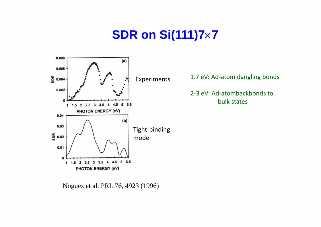
SDR on Si(111)7×7SDR on Si(111)7×7
Experiments 1.7 eV: Ad‐atom dangling bonds
2‐3 eV: Ad‐atombackbonds to bulk states
Tight‐bindingmodelmodel
Noguez et al. PRL 76, 4923 (1996)