Embed Size (px)
Citation preview
7/27/2019 Lecture6(20-3-11)
http://slidepdf.com/reader/full/lecture620-3-11 1/6
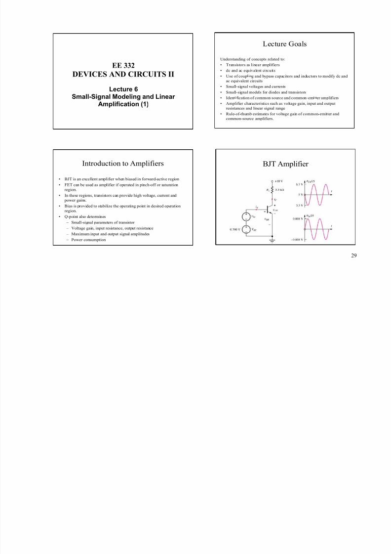
EE 332
DEVICES AND CIRCUITS II
Lecture 6
Small-Signal Modeling and Linear Amplification (1)
Introduction to Amplifiers
• BJT is an excellent amplifier when biased in forward-active region
• FET can be used as amplifier if operated in pinch-off or saturation
region.
• In these regions, transistors can provide high voltage, current and
power gains.
• Bias is provided to stabilize the operating point in desired operation
region.
• Q-point also determines
– Small-signal parameters of transistor
– Voltage gain, input resistance, output resistance
– Maximum input and output signal amplitudes
– Power consumption
BJT Amplifier
Lecture Goals
Understanding of concepts related to:
• Transistors as linear amplifiers
• dc and ac equivalent circuits
• Use of coupling and bypass capacitors and inductors to modify dc and
ac equivalent circuits
• Small-signal voltages and currents
• Small-signal models for diodes and transistors
• Identification of common-source and common-emitter amplifiers
• Amplifier characteristics such as voltage gain, input and output
resistances and linear signal range
• Rule-of-thumb estimates for voltage gain of common-emitter and
common-source amplifiers.
29
7/27/2019 Lecture6(20-3-11)
http://slidepdf.com/reader/full/lecture620-3-11 2/6
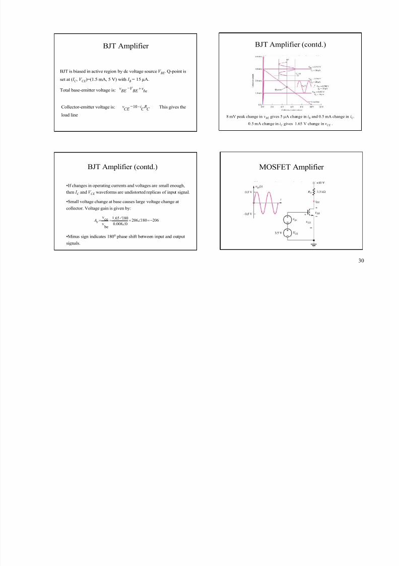
BJT Amplifier
BJT is biased in active region by dc voltage source V BE . Q-point is
set at ( I C , V CE )=(1.5 mA, 5 V) with I B = 15 μA.
Total base-emitter voltage is: bev
BE V
BE v +=
Collector-emitter voltage is: This gives the
load line
C RC i
CE v −=10
BJT Amplifier (contd.)
•If changes in operating currents and voltages are small enough,
then I C and V CE waveforms are undistorted replicas of input signal.
•Small voltage change at base causes large voltage change at
collector. Voltage gain is given by:
•Minus sign indicates 1800 phase shift between input and output
signals.
2061802060008.0
18065.1
bev
cev−=∠=
∠
∠==v A
MOSFET Amplifier
BJT Amplifier (contd.)
8 mV peak change in v BE gives 5 μA change in i B and 0.5 mA change in iC .
0.5 mA change in iC gives 1.65 V change in vCE .
30
7/27/2019 Lecture6(20-3-11)
http://slidepdf.com/reader/full/lecture620-3-11 3/6
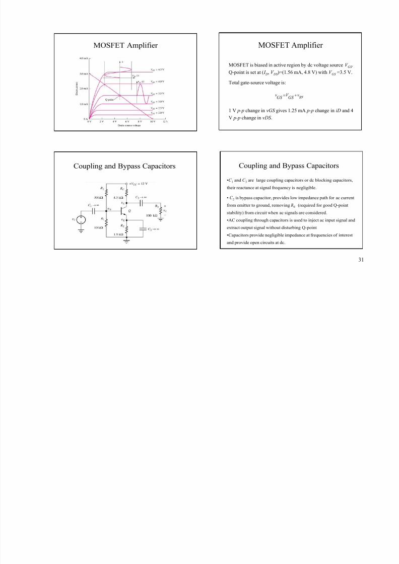
MOSFET Amplifier
Coupling and Bypass Capacitors
Coupling and Bypass Capacitors
•C 1 and C 3 are large coupling capacitors or dc blocking capacitors,
their reactance at signal frequency is negligible.
• C 2 is bypass capacitor, provides low impedance path for ac current
from emitter to ground, removing RE (required for good Q-point
stability) from circuit when ac signals are considered.
•AC coupling through capacitors is used to inject ac input signal and
extract output signal without disturbing Q-point
•Capacitors provide negligible impedance at frequencies of interest
and provide open circuits at dc.
MOSFET Amplifier
MOSFET is biased in active region by dc voltage source V GS .
Q-point is set at ( I D, V DS )=(1.56 mA, 4.8 V) with V GS =3.5 V.
Total gate-source voltage is:
1 V p-p change in vGS gives 1.25 mA p-p change in iD and 4
V p-p change in vDS .
gsv
GS V
GS v +=
31
7/27/2019 Lecture6(20-3-11)
http://slidepdf.com/reader/full/lecture620-3-11 4/6
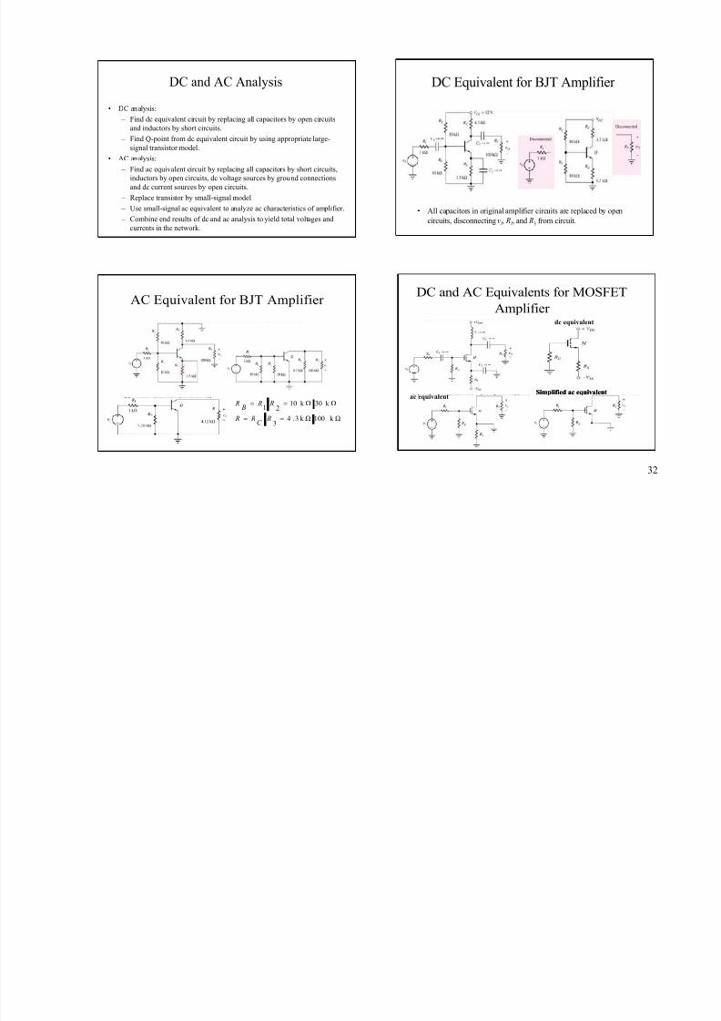
DC and AC Analysis
• DC analysis:
– Find dc equivalent circuit by replacing all capacitors by open circuits
and inductors by short circuits.
– Find Q-point from dc equivalent circuit by using appropriate large-
signal transistor model.
• AC analysis:
– Find ac equivalent circuit by replacing all capacitors by short circuits,
inductors by open circuits, dc voltage sources by ground connectionsand dc current sources by open circuits.
– Replace transistor by small-signal model
– Use small-signal ac equivalent to analyze ac characteristics of amplifier.
– Combine end results of dc and ac analysis to yield total voltages and
currents in the network.
AC Equivalent for BJT Amplifier
k Ω100k Ω3.43
k Ω30k Ω1021
==
==
RC
R R
R R B
R
DC and AC Equivalents for MOSFET
Amplifier dc equivalent
ac equivalentSimplified ac equivalentSimplified ac equivalent
DC Equivalent for BJT Amplifier
• All capacitors in original amplifier circuits are replaced by open
circuits, disconnecting v I , R
I , and R3 from circuit.
32
7/27/2019 Lecture6(20-3-11)
http://slidepdf.com/reader/full/lecture620-3-11 5/6
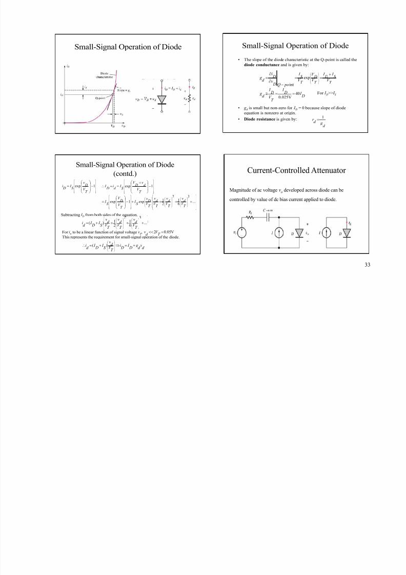
Small-Signal Operation of Diode
Small-Signal Operation of Diode
(contd.)
⎥⎥⎥⎥
⎥
⎦
⎤
⎢⎢⎢⎢
⎢
⎣
⎡
⎟⎟⎟
⎠
⎞
⎜⎜⎜
⎝
⎛
⎟⎟⎟
⎠
⎞
⎜⎜⎜
⎝
⎛
⎟⎟⎟
⎠
⎞
⎜⎜⎜
⎝
⎛
⎥⎥⎥⎥
⎥
⎦
⎤
⎢⎢⎢⎢
⎢
⎣
⎡
⎥⎥⎥⎥⎥
⎦
⎤
⎢⎢⎢⎢⎢
⎣
⎡
++++−⎟⎟ ⎠
⎞
⎜⎜⎝
⎛
=
−⎟⎟
⎠
⎞
⎜⎜
⎝
⎛ +=+∴
...
3
61
2
21exp1exp
1exp
T V d v
T V d v
T V d v
T V Dv
S I
T V DV
S I
T V
d v
DV
S I
d i
D I
⎥⎥⎥⎥⎥
⎦
⎤
⎢⎢⎢⎢⎢
⎣
⎡
−⎟⎟
⎠
⎞
⎜⎜
⎝
⎛ = 1exp
T V Dv
S I
Di
Subtracting I D from both sides of the equation,
⎥⎥⎥⎥⎥
⎦
⎤
⎢⎢⎢⎢⎢
⎣
⎡
⎟⎟⎟
⎠
⎞
⎜⎜⎜
⎝
⎛
⎟⎟⎟
⎠
⎞
⎜⎜⎜
⎝
⎛
++++= ...
3
61
2
21)(
T V d v
T V d v
T V d v
S I
D I
d i
For id to be a linear function of signal voltage vd ,
This represents the requirement for small-signal operation of the diode.
V05.02 =<<T
V d v
d v
d g
D I
Di
T V d v
S I
D I
d i +=⇒+=
⎟⎟⎟
⎠
⎜⎜⎜
⎝
)( ⎞⎛
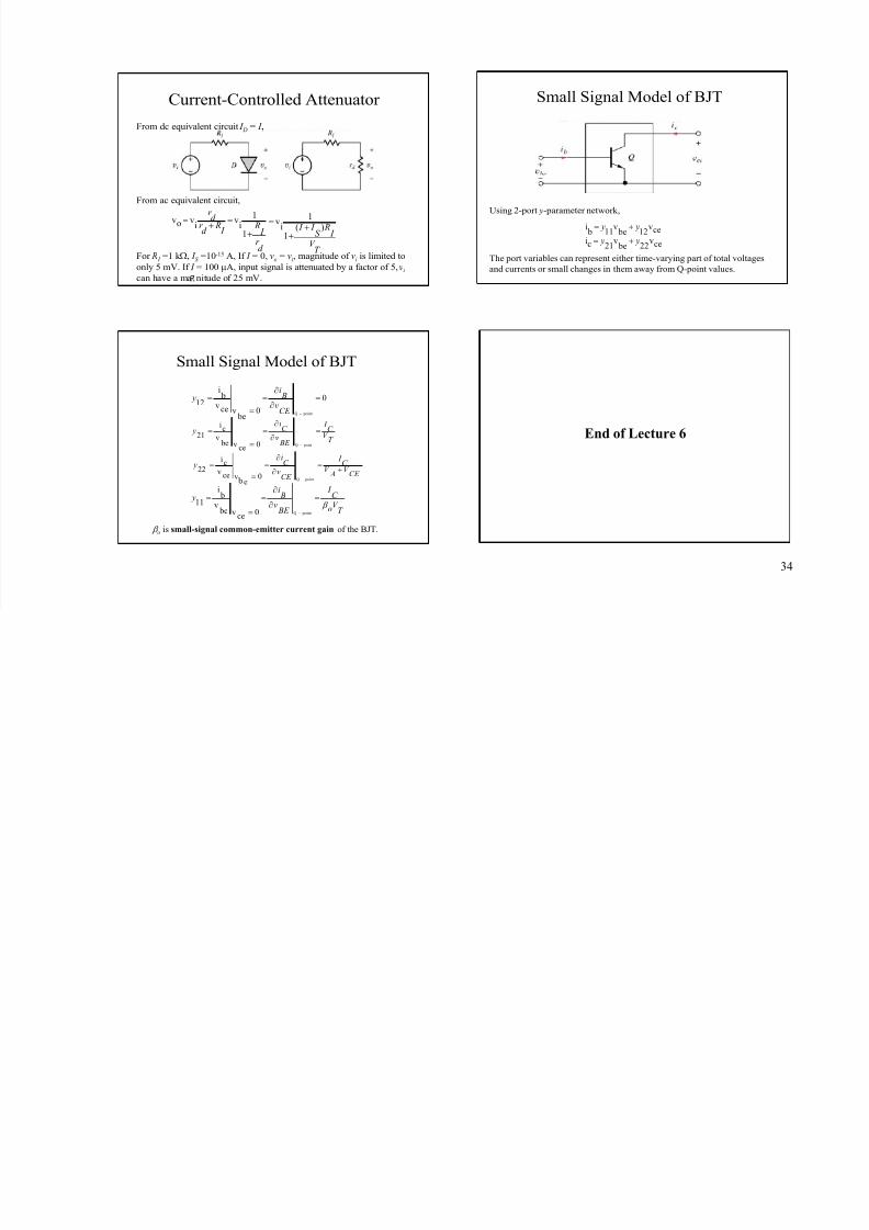
Current-Controlled Attenuator
Magnitude of ac voltage vo
developed across diode can be
controlled by value of dc bias current applied to diode.
Small-Signal Operation of Diode
• The slope of the diode characteristic at the Q-point is called the
diode conductance and is given by:
• g d is small but non-zero for I D = 0 because slope of diode
equation is nonzero at origin.
• Diode resistance is given by:
D I D
I
T V D I
d g
T V
S I
D I
T V DV
T V S
I
poQ Dv Di
d g
40V025.0
exp
int
==≅
+==
−∂
∂=
⎟⎟⎟
⎠
⎞
⎜⎜⎜
⎝
⎛
For I D>> I S
d g d
r 1
=
∴
33
7/27/2019 Lecture6(20-3-11)
http://slidepdf.com/reader/full/lecture620-3-11 6/6