Embed Size (px)
Citation preview

NNaannoommaakkeerr Lab$#4:$Organic$Light$Emi2ng$Diode$(OLED)$$
1
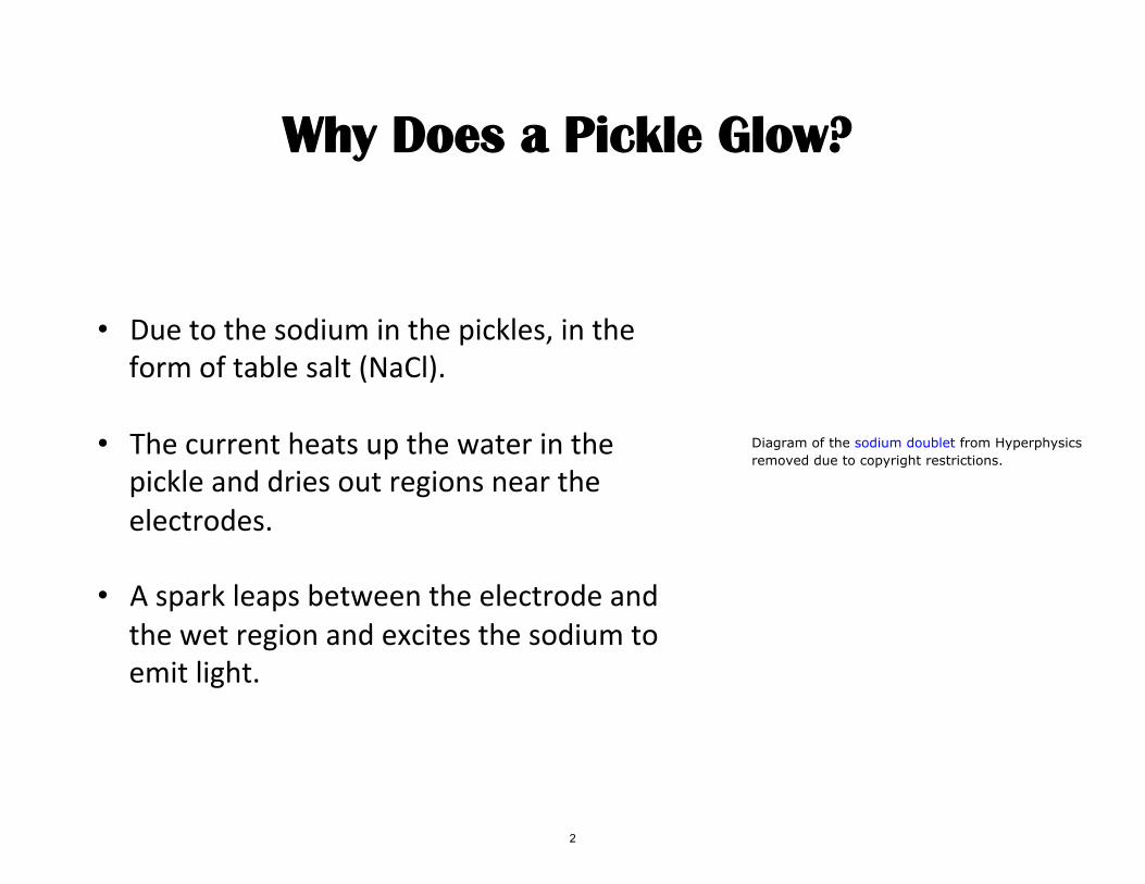
WWhhyy DDooeess aa PPiicckkllee GGllooww??
• Due$to$the$sodium$in$the$pickles,$in$the$ form$of$table$salt$(NaCl).$
• The$current$heats$up$the$water$in$the$ pickle$and$dries$out$regions$near$the$ electrodes.$
• A$spark$leaps$between$the$electrode$and$ the$wet$region$and$excites$the$sodium$to$ emit$light.$
2
Diagram of the sodium doublet from Hyperphysicsremoved due to copyright restrictions.
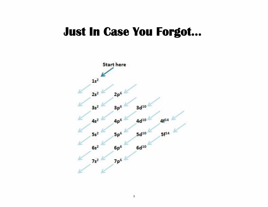
JJuusstt IInn CCaassee YYoouu FFoorrggoott……
3
OOrrggaanniicc LLEEDD DDiissppllaayy CChhaarrggee TTrraannssppoorrtt LLaayyeerr
FFaabbrriiccaattiioonn
4
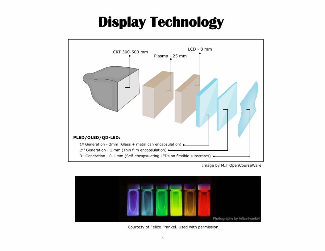
DDiissppllaayy TTeecchhnnoollooggyy
Courtesy of Felice Frankel. Used with permission.
5
CRT 300-500 mmPlasma - 25 mm
LCD - 8 mm
PLED/OLED/QD-LED:
1st Generation - 2mm (Glass + metal can encapsulation)2nd Generation - 1 mm (Thin film encapsulation)3rd Generation - 0.1 mm (Self-encapsulating LEDs on flexible substrates)
Image by MIT OpenCourseWare.
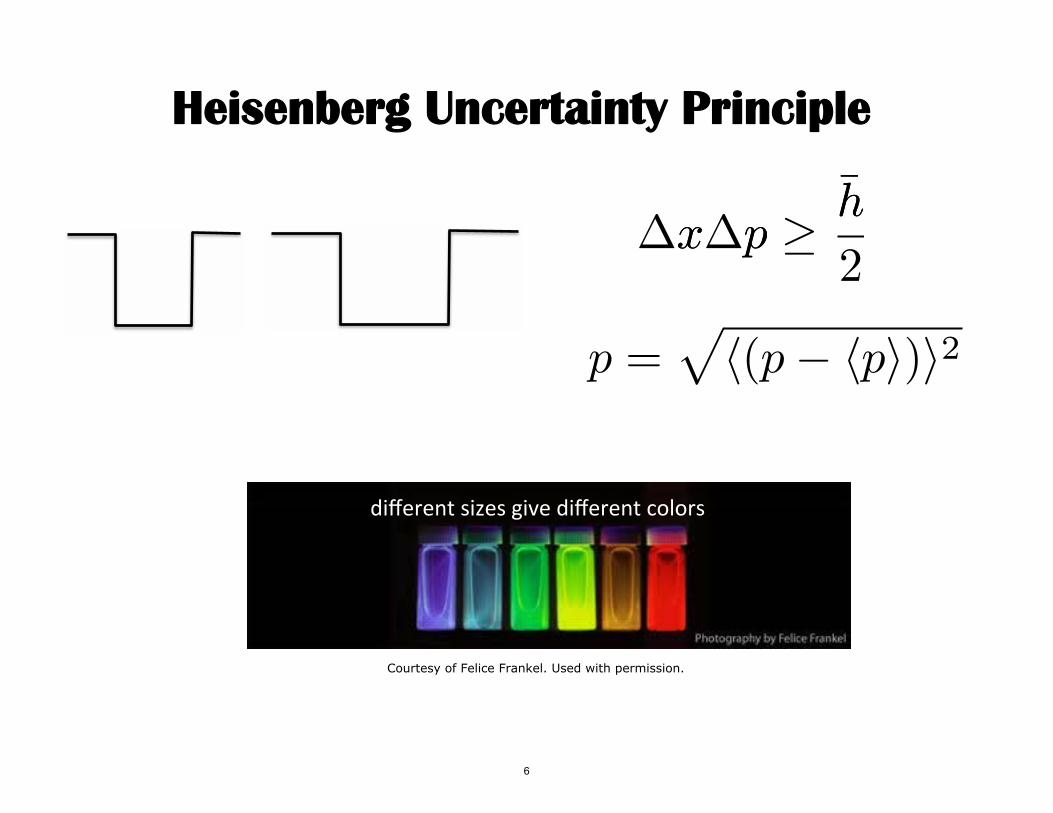
HHeeiisseennbbeerrgg UUnncceerrttaaiinnttyy PPrriinncciippllee
h̄
x p
2 2
p = ph(p − hpi)i
different$sizes$give$different$colors$
Courtesy of Felice Frankel. Used with permission.
6
�x�p � h̄
OOrrggaanniicc LLEEDD DDiissppllaayy CChhaarrggee TTrraannssppoorrtt LLaayyeerr
FFaabbrriiccaattiioonn
7
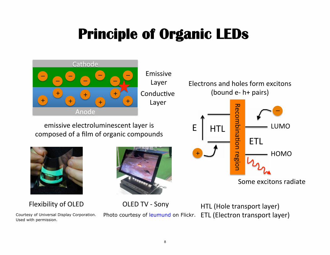
Emissive$ Layer$
ConducGve$ Layer$
Electrons$and$holes$form$excitons$ (bound$eK$h+$pairs)$
emissive$electroluminescent$layer$is$ composed$of$a$film$of$organic$compounds$
E$ ETL$
LUMO$
HOMO$
Some$excitons$radiate$
Flexibility$of$OLED$ OLED$TV$K$Sony$ HTL$(Hole$transport$layer)$
Cathode$ �$
�$
�$ �$ �$ �$ �$ �$
�$ �$ �$ �$ �$ �$ RecombinaGon$region$
�$
�$
HTL$
PPrriinncciippllee ooff OOrrggaanniicc LLEEDDss
Anode$
3KRWR�FRXUWHV\�RI�OHXPXQG�RQ�)OLFNU� ETL$(Electron$transport$layer)$ Courtesy of Universal Display Corporation.Used with permission.
8
OOrrggaanniicc LLEEDDss
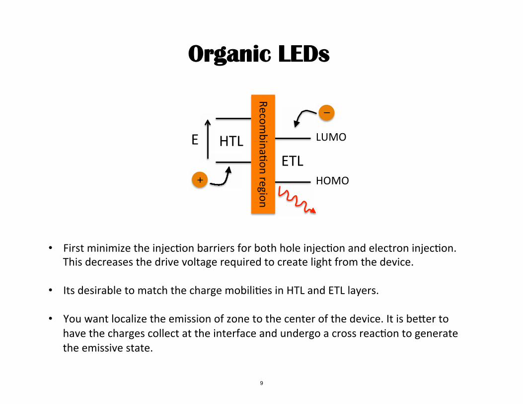
RecombinaGon$region$
LUMO$
HOMO$
�$
�$ ETL$
HTL$E$
• First$minimize$the$injecGon$barriers$for$both$hole$injecGon$and$electron$injecGon.$ This$decreases$the$drive$voltage$required$to$create$light$from$the$device.$
• Its$desirable$to$match$the$charge$mobiliGes$in$HTL$and$ETL$layers.$$
• You$want$localize$the$emission$of$zone$to$the$center$of$the$device.$It$is$beVer$to$ have$the$charges$collect$at$the$interface$and$undergo$a$cross$reacGon$to$generate$ the$emissive$state.$
9
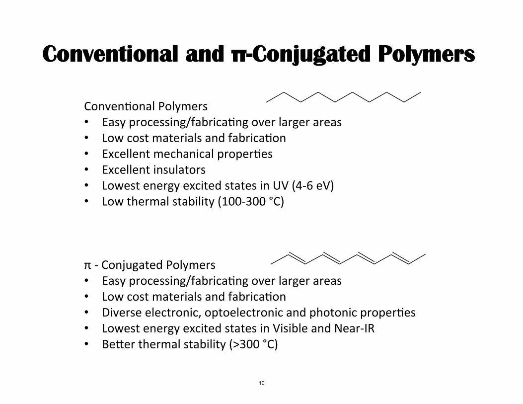
CCoonnvveennttiioonnaall aanndd ππ--CCoonnjjuuggaatteedd PPoollyymmeerrss
ConvenGonal$Polymers$ • Easy$processing/fabricaGng$over$larger$areas$ • Low$cost$materials$and$fabricaGon$ • Excellent$mechanical$properGes$ • Excellent$insulators$ • Lowest$energy$excited$states$in$UV$(4K6$eV)$ • Low$thermal$stability$(100K300$°C)$
π$K$Conjugated$Polymers$ • Easy$processing/fabricaGng$over$larger$areas$ • Low$cost$materials$and$fabricaGon$ • Diverse$electronic,$optoelectronic$and$photonic$properGes$ • Lowest$energy$excited$states$in$Visible$and$NearKIR$ • BeVer$thermal$stability$(>300$°C)$
10
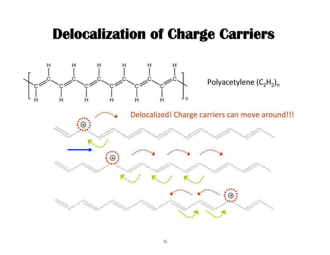
DDeellooccaalliizzaattiioonn ooff CChhaarrggee CCaarrrriieerrss
Delocalized!$Charge$carriers$can$move$around!!!$
Polyacetylene$(C2H2)n$
11
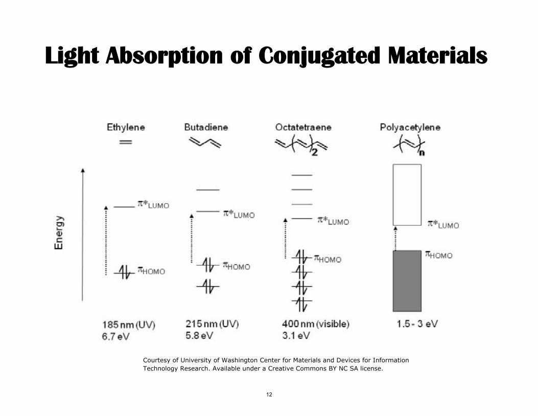
LLiigghhtt AAbbssoorrppttiioonn ooff CCoonnjjuuggaatteedd MMaatteerriiaallss
Courtesy of University of Washington Center for Materials and Devices for InformationTechnology Research. Available under a Creative Commons BY NC SA license.
12
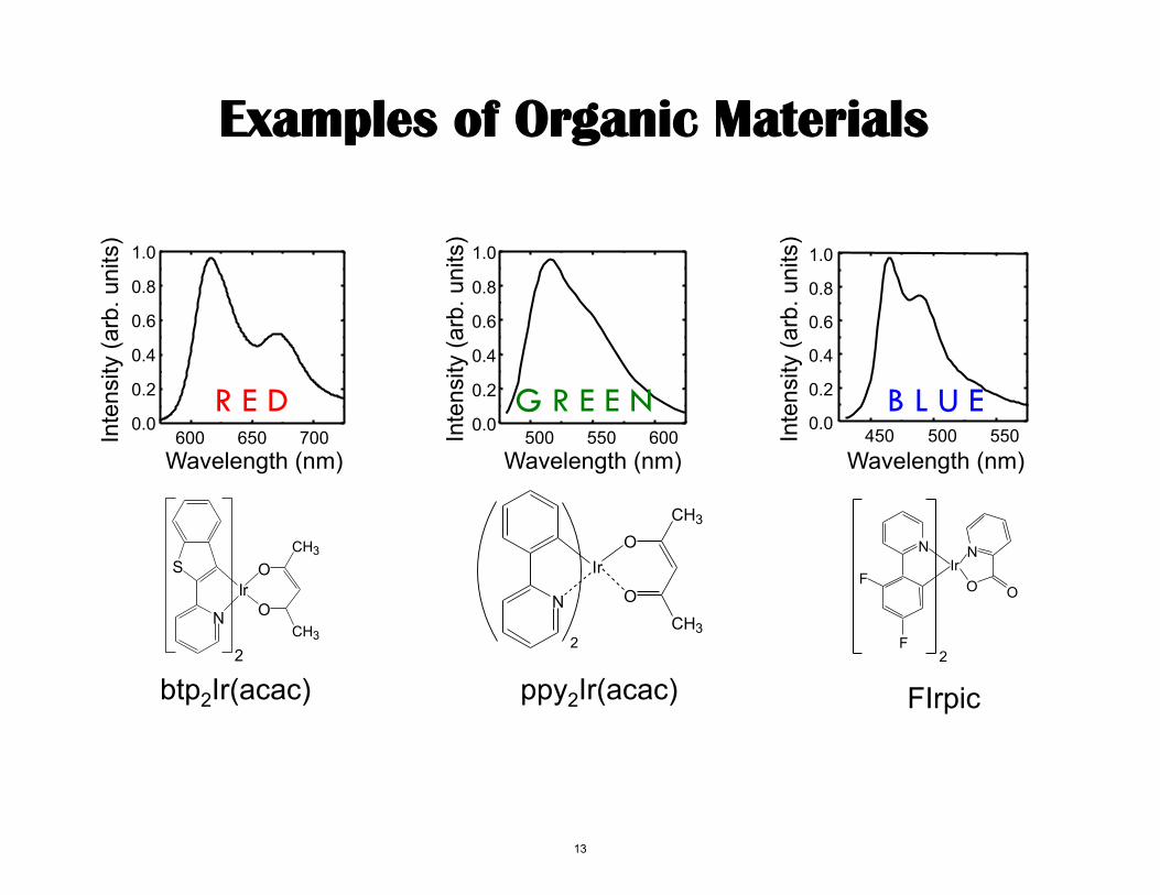
EExxaammpplleess ooff OOrrggaanniicc MMaatteerriiaallss In
tens
ity (a
rb. u
nits
)
Inte
nsity
(arb
. uni
ts)
1.0
0.8
0.6
0.4
0.2
0.0 G R E E N
500 550 600 Inte
nsity
(arb
. uni
ts)
1.0
0.8
0.6
0.4
0.2
0.0 B L U E
450 500 550
1.0
0.8
0.6
0.4
0.2
0.0 R E D
600 650 700 Wavelength (nm) Wavelength (nm) Wavelength (nm)
S
N
CH3
Ir
2
N O
2
OCH3 N N IrIrO
OF O
O CH3CH3 F
2
btp2Ir(acac) ppy2Ir(acac) FIrpic
13
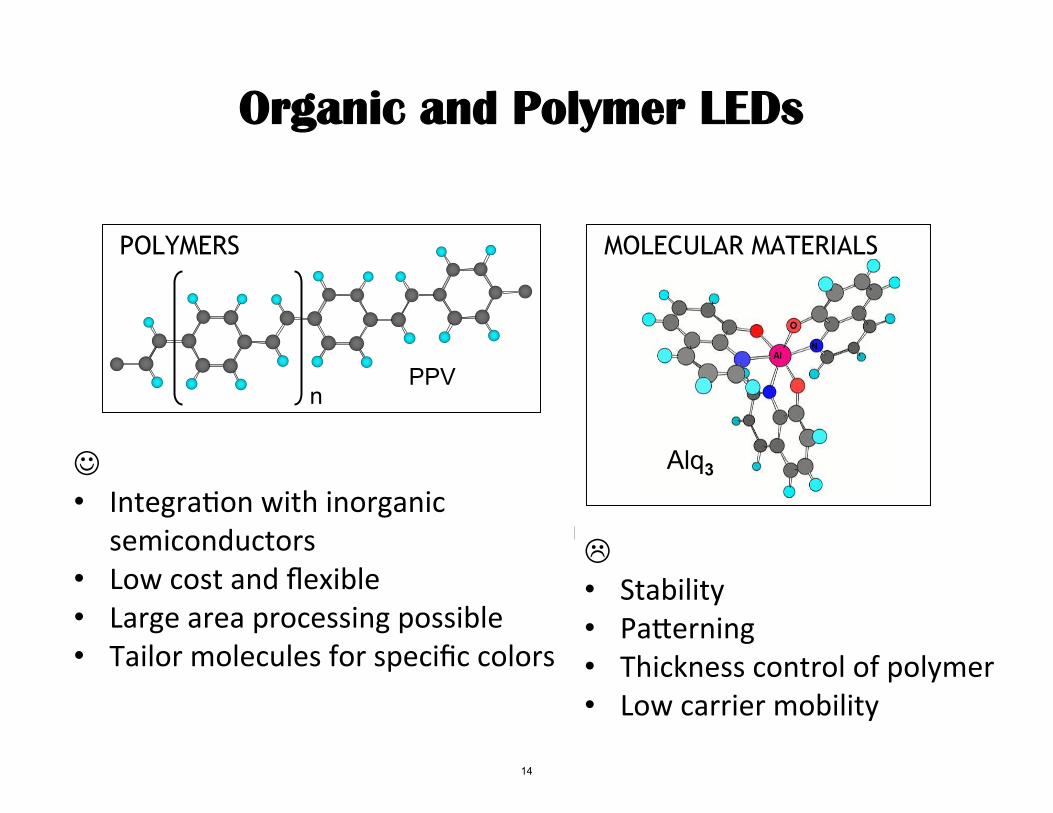
OOrrggaanniicc aanndd PPoollyymmeerr LLEEDDss
Alq3
MOLECULAR MATERIALS
PPV
POLYMERS
n
$ Attractive due to:Attractive due to:
99 Integrability with inorganic semiconductors
99 Low cost (fabric dyes, biologically derived materials)
99 Large area bulk processing possible
99 Tailor molecules for specific electronic or optical properties
99 Unusual properties not easily attainablewith conventional materials
But problems exist:But problems exist:
99 Stability
99 Patterning
99 Thickness control of polymers
99 Low carrier mobility
J • IntegraGon with inorganic
semiconductors • Low cost and flexible • Large area processing possible • Tailor molecules for specific colors
L • Stability • PaVerning • Thickness control of polymer • Low carrier mobility
14
Cathode$
Anode$
�$
�$
�$ �$ �$ �$ �$ �$
�$ �$ �$ �$ �$ �$
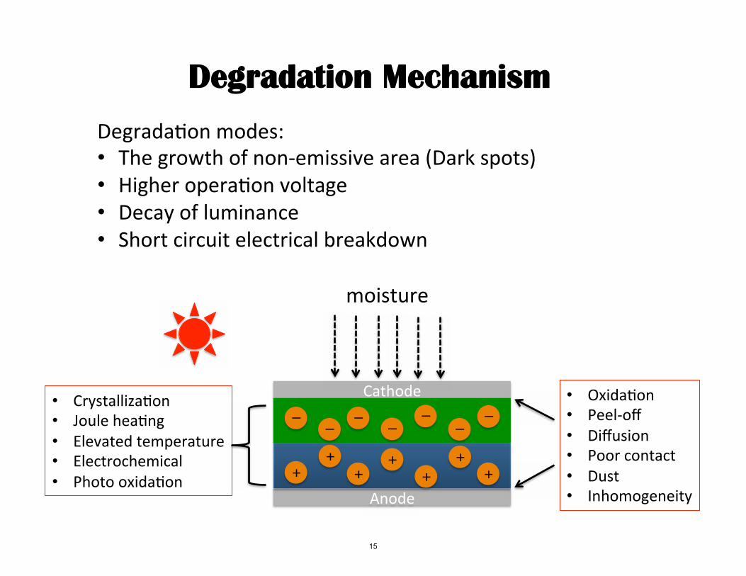
DDeeggrraaddaattiioonn MMeecchhaanniissmm DegradaGon$modes:$ • The$growth$of$nonKemissive$area$(Dark$spots)$ • Higher$operaGon$voltage$ • Decay$of$luminance$ • Short$circuit$electrical$breakdown$
moisture$
• CrystallizaGon$ • Joule$heaGng$ • Elevated$temperature$ • Electrochemical$ • Photo$oxidaGon$
• OxidaGon$ • PeelKoff$ • Diffusion$ • Poor$contact$ • Dust$ • Inhomogeneity$
15
OOrrggaanniicc LLEEDD DDiissppllaayy CChhaarrggee TTrraannssppoorrtt LLaayyeerr
FFaabbrriiccaattiioonn
16
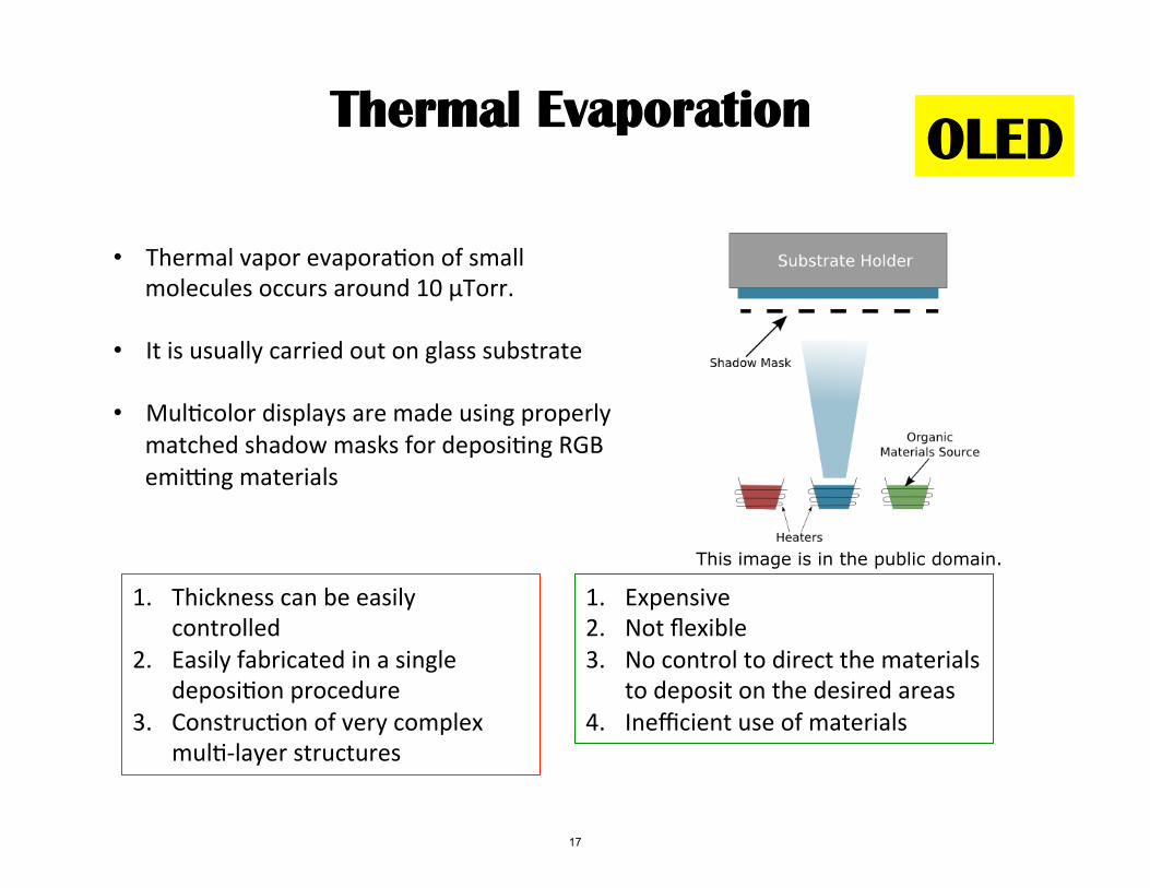
TThheerrmmaall EEvvaappoorraattiioonn OOLLEEDD
• Thermal$vapor$evaporaGon$of$small$ molecules$occurs$around$10$μTorr.$
• It$is$usually$carried$out$on$glass$substrate$
• MulGcolor$displays$are$made$using$properly$ matched$shadow$masks$for$deposiGng$RGB$ emiing$materials$
1. Thickness$can$be$easily$ 1. controlled$ 2.
2. Easily$fabricated$in$a$single$ 3. deposiGon$procedure$
3. ConstrucGon$of$very$complex$ 4. mulGKlayer$structures$
7KLV�LPDJH�LV�LQ�WKH�SXEOLF�GRPDLQ�
Expensive$ Not$flexible$ No$control$to$direct$the$materials$ to$deposit$on$the$desired$areas$ Inefficient$use$of$materials$
17

TThheerrmmaall EEvvaappoorraattoorr
Load Lock
Ante Chamber and Oven
Sputtering
M ITO M ceramics
Evaporative Deposition
M molecular organics (amorphous and crystalline)
M metals
Source Storage SHADOW MASK
STORAGE-EXCANGE
SIX THERMALLY HEATED SOURCES TWO INDEPENDENT BANKS of THREE SOURCES EACH
E-BEAM EVAPORATION SINGLE POCKET
INDEPENDENT SOURCE MONITORING
DURING CO-DEPOSITION
18
3KRWRJUDSK�RI�VSLQQHU�UHPRYHG GXH�WR�FRS\ULJKW�UHVWULFWLRQV�
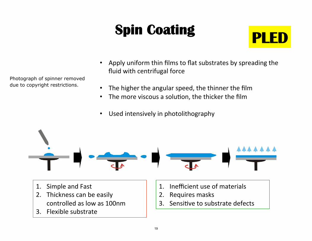
SSppiinn CCooaattiinngg PPLLEEDD • Apply$uniform$thin$films$to$flat$substrates$by$spreading$the$
fluid$with$centrifugal$force$
• The$higher$the$angular$speed,$the$thinner$the$film$ • The$more$viscous$a$soluGon,$the$thicker$the$film$
• Used$intensively$in$photolithography$
1. Simple$and$Fast$ 2. Thickness$can$be$easily$
controlled$as$low$as$100nm$ 3. Flexible$substrate$
1. Inefficient$use$of$materials$ 2. Requires$masks$ 3. SensiGve$to$substrate$defects$
19
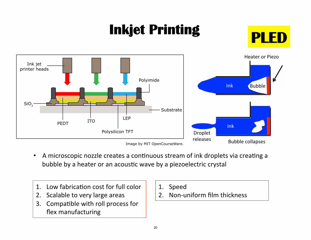
IInnkkjjeett PPrriinnttiinngg PPLLEEDD Heater$or$Piezo$
$
Ink$ Bubble$
Droplet$ releases$ Bubble$collapses$
Ink$
• A$microscopic$nozzle$creates$a$conGnuous$stream$of$ink$droplets$via$creaGng$a$ bubble$by$a$heater$or$an$acousGc$wave$by$a$piezoelectric$crystal$
1. Low$fabricaGon$cost$for$full$color$ 1. Speed$ 2. Scalable$to$very$large$areas$ 2. NonKuniform$film$thickness$ 3. CompaGble$with$roll$process$for$
flex$manufacturing$
20
Polyimide
Substrate
Polysilicon TFT
LEPPEDT
SiO2
ITO
Ink jet printer heads
Image by MIT OpenCourseWare.
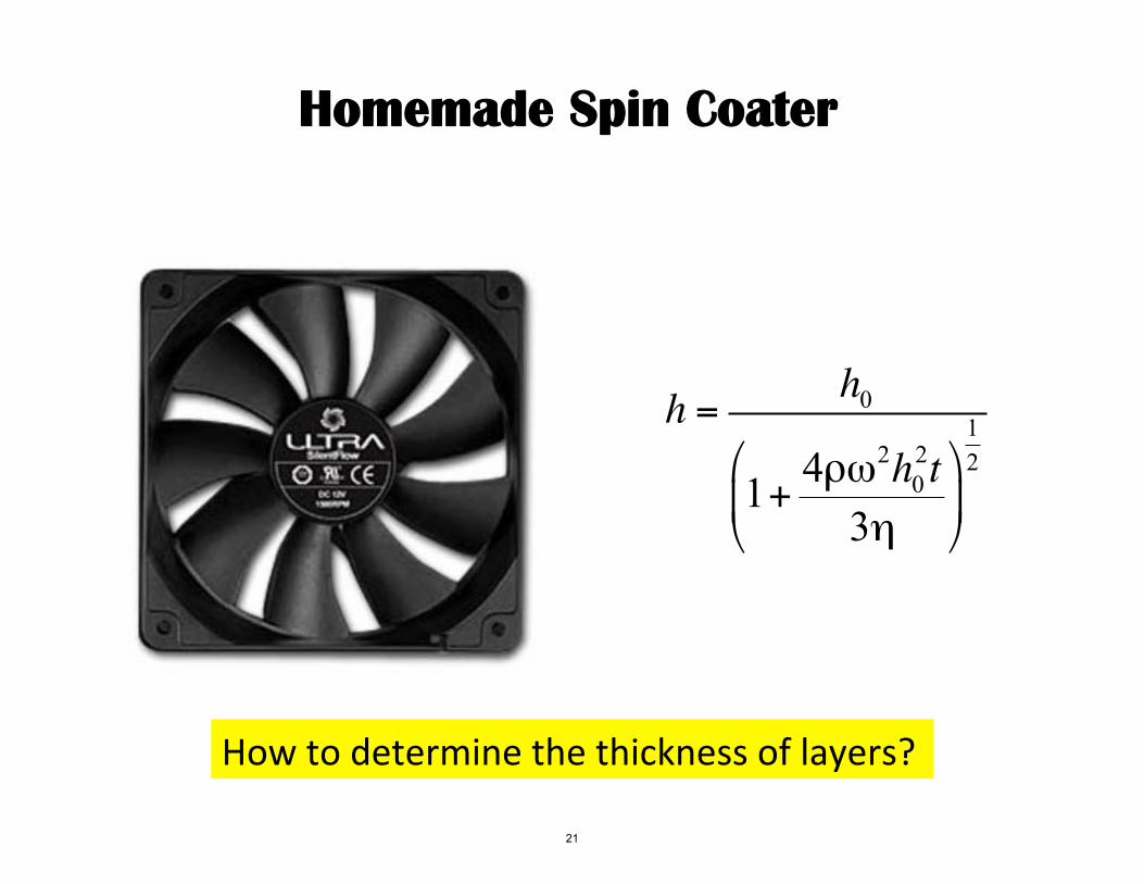
HHoommeemmaaddee SSppiinn CCooaatteerr
h0h = 1 $ 4ρω2h0
2t '2
&1+ )% 3η (
How$to$determine$the$thickness$of$layers?$
21
CCoonncclluussiioonnss
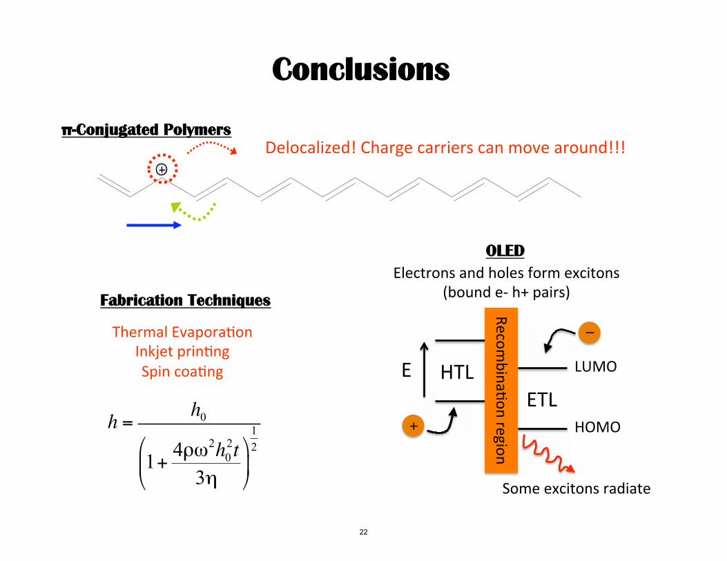
Delocalized!$Charge$carriers$can$move$around!!!$ ππ--CCoonnjjuuggaatteedd PPoollyymmeerrss$
OOLLEEDD$ Electrons$and$holes$form$excitons$
(bound$eK$h+$pairs)$ FFaabbrriiccaattiioonn TTeecchhnniiqquueess$
Thermal$EvaporaGon$ Inkjet$prinGng$ Spin$coaGng$
h0h = 1 $ 4ρω2h0
2t '2
&1+ )% 3η ( Some$excitons$radiate$
RecombinaGon$region$
LUMO$
HOMO$
�$
�$ ETL$
HTL$E$
22

MIT OpenCourseWarehttp://ocw.mit.edu
6.S079 NanomakerSpring 2013 For information about citing these materials or our Terms of Use, visit: http://ocw.mit.edu/terms.