Embed Size (px)
Citation preview
Extracted from Agrawal & Bushnell VLSI Test: Lecture 15 1
Memory complexity
Memory fault models
March test algorithms
Summary
Lecture on
Memory Test
Importance of memories
0%
10%
20%
30%
40%
50%
60%
70%
80%
90%
100%
99 02 05 08 11 14
Memory Logic-Reused Logic-New
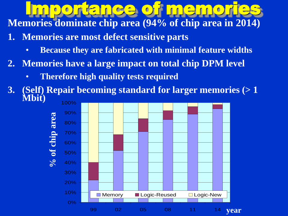
Memories dominate chip area (94% of chip area in 2014)
1. Memories are most defect sensitive parts
• Because they are fabricated with minimal feature widths
2. Memories have a large impact on total chip DPM level
• Therefore high quality tests required
3. (Self) Repair becoming standard for larger memories (> 1 Mbit)
% o
f ch
ip a
rea
year
Extracted from Agrawal & Bushnell VLSI Test: Lecture 15 3
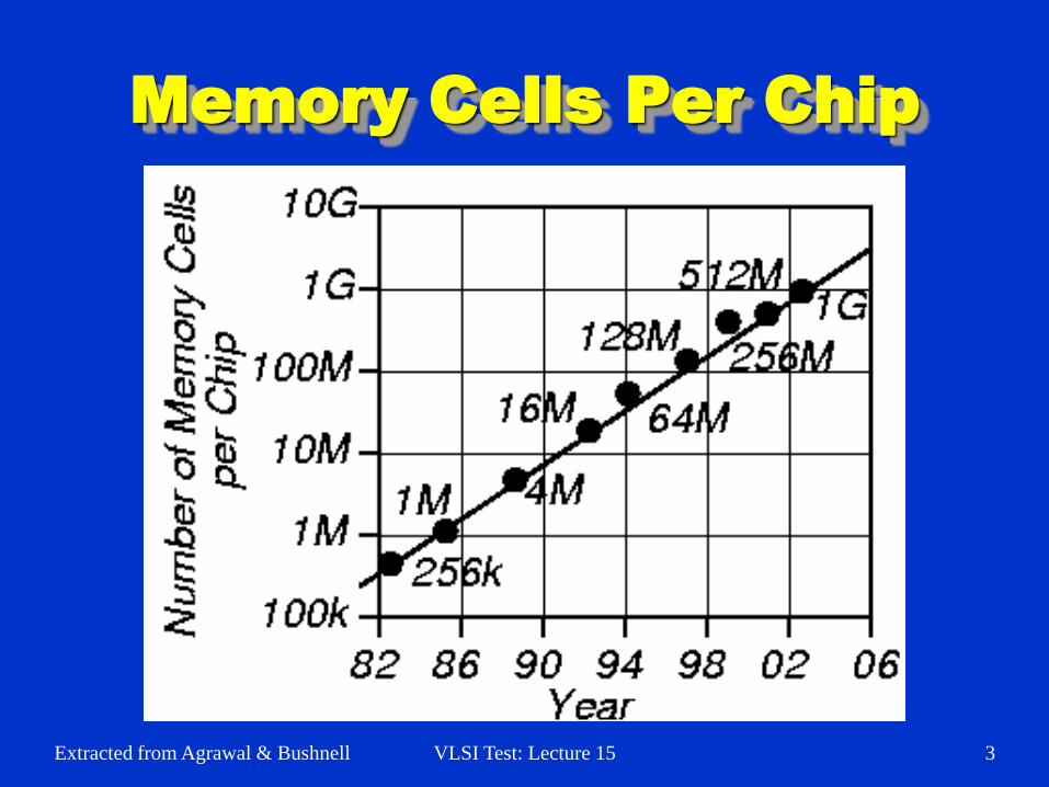
Memory Cells Per Chip
Extracted from Agrawal & Bushnell VLSI Test: Lecture 15 4
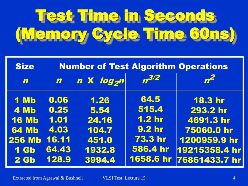
Test Time in Seconds
(Memory Cycle Time 60ns)
n
1 Mb
4 Mb
16 Mb
64 Mb
256 Mb
1 Gb
2 Gb
n
0.06
0.25
1.01
4.03
16.11
64.43
128.9
n X log2n
1.26
5.54
24.16
104.7
451.0
1932.8
3994.4
n3/2
64.5
515.4
1.2 hr
9.2 hr
73.3 hr
586.4 hr
1658.6 hr
n2
18.3 hr
293.2 hr
4691.3 hr
75060.0 hr
1200959.9 hr
19215358.4 hr
76861433.7 hr
Size Number of Test Algorithm Operations

Extracted from Agrawal & Bushnell VLSI Test: Lecture 15 5
Functional Model
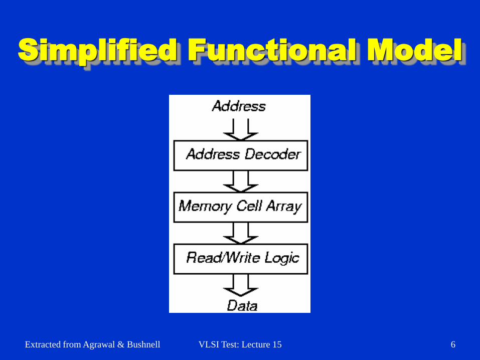
Extracted from Agrawal & Bushnell VLSI Test: Lecture 15 6
Simplified Functional Model
Extracted from Agrawal & Bushnell VLSI Test: Lecture 15 7
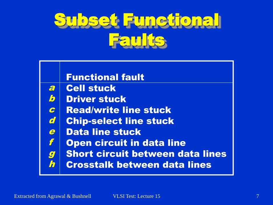
Subset Functional
Faults
a
b
c
d
e
f
g
h
Functional fault
Cell stuck
Driver stuck
Read/write line stuck
Chip-select line stuck
Data line stuck
Open circuit in data line
Short circuit between data lines
Crosstalk between data lines
Extracted from Agrawal & Bushnell VLSI Test: Lecture 15 8
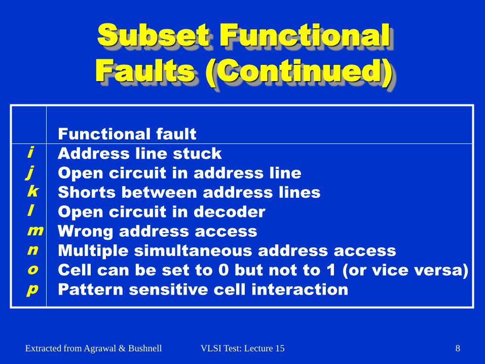
Subset Functional
Faults (Continued)
i
j
k
l
m
n
o
p
Functional fault
Address line stuck
Open circuit in address line
Shorts between address lines
Open circuit in decoder
Wrong address access
Multiple simultaneous address access
Cell can be set to 0 but not to 1 (or vice versa)
Pattern sensitive cell interaction
Extracted from Agrawal & Bushnell VLSI Test: Lecture 15 9
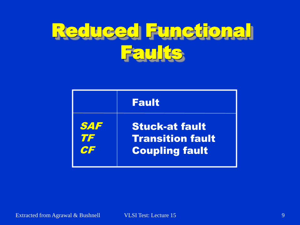
Reduced Functional
Faults
SAF
TF
CF
Fault
Stuck-at fault
Transition fault
Coupling fault
Extracted from Agrawal & Bushnell VLSI Test: Lecture 15 10
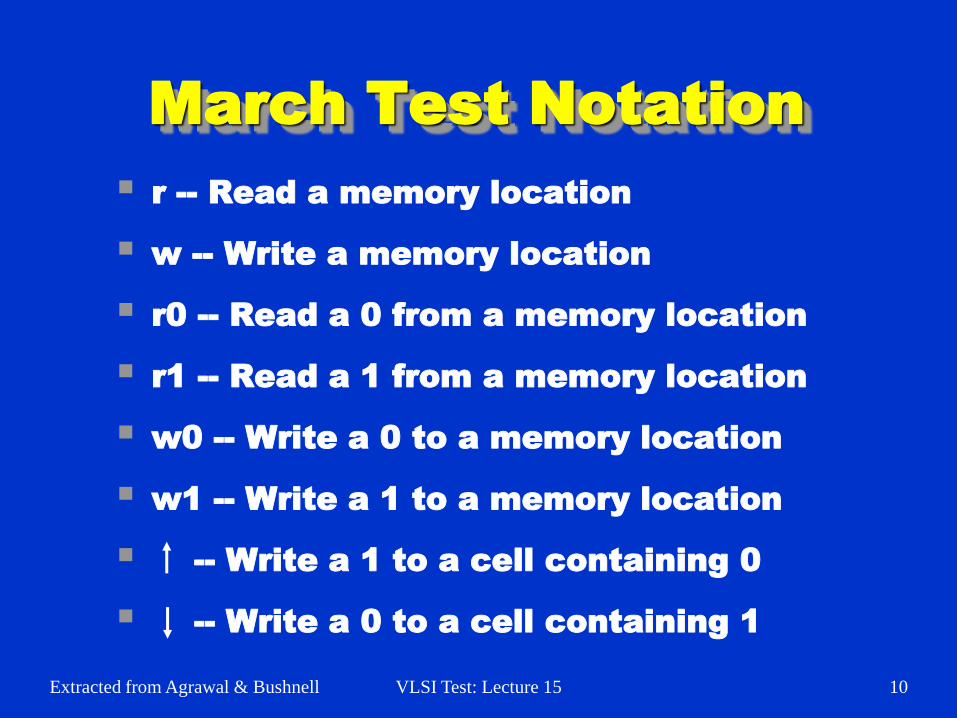
March Test Notation
r -- Read a memory location
w -- Write a memory location
r0 -- Read a 0 from a memory location
r1 -- Read a 1 from a memory location
w0 -- Write a 0 to a memory location
w1 -- Write a 1 to a memory location
-- Write a 1 to a cell containing 0
-- Write a 0 to a cell containing 1
Extracted from Agrawal & Bushnell VLSI Test: Lecture 15 11
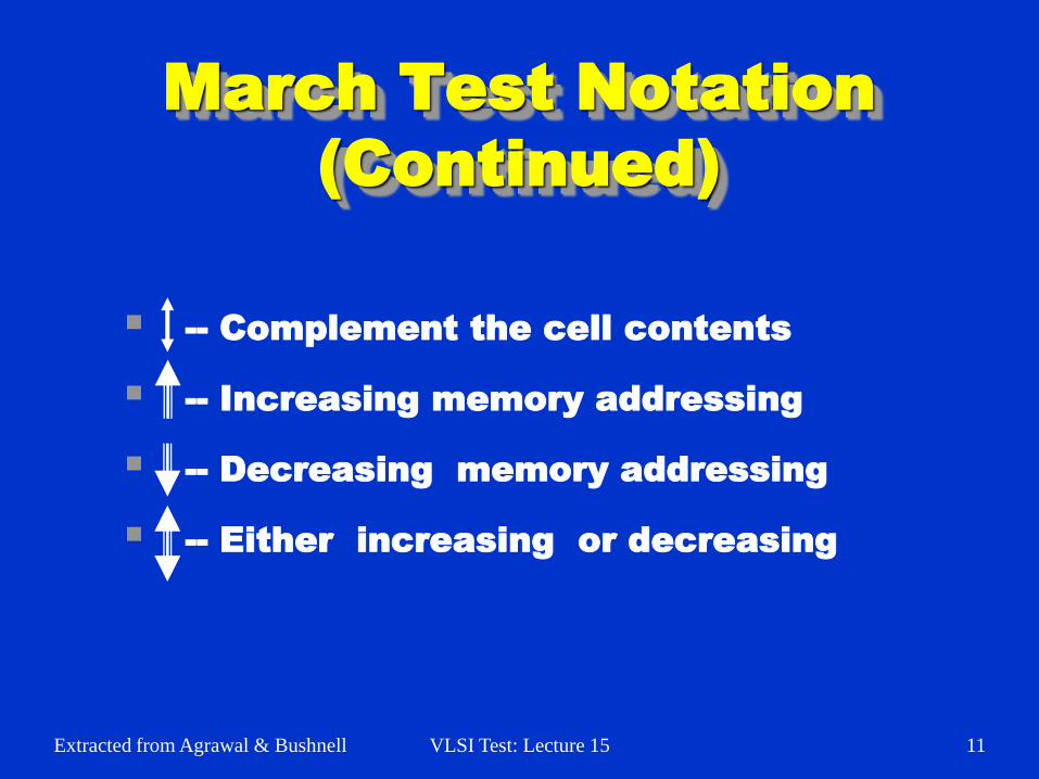
March Test Notation
(Continued)
-- Complement the cell contents
-- Increasing memory addressing
-- Decreasing memory addressing
-- Either increasing or decreasing
Extracted from Agrawal & Bushnell VLSI Test: Lecture 15 12
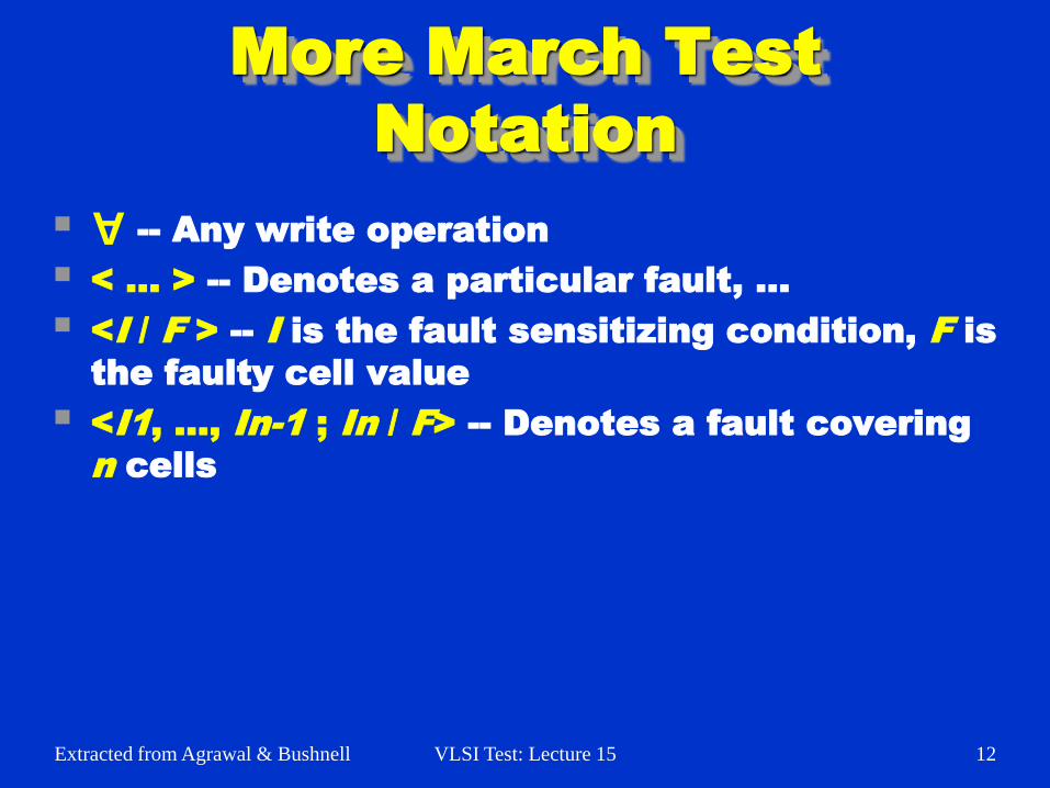
More March Test
Notation
-- Any write operation
< ... > -- Denotes a particular fault, ...
<I / F > -- I is the fault sensitizing condition, F is
the faulty cell value
<I1, ..., In-1 ; In / F> -- Denotes a fault covering
n cells
A
Extracted from Agrawal & Bushnell VLSI Test: Lecture 15 13
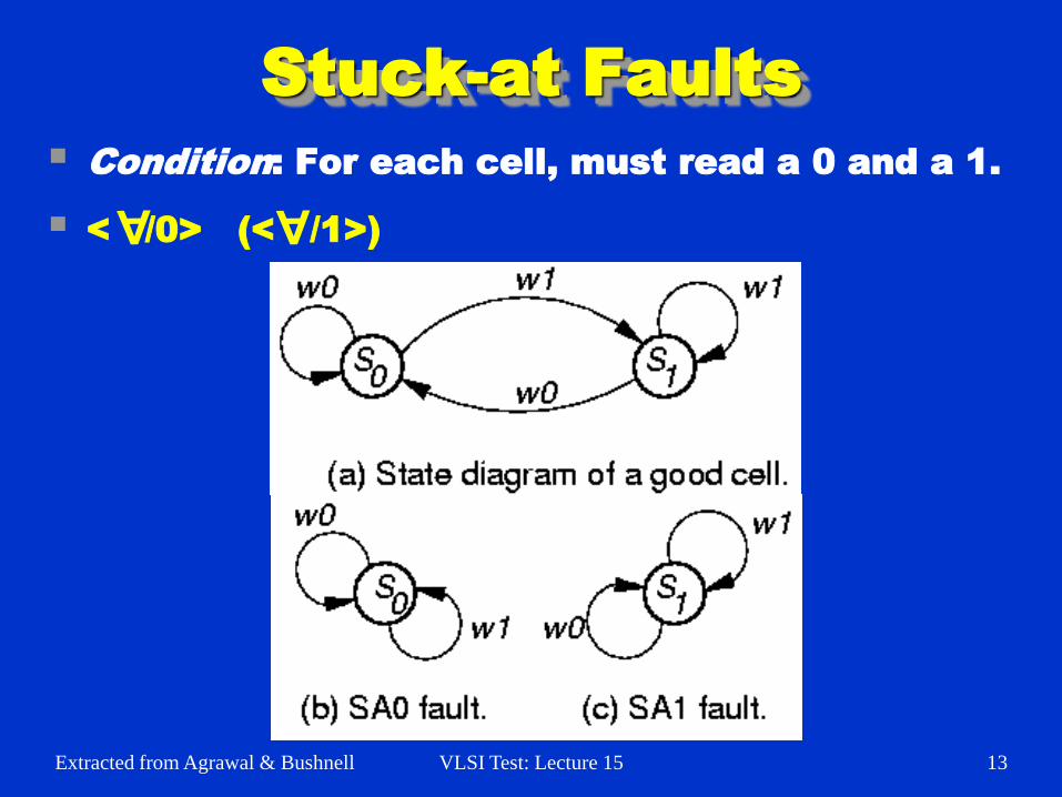
Stuck-at Faults
Condition: For each cell, must read a 0 and a 1.
< /0> (< /1>)

Extracted from Agrawal & Bushnell VLSI Test: Lecture 15 14
Transition Faults
Cell fails to make 0 1 or 1 0 transition
Condition: Each cell must undergo a transition
and a transition, and be read after such,
before undergoing any further transitions.
< /0>, < /1>
< /0> transition fault
Extracted from Agrawal & Bushnell VLSI Test: Lecture 15 15
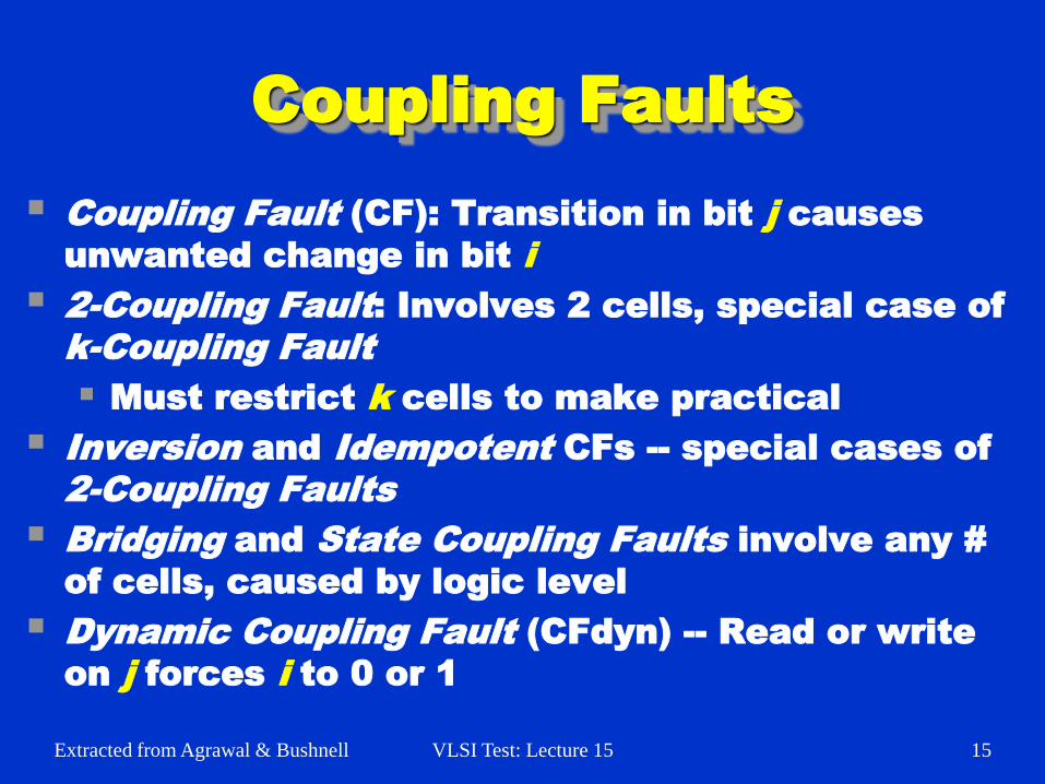
Coupling Faults
Coupling Fault (CF): Transition in bit j causes
unwanted change in bit i
2-Coupling Fault: Involves 2 cells, special case of
k-Coupling Fault
Must restrict k cells to make practical
Inversion and Idempotent CFs -- special cases of
2-Coupling Faults
Bridging and State Coupling Faults involve any #
of cells, caused by logic level
Dynamic Coupling Fault (CFdyn) -- Read or write
on j forces i to 0 or 1
Extracted from Agrawal & Bushnell VLSI Test: Lecture 15 16
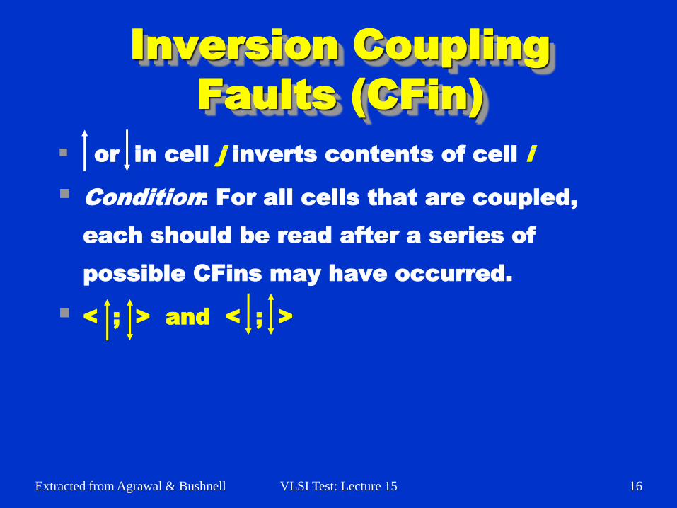
Inversion Coupling
Faults (CFin)
or in cell j inverts contents of cell i
Condition: For all cells that are coupled,
each should be read after a series of
possible CFins may have occurred.
< ; > and < ; >
Extracted from Agrawal & Bushnell VLSI Test: Lecture 15 17
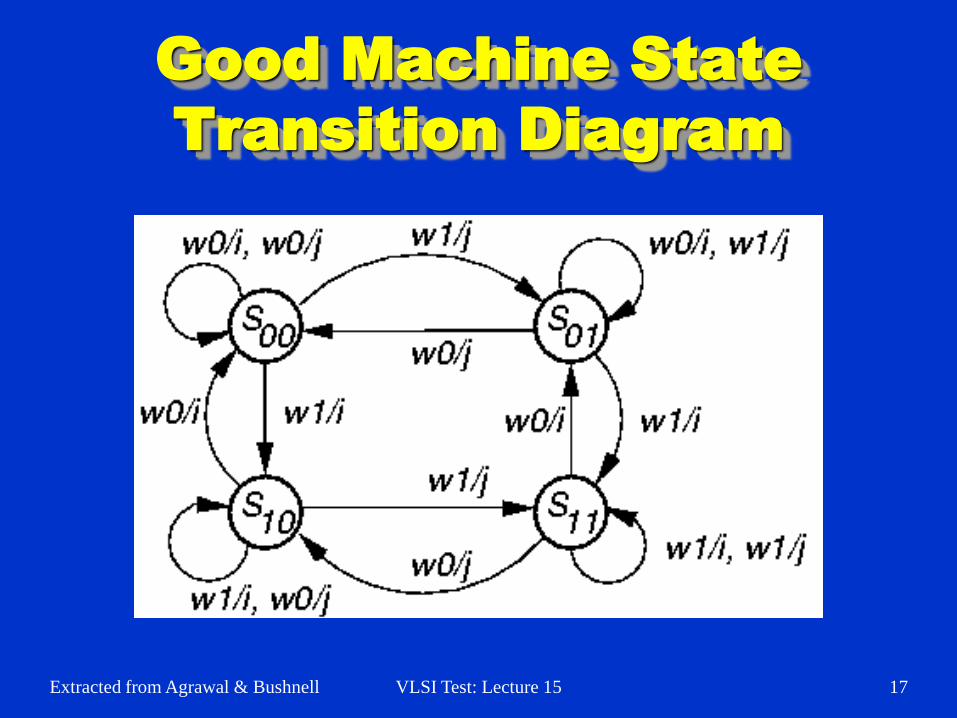
Good Machine State
Transition Diagram
Extracted from Agrawal & Bushnell VLSI Test: Lecture 15 18
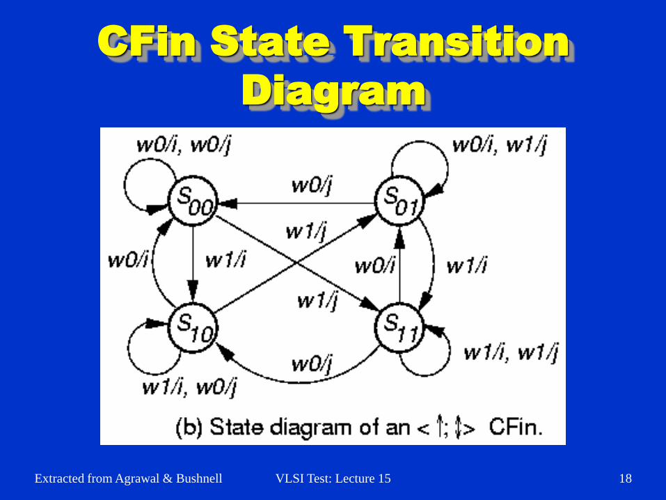
CFin State Transition
Diagram
Extracted from Agrawal & Bushnell VLSI Test: Lecture 15 19
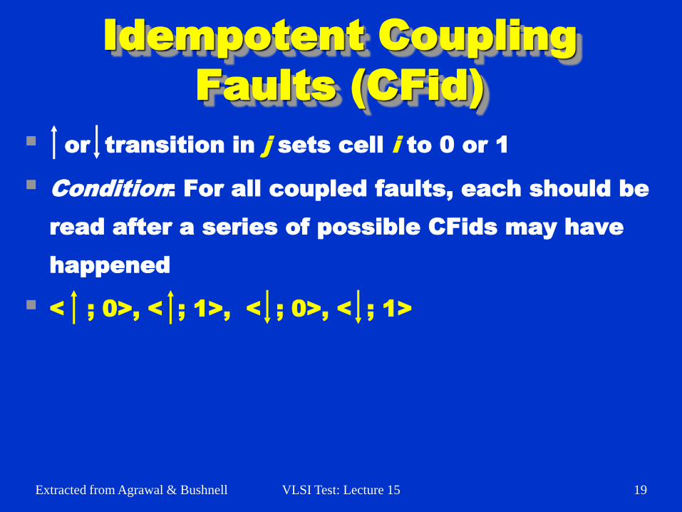
Idempotent Coupling
Faults (CFid)
or transition in j sets cell i to 0 or 1
Condition: For all coupled faults, each should be
read after a series of possible CFids may have
happened
< ; 0>, < ; 1>, < ; 0>, < ; 1>
Extracted from Agrawal & Bushnell VLSI Test: Lecture 15 20
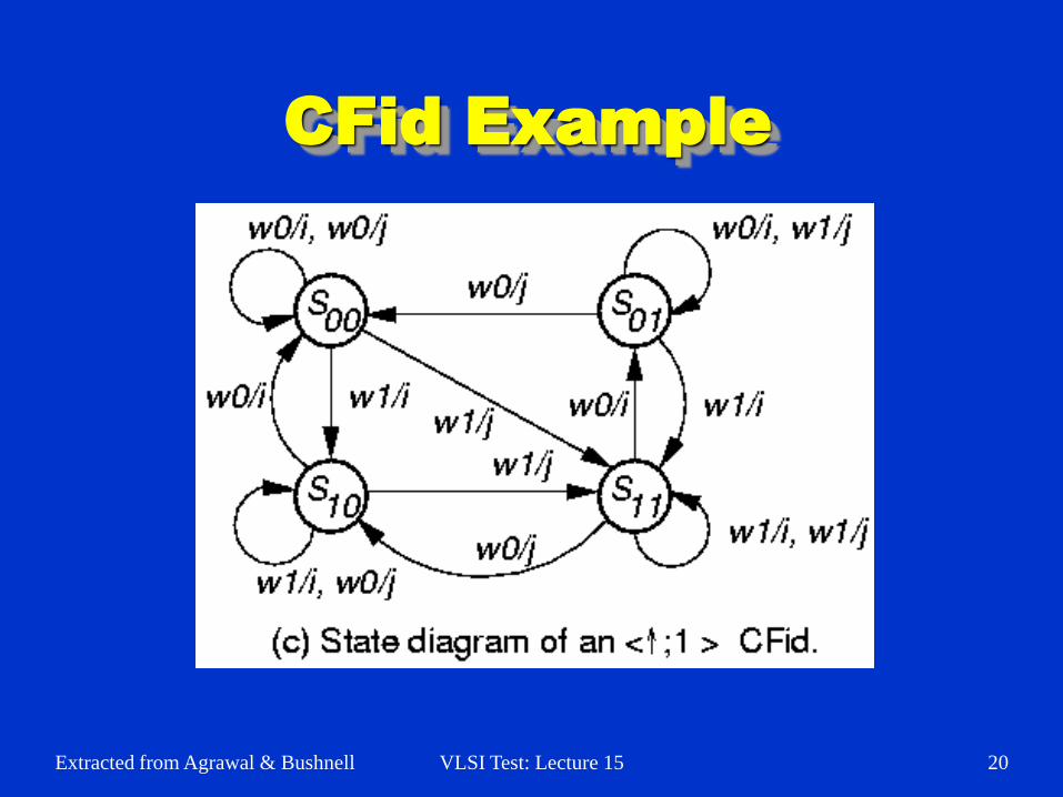
CFid Example
Extracted from Agrawal & Bushnell VLSI Test: Lecture 15 21
Dynamic Coupling
Faults (CFdyn)
Read or write in cell of 1 word forces cell in
different word to 0 or 1
<r0 | w0 ; 0>, <r0 | w0 ; 1>,
< r1 | w1 ; 0>, and <r1 | w1; 1>
| Denotes ―OR‖ of two operations
More general than CFid, because a CFdyn
can be sensitized by any read or write
operation
Extracted from Agrawal & Bushnell VLSI Test: Lecture 15 22
Bridging Faults
Short circuit between 2+ cells or lines
0 or 1 state of coupling cell, rather than coupling
cell transition, causes coupled cell change
Bidirectional fault -- i affects j, j affects i
AND Bridging Faults (ABF):
< 0,0 / 0,0 >, <0,1 / 0,0 >, <1,0 / 0,0>, <1,1 / 1,1>
OR Bridging Faults (OBF):
< 0,0 / 0,0 >, <0,1 / 1,1 >, <1,0 / 1,1>, <1,1 / 1,1>
Extracted from Agrawal & Bushnell VLSI Test: Lecture 15 23
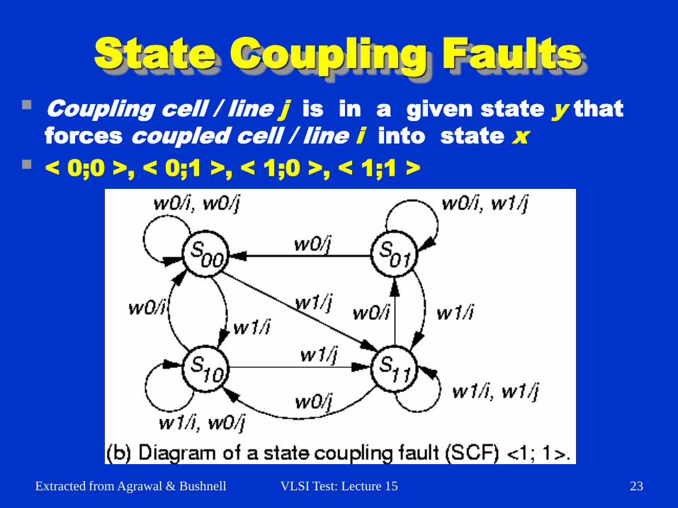
State Coupling Faults
Coupling cell / line j is in a given state y that
forces coupled cell / line i into state x
< 0;0 >, < 0;1 >, < 1;0 >, < 1;1 >
Extracted from Agrawal & Bushnell VLSI Test: Lecture 15 24
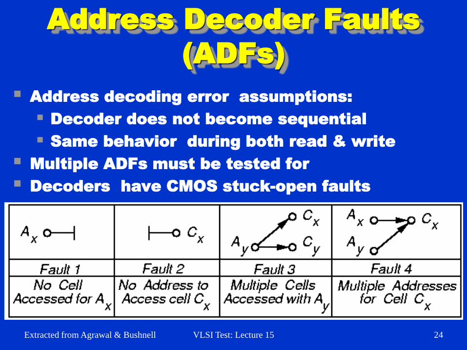
Address Decoder Faults
(ADFs)
Address decoding error assumptions:
Decoder does not become sequential
Same behavior during both read & write
Multiple ADFs must be tested for
Decoders have CMOS stuck-open faults

Extracted from Agrawal & Bushnell VLSI Test: Lecture 15 25
Functional RAM Testing
with March Tests
March Tests can detect AFs
Conditions for AF detection:
Need ( r x, w x)
Need ( r x, w x)
In the following March tests, addressing
orders can be interchanged

Extracted from Agrawal & Bushnell VLSI Test: Lecture 15 26
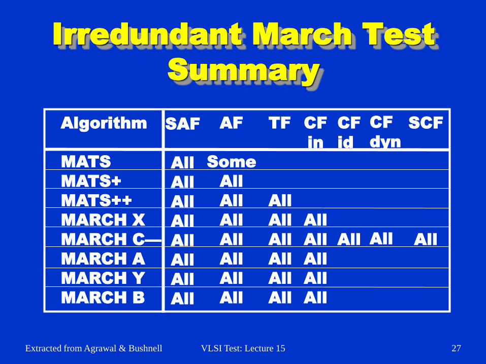
Irredundant March Tests
Algorithm
MATS
MATS+
MATS++
MARCH X
MARCH
C—
MARCH A
MARCH Y
MARCH B
Description
{ (w0); (r0, w1); (r1) }
{ (w0); (r0, w1); (r1, w0) }
{ (w0); (r0, w1); (r1, w0, r0) }
{ (w0); (r0, w1); (r1, w0); (r0) }
{ (w0); (r0, w1); (r1, w0);
(r0, w1); (r1, w0); (r0) }
{ (w0); (r0, w1, w0, w1); (r1, w0, w1);
(r1, w0, w1, w0); (r0, w1, w0) }
{ (w0); (r0, w1, r1); (r1, w0, r0); (r0) }
{ (w0); (r0, w1, r1, w0, r0, w1);
(r1, w0, w1); (r1, w0, w1, w0);
(r0, w1, w0) }
Extracted from Agrawal & Bushnell VLSI Test: Lecture 15 27
Irredundant March Test
Summary
Algorithm
MATS
MATS+
MATS++
MARCH X
MARCH C—
MARCH A
MARCH Y
MARCH B
SAF
All
All
All
All
All
All
All
All
AF
Some
All
All
All
All
All
All
All
TF
All
All
All
All
All
All
CF
in
All
All
All
All
All
CF
id
All
CF
dyn
All
SCF
All
Extracted from Agrawal & Bushnell VLSI Test: Lecture 15 28
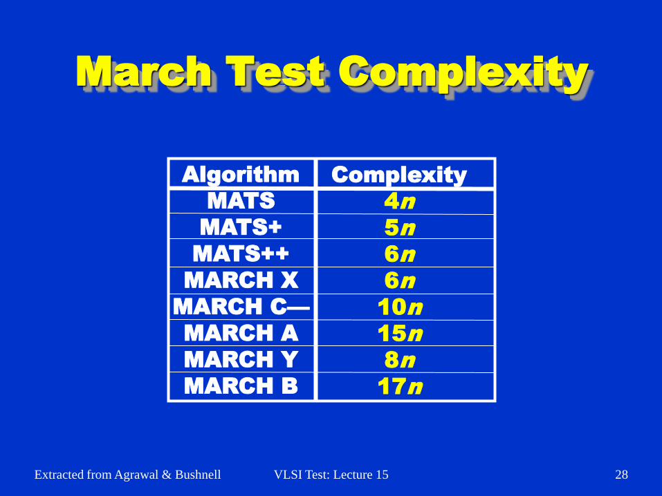
March Test Complexity
Algorithm
MATS
MATS+
MATS++
MARCH X
MARCH C—
MARCH A
MARCH Y
MARCH B
Complexity
4n
5n
6n
6n
10n
15n
8n
17n
Extracted from Agrawal & Bushnell VLSI Test: Lecture 15 29
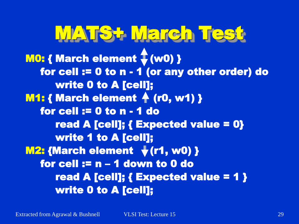
MATS+ March Test
M0: { March element (w0) }
for cell := 0 to n - 1 (or any other order) do
write 0 to A [cell];
M1: { March element (r0, w1) }
for cell := 0 to n - 1 do
read A [cell]; { Expected value = 0}
write 1 to A [cell];
M2: {March element (r1, w0) }
for cell := n – 1 down to 0 do
read A [cell]; { Expected value = 1 }
write 0 to A [cell];
Extracted from Agrawal & Bushnell VLSI Test: Lecture 15 30
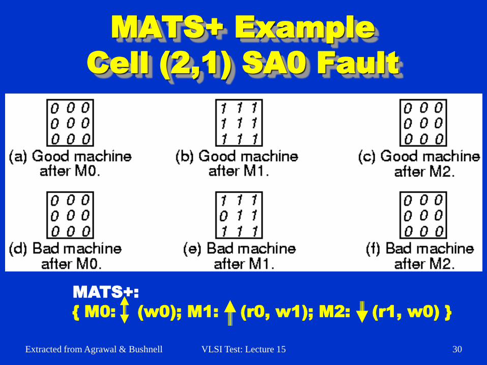
MATS+ Example
Cell (2,1) SA0 Fault
MATS+:
{ M0: (w0); M1: (r0, w1); M2: (r1, w0) }

Extracted from Agrawal & Bushnell VLSI Test: Lecture 15 31
MATS+ Example
Cell (2, 1) SA1 Fault
MATS+:
{ M0: (w0); M1: (r0, w1); M2: (r1, w0) }
Extracted from Agrawal & Bushnell VLSI Test: Lecture 15 32
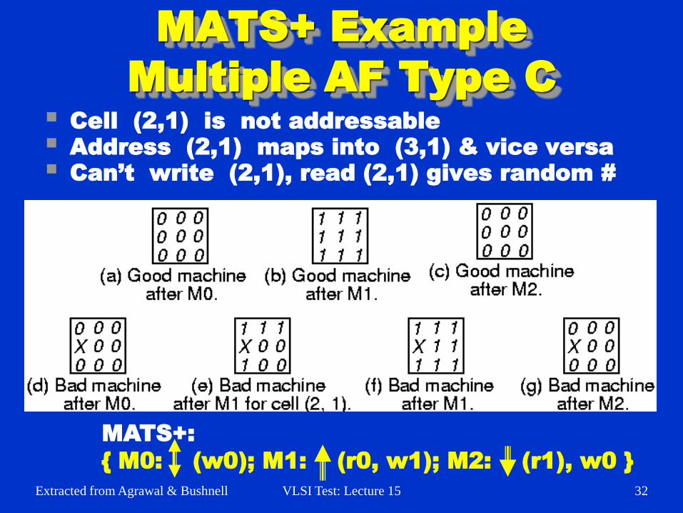
MATS+ Example
Multiple AF Type C
Cell (2,1) is not addressable
Address (2,1) maps into (3,1) & vice versa
Can’t write (2,1), read (2,1) gives random #
MATS+:
{ M0: (w0); M1: (r0, w1); M2: (r1), w0 }
Extracted from Agrawal & Bushnell VLSI Test: Lecture 15 33
Memory Test Summary
More complex fault models are essential
Combination of tests is essential:
March
DC Parametric
AC Parametric
Related areas of memory test
BIST – standard practice for embedded memories
Repairable memories – redundancy to enhance yield
Extracted from Agrawal & Bushnell VLSI Test: Lecture 15 34
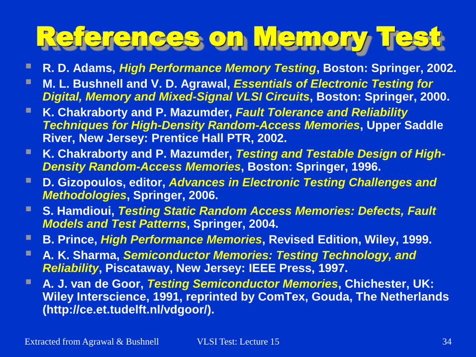
References on Memory Test
R. D. Adams, High Performance Memory Testing, Boston: Springer, 2002.
M. L. Bushnell and V. D. Agrawal, Essentials of Electronic Testing for Digital, Memory and Mixed-Signal VLSI Circuits, Boston: Springer, 2000.
K. Chakraborty and P. Mazumder, Fault Tolerance and Reliability Techniques for High-Density Random-Access Memories, Upper Saddle River, New Jersey: Prentice Hall PTR, 2002.
K. Chakraborty and P. Mazumder, Testing and Testable Design of High-Density Random-Access Memories, Boston: Springer, 1996.
D. Gizopoulos, editor, Advances in Electronic Testing Challenges and Methodologies, Springer, 2006.
S. Hamdioui, Testing Static Random Access Memories: Defects, Fault Models and Test Patterns, Springer, 2004.
B. Prince, High Performance Memories, Revised Edition, Wiley, 1999.
A. K. Sharma, Semiconductor Memories: Testing Technology, and Reliability, Piscataway, New Jersey: IEEE Press, 1997.
A. J. van de Goor, Testing Semiconductor Memories, Chichester, UK: Wiley Interscience, 1991, reprinted by ComTex, Gouda, The Netherlands (http://ce.et.tudelft.nl/vdgoor/).


![[XLS] · Web view005B PC Memory - 4MB 005C PC Memory - 6MB 005D PC Memory - 8MB 005E PC Memory - 10MB 005F PC Memory - 12MB 005G PC Memory - 14MB 005H PC Memory - 16MB 005I PC Memory](https://img.pdfslide.us/doc/110x75/5ab13df97f8b9ac66c8c4031/xls-view005b-pc-memory-4mb-005c-pc-memory-6mb-005d-pc-memory-8mb-005e-pc.jpg)