Embed Size (px)
Citation preview
Lecture 7.0Lecture 7.0
Device Physics
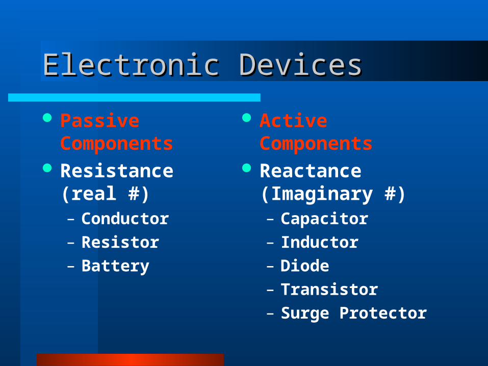
Electronic DevicesElectronic Devices
Passive Components
Resistance (real #)– Conductor– Resistor– Battery
Active Components
Reactance (Imaginary #)– Capacitor– Inductor– Diode– Transistor– Surge Protector
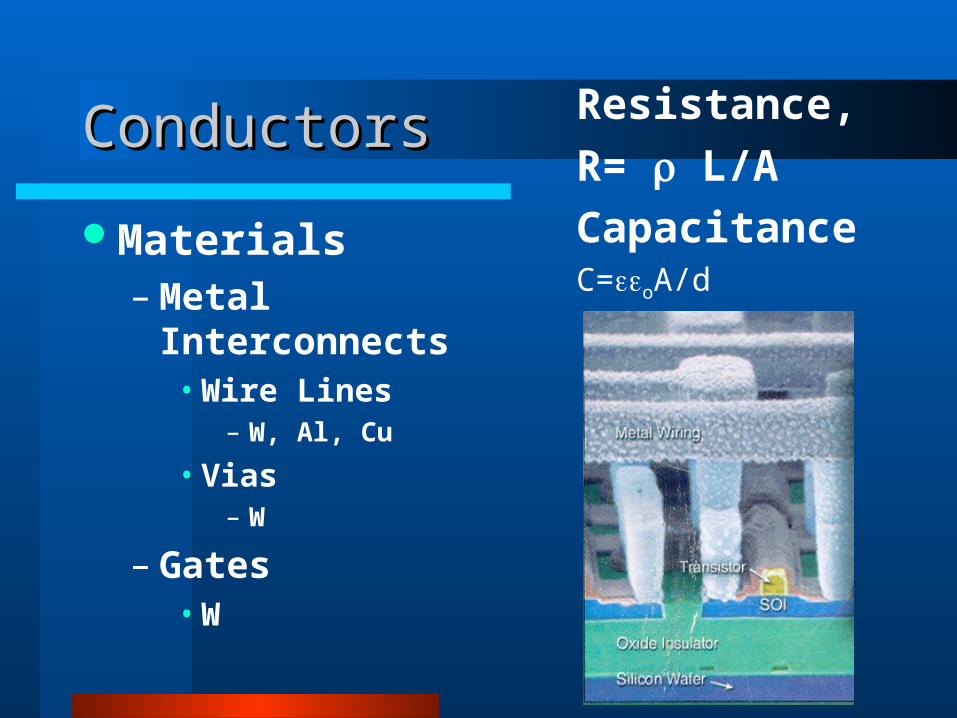
ConductorsConductors
Materials– Metal Interconnects
• Wire Lines– W, Al, Cu
• Vias– W
– Gates• W
Resistance,
R= L/A
CapacitanceC=oA/d
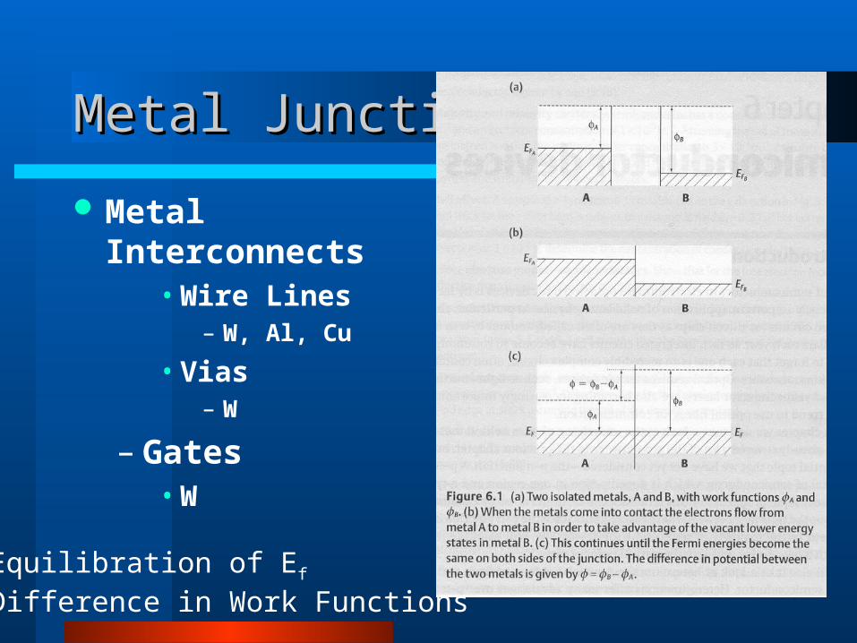
Metal JunctionsMetal Junctions
Metal Interconnects• Wire Lines
– W, Al, Cu
• Vias– W
– Gates• W
Equilibration of Ef
Difference in Work Functions
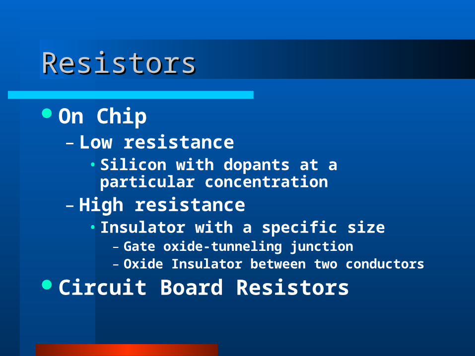
ResistorsResistors
On Chip– Low resistance
• Silicon with dopants at a particular concentration
– High resistance• Insulator with a specific size
– Gate oxide-tunneling junction– Oxide Insulator between two conductors
Circuit Board Resistors
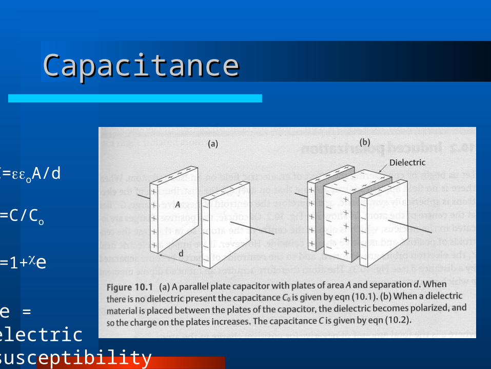
CapacitanceCapacitance
C=oA/d
=C/Co
=1+e
e =electric susceptibility
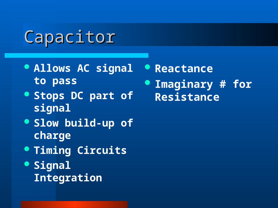
CapacitorCapacitor
Allows AC signal to pass
Stops DC part of signal
Slow build-up of charge
Timing Circuits Signal Integration
Reactance Imaginary # for
Resistance
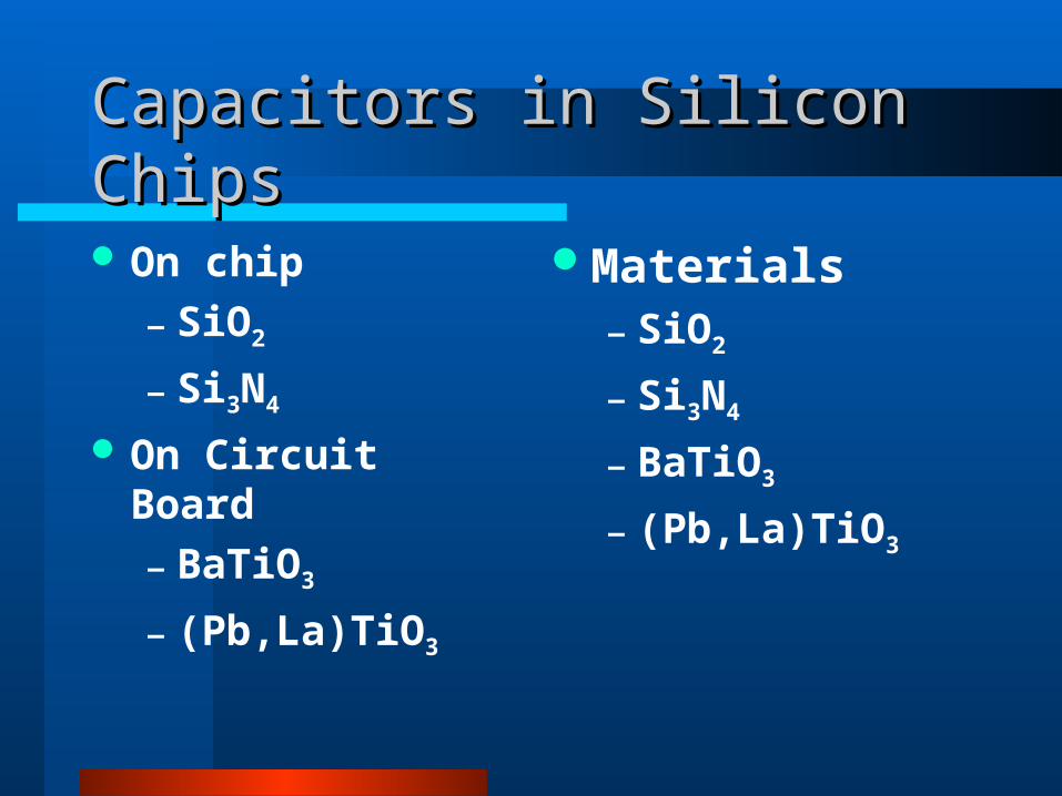
Capacitors in Silicon ChipsCapacitors in Silicon Chips
On chip
– SiO2
– Si3N4
On Circuit Board
– BaTiO3
– (Pb,La)TiO3
Materials– SiO2
– Si3N4
– BaTiO3
– (Pb,La)TiO3
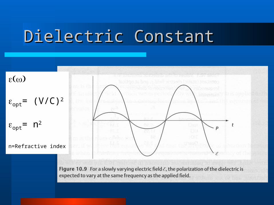
Dielectric ConstantDielectric Constant
opt= (V/C)2
opt= n2
n=Refractive index
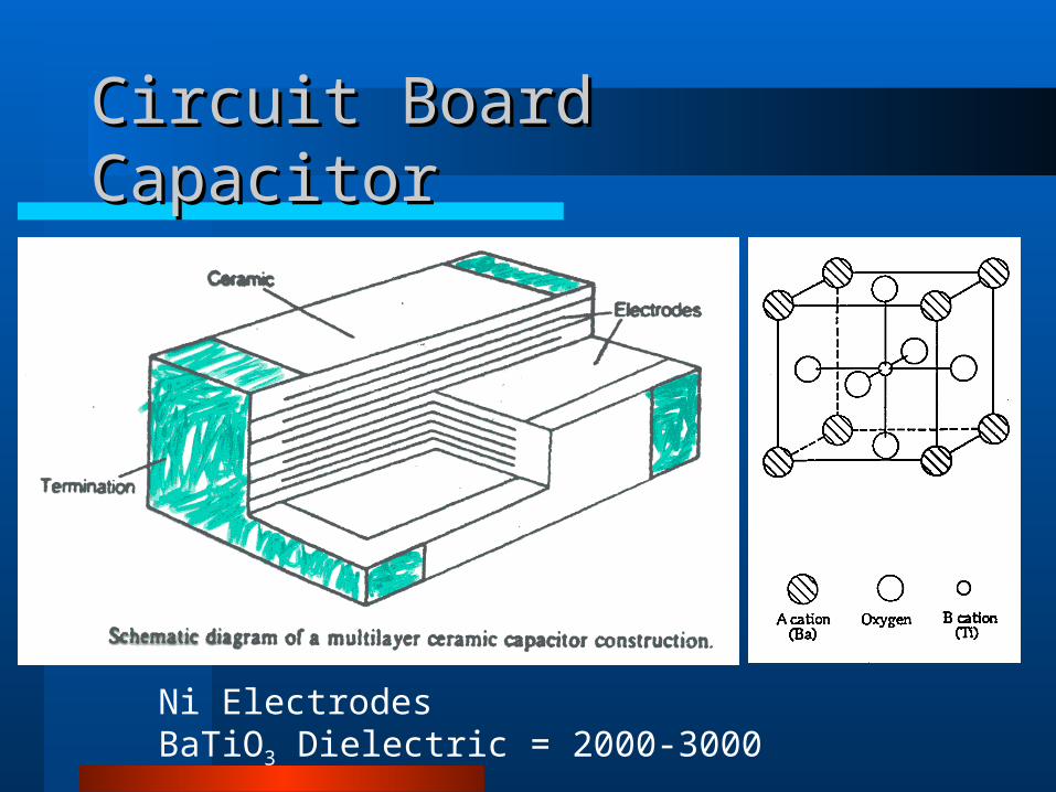
Circuit Board CapacitorCircuit Board Capacitor
Ni ElectrodesBaTiO3 Dielectric = 2000-3000
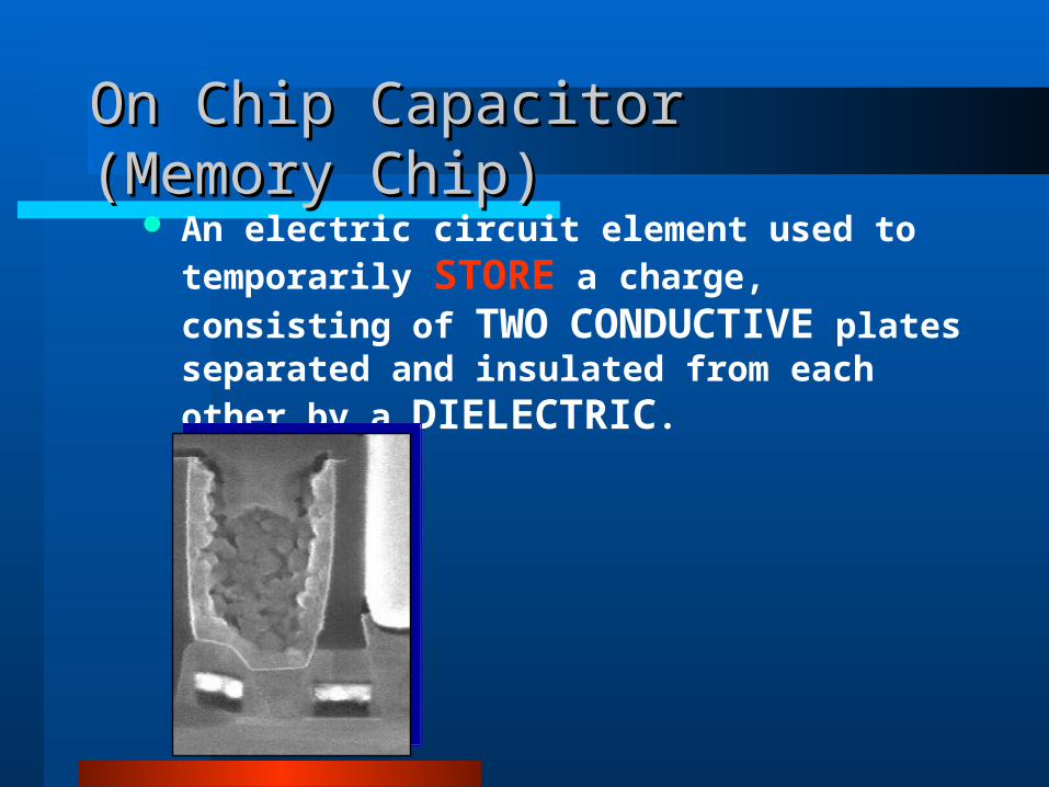
On Chip Capacitor (Memory Chip)On Chip Capacitor (Memory Chip) An electric circuit element used to temporarily
STORE a charge, consisting of TWO
CONDUCTIVE plates separated and insulated
from each other by a DIELECTRIC.
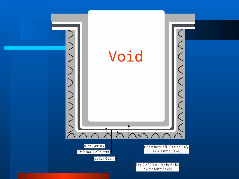
W et G ate O x
D ie lectric C ell N itride
N ative O xide
C onta iner C e ll - C om bo P o ly17 M asking Leve l
Top C e ll P la te - Ins itu P o ly3(52 M asking Leve l)
Void
InductorInductor
What is it?– Coil of wire
Not used on ChipOn Circuit Board
– Used oftenReactance
– (imaginary # for resistance)
P-n junctionP-n junction
One way flow of current – Diode bridge
• Converts AC to DC
Photo Diode Laser
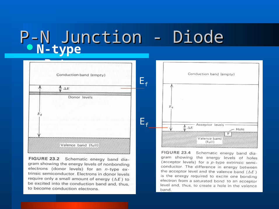
P-N Junction - DiodeP-N Junction - DiodeN-type P-type
Ef
Ef
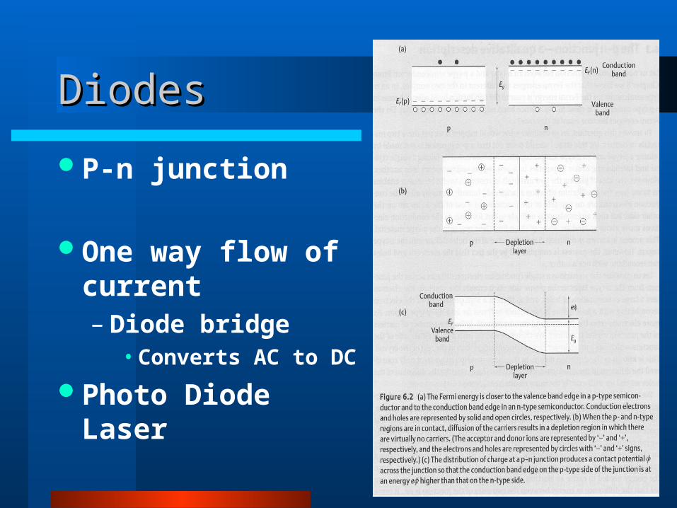
DiodesDiodes
P-n junction
One way flow of current – Diode bridge
• Converts AC to DC
Photo Diode Laser
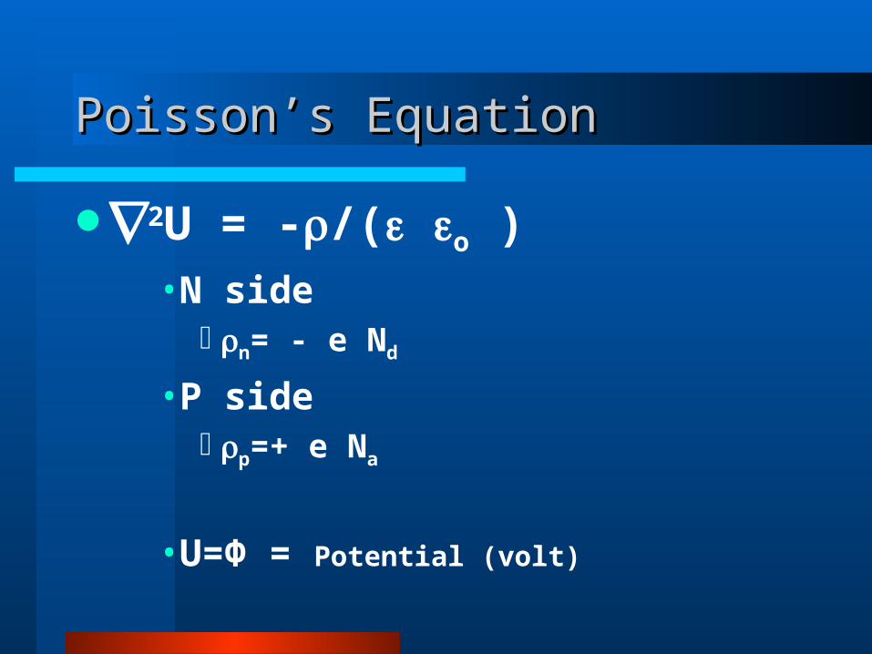
Poisson’s EquationPoisson’s Equation
2U = -/( o )• N side
n= - e Nd
• P side p=+ e Na
• U=Φ = Potential (volt)
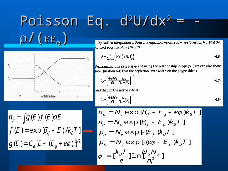
Poisson Eq. dPoisson Eq. d22UU/dx/dx2 2 = -= -/(/(oo) )
]ln[][
])exp[(
])exp[(
])exp[(
])exp[(
2i
daB
Bfvp
Bfvn
Bgfcn
Bgfcp
n
NN
e
Tk
TkEeNp
TkENp
TkEENn
TkeEENn
2/1)]([)(
]/)exp[()(
)()(
eEECEg
TkEEEf
dEEfEgn
ge
Bf
p
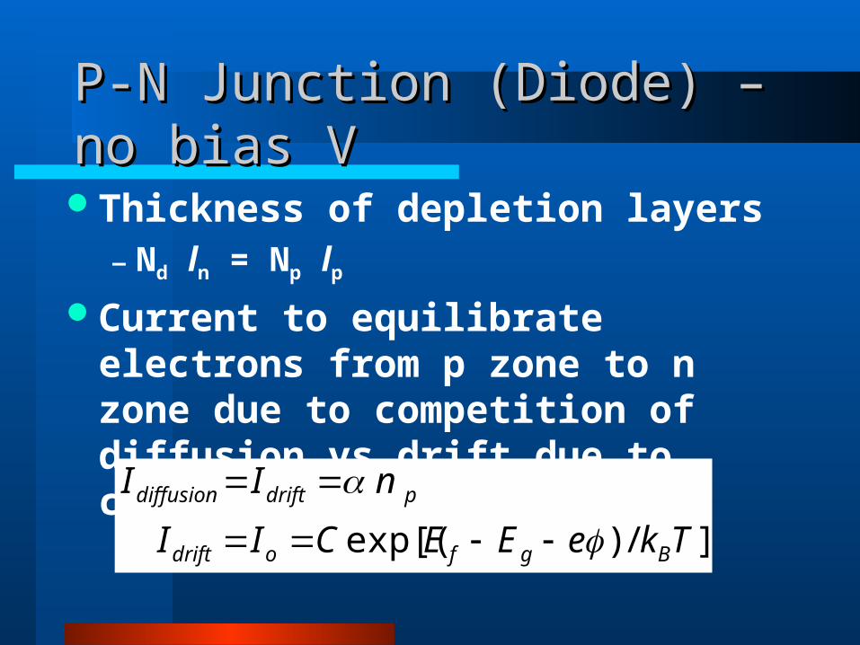
P-N Junction (Diode) – no bias VP-N Junction (Diode) – no bias V
Thickness of depletion layers– Nd ln = Np lp
Current to equilibrate electrons from p zone to n zone due to competition of diffusion vs drift due to contact Ф.
]/)exp[( TkeEECII
nII
Bgfodrift
pdriftdiffusion
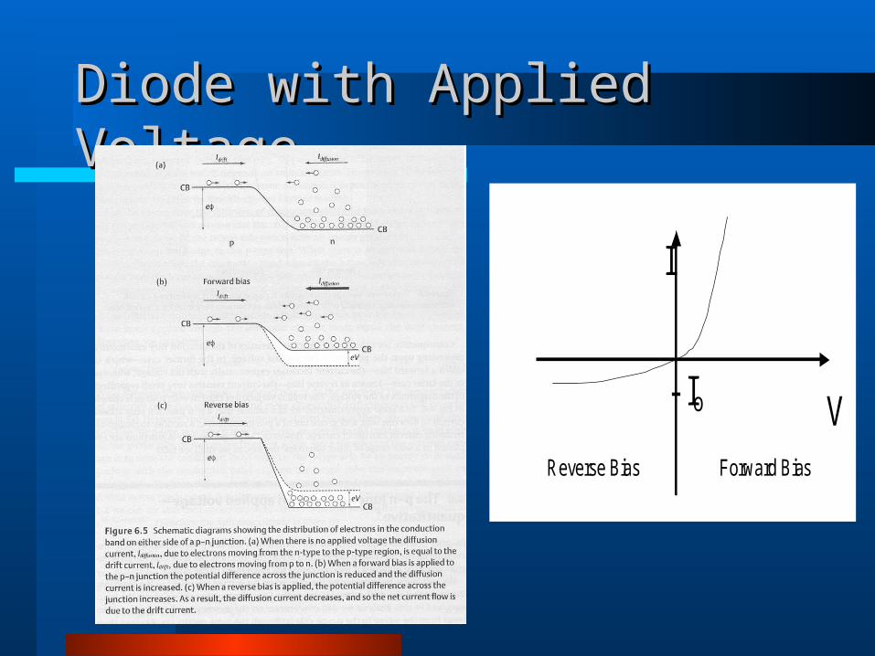
Diode with Applied VoltageDiode with Applied Voltage
I
V Reverse Bias Forward Bias
- Io
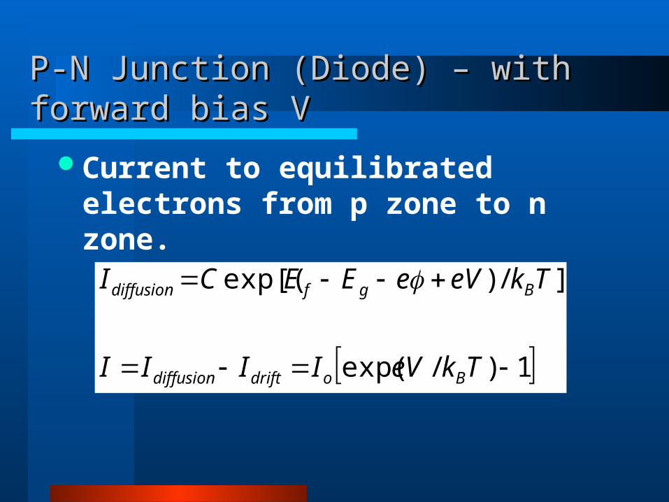
P-N Junction (Diode) – with forward bias VP-N Junction (Diode) – with forward bias V
Current to equilibrated electrons from p zone to n zone.
1)/exp(
]/)exp[(
TkeVIIII
TkeVeEECI
Bodriftdiffusion
Bgfdiffusion
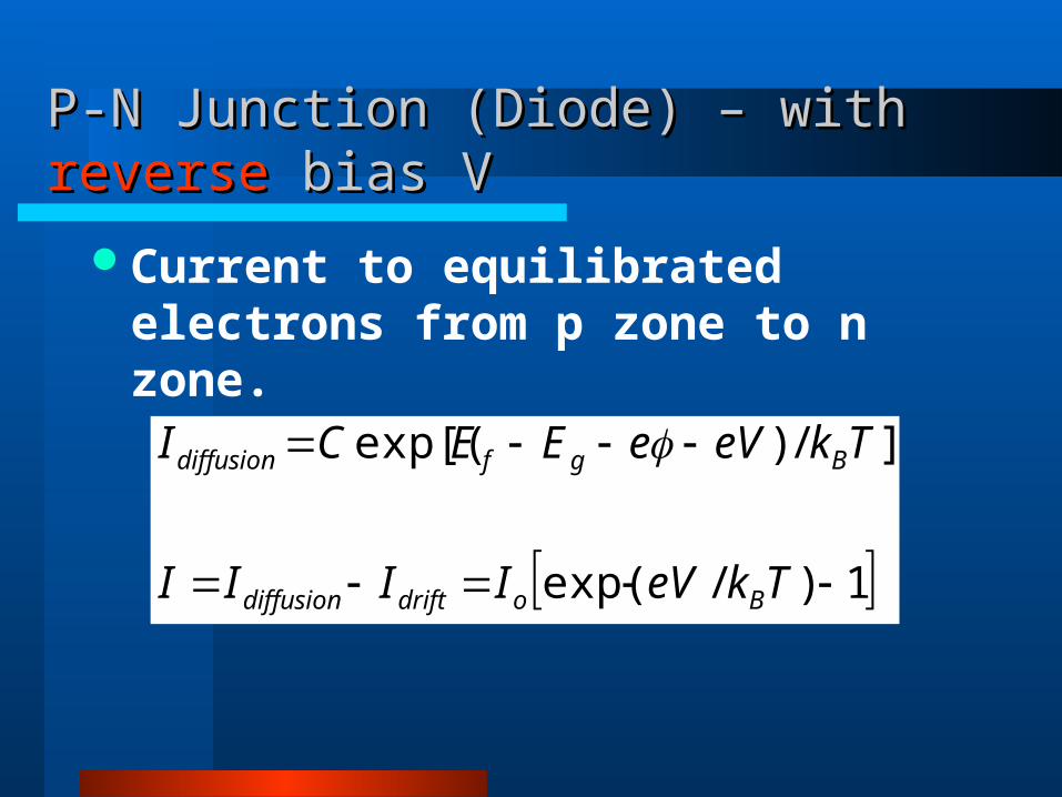
P-N Junction (Diode) – with P-N Junction (Diode) – with reversereverse bias V bias V
Current to equilibrated electrons from p zone to n zone.
1)/exp(
]/)exp[(
TkeVIIII
TkeVeEECI
Bodriftdiffusion
Bgfdiffusion
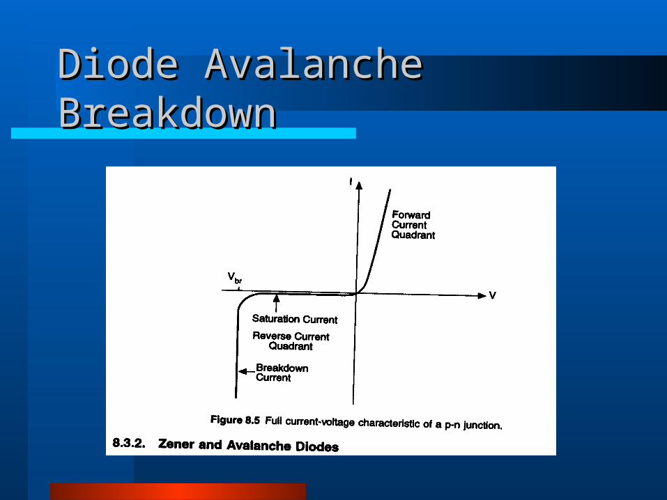
Diode Avalanche BreakdownDiode Avalanche Breakdown
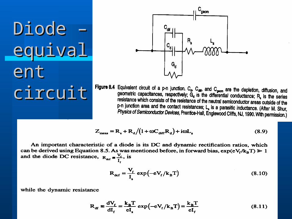
Diode – Diode – equivalent equivalent circuitcircuit

![Imaginary Phone: Learning Imaginary Interfaces by ... · Imaginary Phone: Learning Imaginary Interfaces by ... Our depth camera is a PMD[vision] CamCube that provides frames at 40Hz](https://img.pdfslide.us/doc/110x75/5ae222be7f8b9a097a8c8939/imaginary-phone-learning-imaginary-interfaces-by-phone-learning-imaginary.jpg)