Embed Size (px)
Citation preview
Vorlesung Uni Basel, FS2017
Molecular and carbon-based electronic systems
Lecture 7: Graphene
structure, fabrication, characterization
Examples: nanogaps, QHE
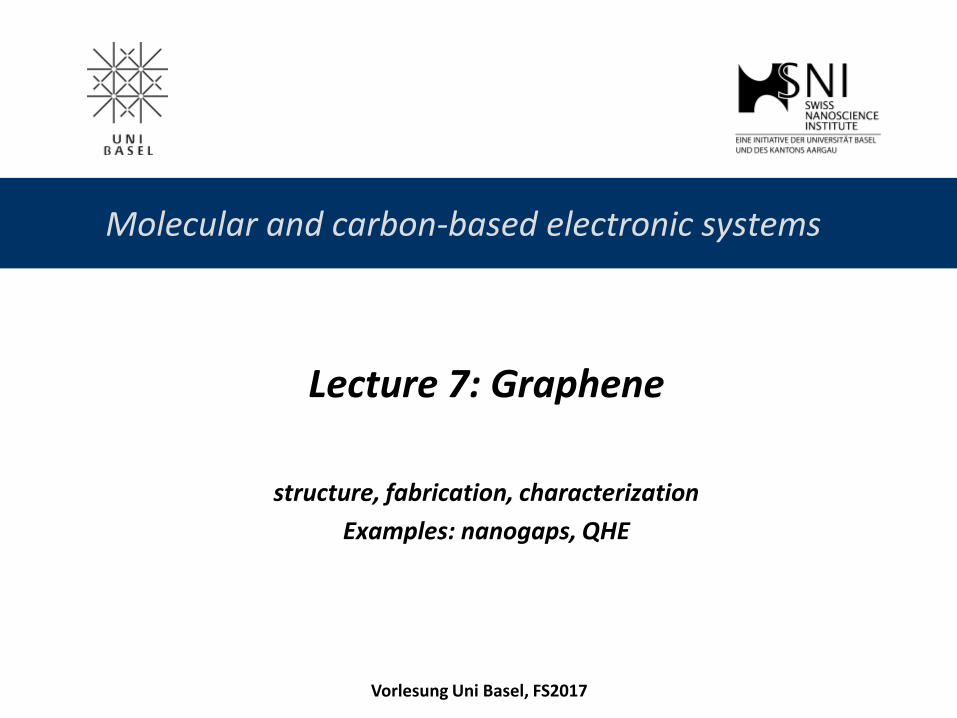
• graphene structure
• fabrication and CVD growth
• characterization: Raman spectroscopy
Examples
• graphene electroburning for molecular junctions
• Quantum Hall Effect
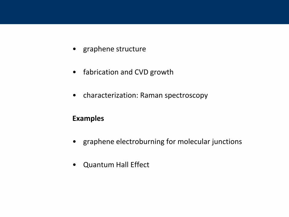
graphene structure: honeycomb lattice
vectors connecting a site on the A sublattice with
a nearest neighbor (nn) on the B sublattice
C-C bond: a 0.142nm
density of C atoms
Auc= 33a/2 = 0.051nm2
density of p electrons 1 p e / C atom not involved in s bond
Goerbig et al., Castro Neto et al., Rev. Mod. Phys 2009
basis vectors of the triangular Bravais
lattice (2 atoms basis)
six second nearest neighbors
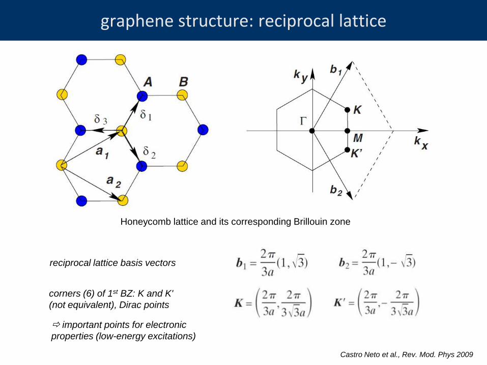
graphene structure: reciprocal lattice
reciprocal lattice basis vectors
Castro Neto et al., Rev. Mod. Phys 2009
Honeycomb lattice and its corresponding Brillouin zone
corners (6) of 1st BZ: K and K'
(not equivalent), Dirac points
important points for electronic
properties (low-energy excitations)
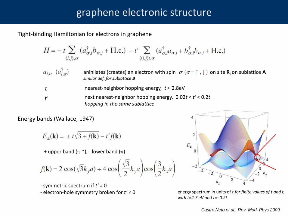
graphene electronic structure
Tight-binding Hamiltonian for electrons in graphene
anihilates (creates) an electron with spin on site Ri on sublattice A similar def. for sublattice B
t nearest-neighbor hopping energy, t 2.8eV
next nearest-neighbor hopping energy, 0.02t < t' < 0.2t hopping in the same sublattice
Castro Neto et al., Rev. Mod. Phys 2009
t'
Energy bands (Wallace, 1947)
+ upper band (p *), - lower band (p)
- symmetric spectrum if t' = 0 - electron-hole symmetry broken for t' ≠ 0 energy spectrum in units of t for finite values of t and t,
with t=2.7 eV and t=−0.2t
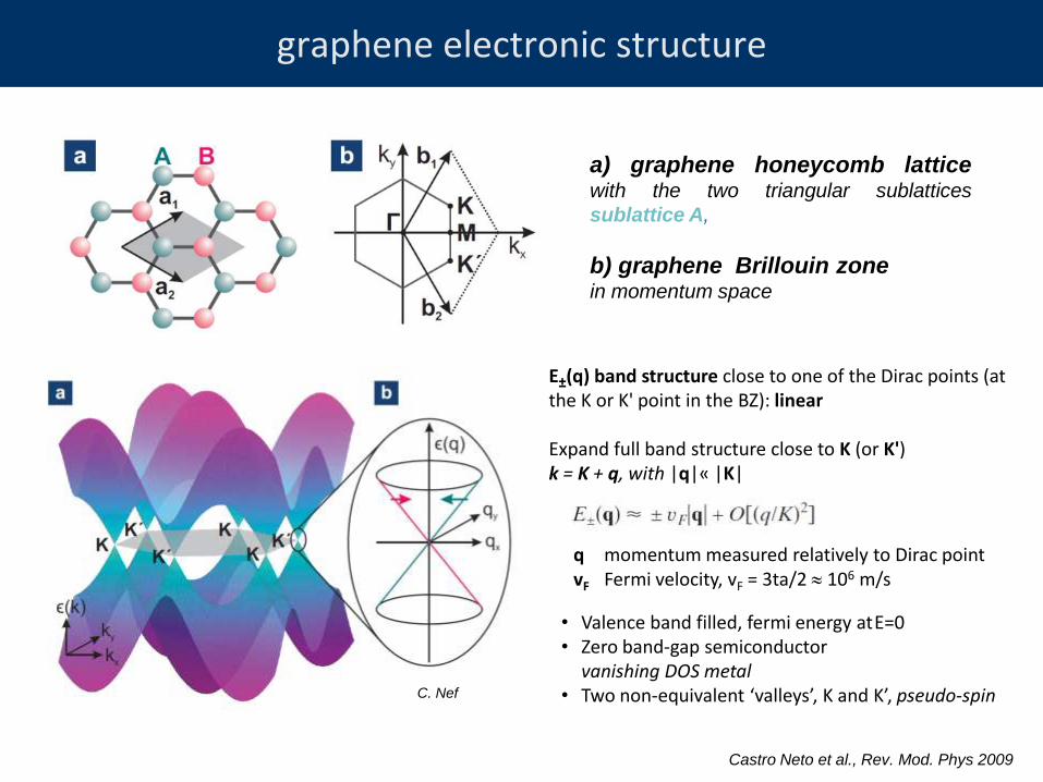
graphene electronic structure
C. Nef
a) graphene honeycomb lattice with the two triangular sublattices
sublattice A, sublattice B
b) graphene Brillouin zone in momentum space
Castro Neto et al., Rev. Mod. Phys 2009
• Valence band filled, fermi energy at E=0 • Zero band-gap semiconductor vanishing DOS metal • Two non-equivalent ‘valleys’, K and K’, pseudo-spin
E±(q) band structure close to one of the Dirac points (at the K or K' point in the BZ): linear Expand full band structure close to K (or K') k = K + q, with |q|« |K|
q momentum measured relatively to Dirac point vF Fermi velocity, vF = 3ta/2 106 m/s
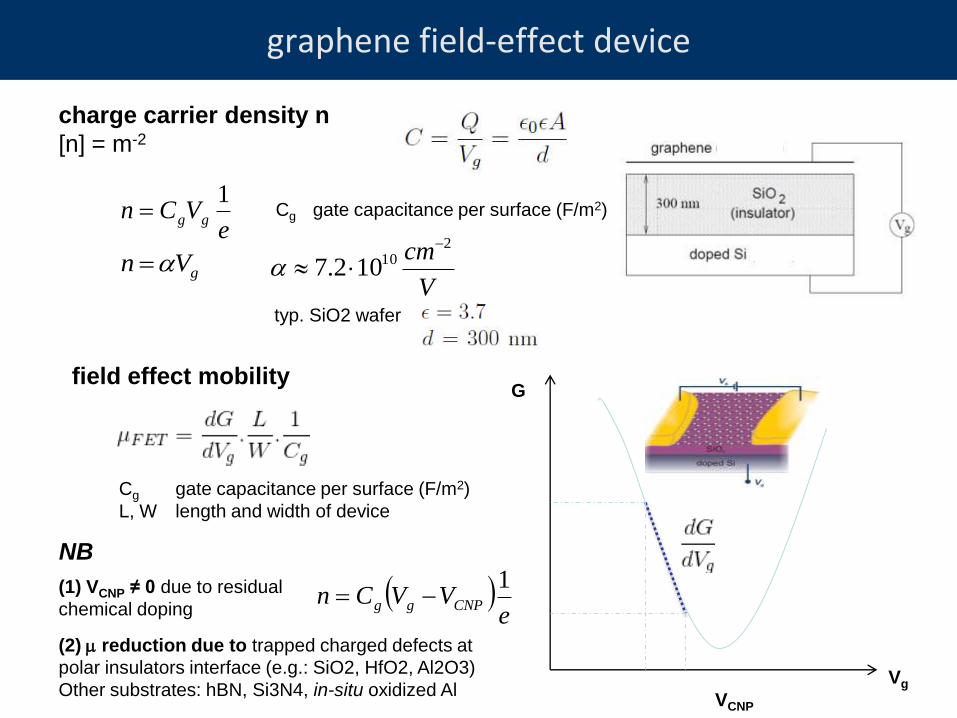
graphene field-effect device
Cg gate capacitance per surface (F/m2)
L, W length and width of device
field effect mobility
VCNP
Vg
G
typ. SiO2 wafer
charge carrier density n
[n] = m-2
Cg gate capacitance per surface (F/m2)
eVCn gg
1
gVn V
cm 210102.7
e
VVCn CNPgg
1(1) VCNP ≠ 0 due to residual
chemical doping
(2) m reduction due to trapped charged defects at
polar insulators interface (e.g.: SiO2, HfO2, Al2O3)
Other substrates: hBN, Si3N4, in-situ oxidized Al
NB
graphene-based devices
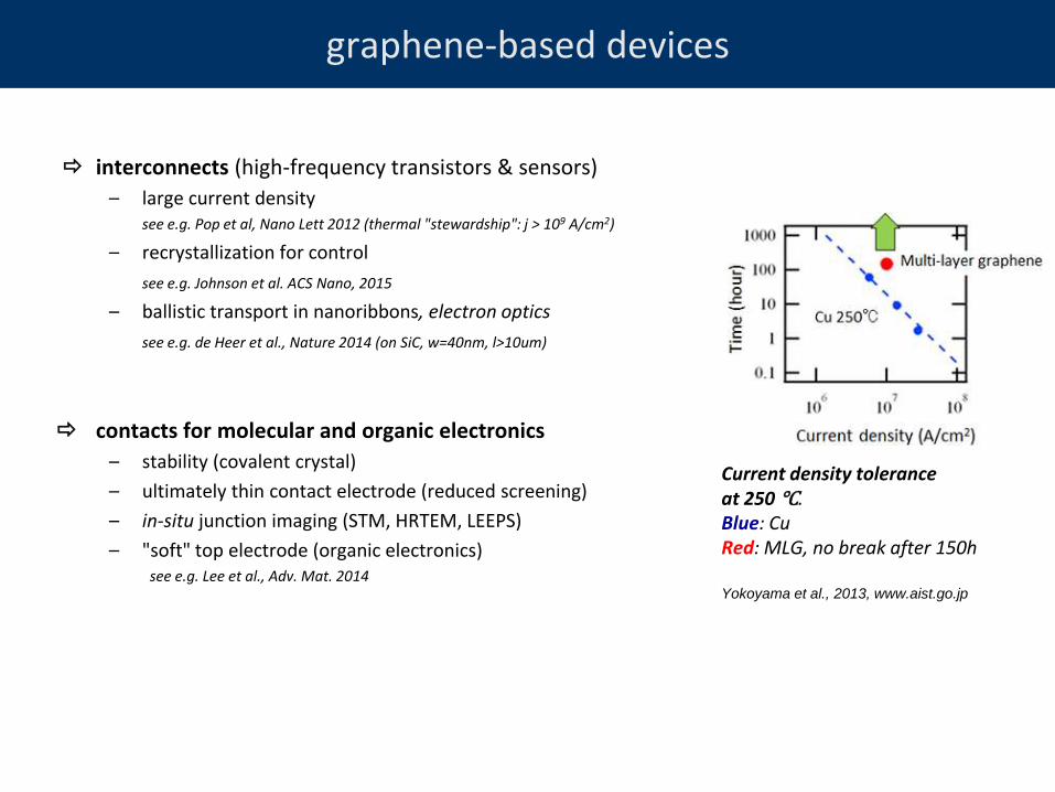
interconnects (high-frequency transistors & sensors)
– large current density see e.g. Pop et al, Nano Lett 2012 (thermal "stewardship": j > 109 A/cm2)
– recrystallization for control
see e.g. Johnson et al. ACS Nano, 2015
– ballistic transport in nanoribbons, electron optics
see e.g. de Heer et al., Nature 2014 (on SiC, w=40nm, l>10um)
contacts for molecular and organic electronics
– stability (covalent crystal)
– ultimately thin contact electrode (reduced screening)
– in-situ junction imaging (STM, HRTEM, LEEPS)
– "soft" top electrode (organic electronics) see e.g. Lee et al., Adv. Mat. 2014
Current density tolerance at 250 ℃. Blue: Cu Red: MLG, no break after 150h Yokoyama et al., 2013, www.aist.go.jp
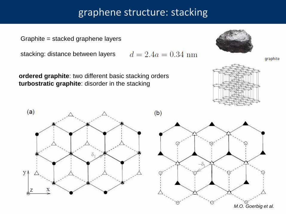
graphene structure: stacking
Graphite = stacked graphene layers
stacking: distance between layers
ordered graphite: two different basic stacking orders
turbostratic graphite: disorder in the stacking
M.O. Goerbig et al.
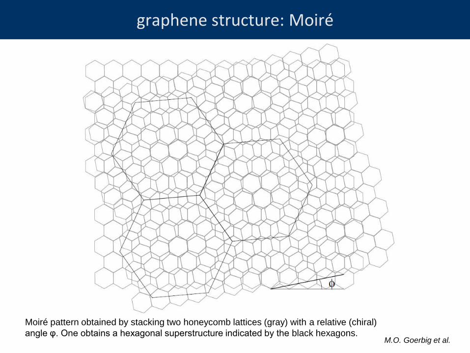
graphene structure: Moiré
M.O. Goerbig et al.
Moiré pattern obtained by stacking two honeycomb lattices (gray) with a relative (chiral)
angle φ. One obtains a hexagonal superstructure indicated by the black hexagons.
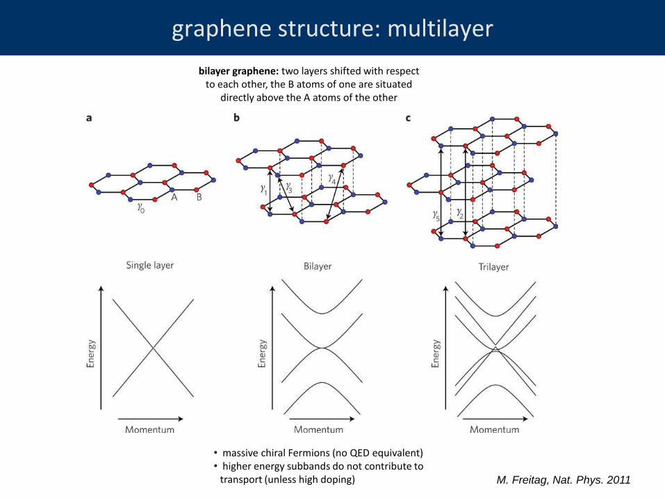
graphene structure: multilayer
M. Freitag, Nat. Phys. 2011
bilayer graphene: two layers shifted with respect to each other, the B atoms of one are situated
directly above the A atoms of the other
• massive chiral Fermions (no QED equivalent) • higher energy subbands do not contribute to
transport (unless high doping)
• graphene structure
• fabrication and CVD growth
• characterization: Raman spectroscopy
Examples
• graphene electroburning for molecular junctions
• Quantum Hall Effect
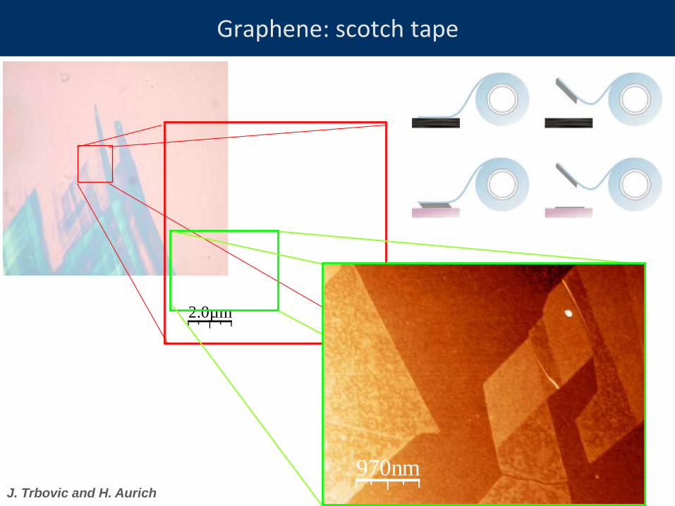
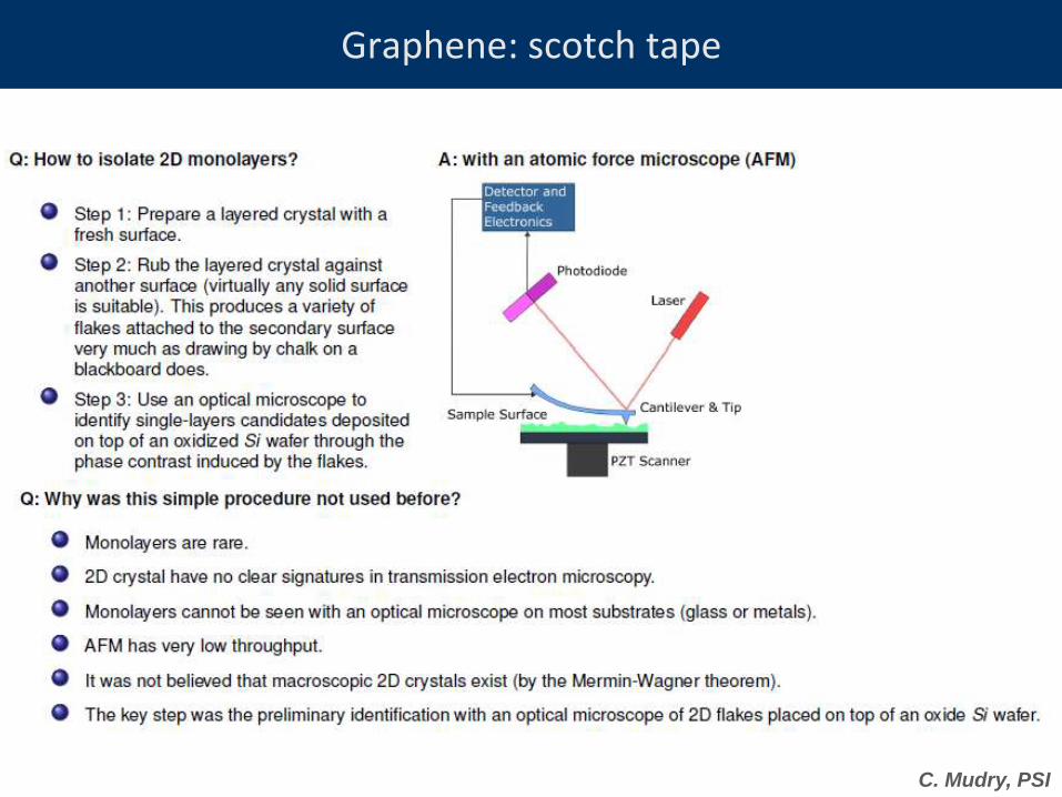
Graphene: scotch tape
J. Trbovic and H. Aurich
2.0µm
970nm
Graphene: scotch tape
C. Mudry, PSI
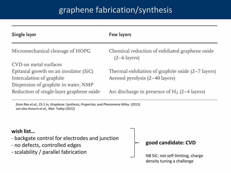
graphene fabrication/synthesis
from Rao et al., Ch.1 in, Graphene: Synthesis, Properties, and Phenomena Wiley (2013) see also Avouris et al., Mat. Today (2012)
wish list… - backgate control for electrodes and junction - no defects, controlled edges - scalability / parallel fabrication
good candidate: CVD
NB SiC: not self-limiting, charge density tuning a challenge
CVD process & catalyst materials
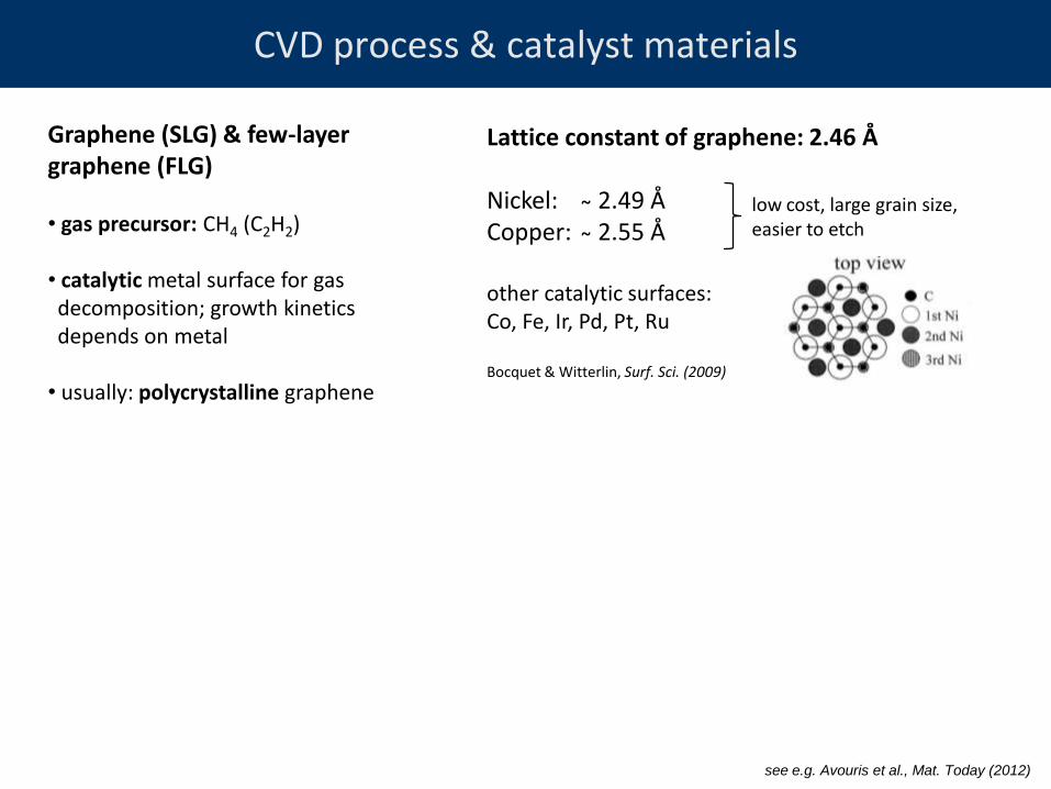
Bocquet & Witterlin, Surf. Sci. (2009)
Lattice constant of graphene: 2.46 Å Nickel: ̴ 2.49 Å Copper: ̴ 2.55 Å other catalytic surfaces: Co, Fe, Ir, Pd, Pt, Ru
low cost, large grain size, easier to etch
see e.g. Avouris et al., Mat. Today (2012)
Graphene (SLG) & few-layer graphene (FLG) • gas precursor: CH4 (C2H2)
• catalytic metal surface for gas decomposition; growth kinetics depends on metal
• usually: polycrystalline graphene
CVD process & catalyst materials
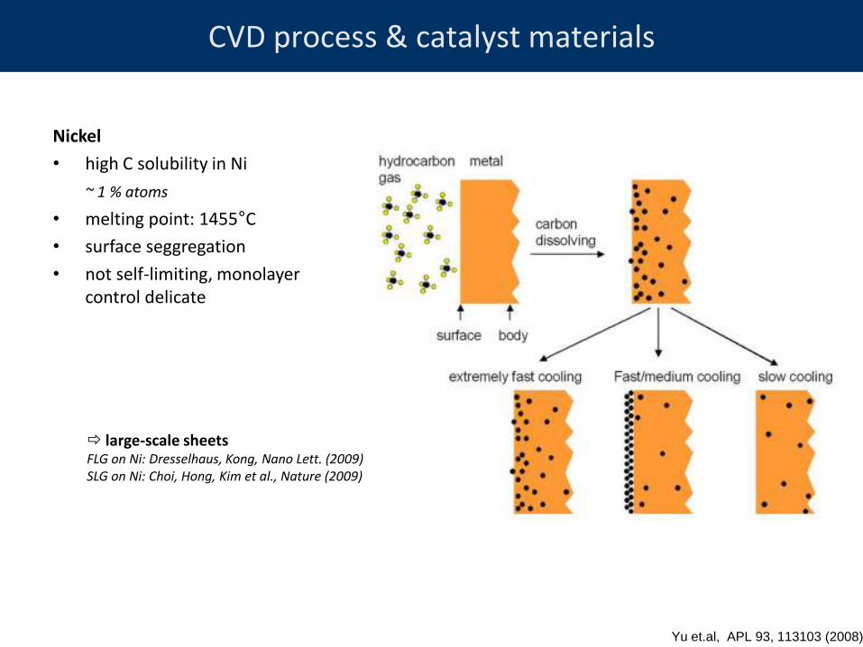
Nickel
• high C solubility in Ni
~ 1 % atoms
• melting point: 1455°C
• surface seggregation
• not self-limiting, monolayer control delicate
Yu et.al, APL 93, 113103 (2008)
large-scale sheets FLG on Ni: Dresselhaus, Kong, Nano Lett. (2009) SLG on Ni: Choi, Hong, Kim et al., Nature (2009)
CVD process & catalyst materials
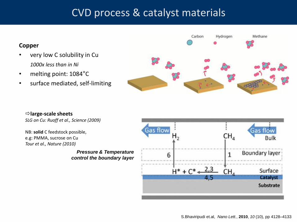
Copper
• very low C solubility in Cu
1000x less than in Ni
• melting point: 1084°C
• surface mediated, self-limiting
large-scale sheets SLG on Cu: Ruoff et al., Science (2009) NB: solid C feedstock possible, e.g: PMMA, sucrose on Cu Tour et al., Nature (2010)
S.Bhaviripudi et.al, Nano Lett., 2010, 10 (10), pp 4128–4133
Pressure & Temperature
control the boundary layer
CVD process & catalyst materials
Bocquet & Witterlin, Surf. Sci. (2009)
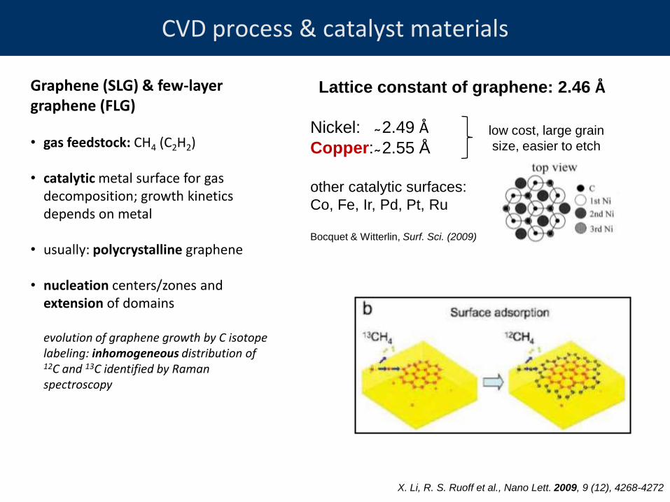
Lattice constant of graphene: 2.46 Å
Nickel: ̴ 2.49 Å
Copper: ̴ 2.55 Å
other catalytic surfaces:
Co, Fe, Ir, Pd, Pt, Ru
low cost, large grain
size, easier to etch
Graphene (SLG) & few-layer graphene (FLG) • gas feedstock: CH4 (C2H2)
• catalytic metal surface for gas decomposition; growth kinetics depends on metal
• usually: polycrystalline graphene
• nucleation centers/zones and extension of domains evolution of graphene growth by C isotope labeling: inhomogeneous distribution of 12C and 13C identified by Raman spectroscopy
X. Li, R. S. Ruoff et al., Nano Lett. 2009, 9 (12), 4268-4272
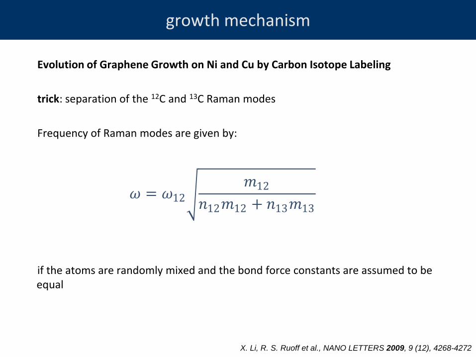
growth mechanism
Evolution of Graphene Growth on Ni and Cu by Carbon Isotope Labeling
trick: separation of the 12C and 13C Raman modes
Frequency of Raman modes are given by:
if the atoms are randomly mixed and the bond force constants are assumed to be equal
X. Li, R. S. Ruoff et al., NANO LETTERS 2009, 9 (12), 4268-4272
𝜔 = 𝜔12 𝑚12
𝑛12𝑚12 + 𝑛13𝑚13
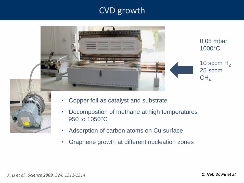
CVD growth
0.05 mbar
1000°C
10 sccm H2
25 sccm
CH4
• Copper foil as catalyst and substrate
• Decompostion of methane at high temperatures
950 to 1050°C
• Adsorption of carbon atoms on Cu surface
• Graphene growth at different nucleation zones
C. Nef, W. Fu et al. X. Li et al., Science 2009, 324, 1312-1314
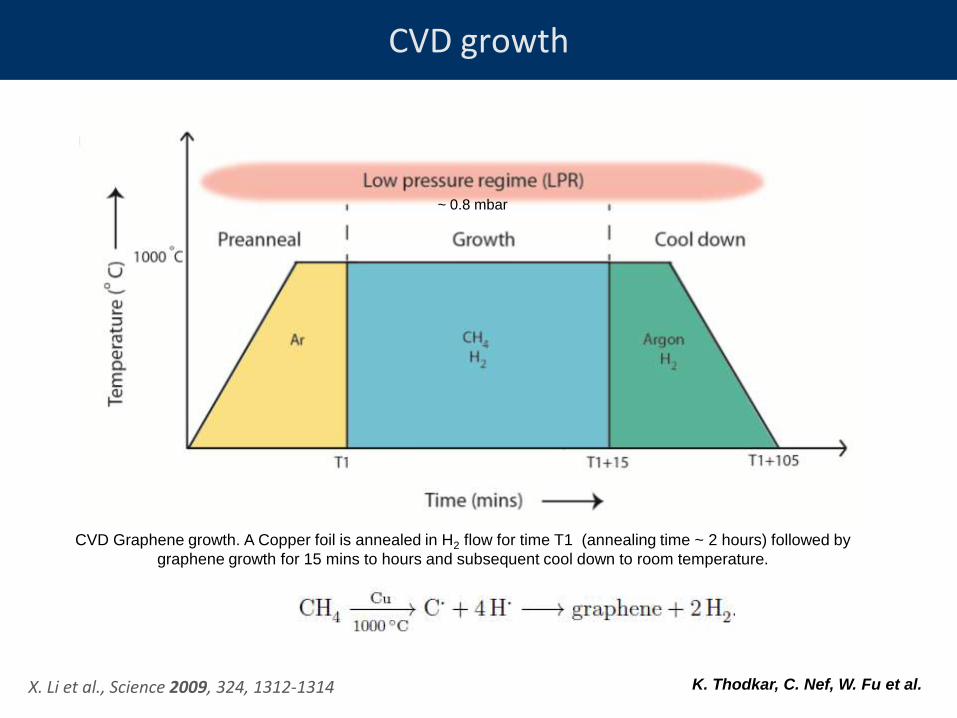
CVD growth
K. Thodkar, C. Nef, W. Fu et al. X. Li et al., Science 2009, 324, 1312-1314
CVD Graphene growth. A Copper foil is annealed in H2 flow for time T1 (annealing time ~ 2 hours) followed by
graphene growth for 15 mins to hours and subsequent cool down to room temperature.
~ 0.8 mbar
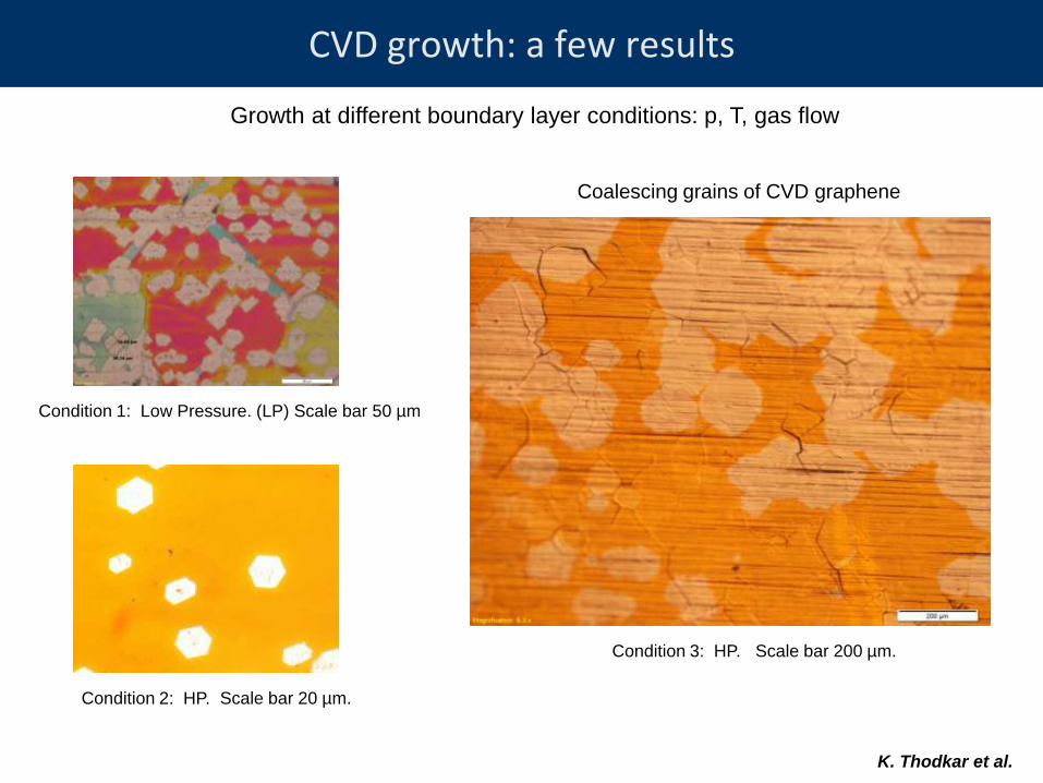
CVD growth: a few results
Condition 1: Low Pressure. (LP) Scale bar 50 µm
Condition 2: HP. Scale bar 20 µm.
Condition 3: HP. Scale bar 200 µm.
Coalescing grains of CVD graphene
Growth at different boundary layer conditions: p, T, gas flow
K. Thodkar et al.
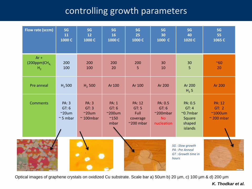
controlling growth parameters
Flow rate (sccm) SG 11
1000 C
SG 12
1000 C
SG 16
1000 C
SG 25
1000 C
SG 30
1000 C
SG 40
1020 C
SG 55
1065 C
Ar + (200ppm)CH4,
H2
200 100
200 100
200 20
200
5
30 10
30 5
~60 20
Pre anneal
H2 500
H2 500
Ar 100
Ar 100
Ar 200
Ar 200
H2 5
Ar 200
Comments
PA: 3 GT: 6
~20um ~ 5 mbar
PA: 3 GT: 3
~20um ~ 100mbar
PA: 1 GT: 6
~200um ~150 mbar
PA: 12 GT: 5 Full
coverage ~200 mbar
PA: 0.5 GT: 6
~200mbar No
nucleation
PA: 0.5 GT: 4
~0.7mbar Square shaped islands
PA: 12 GT: 2
~1000um ~ 200 mbar
SG : Slow growth PA : Pre Anneal GT : Growth time in hours
Optical images of graphene crystals on oxidized Cu substrate. Scale bar a) 50um b) 20 µm, c) 100 µm & d) 200 µm
K. Thodkar et al.
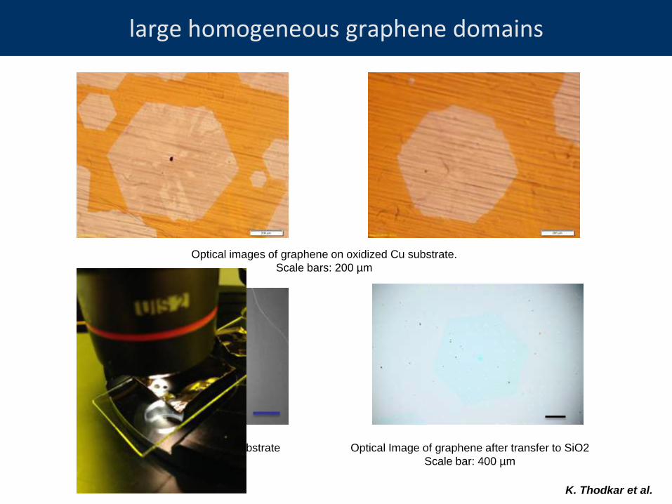
large homogeneous graphene domains
Optical images of graphene on oxidized Cu substrate.
Scale bars: 200 µm
SEM Image of graphene on Cu substrate
Scale bar: 1 mm
Optical Image of graphene after transfer to SiO2
Scale bar: 400 µm
K. Thodkar et al.
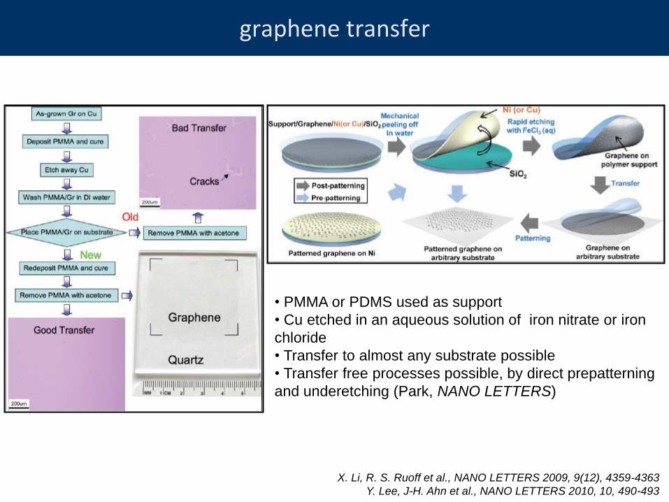
graphene transfer
• PMMA or PDMS used as support
• Cu etched in an aqueous solution of iron nitrate or iron
chloride
• Transfer to almost any substrate possible
• Transfer free processes possible, by direct prepatterning
and underetching (Park, NANO LETTERS)
X. Li, R. S. Ruoff et al., NANO LETTERS 2009, 9(12), 4359-4363
Y. Lee, J-H. Ahn et al., NANO LETTERS 2010, 10, 490-493
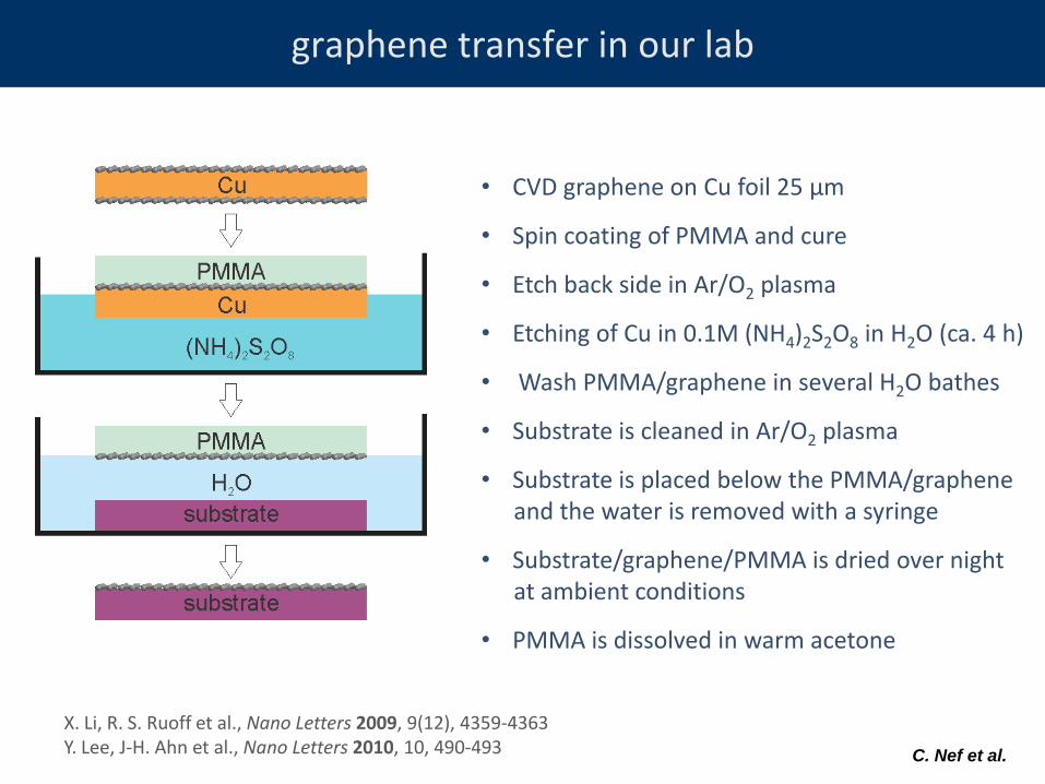
graphene transfer in our lab
• CVD graphene on Cu foil 25 μm
• Spin coating of PMMA and cure
• Etch back side in Ar/O2 plasma
• Etching of Cu in 0.1M (NH4)2S2O8 in H2O (ca. 4 h)
• Wash PMMA/graphene in several H2O bathes
• Substrate is cleaned in Ar/O2 plasma
• Substrate is placed below the PMMA/graphene and the water is removed with a syringe
• Substrate/graphene/PMMA is dried over night at ambient conditions
• PMMA is dissolved in warm acetone
X. Li, R. S. Ruoff et al., Nano Letters 2009, 9(12), 4359-4363 Y. Lee, J-H. Ahn et al., Nano Letters 2010, 10, 490-493 C. Nef et al.
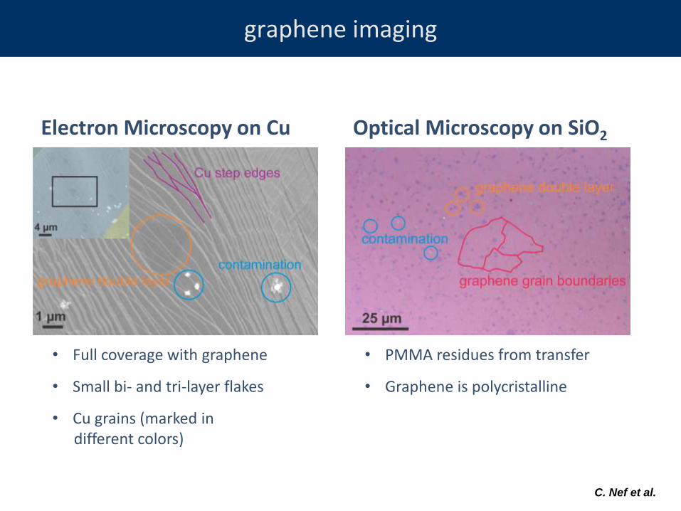
graphene imaging
C. Nef et al.
Electron Microscopy on Cu Optical Microscopy on SiO2
• Full coverage with graphene
• Small bi- and tri-layer flakes
• Cu grains (marked in different colors)
• PMMA residues from transfer
• Graphene is polycristalline
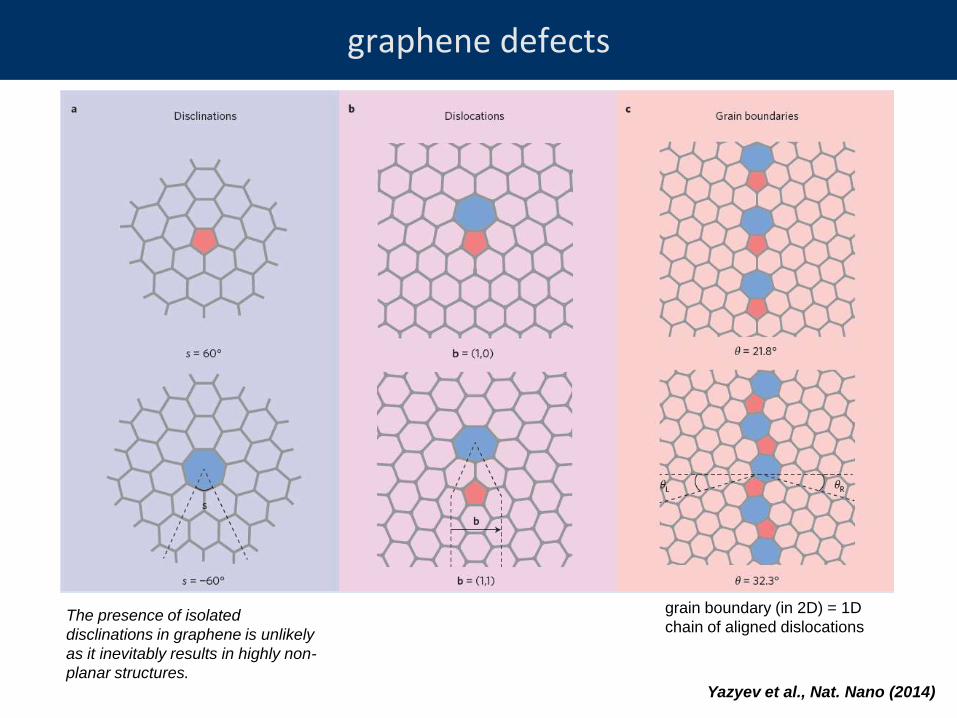
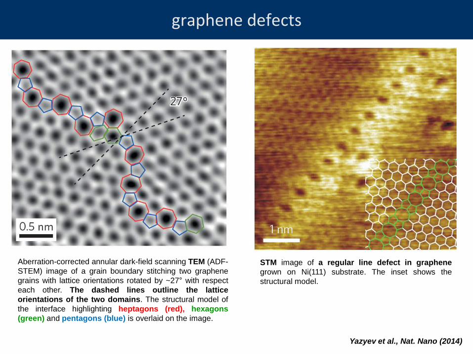
graphene defects
Yazyev et al., Nat. Nano (2014)
The presence of isolated
disclinations in graphene is unlikely
as it inevitably results in highly non-
planar structures.
grain boundary (in 2D) = 1D
chain of aligned dislocations
graphene defects
Yazyev et al., Nat. Nano (2014)
Aberration-corrected annular dark-field scanning TEM (ADF-
STEM) image of a grain boundary stitching two graphene
grains with lattice orientations rotated by ~27° with respect
each other. The dashed lines outline the lattice
orientations of the two domains. The structural model of
the interface highlighting heptagons (red), hexagons
(green) and pentagons (blue) is overlaid on the image.
STM image of a regular line defect in graphene
grown on Ni(111) substrate. The inset shows the
structural model.
• graphene structure
• fabrication and CVD growth
• characterization: Raman spectroscopy
Examples
• graphene electroburning for molecular junctions
• Quantum Hall Effect
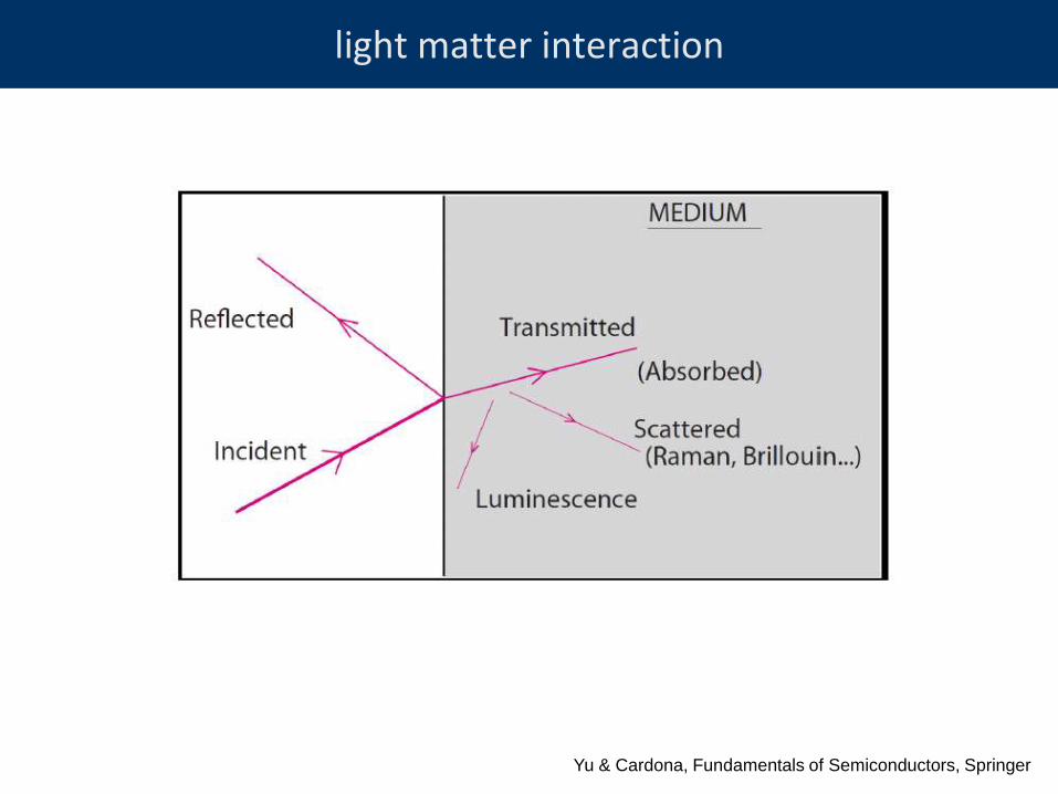
light matter interaction
Yu & Cardona, Fundamentals of Semiconductors, Springer
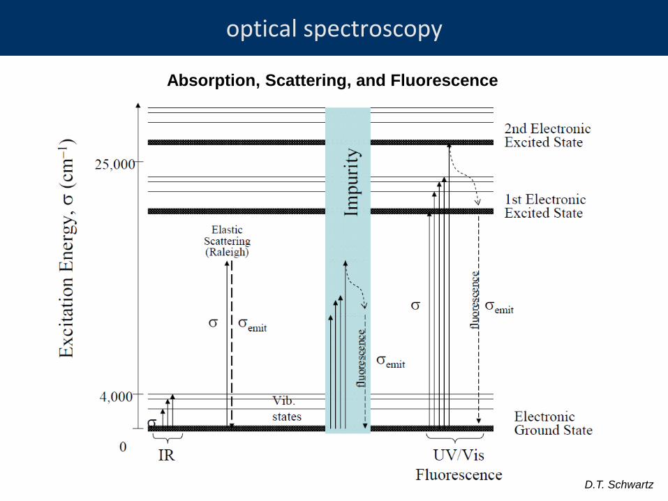
optical spectroscopy
Absorption, Scattering, and Fluorescence
D.T. Schwartz
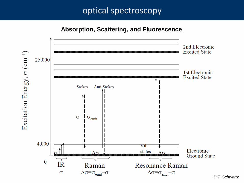
optical spectroscopy
Absorption, Scattering, and Fluorescence
D.T. Schwartz
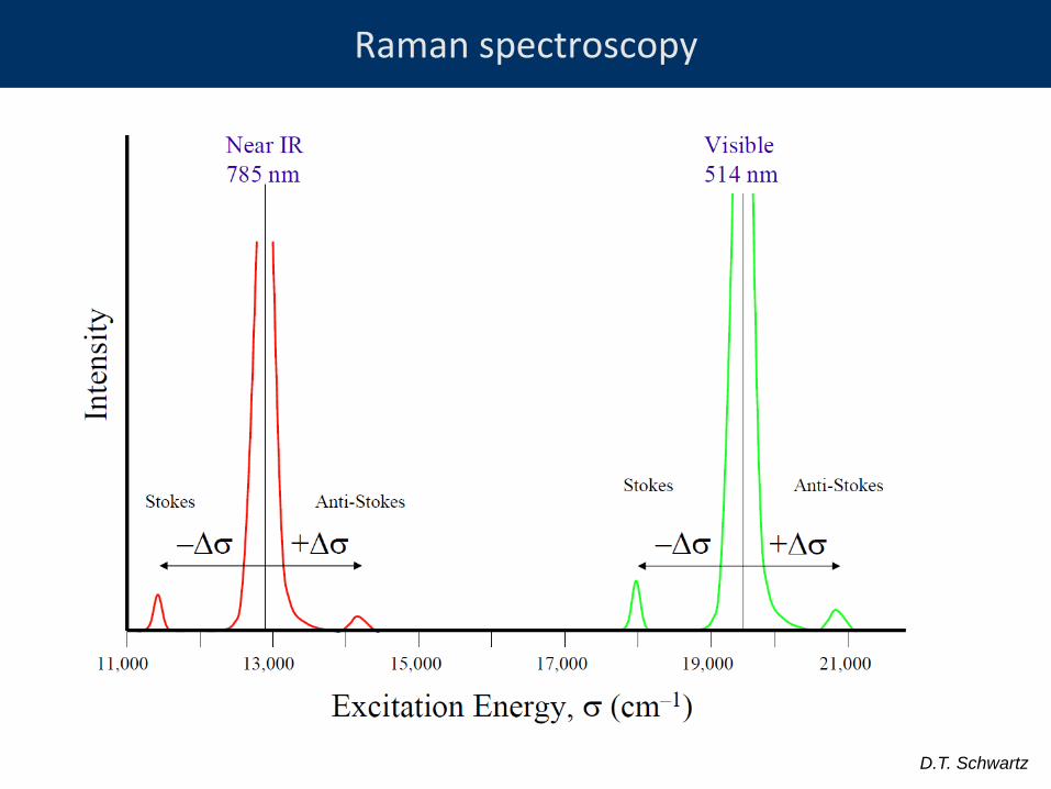
Raman spectroscopy
D.T. Schwartz
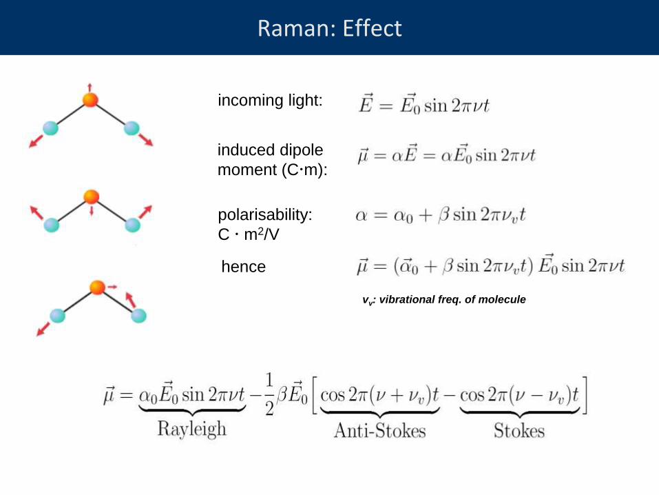
Raman: Effect
incoming light:
induced dipole
moment (Cm):
polarisability:
C m2/V
vv: vibrational freq. of molecule
hence
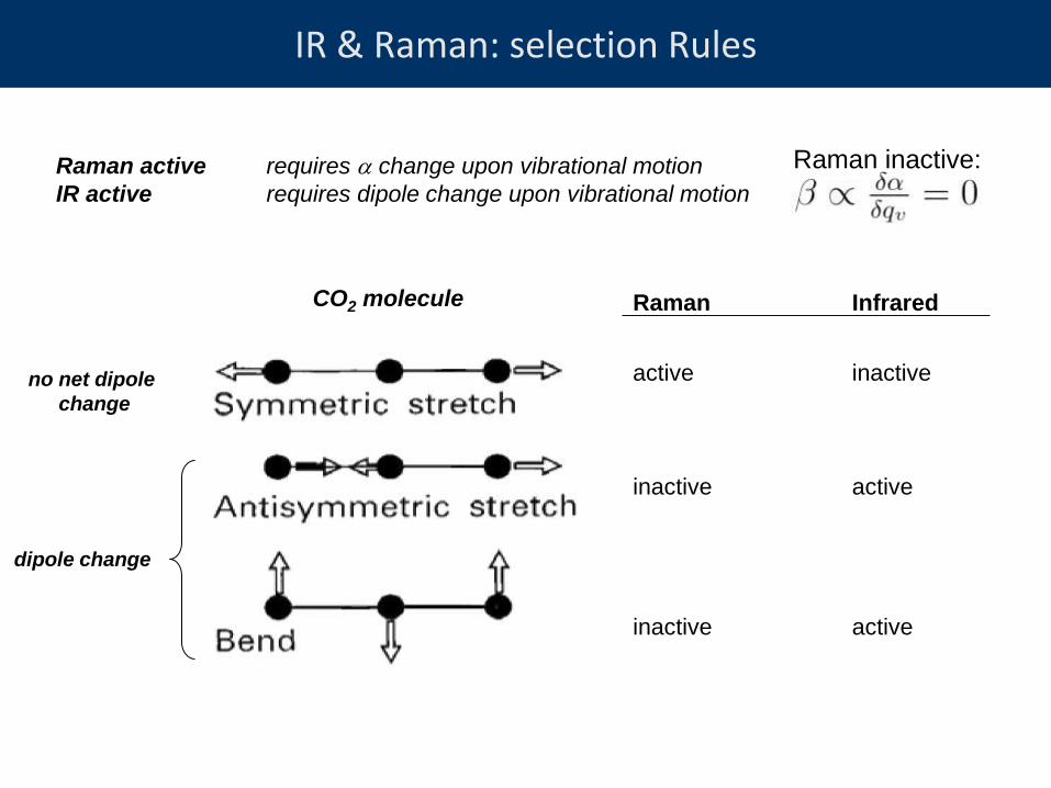
IR & Raman: selection Rules
Raman inactive:
CO2 molecule Raman Infrared
active inactive
inactive active
inactive active
Raman active requires change upon vibrational motion
IR active requires dipole change upon vibrational motion
no net dipole
change
dipole change
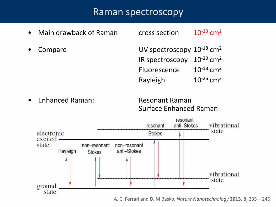
Raman spectroscopy
A. C. Ferrari and D. M Basko, Nature Nanotechnology 2013, 8, 235 – 246
• Main drawback of Raman cross section 10-30 cm2
• Compare UV spectroscopy 10-18 cm2
IR spectroscopy 10-20 cm2
Fluorescence 10-18 cm2
Rayleigh 10-26 cm2
• Enhanced Raman: Resonant Raman Surface Enhanced Raman
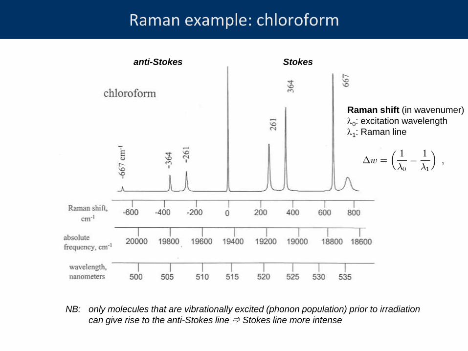
Raman example: chloroform
NB: only molecules that are vibrationally excited (phonon population) prior to irradiation
can give rise to the anti-Stokes line Stokes line more intense
Stokes anti-Stokes
Raman shift (in wavenumer)
l0: excitation wavelength
l1: Raman line
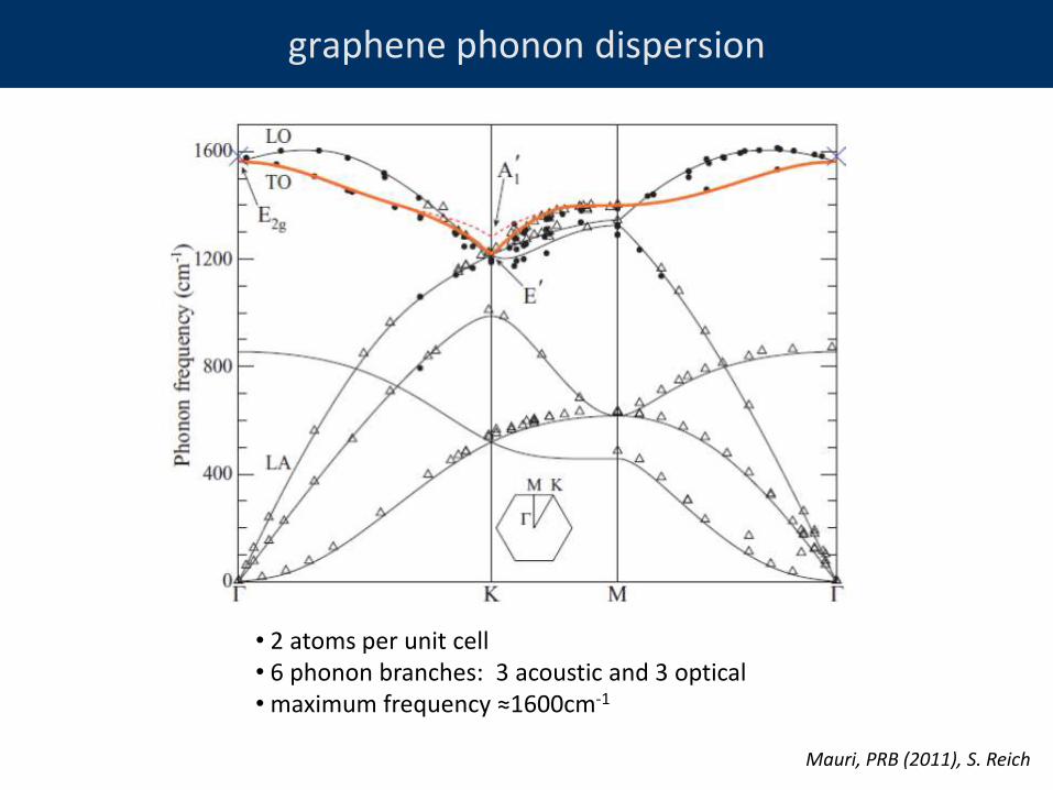
graphene phonon dispersion
Mauri, PRB (2011), S. Reich
• 2 atoms per unit cell • 6 phonon branches: 3 acoustic and 3 optical • maximum frequency ≈1600cm-1
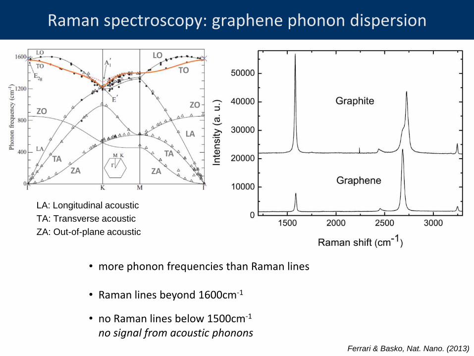
Raman spectroscopy: graphene phonon dispersion
• more phonon frequencies than Raman lines
• Raman lines beyond 1600cm-1
• no Raman lines below 1500cm-1
no signal from acoustic phonons
LA: Longitudinal acoustic
TA: Transverse acoustic
ZA: Out-of-plane acoustic
Ferrari & Basko, Nat. Nano. (2013)
ZA
ZO
TA
LA
TA
ZA
ZO
TO
LO
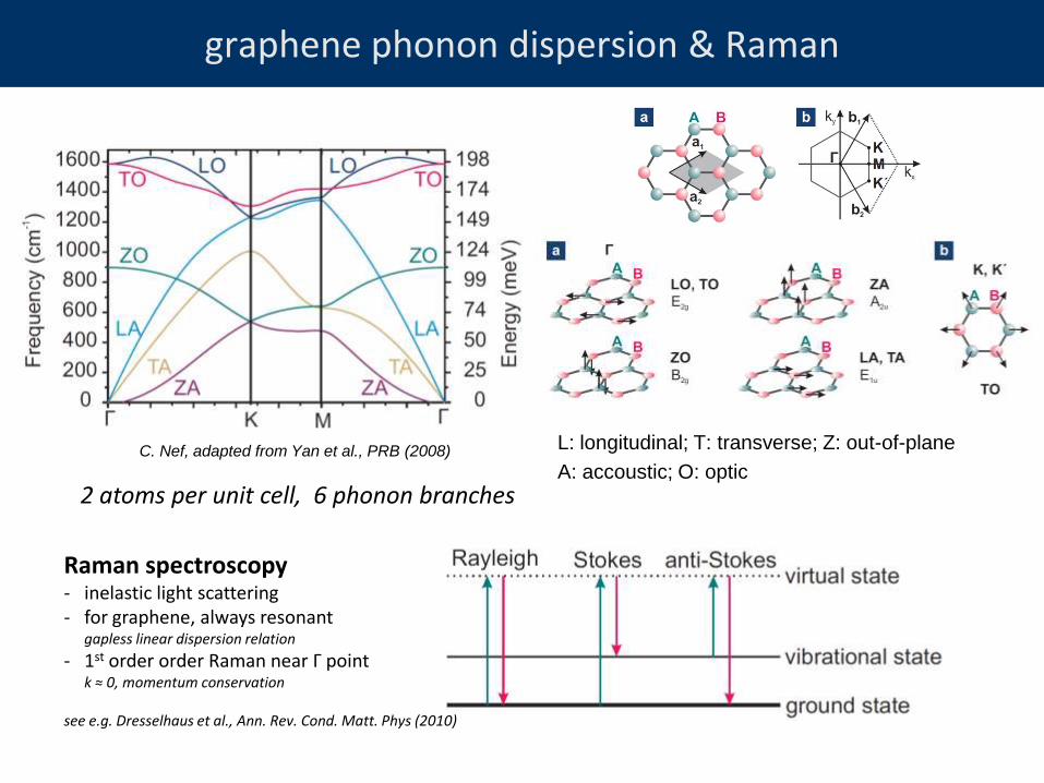
graphene phonon dispersion & Raman
L: longitudinal; T: transverse; Z: out-of-plane
A: accoustic; O: optic C. Nef, adapted from Yan et al., PRB (2008)
2 atoms per unit cell, 6 phonon branches
Raman spectroscopy - inelastic light scattering - for graphene, always resonant gapless linear dispersion relation
- 1st order order Raman near Γ point k ≈ 0, momentum conservation see e.g. Dresselhaus et al., Ann. Rev. Cond. Matt. Phys (2010)
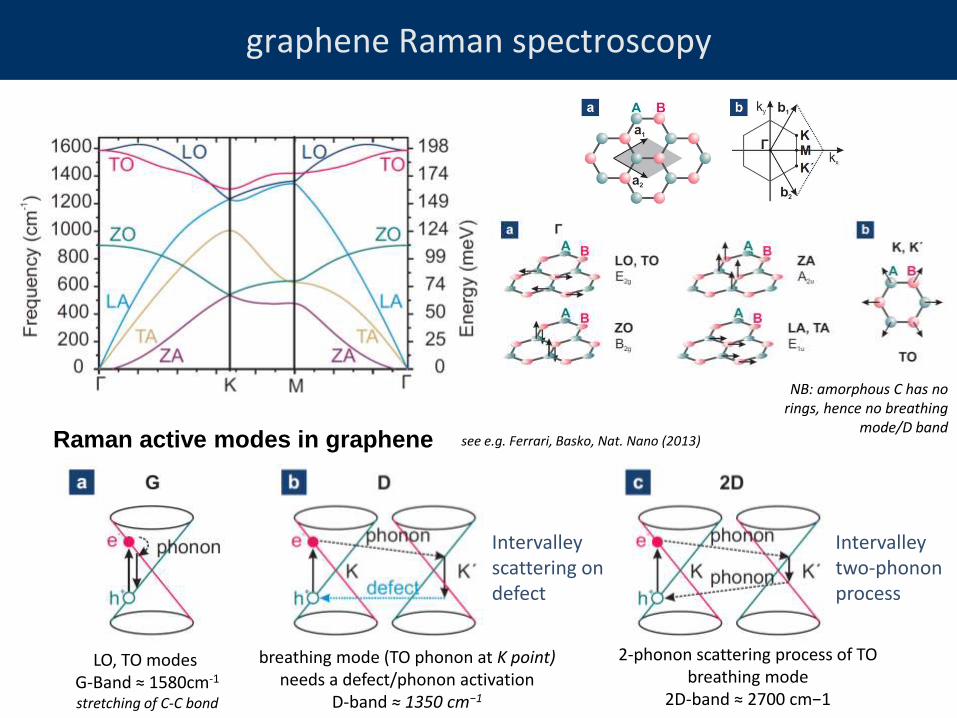
graphene Raman spectroscopy
Raman active modes in graphene see e.g. Ferrari, Basko, Nat. Nano (2013)
LO, TO modes G-Band ≈ 1580cm-1
stretching of C-C bond
breathing mode (TO phonon at K point) needs a defect/phonon activation
D-band ≈ 1350 cm−1
Intervalley scattering on defect
2-phonon scattering process of TO breathing mode
2D-band ≈ 2700 cm−1
Intervalley two-phonon process
NB: amorphous C has no rings, hence no breathing
mode/D band
graphene Raman spectroscopy
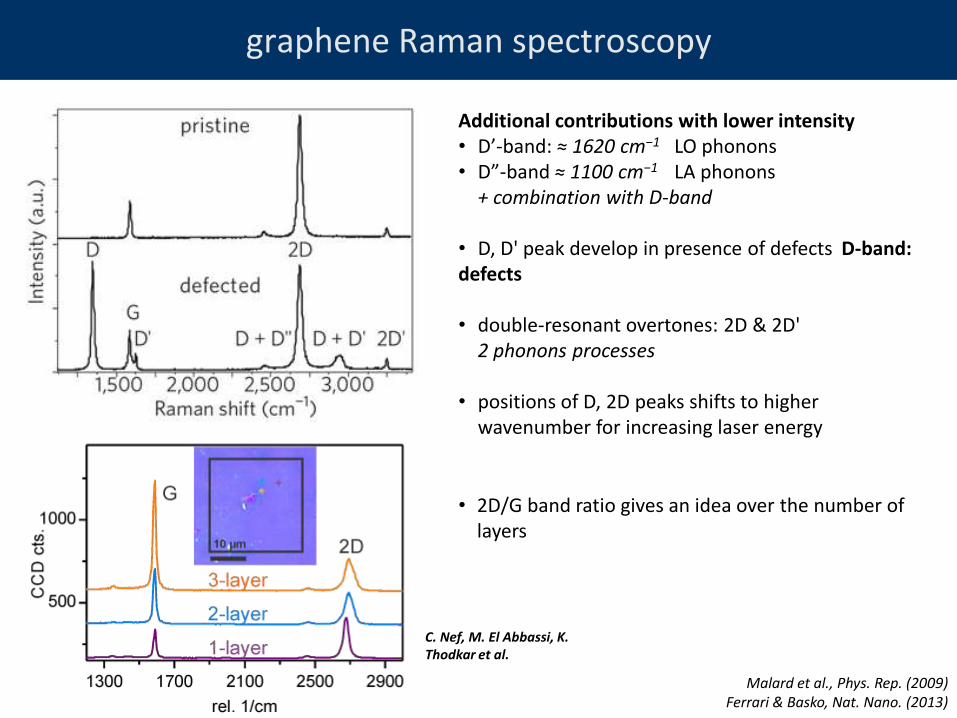
Malard et al., Phys. Rep. (2009) Ferrari & Basko, Nat. Nano. (2013)
Additional contributions with lower intensity • D’-band: ≈ 1620 cm−1 LO phonons • D”-band ≈ 1100 cm−1 LA phonons + combination with D-band
• D, D' peak develop in presence of defects D-band: defects • double-resonant overtones: 2D & 2D' 2 phonons processes • positions of D, 2D peaks shifts to higher wavenumber for increasing laser energy
• 2D/G band ratio gives an idea over the number of layers
C. Nef, M. El Abbassi, K. Thodkar et al.
graphene Raman spectroscopy
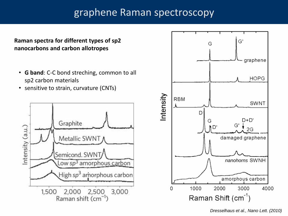
Graphene Raman spectra for different types of sp2 nanocarbons and carbon allotropes
• G band: C-C bond streching, common to all sp2 carbon materials • sensitive to strain, curvature (CNTs)
nanohorns
Dresselhaus et al., Nano Lett. (2010)
Raman spectra
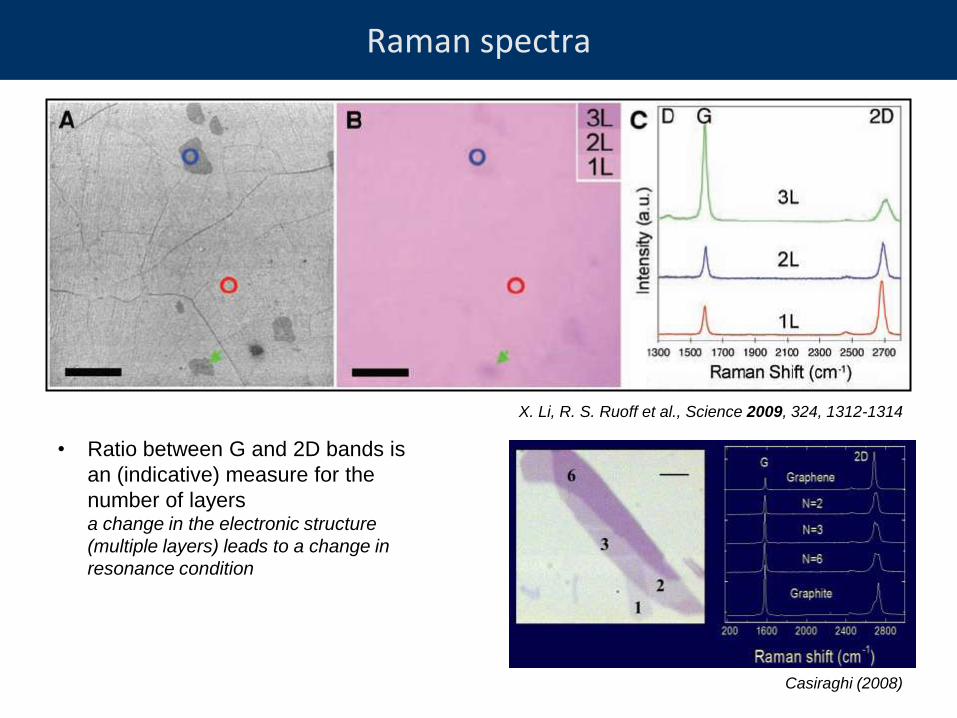
X. Li, R. S. Ruoff et al., Science 2009, 324, 1312-1314
• Ratio between G and 2D bands is
an (indicative) measure for the
number of layers a change in the electronic structure
(multiple layers) leads to a change in
resonance condition
Casiraghi (2008)
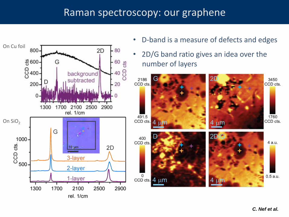
Raman spectroscopy: our graphene
C. Nef et al.
• D-band is a measure of defects and edges
• 2D/G band ratio gives an idea over the number of layers
On Cu foil
On SiO2
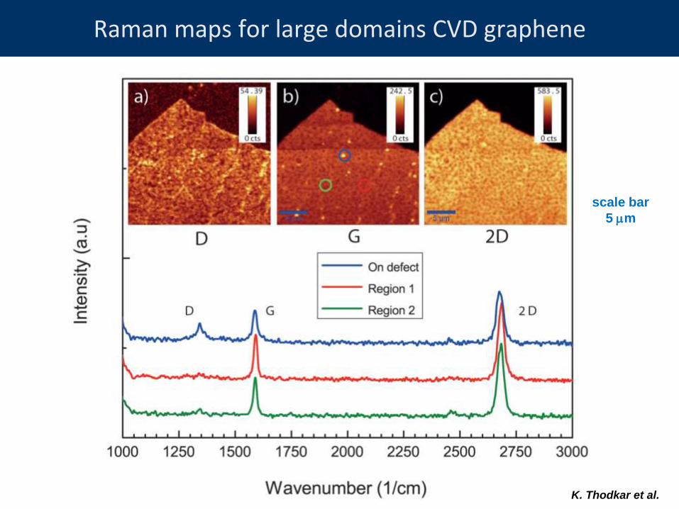
Raman maps for large domains CVD graphene
K. Thodkar et al.
scale bar
5 mm
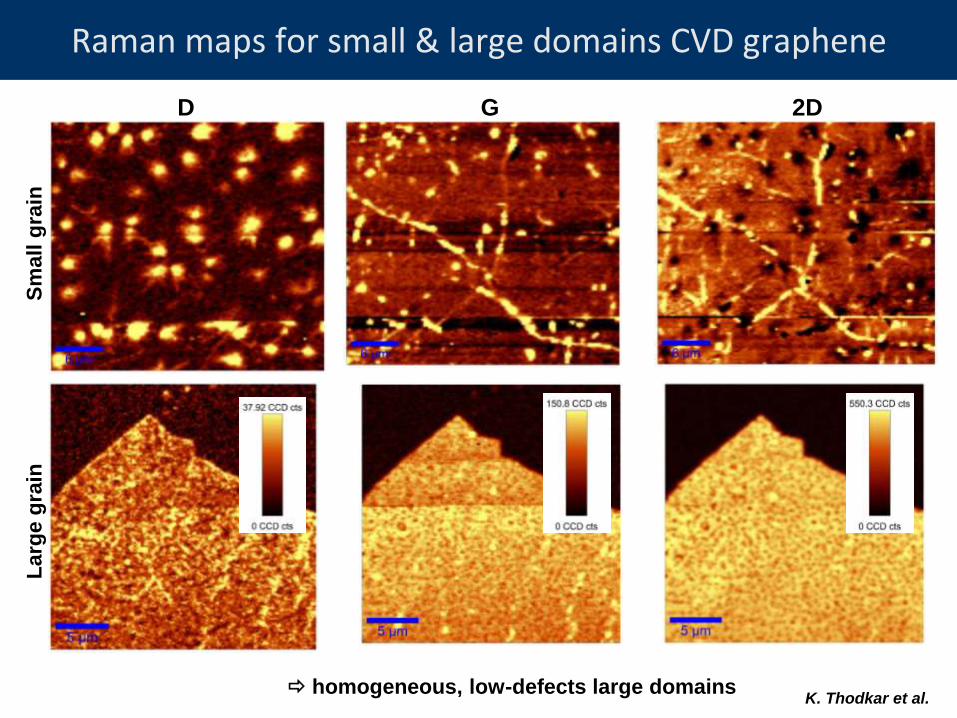
Raman maps for small & large domains CVD graphene
Sm
all g
rain
L
arg
e g
rain
D G 2D
K. Thodkar et al. homogeneous, low-defects large domains
• graphene structure
• fabrication and CVD growth
• characterization: Raman spectroscopy
Examples
• graphene electroburning for molecular junctions
• Quantum Hall Effect
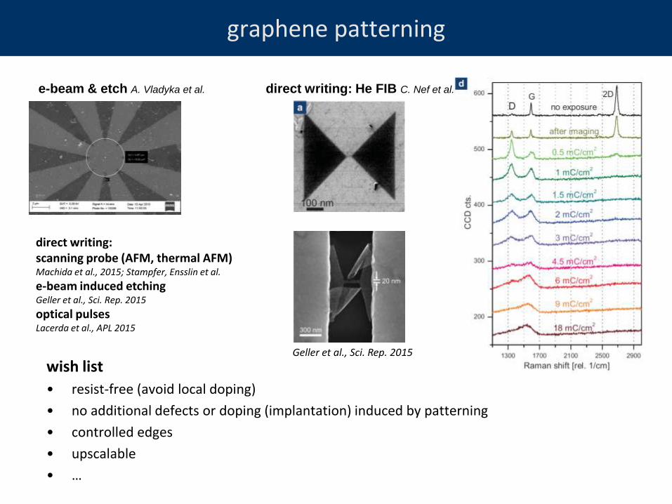
graphene patterning
wish list
• resist-free (avoid local doping)
• no additional defects or doping (implantation) induced by patterning
• controlled edges
• upscalable
• …
e-beam & etch A. Vladyka et al. direct writing: He FIB C. Nef et al.
direct writing: scanning probe (AFM, thermal AFM) Machida et al., 2015; Stampfer, Ensslin et al.
e-beam induced etching Geller et al., Sci. Rep. 2015
optical pulses Lacerda et al., APL 2015
Geller et al., Sci. Rep. 2015
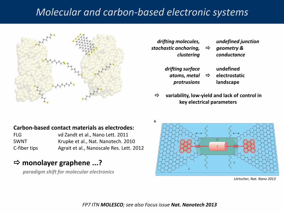
Molecular and carbon-based electronic systems
FP7 ITN MOLESCO; see also Focus issue Nat. Nanotech 2013
paradigm shift for molecular electronics
Carbon-based contact materials as electrodes: FLG vd Zandt et al., Nano Lett. 2011 SWNT Krupke et al., Nat. Nanotech. 2010 C-fiber tips Agrait et al., Nanoscale Res. Lett. 2012
monolayer graphene ...?
Lörtscher, Nat. Nano 2013
drifting molecules, stochastic anchoring,
clustering
undefined junction geometry & conductance
drifting surface atoms, metal
protrusions
undefined electrostatic landscape
variability, low-yield and lack of control in key electrical parameters
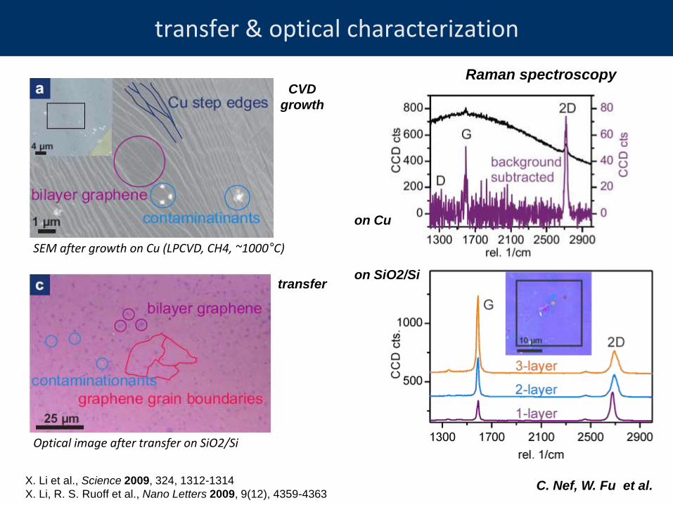
transfer & optical characterization
X. Li et al., Science 2009, 324, 1312-1314
X. Li, R. S. Ruoff et al., Nano Letters 2009, 9(12), 4359-4363 C. Nef, W. Fu et al.
SEM after growth on Cu (LPCVD, CH4, ~1000°C)
Optical image after transfer on SiO2/Si
CVD
growth
transfer
Raman spectroscopy
on Cu
on SiO2/Si
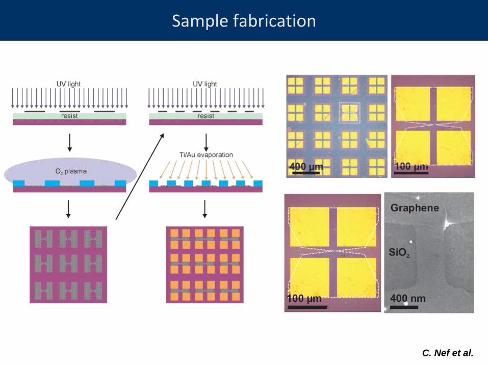
Sample fabrication
C. Nef et al.
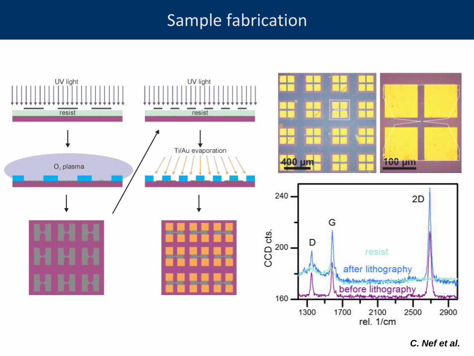
Sample fabrication
C. Nef et al.
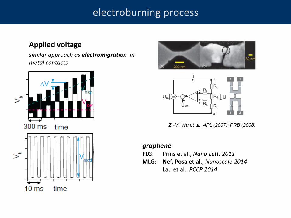
electroburning process
Applied voltage similar approach as electromigration in metal contacts
Z.-M. Wu et al., APL (2007); PRB (2008)
graphene FLG: Prins et al., Nano Lett. 2011 MLG: Nef, Posa et al., Nanoscale 2014 Lau et al., PCCP 2014
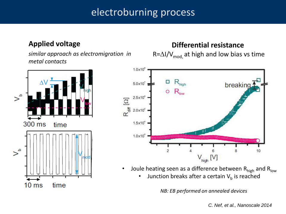
electroburning process
Applied voltage similar approach as electromigration in metal contacts
• Joule heating seen as a difference between Rhigh and Rlow
• Junction breaks after a certain Vb is reached
NB: EB performed on annealed devices
Differential resistance R=DI/Vmod, at high and low bias vs time
C. Nef, et al., Nanoscale 2014
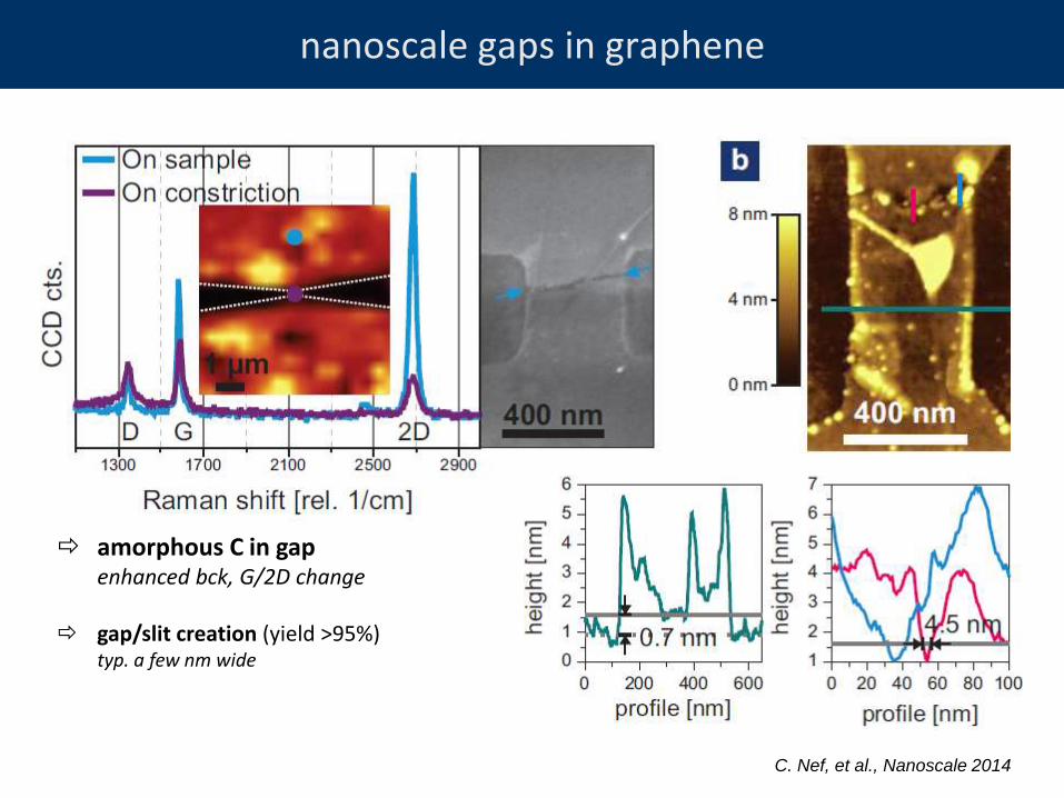
nanoscale gaps in graphene
amorphous C in gap enhanced bck, G/2D change gap/slit creation (yield >95%) typ. a few nm wide
C. Nef, et al., Nanoscale 2014
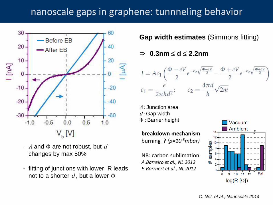
nanoscale gaps in graphene: tunnneling behavior
Gap width estimates (Simmons fitting)
0.3nm d 2.2nm
A : Junction area d : Gap width Φ : Barrier height
- A and Φ are not robust, but d
changes by max 50%
- fitting of junctions with lower R leads
not to a shorter d , but a lower Φ
C. Nef, et al., Nanoscale 2014
breakdown mechanism burning ? (p=10-5mbar) NB: carbon sublimation A.Barreiro et al., NL 2012 F. Börrnert et al., NL 2012
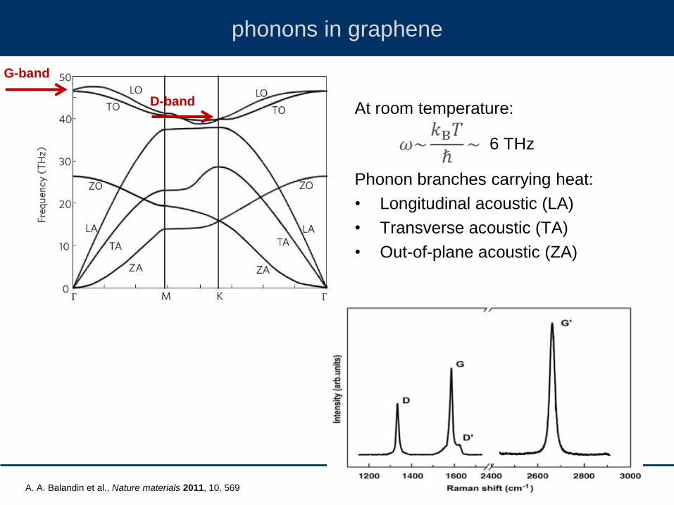
phonons in graphene
At room temperature:
6 THz
Phonon branches carrying heat:
• Longitudinal acoustic (LA)
• Transverse acoustic (TA)
• Out-of-plane acoustic (ZA)
G-band
D-band
A. A. Balandin et al., Nature materials 2011, 10, 569
temperature calibration
Raman peak shift as thermometer - increasing T leads to softening of phonon modes
NB: 2D peak (Intervalley 2-phonon process) shift
more marked, see e.g. Balandin et al., APL 2007
shifts for Si (520 cm-1), D & 2D peaks NB: G peak and FWHM peaks depend on carrier
concentration n and n=n(T)
2D peak shift -0.051 cm-1K-1
Si: inelatic phonon scattering model
D 2D
Si
calibration of Raman peaks shift (heating stage)
C. Nef, et al., Nanoscale 2014
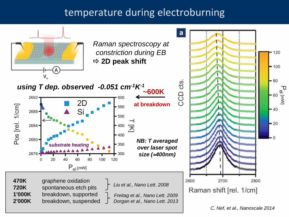
temperature during electroburning
Raman spectroscopy at
constriction during EB
2D peak shift
using T dep. observed -0.051 cm-1K-1 ~600K
at breakdown
470K graphene oxidation
720K spontaneous etch pits
1'000K breakdown, supported
2'000K breakdown, suspended
Liu et al., Nano Lett. 2008
Freitag et al., Nano Lett. 2009
Dorgan et al., Nano Lett. 2013
NB: T averaged
over laser spot
size (400nm)
substrate heating
C. Nef, et al., Nanoscale 2014
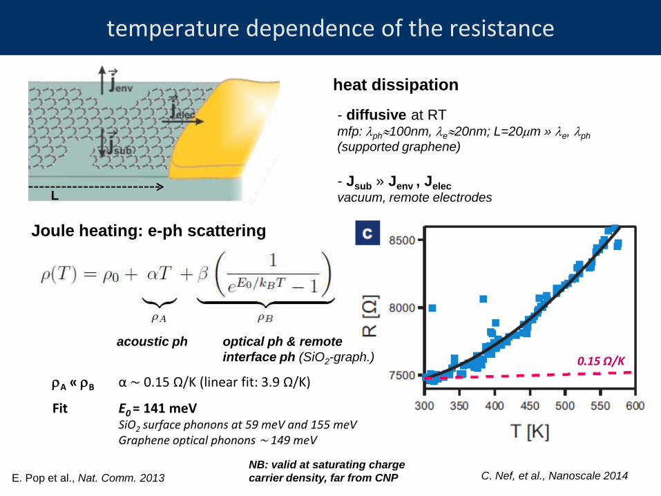
temperature dependence of the resistance
E. Pop et al., Nat. Comm. 2013
heat dissipation
- diffusive at RT mfp: lph100nm, le20nm; L=20mm » le, lph
(supported graphene)
- Jsub » Jenv , Jelec
vacuum, remote electrodes L
Joule heating: e-ph scattering
optical ph & remote
interface ph (SiO2-graph.)
acoustic ph
rA « rB α ∼ 0.15 Ω/K (linear fit: 3.9 Ω/K)
0.15 Ω/K
Fit E0 = 141 meV SiO2 surface phonons at 59 meV and 155 meV Graphene optical phonons ∼ 149 meV
NB: valid at saturating charge
carrier density, far from CNP C. Nef, et al., Nanoscale 2014
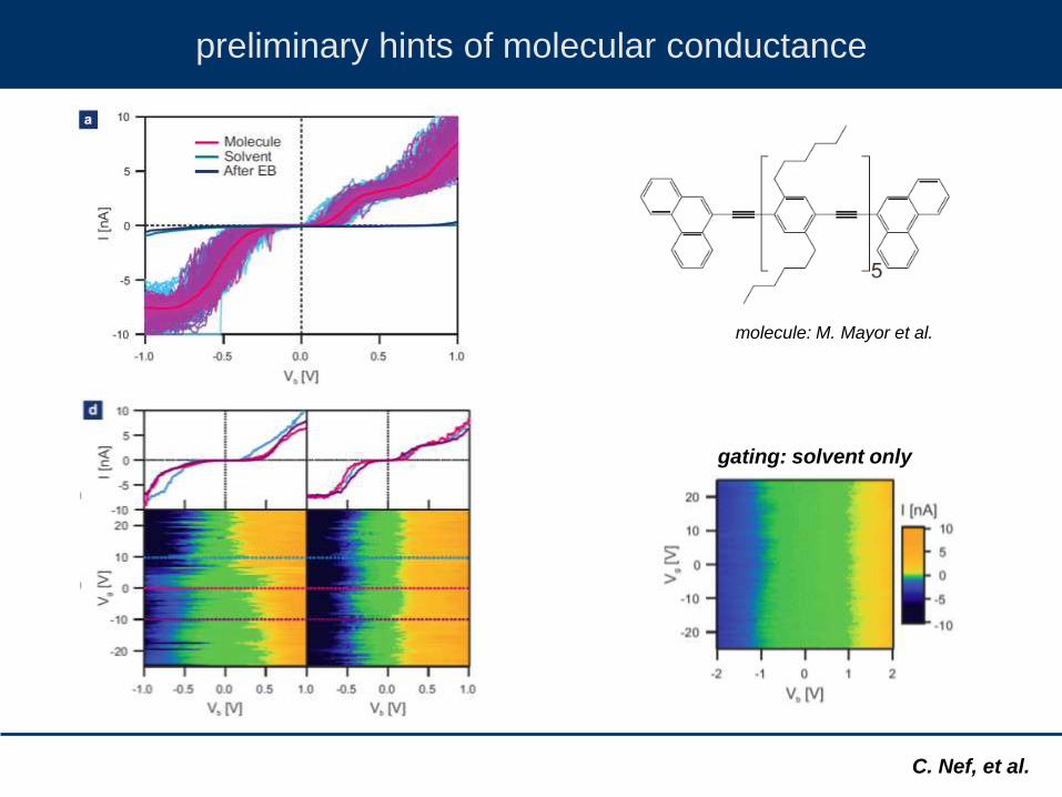
preliminary hints of molecular conductance
C. Nef, et al.
molecule: M. Mayor et al.
gating: solvent only
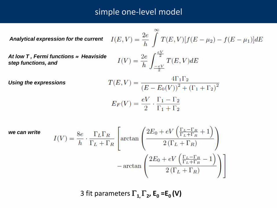
simple one-level model
Analytical expression for the current
3 fit parameters G1, G2, E0 =E0 (V)
we can write
Using the expressions
At low T , Fermi functions Heaviside
step functions, and

preliminary hints of molecular conductance
C. Nef, et al.
qualitative behavior using
simple 1 level model including CB and level broadening
(Datta et al. Nanotech. 2004)
• graphene structure
• fabrication and CVD growth
• characterization: Raman spectroscopy
Examples
• graphene electroburning for molecular
junctions
• Quantum Hall Effect
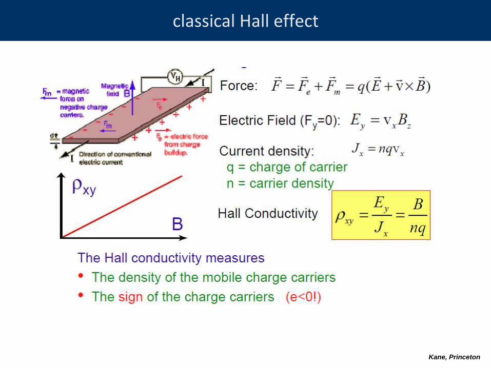
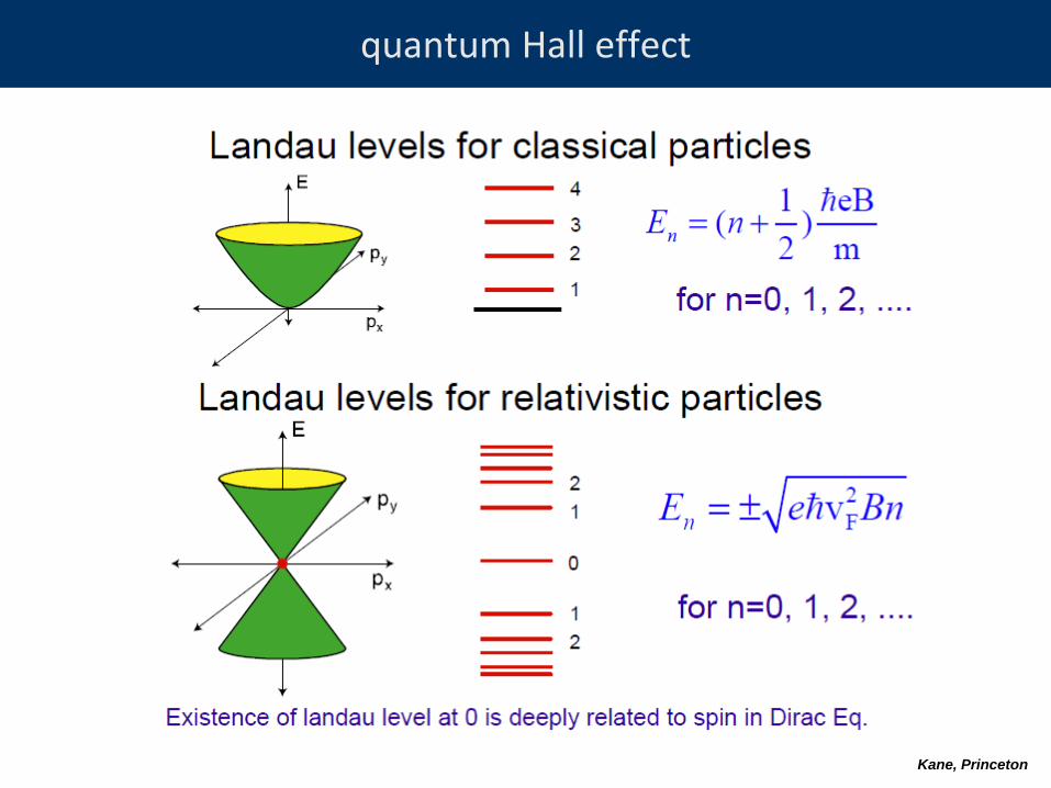
classical Hall effect
Kane, Princeton
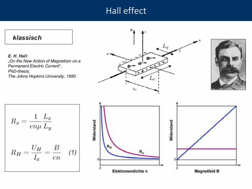
Hall effect
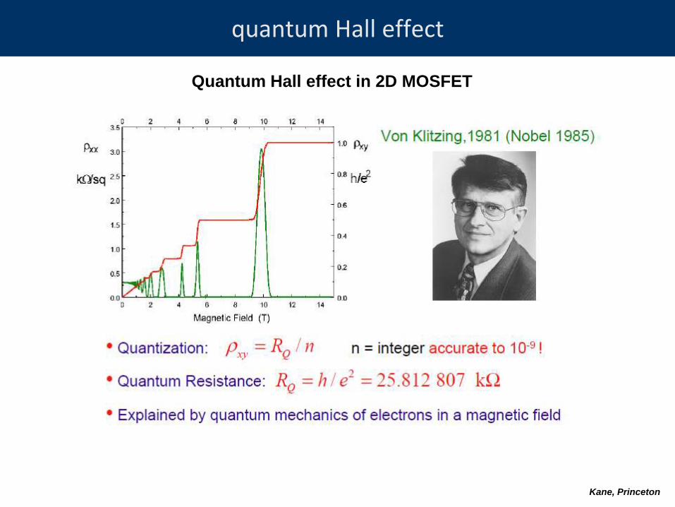
quantum Hall effect
Quantum Hall effect in 2D MOSFET
Kane, Princeton
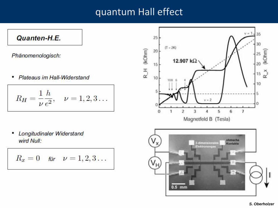
quantum Hall effect
S. Oberholzer
quantum Hall effect
S. Oberholzer, mc
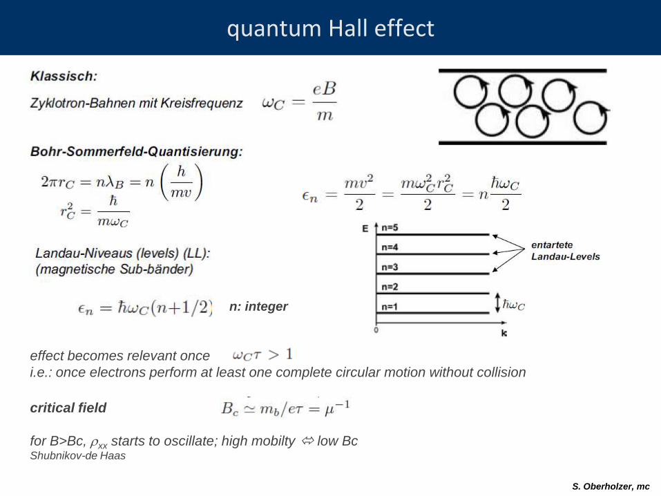
effect becomes relevant once
i.e.: once electrons perform at least one complete circular motion without collision
n: integer
critical field
for B>Bc, rxx starts to oscillate; high mobilty low Bc Shubnikov-de Haas
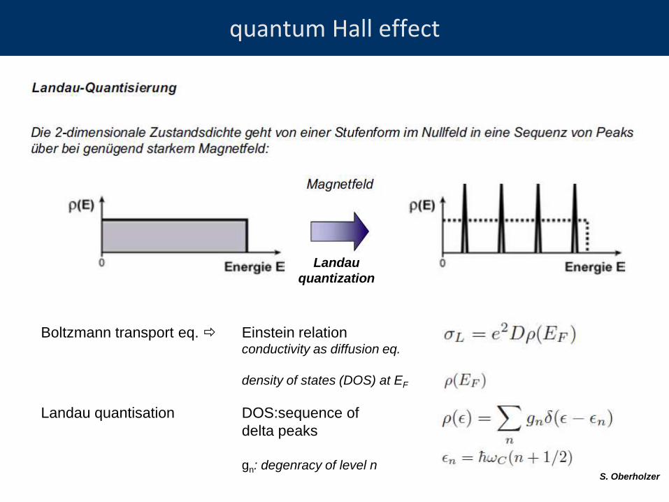
quantum Hall effect
S. Oberholzer
Landau
quantization
Boltzmann transport eq. Einstein relation conductivity as diffusion eq.
density of states (DOS) at EF
Landau quantisation DOS:sequence of
delta peaks
gn: degenracy of level n
quantum Hall effect
Kane, Princeton
quantum Hall effect
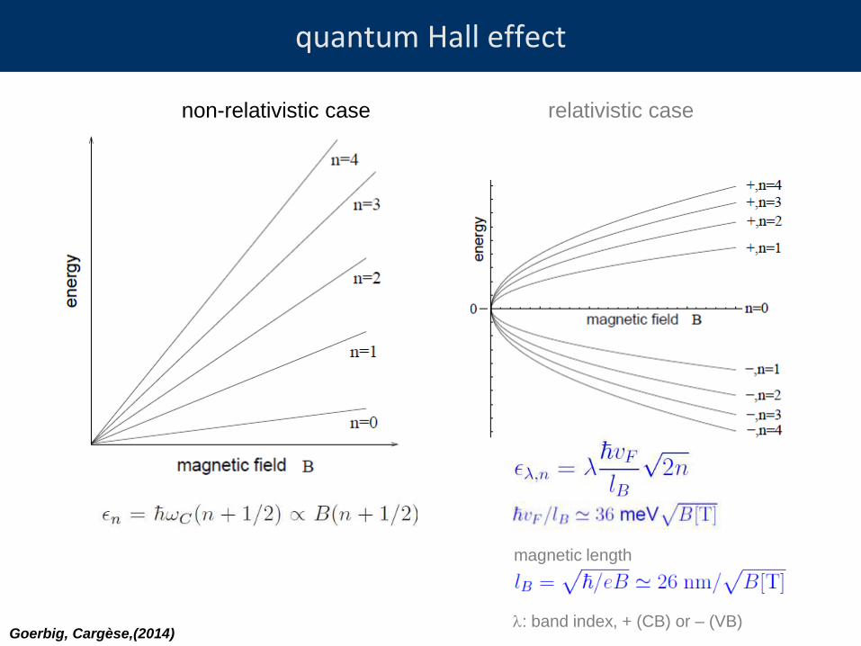
Goerbig, Cargèse,(2014)
non-relativistic case relativistic case
magnetic length
l: band index, + (CB) or – (VB)
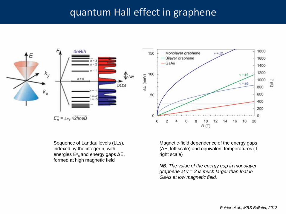
quantum Hall effect in graphene
Poirier et al., MRS Bulletin, 2012
Sequence of Landau levels (LLs),
indexed by the integer n, with
energies E±n and energy gaps ΔE,
formed at high magnetic field
Magnetic-field dependence of the energy gaps
(ΔE, left scale) and equivalent temperatures (T,
right scale)
NB: The value of the energy gap in monolayer
graphene at ν = 2 is much larger than that in
GaAs at low magnetic field.
QHE graphene
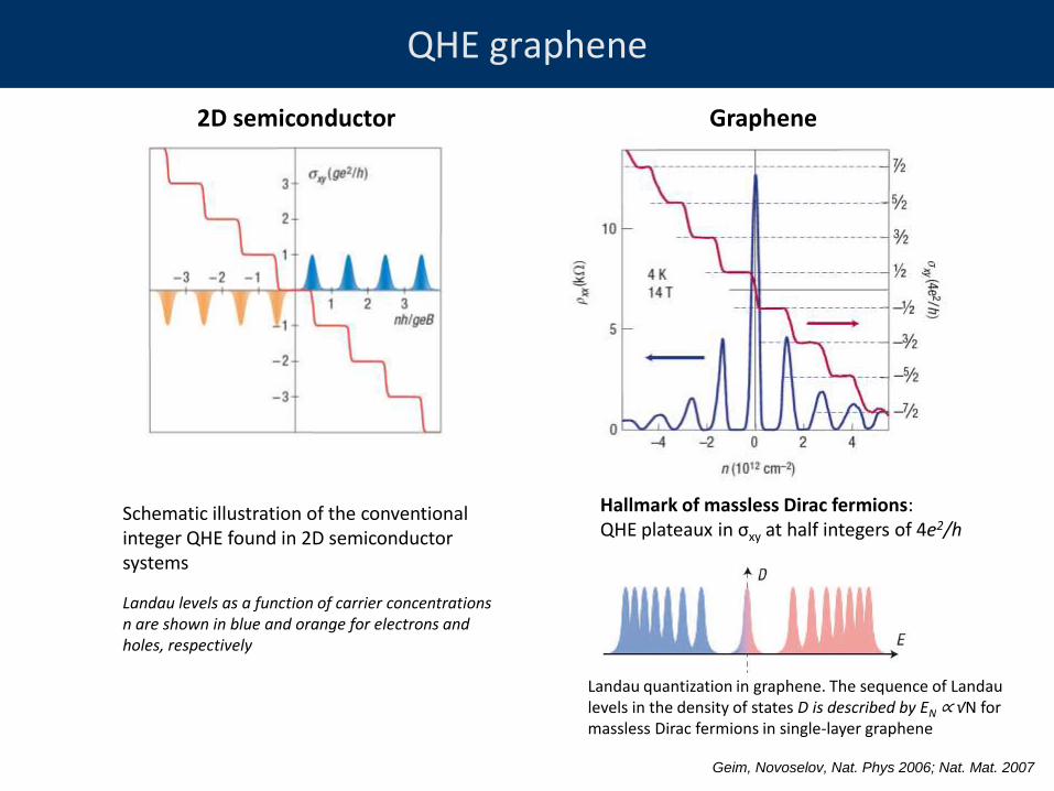
Geim, Novoselov, Nat. Phys 2006; Nat. Mat. 2007
Landau quantization in graphene. The sequence of Landau levels in the density of states D is described by EN ∝ √N for massless Dirac fermions in single-layer graphene
Hallmark of massless Dirac fermions: QHE plateaux in σxy at half integers of 4e2/h
Graphene 2D semiconductor
Schematic illustration of the conventional integer QHE found in 2D semiconductor systems
Landau levels as a function of carrier concentrations n are shown in blue and orange for electrons and holes, respectively

QHE graphene
Geim, Novoselov, Nat. Phys 2006; Nat. Mat. 2007
Landau quantization in graphene. The sequence of Landau levels in the density of states D is described by EN ∝ √N for massless Dirac fermions in single-layer graphene
Hallmark of massless Dirac fermions: QHE plateaux in σxy at half integers of 4e2/h
Graphene 2D semiconductor
Schematic illustration of the conventional integer QHE found in 2D semiconductor systems
Landau levels as a function of carrier concentrations n are shown in blue and orange for electrons and holes, respectively
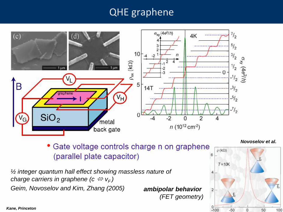
QHE graphene
Novoselov et al.
ambipolar behavior
(FET geometry)
Kane, Princeton
½ integer quantum hall effect showing massless nature of
charge carriers in graphene (c vF )
Geim, Novoselov and Kim, Zhang (2005)