Embed Size (px)
Citation preview
1
Lecture 7: Caching in Row-Buffer of DRAM
Adapted from “A Permutation-based Page Interleaving Scheme: To Reduce Row-buffer Conflicts and Exploit Data Locality” by x. Zhang et. al.
2
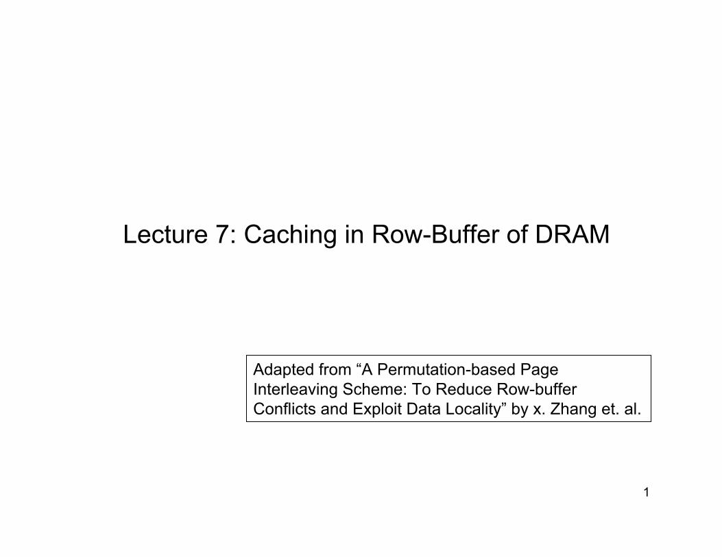
CPU Registers
L1TLB
L3
L2
Row buffer
DRAMBus adapterController
buffer
Buffer cache
CPU-memory bus
I/O bus
I/O controller
disk
Disk cache
TLB
registers
L1
L2
L3
Controller buffer
Buffer cache
disk cache
Row buffer
A Bigger Picture

3
DRAM Architecture
CPU/CacheCPU/Cache
Bus
DRAMDRAM
DRAM
Bank 0 Bank 1 Bank n
CoreCore Core Core
Row buffer
4
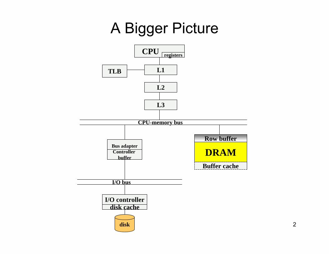
Caching in DRAMDRAM is the center of memory hierarchy:– High density and high capacity– Low cost but slow access (compared to SRAM)
• A cache miss has been considered as a constant delay for long time. This is wrong.– Non-uniform access latencies exist within DRAM
Row-buffer serves as a fast cache in DRAM– Its access patterns here have been paid little
attention. – Reusing buffer data minimizes the DRAM latency.
5
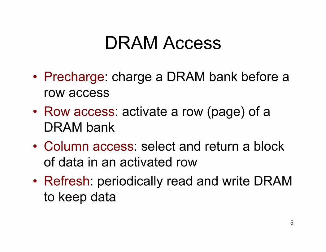
DRAM Access
• Precharge: charge a DRAM bank before a row access
• Row access: activate a row (page) of a DRAM bank
• Column access: select and return a block of data in an activated row
• Refresh: periodically read and write DRAM to keep data
6
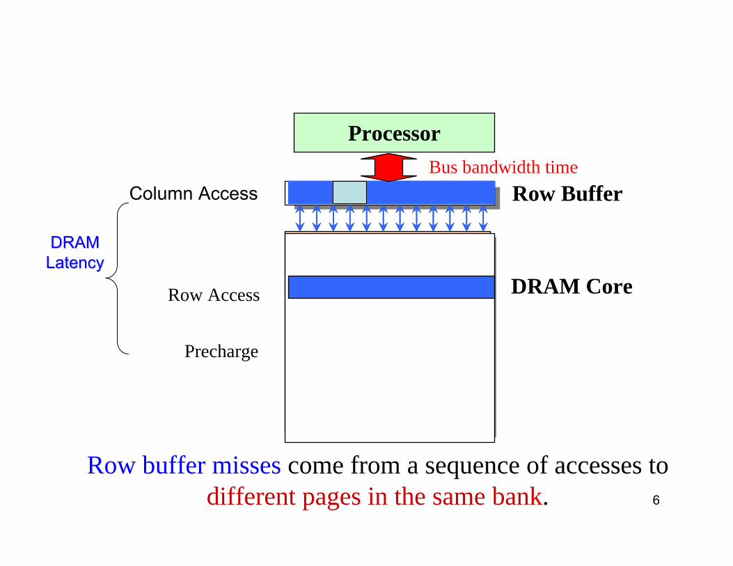
Precharge
Row Access
Bus bandwidth time
DRAM Core
Row Buffer
Processor
Column Access
DRAMDRAMLatencyLatency
Row buffer misses come from a sequence of accesses to different pages in the same bank.
7
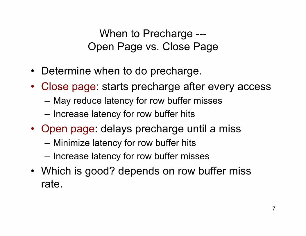
When to Precharge ---Open Page vs. Close Page
• Determine when to do precharge.• Close page: starts precharge after every access
– May reduce latency for row buffer misses– Increase latency for row buffer hits
• Open page: delays precharge until a miss– Minimize latency for row buffer hits– Increase latency for row buffer misses
• Which is good? depends on row buffer miss rate.
8
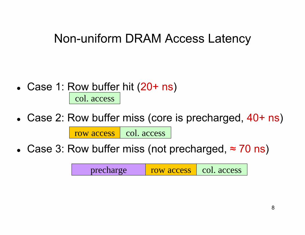
Non-uniform DRAM Access Latency
Case 1: Row buffer hit (20+ ns)
Case 2: Row buffer miss (core is precharged, 40+ ns)
Case 3: Row buffer miss (not precharged, ≈ 70 ns)
precharge row access col. access
row access col. access
col. access

9
Amdahl’s Law applies in DRAM
70
70
20
60
16070
6.4GB/s(Rambus)
2.1GB/s(PC2100)
0.8GB/s(PC100)
♦As the bandwidth improves, DRAM latency will decide cache miss penalty.
♦Time (ns) to fetch a 128-byte cache block:latency bandwidth
10
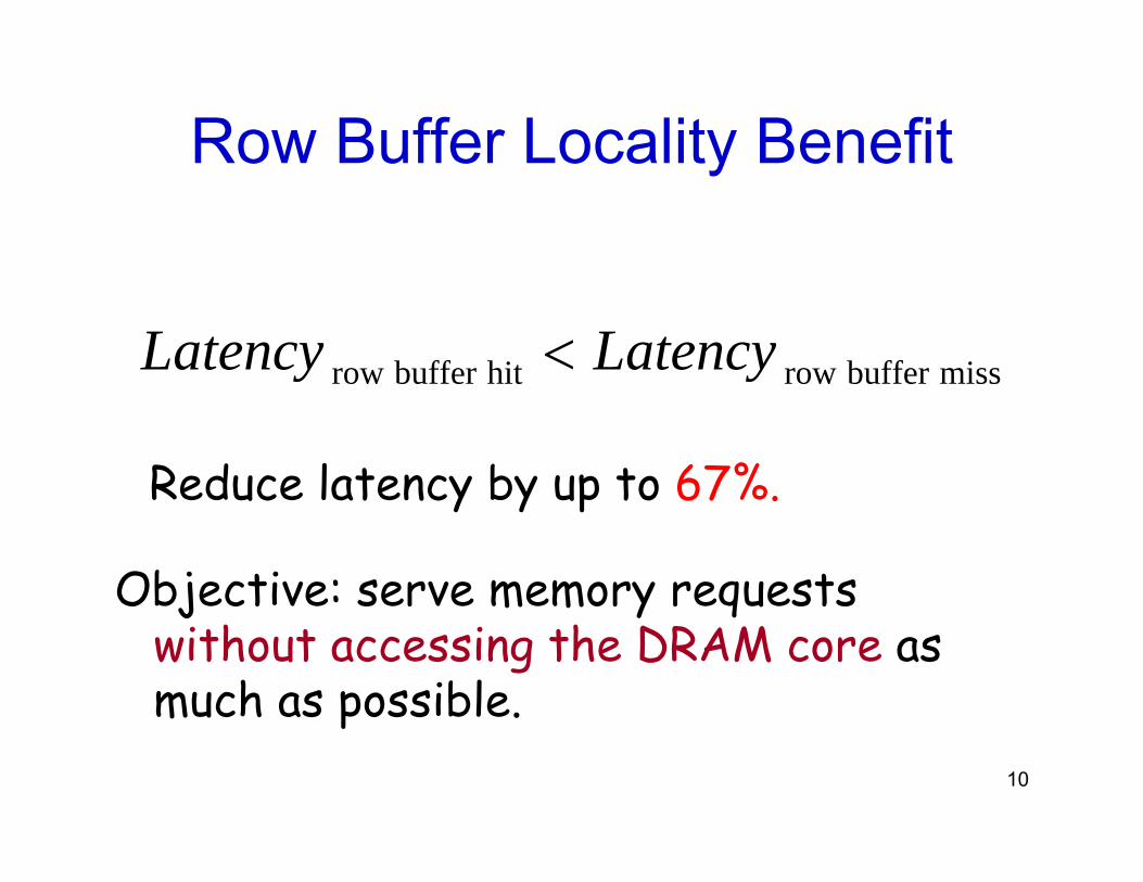
Row Buffer Locality Benefit
Objective: serve memory requests without accessing the DRAM core as much as possible.
missbuffer rowhitbuffer row LatencyLatency <
Reduce latency by up to 67%.
11
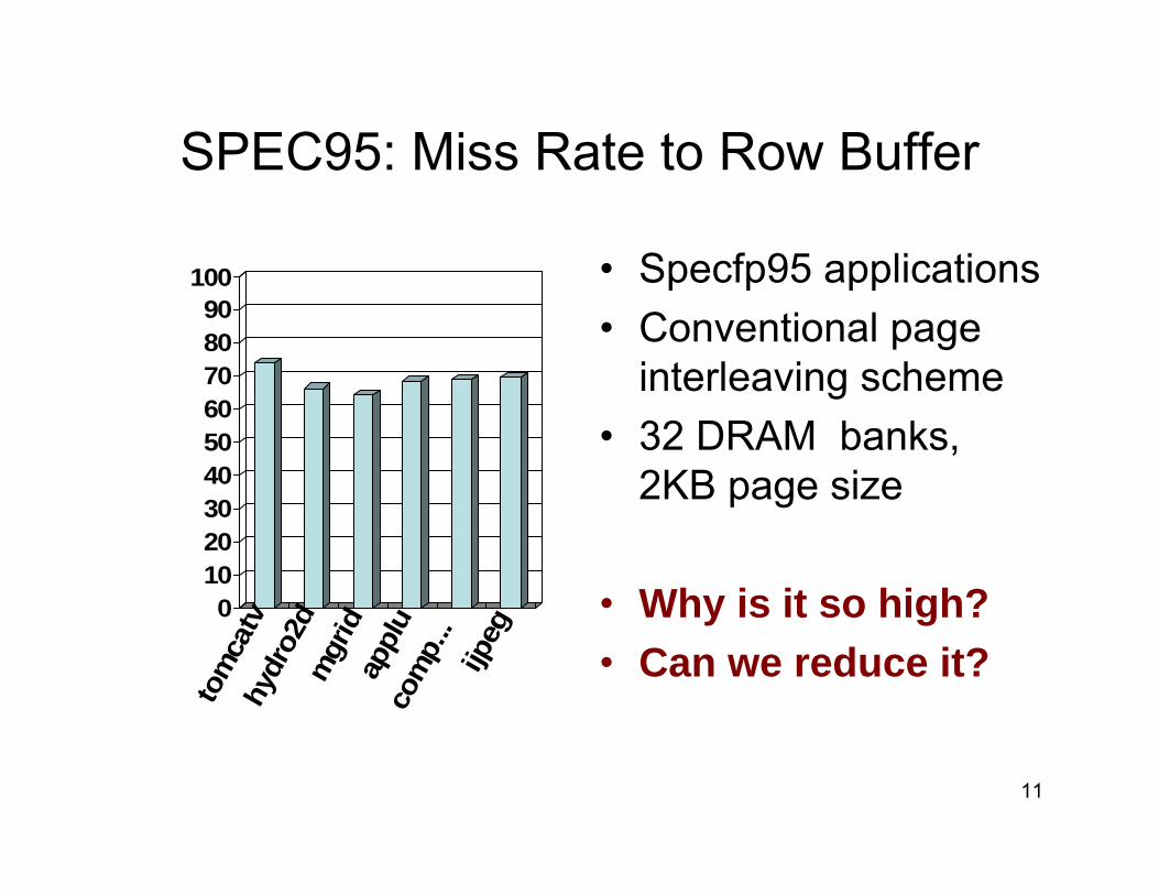
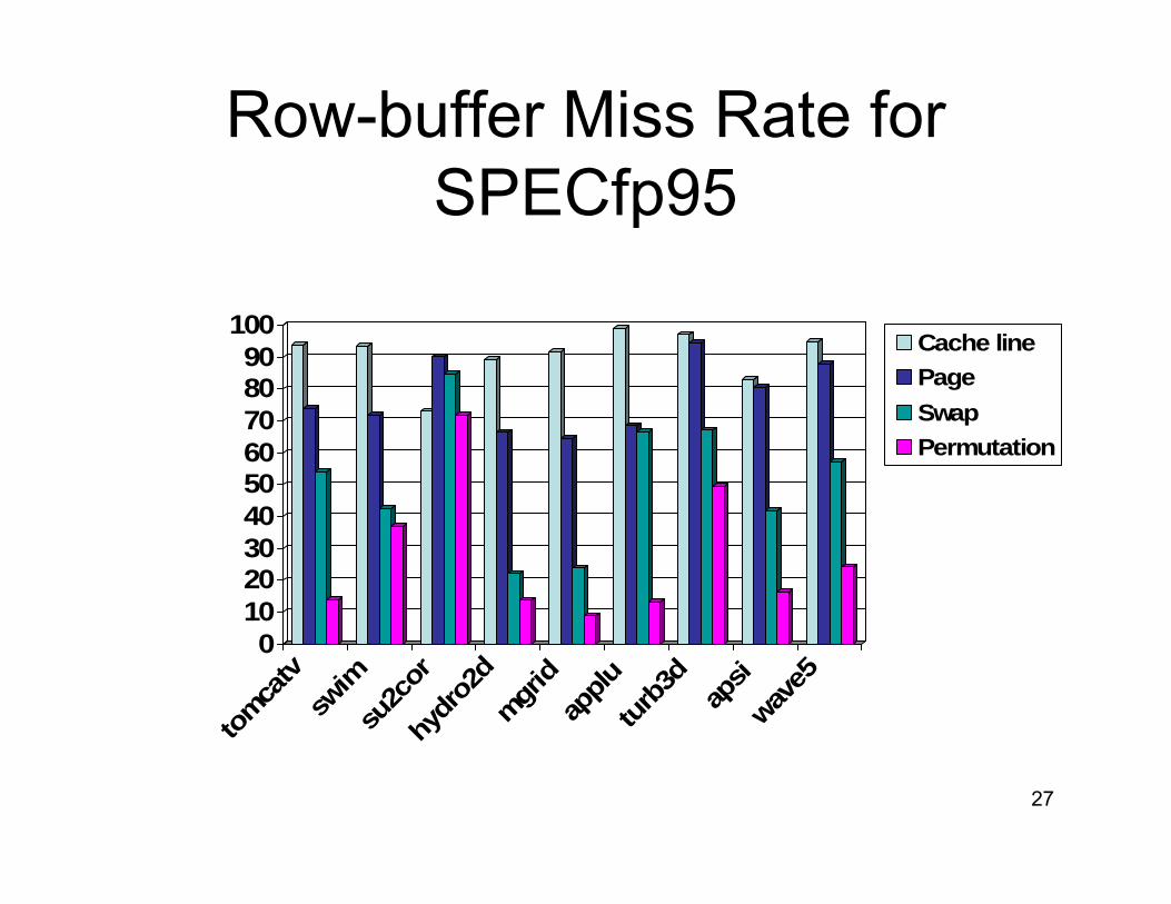
SPEC95: Miss Rate to Row Buffer
• Specfp95 applications• Conventional page
interleaving scheme• 32 DRAM banks,
2KB page size
• Why is it so high?• Can we reduce it?
0102030405060708090
100
tom
catv
hydr
o2d
mgr
idap
plu
com
p...
ijpeg

12
Effective DRAM Bandwidth
• Case 2: Row buffer misses to different banks
row access col. accessAccess 2Access 1
• Case 1: Row buffer hits
Access 2Access 1
row access col. access
col. accesscol. accesstrans. data
trans. data
trans. datatrans. data
• Case 3: Row buffer conflicts
row access col. accesscol. accessprecharge row access
bubble
trans. datatrans. dataAccess 1
Access 2

13
Parameters in a Memory System
14
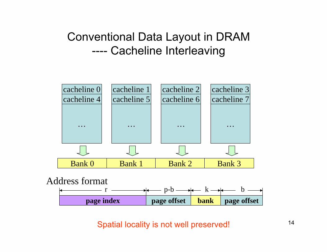
Conventional Data Layout in DRAM ---- Cacheline Interleaving
Bank 0 Bank 1 Bank 2 Bank 3
Address format
page index page offset page offsetbankr p-b bk
cacheline 0cacheline 4
…
cacheline 1cacheline 5
…
cacheline 2cacheline 6
…
cacheline 3cacheline 7
…
Spatial locality is not well preserved!
15
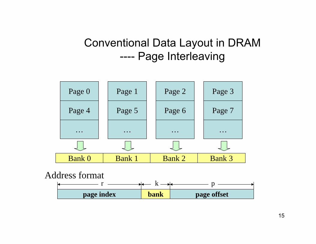
Page 0 Page 1 Page 2 Page 3
Page 4 Page 5 Page 6 Page 7
… … … …
Bank 0
Address format
Bank 1 Bank 2 Bank 3
page index page offsetbankr pk
Conventional Data Layout in DRAM ---- Page Interleaving
16
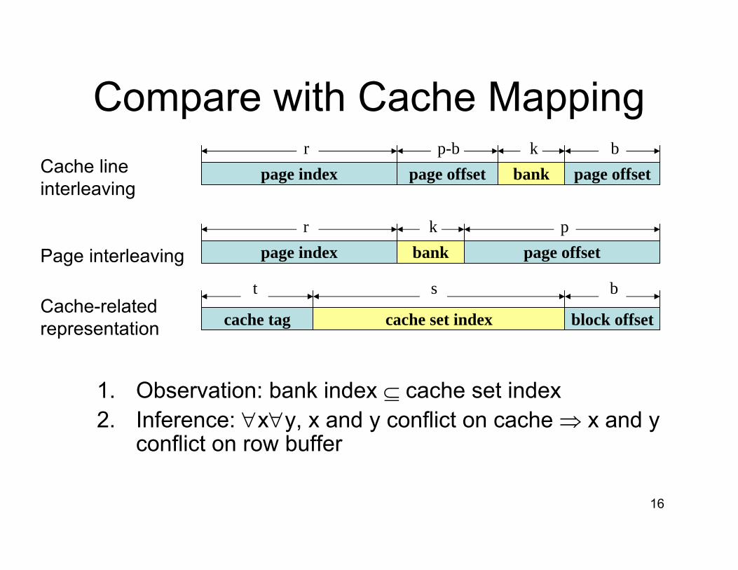
Compare with Cache Mapping
page index page offset page offset
cache tag cache set index block offset
bank
page index page offset
t s b
bank
r
r
p-b bk
pk
1. Observation: bank index ⊆ cache set index2. Inference: ∀x∀y, x and y conflict on cache ⇒ x and y
conflict on row buffer
Cache-related representation
Cache line interleaving
Page interleaving
17
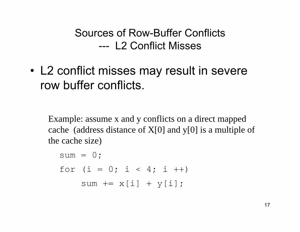
Sources of Row-Buffer Conflicts --- L2 Conflict Misses
• L2 conflict misses may result in severe row buffer conflicts.
Example: assume x and y conflicts on a direct mapped cache (address distance of X[0] and y[0] is a multiple of the cache size) sum = 0;
for (i = 0; i < 4; i ++)
sum += x[i] + y[i];
18
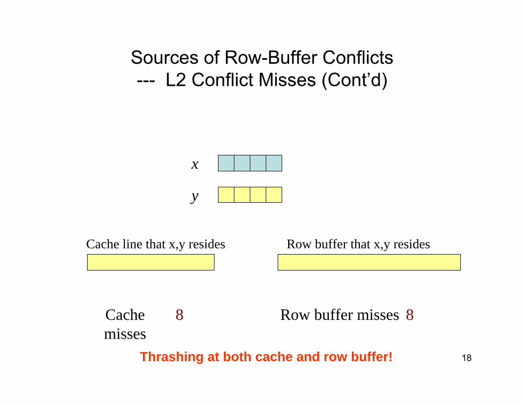
x
y
Cache misses
12345678 Row buffer misses 12345678
Cache line that x,y resides Row buffer that x,y resides
Thrashing at both cache and row buffer!
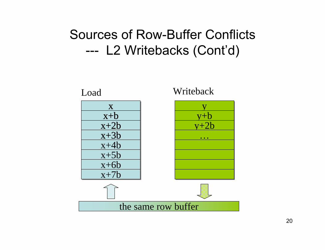
Sources of Row-Buffer Conflicts --- L2 Conflict Misses (Cont’d)
19
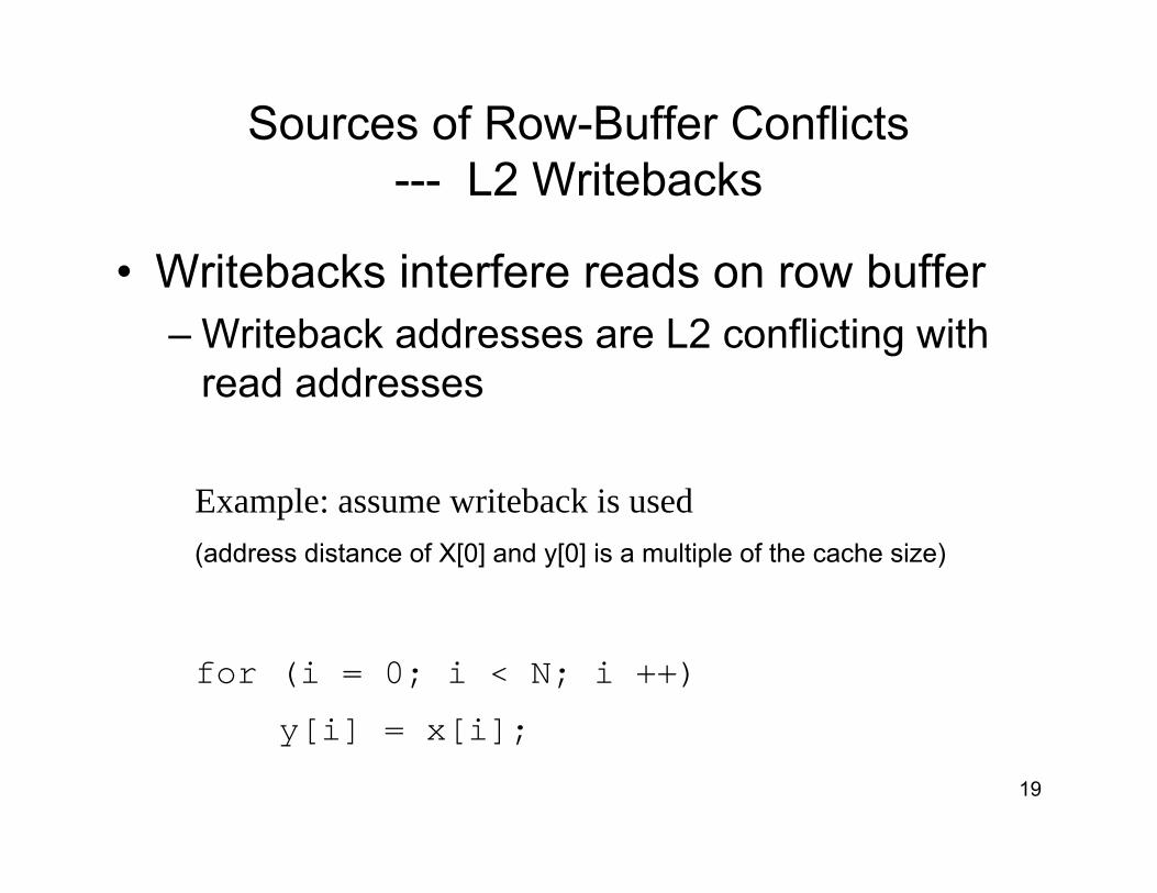
• Writebacks interfere reads on row buffer– Writeback addresses are L2 conflicting with
read addresses
Example: assume writeback is used(address distance of X[0] and y[0] is a multiple of the cache size)
for (i = 0; i < N; i ++)
y[i] = x[i];
Sources of Row-Buffer Conflicts --- L2 Writebacks
20
xxLoad
yyWriteback
x+bx+b y+by+bx+2bx+2b y+2by+2bx+3bx+3b ……
xx+bx+2bx+3bx+4bx+5bx+6bx+7b
the same row buffer
Sources of Row-Buffer Conflicts --- L2 Writebacks (Cont’d)
21
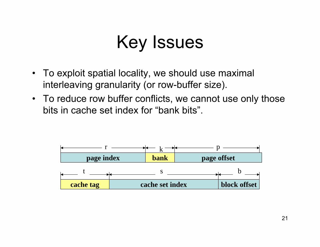
Key Issues• To exploit spatial locality, we should use maximal
interleaving granularity (or row-buffer size).• To reduce row buffer conflicts, we cannot use only those
bits in cache set index for “bank bits”.
page index page offsetbankr pk
cache tag cache set index block offset
t s b
22
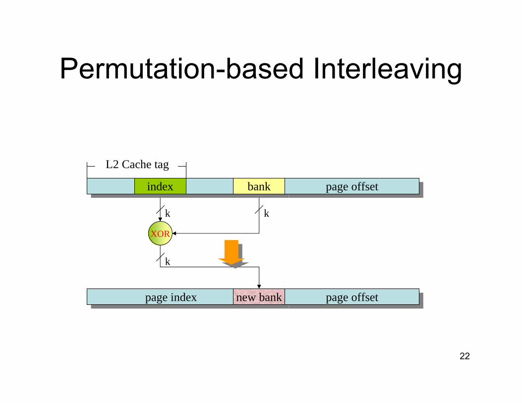
Permutation-based Interleaving
k
XOR
k
page index page index page offsetpage offsetnew bank
k
page offsetpage offsetindex bank
L2 Cache tag

23
Scheme Properties (1)• L2-conflicting addresses are distributed onto
different banks
memory banks0000000100100011010001010110011110101011
Permutation-baseinterleaving
1011 1010
1010
1001
1000
1010
1010
1010
L2 Conflicting addresses
xor
Different bank indexes
Conventionalinterleaving
Same bank indexes
24
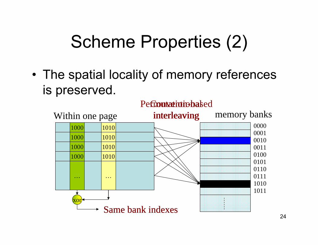
Scheme Properties (2)
• The spatial locality of memory references is preserved.
memory banks0000000100100011010001010110011110101011
1000 10101000 10101000 10101000 1010
… …
Within one pagePermutation-based
interleavingConventionalinterleaving
Same bank indexesxor
Same bank indexes
25
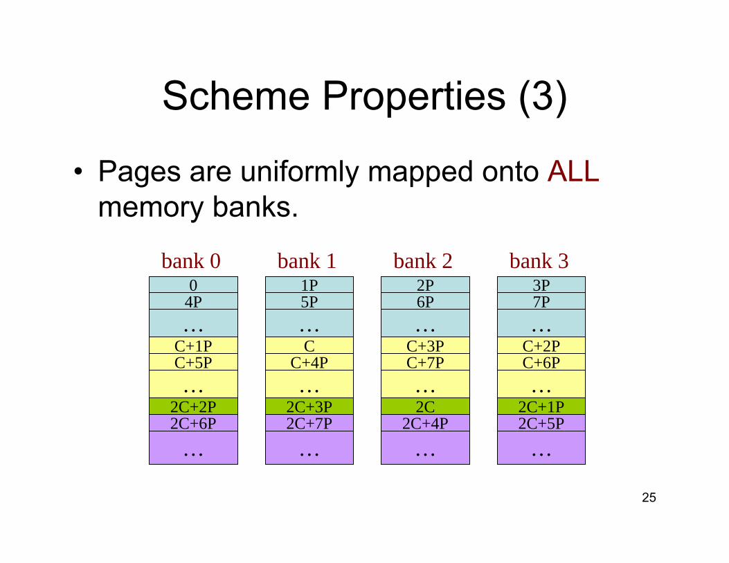
Scheme Properties (3)
• Pages are uniformly mapped onto ALLmemory banks.
C+1P
2C+2P
bank 0 bank 1 bank 2 bank 3
C
2C+3P
C+3P
2C
0 1P 2P 3P
C+2P
2C+1P
4P 5P 6P 7P… … … …
C+5P C+4P C+7P C+6P… … … …
2C+6P 2C+7P 2C+4P 2C+5P… … … …
26
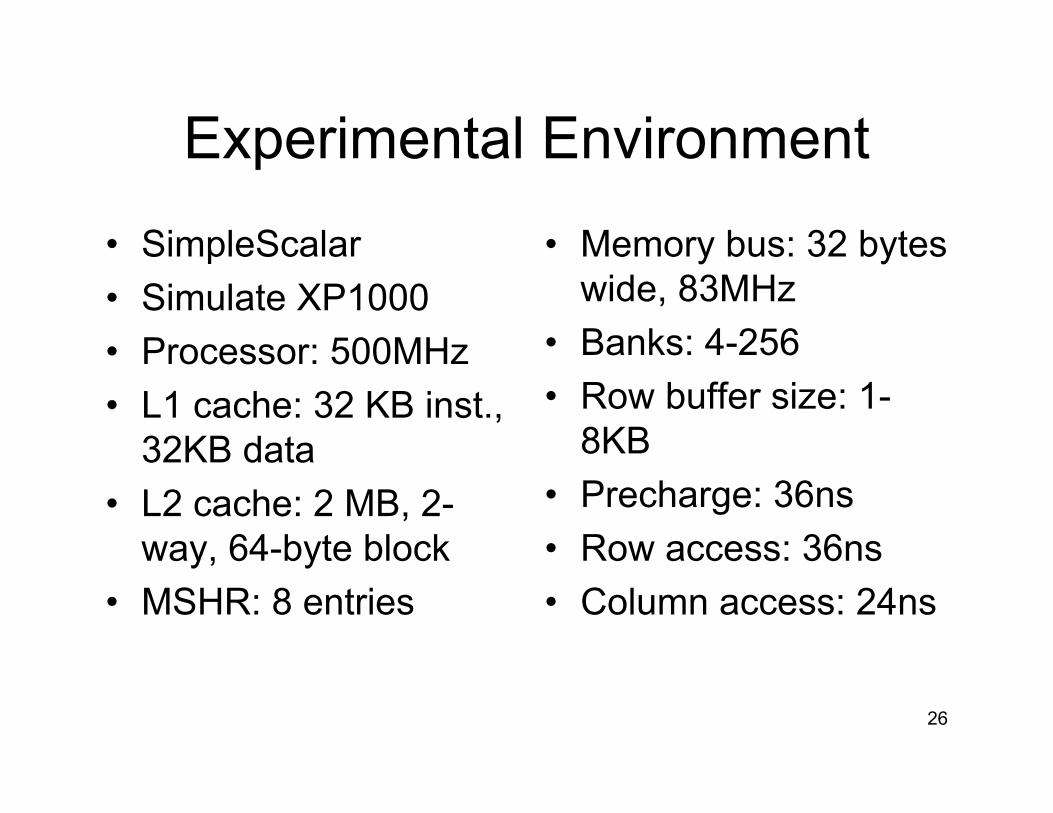
Experimental Environment
• SimpleScalar• Simulate XP1000• Processor: 500MHz• L1 cache: 32 KB inst.,
32KB data• L2 cache: 2 MB, 2-
way, 64-byte block• MSHR: 8 entries
• Memory bus: 32 bytes wide, 83MHz
• Banks: 4-256• Row buffer size: 1-
8KB• Precharge: 36ns• Row access: 36ns• Column access: 24ns
27
Row-buffer Miss Rate for SPECfp95
0102030405060708090
100
tomca
tvsw
imsu
2cor
hydr
o2d
mgrid
applu
turb3
dap
siwav
e5Cache linePageSwapPermutation
28
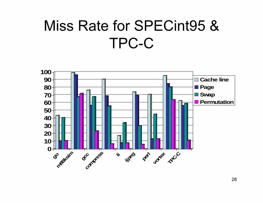
Miss Rate for SPECint95 & TPC-C
0102030405060708090
100
gom88
ksim gcc
compr
ess li
ijpeg perl
vorte
xTP
C-CCache linePageSwapPermutation
29
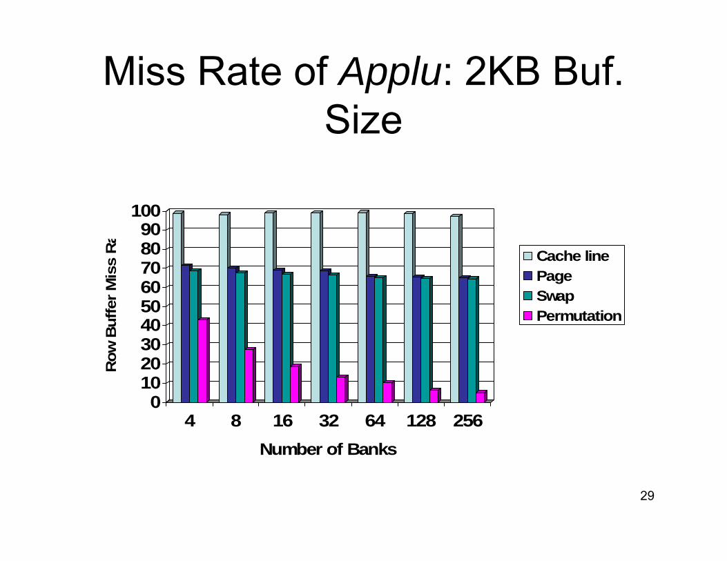
Miss Rate of Applu: 2KB Buf. Size
0102030405060708090
100
Row
Buf
fer M
iss
Ra
4 8 16 32 64 128 256Number of Banks
Cache linePageSwapPermutation
30
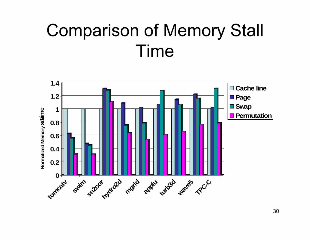
Comparison of Memory Stall Time
0
0.2
0.4
0.6
0.8
1
1.2
1.4
Nor
mal
ized
Mem
ory
Stal
l Ti
me
tomca
tvsw
imsu
2cor
hydr
o2d
mgrid
applu
turb3
dwav
e5TP
C-CCache linePageSwapPermutation
31
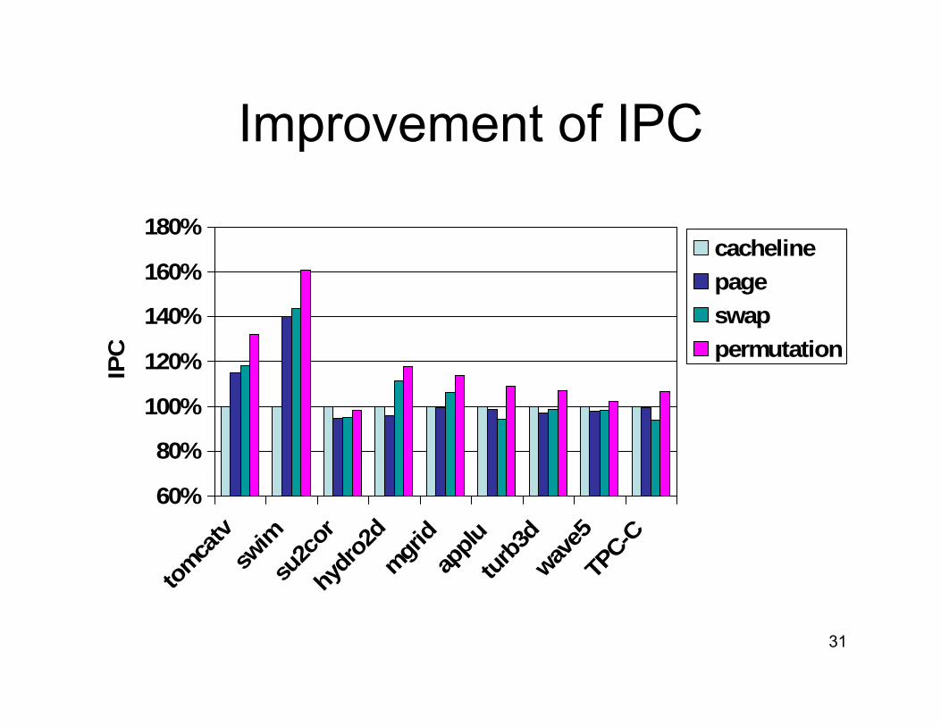
Improvement of IPC
60%
80%
100%
120%
140%
160%
180%
tomca
tvsw
imsu
2cor
hydro
2dmgri
dap
plutur
b3d
wave5
TPC-C
IPC
cachelinepageswappermutation
32
Contributions of the Work• We study interleaving for DRAM
– DRAM has a row buffer as a natural cache• We study page interleaving in the context of Superscalar
processor– Memory stall time is sensitive to both latency and
effective bandwidth – Cache miss pattern has direct impact on row buffer
conflicts and thus the access latency– Address mapping conflicts at the cache level,
including address conflicts and write-back conflicts, may inevitably propagate to DRAM memory under a standard memory interleaving method, causing significant memory access delays.
• Proposed permutation interleaving technique as a low-cost solution to these conflict problems.
33
Conclusions
• Row buffer conflicts can significantly increase memory stall time.
• We have analyzed the source of conflicts.
• Our permutation-based page interleaving scheme can effectively reduce row buffer conflicts and exploit data locality.