Embed Size (px)
Citation preview

IH2655 Design and Characterisation of Nano- and Microdevices
B. Gunnar Malm KTH
• Measurement set-up, test-structures (samples/devices)
• Types of electrical measurements • Real examples • About the lab (sign-up, preparations) • Summary
Outline

IH2655 Design and Characterisation of Nano- and Microdevices
B. Gunnar Malm KTH
• Most of the Chapters in Plummer have a subsection called:
• Mesurement Methods • Electrical measurements
• 3.4.1.2 Sheet resistance on page 113 • 6.4.3 The MOS Capacitor on page 301 • 7.4.3-4 Sheet resistance & Capacitance-
Voltage on page 398 • 11.4.2 Contact resistance/transfer
length/oxide breakdown/accel. testing p.726
Outline continued
IH2655 Design and Characterisation of Nano- and Microdevices
B. Gunnar Malm KTH
What do we want to measure? 1. Monitoring of process stability Ultra-thin gate oxides, high-k dielectrics,
sheet&contact resistance of doping and metal (silicides)
2. Performance of devices (MOSFETs) and circuits
3. Extract model parameters such as threshold voltage (VT) or whole set of SPICE parameters
• This lecture mainly covers point 1

IH2655 Design and Characterisation of Nano- and Microdevices
B. Gunnar Malm KTH
Test structures All measurements are typically on a 200-300 mm inch
wafer. Map statistics at selected locations. MOS capacitances (or split-CV) for oxide studies Different types of 4-terminal resistance structures
Van der Pauw for sheet resistance of metals, silicides, implanted/activated dopants
Cross Bridge Kelvin for contact resistance (metal-to-semiconductor)
Different MOSFET transistor sizes, use that Idrain ∝ W/L Arrays of structures for in-line probe-card measurement
(PCM)

IH2655 Design and Characterisation of Nano- and Microdevices
B. Gunnar Malm KTH
Measurement setup • Automatic 200 mm wafer prober and manual 150
mm wafers • Needle probes with micromanipulators • Measurement equipment
• 2 parameter analyzers (Keithley) with SMUs, pulse generator and coax-triax cables in Kelvin configuration)
• CV impedance bridge (Agilent/Keithley) <10 MHz
• Optical or IR-emission microscope and digital cameras

IH2655 Design and Characterisation of Nano- and Microdevices
B. Gunnar Malm KTH
Measurement setup
•Many different instruments, focus on ’semiconductor parameter analyzer’ and wafer mapping approach for IV type of measurements

IH2655 Design and Characterisation of Nano- and Microdevices
B. Gunnar Malm KTH
Test-structure layout
S
B
G
D
Transistors with different gate areas (W/L) contacted with 4 connection source, drain, gate, bulk/ground Typical probing area 80x80 µm, pitch µm 100 Probe card and switching matrix used to connect multiple devices Acronyms: DUT (device under test), PCM (probe card measurement)
IH2655 Design and Characterisation of Nano- and Microdevices
B. Gunnar Malm KTH
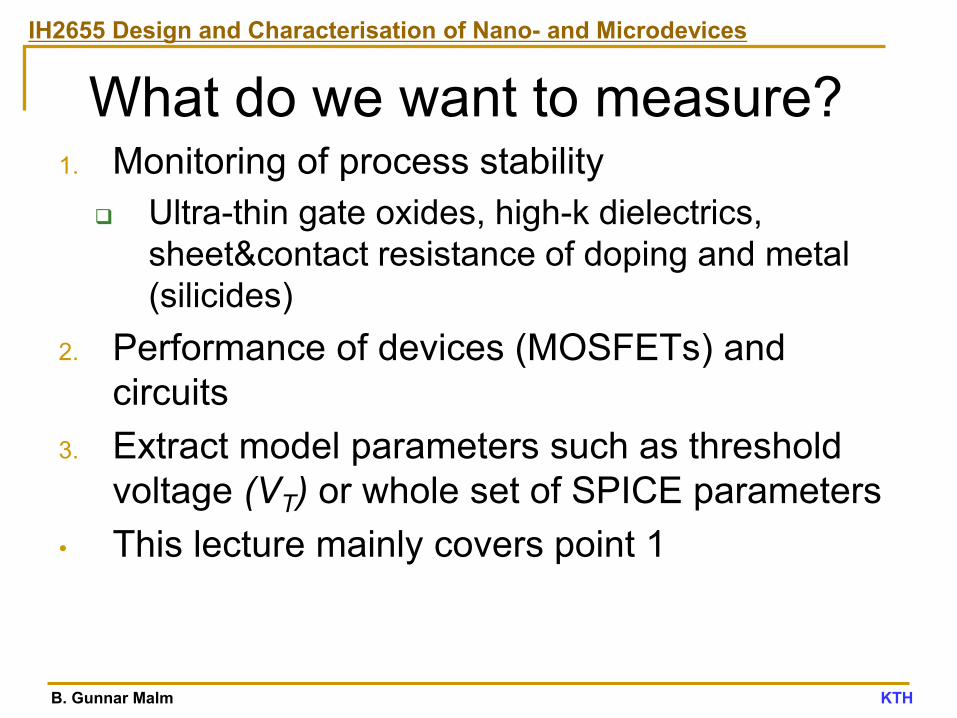
Characterization types
• IV/DC with source/measure units (SMUs), possibly preamplifiers below 1pA • High current (example small resistance of
metal/silicide line or contact) • Low current (gate and junction leakage, charge
pumping) • Pulsed to get information about defects and avoid
self-heating • AC: Impedance and C-V mainly for MOS gate
oxide but also channel mobility

IH2655 Design and Characterisation of Nano- and Microdevices
B. Gunnar Malm KTH
The 4-point principle (Kelvin)
Separate voltage and current

IH2655 Design and Characterisation of Nano- and Microdevices
B. Gunnar Malm KTH
Test-structure layout for resistance
Cross-bridge Kelvin Contact resistance, metal to highly doped silicon or Metal to silicide

IH2655 Design and Characterisation of Nano- and Microdevices
B. Gunnar Malm KTH
Test-structure layout for resistance
Cross-bridge Kelvin

IH2655 Design and Characterisation of Nano- and Microdevices
B. Gunnar Malm KTH
Test-structure layout for resistance
Van der Pauw: 2 current terminals + 2 voltage sense terminals, different length of resistor lines Metal or metal silicide lines, approx 10 – 1000 Ω
IH2655 Design and Characterisation of Nano- and Microdevices
B. Gunnar Malm KTH
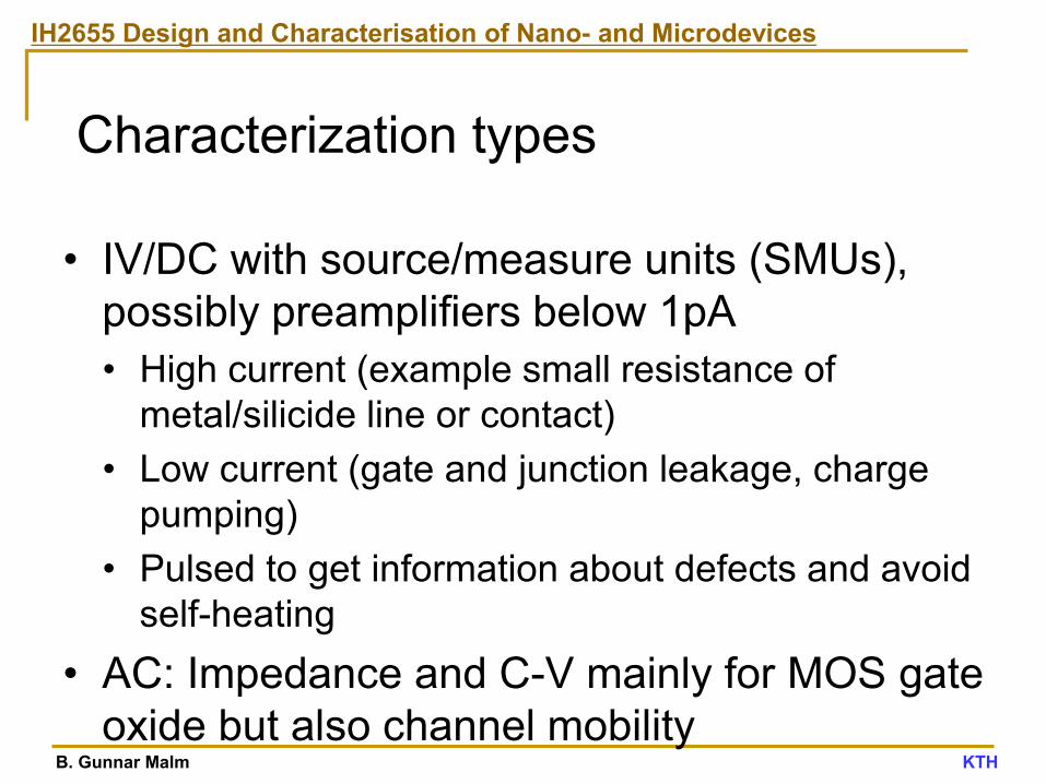
High current measurements
•Problem- resistance of cables and ’probe contacts’ will be added to the actual device •High current needed to get enough voltage drop over small resistor mΩ - 10 Ω range

IH2655 Design and Characterisation of Nano- and Microdevices
B. Gunnar Malm KTH
High current measurements
•Solution - use Kelvin connections for measurements below 100 Ω •The sense current is as small as possible (pA) •Special test-structure layout to do this on wafer

IH2655 Design and Characterisation of Nano- and Microdevices
B. Gunnar Malm KTH
Low current measurements
•Below 10 fA is possible with triax cables •Voltage resolution of 1 µV •Problems – leakage current in cables and outside interference (RF/noise)
-0.5 0.0 0.5 1.0 1.5 2.0 2.510-15
1x10-13
1x10-11
1x10⁻⁹
1x10⁻⁷
1x10⁻⁵
1x10⁻³
1f
100f
10p
1n
100n
10µ
1m
Drain
, gate
curre
nt (A
)
Gate voltage (V)
ID IG
LG x WG = 45 nm x 10 µm
IH2655 Design and Characterisation of Nano- and Microdevices
B. Gunnar Malm KTH
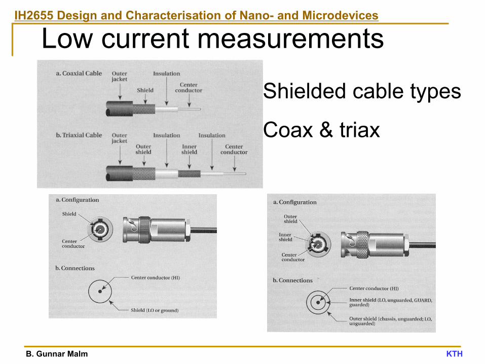
Low current measurements
Shielded cable types
Coax & triax

IH2655 Design and Characterisation of Nano- and Microdevices
B. Gunnar Malm KTH
Low current measurements
Shielded cables reduce noise and interference Noise current is shunted to ground Voltage difference between signal conductor and grounded shield causes resistive leakage

IH2655 Design and Characterisation of Nano- and Microdevices
B. Gunnar Malm KTH
Low current measurements
Resistive leakage to shield around 1 nA, depends on applied voltage

IH2655 Design and Characterisation of Nano- and Microdevices
B. Gunnar Malm KTH
Low current measurements
Use guard for measurements below 1 nA, solves problem of potential difference and resistive leakage Voltage buffer (x1 amplifier) sets the potential on the guard Leakage current flows between guard and ground potential
IH2655 Design and Characterisation of Nano- and Microdevices
B. Gunnar Malm KTH
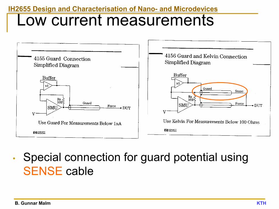
Low current measurements
• Special connection for guard potential using SENSE cable

IH2655 Design and Characterisation of Nano- and Microdevices
B. Gunnar Malm KTH
Low current measurements
•The probe needle is also shielded, small radius 5 µm

IH2655 Design and Characterisation of Nano- and Microdevices
B. Gunnar Malm KTH 23
L4: Electrical Characterization - Concept Test 4.1 4.1 Electrical characterization is an important step in
the wafer fabrication flow: Which statements are true?
(One or more answers may be correct)
A. Measurements are usually done on completed wafers
B. Measurements are usually done during the process flow
C. Measurements are usually done on special test structures
D. Measurements are usually done on transistors
E. None of the above.

IH2655 Design and Characterisation of Nano- and Microdevices
B. Gunnar Malm KTH
Background – MOS gate oxide
New high-k material introduced to reduce gate leakage Thicker layer – lower leakage Bulk & interface decfects, long term stability, stress effects et.c. must be characterized
IH2655 Design and Characterisation of Nano- and Microdevices
B. Gunnar Malm KTH
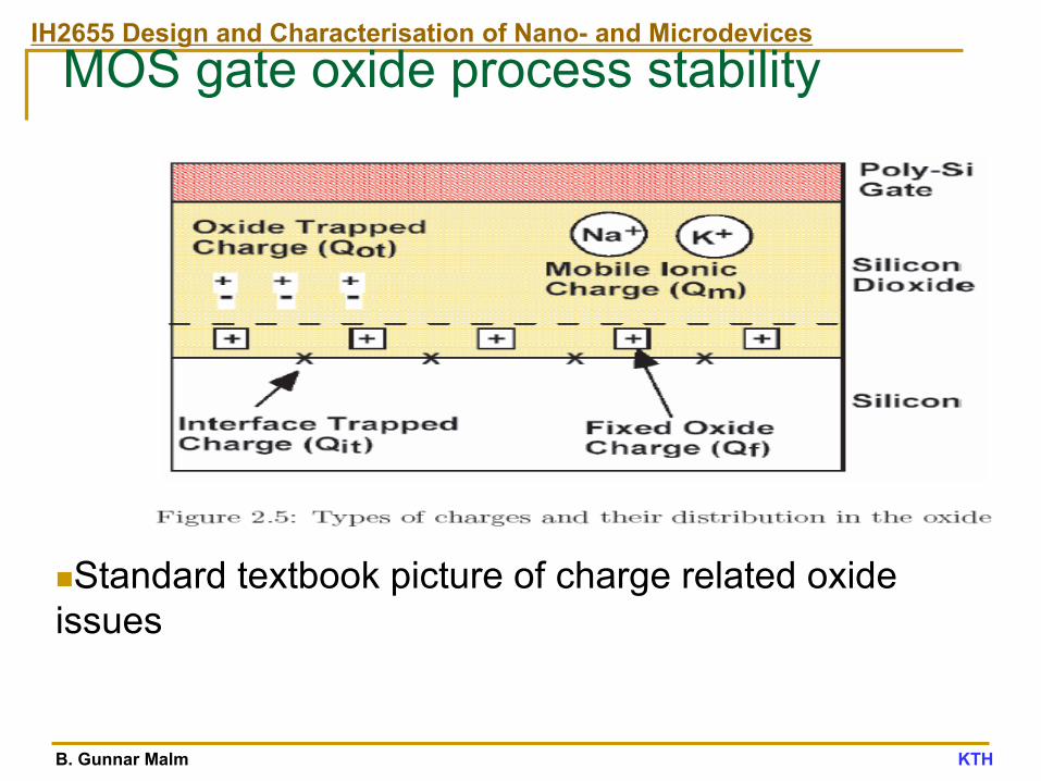
MOS gate oxide process stability
Standard textbook picture of charge related oxide issues

IH2655 Design and Characterisation of Nano- and Microdevices
B. Gunnar Malm KTH
MOS gate oxide process stability
Gate oxide thickness and quality CV - thickness, trapped charge (also
VT-shift) CP - interface states IV - oxide integrity, leakage current,
breakdown field, charge-to-breakdown (QDB, TDDB) , hot-carrier injection (HCI), stress (NBTI)
IH2655 Design and Characterisation of Nano- and Microdevices
B. Gunnar Malm KTH
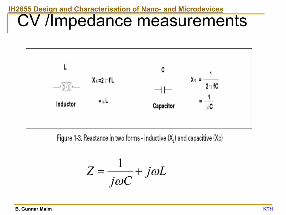
CV /Impedance measurements
LjCj
Z ωω
+=1
IH2655 Design and Characterisation of Nano- and Microdevices
B. Gunnar Malm KTH
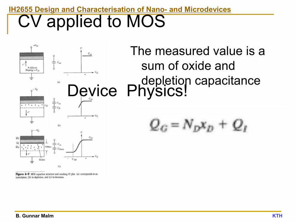
CV applied to MOS The measured value is a
sum of oxide and depletion capacitance
Device Physics!

IH2655 Design and Characterisation of Nano- and Microdevices
B. Gunnar Malm KTH
CV applied to MOS
CV technique could be used to study defects, we focus on charge pumping later
IH2655 Design and Characterisation of Nano- and Microdevices
B. Gunnar Malm KTH
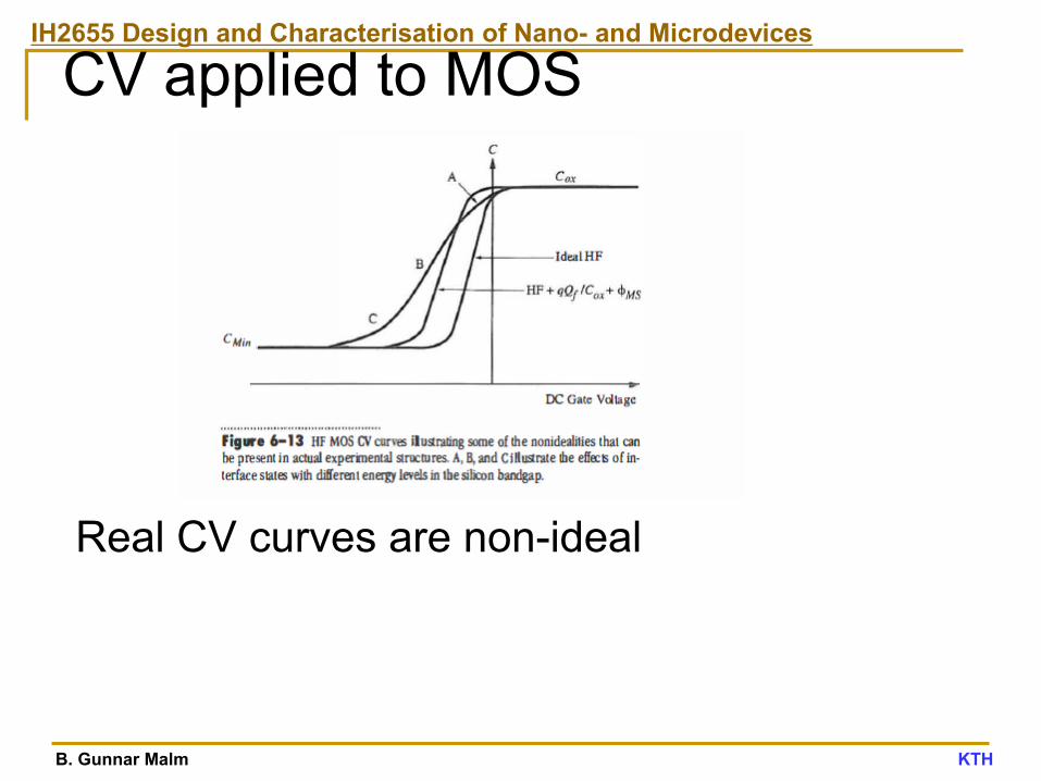
CV applied to MOS
Real CV curves are non-ideal

IH2655 Design and Characterisation of Nano- and Microdevices
B. Gunnar Malm KTH
MOS gate oxide process stability
C [pF]:2.86±0.43 Q-value:12.53±8.37
Vfb [V]:-0.16±0.12 delta Vfb [mV] :41.00±26.15
Gate oxide thickness and quality - 100 mm wafer map, metal-gate + high-k
Influence of (trapped) charges
Hysteresis due to ’interface’ states
Capacitance ∝ 1/ oxide thickness
Q-value measure of capacitance/resistance

IH2655 Design and Characterisation of Nano- and Microdevices
B. Gunnar Malm KTH
MOS gate oxide process stability
Basic IV measurements of leakage current in thin gate oxides
IH2655 Design and Characterisation of Nano- and Microdevices
B. Gunnar Malm KTH
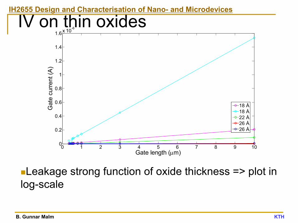
IV on thin oxides
Leakage strong function of oxide thickness => plot in log-scale
0 1 2 3 4 5 6 7 8 9 100
0.2
0.4
0.6
0.8
1
1.2
1.4
1.6x 10⁻⁶
Gate length (µm)
Gat
e cu
rrent
(A)
18 Å18 Å22 Å26 Å26 Å

IH2655 Design and Characterisation of Nano- and Microdevices
B. Gunnar Malm KTH
IV on thin oxides
Leakage increased by 5 orders of magnitude by scaling oxide less than 50 %! Variation for nominally identical devices caused by?
0 1 2 3 4 5 6 7 8 9 1010-14
10-12
10-10
10-8
10-6
10-4
Gate length (µm)
Gat
e cu
rrent
(A)
18 Å18 Å22 Å26 Å26 Å
Actually 50 nm gate length devices

IH2655 Design and Characterisation of Nano- and Microdevices
B. Gunnar Malm KTH
MOS gate oxide process stability
Split CV on MOSFETs, source & drain reverse biased Use the actual device as a test-structure, measure the capacitance of the active carriers (electrons) in the channel inversion layer MOS capacitance probes the accumulated surface, using (holes)

IH2655 Design and Characterisation of Nano- and Microdevices
B. Gunnar Malm KTH
CV on thin oxides
Example of Q-value dependence on oxide thickness, frequency (100/300 kHz), and gate leakage current
0.0 0.5 1.0 1.5 2.0 2.50.0
1.0x10⁻¹²
2.0x10⁻¹²
3.0x10⁻¹²
4.0x10⁻¹²
5.0x10⁻¹²
6.0x10⁻¹²
7.0x10⁻¹²
18 Å 22 Å 26 Å
Capa
citan
ce (F
)
Gate Voltage (V)
0 2
0
100
Q-v
alue

IH2655 Design and Characterisation of Nano- and Microdevices
B. Gunnar Malm KTH
MOS gate oxide process stability
-2.5 -2 -1.5 -1 -0.5 0 0.5 10
1
2
3
4
5 x 10-12
Gate Voltage (V)
Gat
e-ch
anne
l cap
acita
nce
[F]
Sweep direction
Delta ’Vfb’ hysteresis
Shift in Vfb
Capacitance in inversion for pMOSFET
Split CV on MOSFETs, two devices on the same wafer
IH2655 Design and Characterisation of Nano- and Microdevices
B. Gunnar Malm KTH
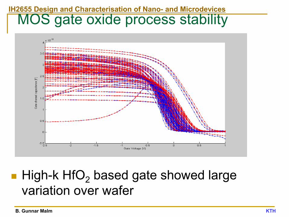
MOS gate oxide process stability
High-k HfO2 based gate showed large variation over wafer

IH2655 Design and Characterisation of Nano- and Microdevices
B. Gunnar Malm KTH 39
L4: Electrical Characterization - Concept Test 4.1 4.2 Electrical characterization is used to evaluate new
materials: Which statements are true? (One or more answers may be correct)
A. Capacitance-Voltage (CV) is the best technique to
probe defects and thickness of thin oxides
B. Current-Voltage (IV) is the best technique to probe defects and thickness of thin oxides
C. Both IV and CV are needed to probe defects in thin oxides
D. Both IV and CV are needed to probe thickness of thin oxide
E. None of the above.
IH2655 Design and Characterisation of Nano- and Microdevices
B. Gunnar Malm KTH
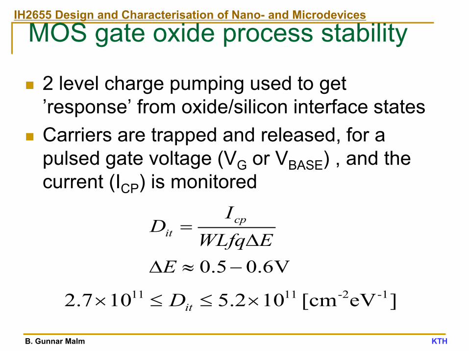
2 level charge pumping used to get ’response’ from oxide/silicon interface states
Carriers are trapped and released, for a pulsed gate voltage (VG or VBASE) , and the current (ICP) is monitored
V6.05.0 −≈∆∆
=
EEWLfq
ID cp
it
]eV[cm 102.5107.2 -1-21111 ×≤≤× itD
MOS gate oxide process stability
IH2655 Design and Characterisation of Nano- and Microdevices
B. Gunnar Malm KTH
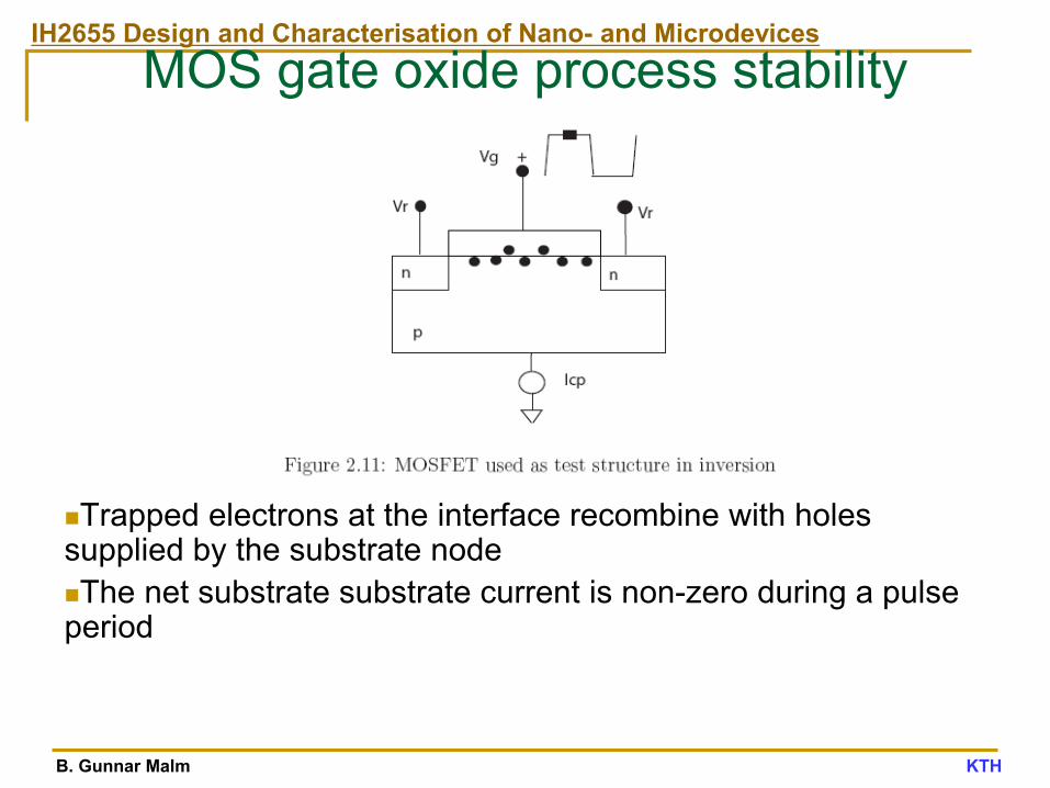
MOS gate oxide process stability
Trapped electrons at the interface recombine with holes supplied by the substrate node The net substrate substrate current is non-zero during a pulse period

IH2655 Design and Characterisation of Nano- and Microdevices
B. Gunnar Malm KTH
MOS gate oxide process stability
Sweeping base voltage VBASE or amplitude ∆Vfor the pulse Pulse generator with nanosecond rise/fall time needed

IH2655 Design and Characterisation of Nano- and Microdevices
B. Gunnar Malm KTH
MOS gate oxide process stability
Maximum ICP is a measure of DIT ICP should scale with gate length for short
transistors according to equation
IH2655 Design and Characterisation of Nano- and Microdevices
B. Gunnar Malm KTH
MOS gate oxide process stability
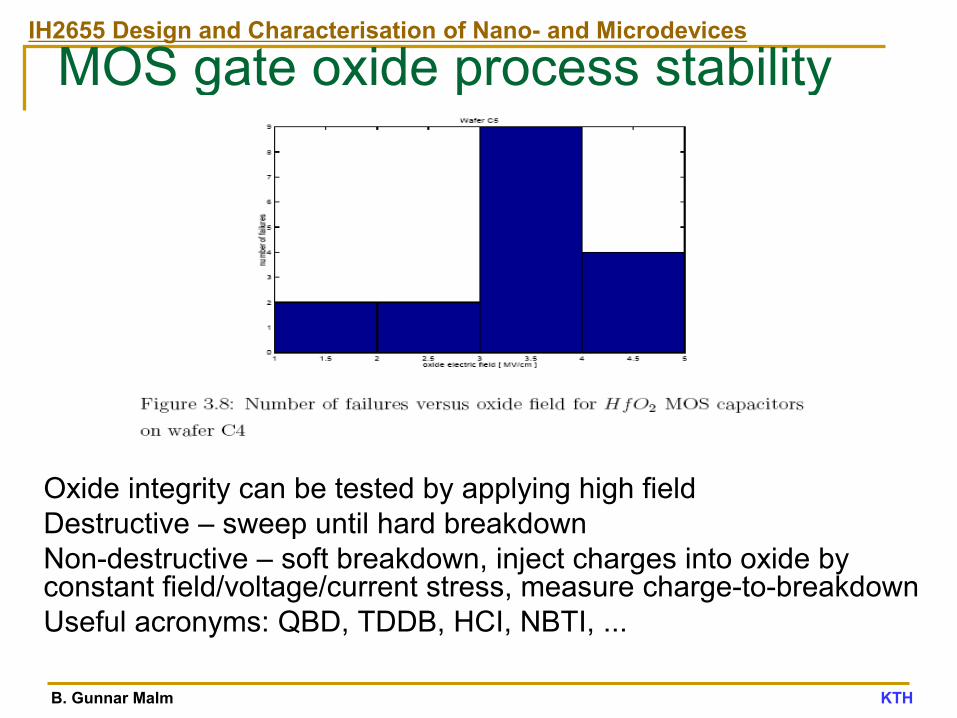
Oxide integrity can be tested by applying high field Destructive – sweep until hard breakdown Non-destructive – soft breakdown, inject charges into oxide by constant field/voltage/current stress, measure charge-to-breakdown Useful acronyms: QBD, TDDB, HCI, NBTI, ...

IH2655 Design and Characterisation of Nano- and Microdevices
B. Gunnar Malm KTH
Monitoring of process stability
Sheet-resistance measurements Uniformity of metal-silicide formation (resistance) across wafer Color shift (bluish to red) indicates problem!
IH2655 Design and Characterisation of Nano- and Microdevices
B. Gunnar Malm KTH
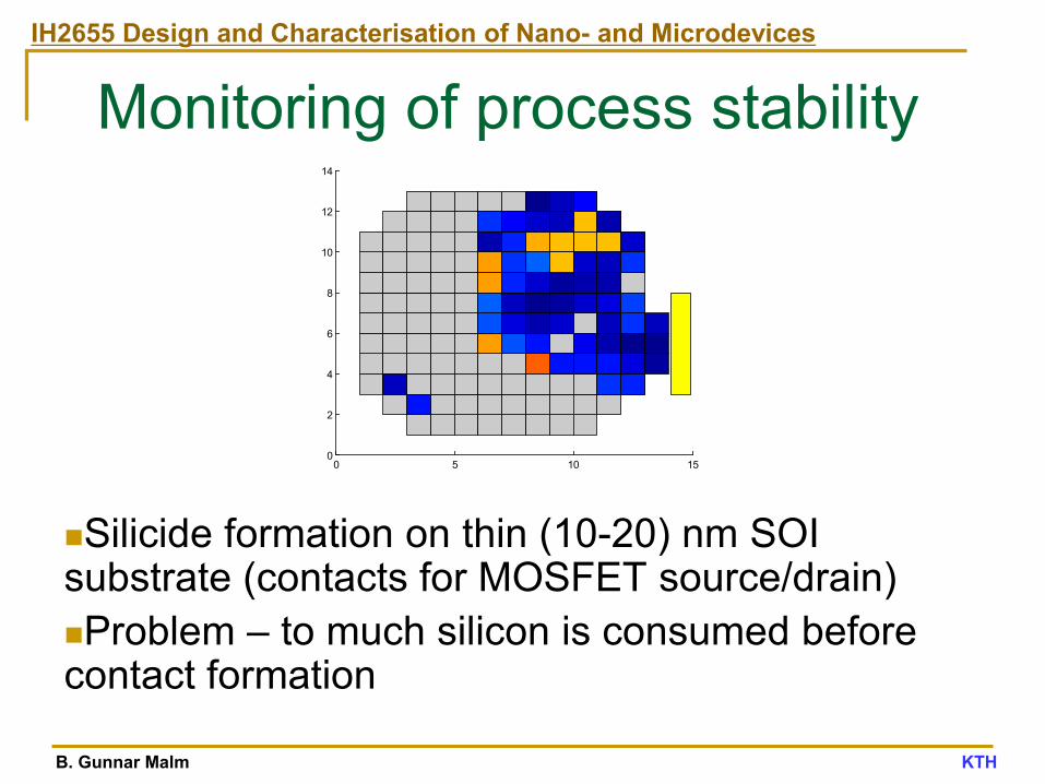
Monitoring of process stability
Silicide formation on thin (10-20) nm SOI substrate (contacts for MOSFET source/drain) Problem – to much silicon is consumed before contact formation
0 5 10 150
2
4
6
8
10
12
14

IH2655 Design and Characterisation of Nano- and Microdevices
B. Gunnar Malm KTH
Monitoring of process stability
Gate length variation - critical dimension (CD) control Monitor gate electrode in 4-point resistor configuration across wafer, plot in Weibull graph!

IH2655 Design and Characterisation of Nano- and Microdevices
B. Gunnar Malm KTH
About the lab
Sign-up sheets distributed in class Mandatory preparation 48 h in advance,
email to: [email protected] PREL Instructions for 2013 available from
today, general theme IV measurement of high-k/metal gate wafers see above, also high mobility substrates
Report due 1 week after completed lab, submit by email.

IH2655 Design and Characterisation of Nano- and Microdevices
B. Gunnar Malm KTH
Summary
Combination of IV, CV, chargepumping needed to characterize wafer mainly after completed process flow
Low-level measurements use special shielding techniques and/or calibration
Special layout of test structures for challenging measurements – sometimes the transistor is the test structure

IH2655 Design and Characterisation of Nano- and Microdevices
B. Gunnar Malm KTH
Sources • IEEE Spectrum, ”The high-k solution,” online, Oct,
2007. • Keithley – Low level measurements 6th ed • Keithley – Overcoming the Measurement Challenges
of Advance Semiconductor Technologies 1st ed • Agilent Technologies Impedance Measurement
Handbook 2003 (Online) • Schroder – Semiconductor Material and Device
Characterization • Plummer et al – Silicon VLSI Technology • Buono, Master Thesis, KTH, 2007