Embed Size (px)
Citation preview
Lecture 3Types of Solar Cells (experiment )-
3 generationsGeneration 1:
Single- and poly-Crystalline SiliconGrowth, impurity diffusion, contacts
Modules, interconnectionGeneration 2:
Polycrystalline thin films, crystal structure, deposition techniquesCdS/CdTe (II-VI) cells
CdS/Cu(In,Ga)Se2 cellsAmorphous Si:H cells
Generation 3:High-efficiency Multi-junction Concentrator Solar Cells based on III-V’s and III-V ternary analogs
Dye-sensitized cellsOrganic (excitonic) cells
Polymeric CellsNanostructured cells including Multi-carrier per photon cells, quantum dot and quantum
confined cells
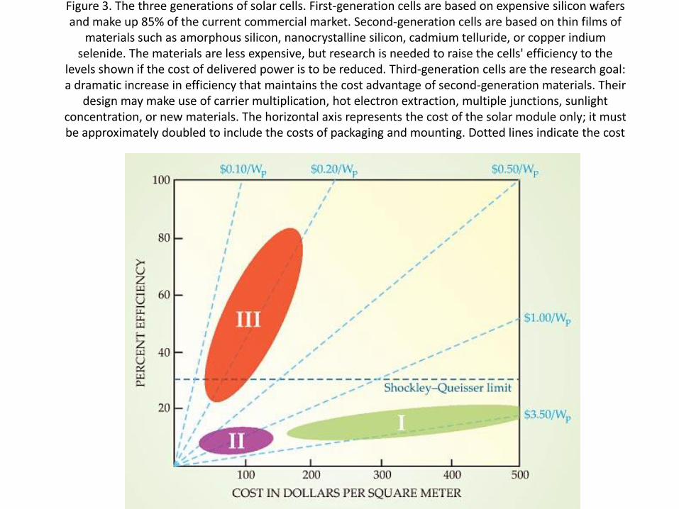
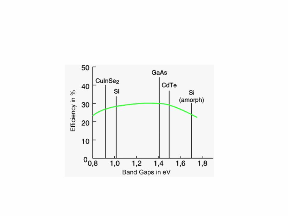
Figure 3. The three generations of solar cells. First-generation cells are based on expensive silicon wafers and make up 85% of the current commercial market. Second-generation cells are based on thin films of
materials such as amorphous silicon, nanocrystalline silicon, cadmium telluride, or copper indium selenide. The materials are less expensive, but research is needed to raise the cells' efficiency to the
levels shown if the cost of delivered power is to be reduced. Third-generation cells are the research goal: a dramatic increase in efficiency that maintains the cost advantage of second-generation materials. Their
design may make use of carrier multiplication, hot electron extraction, multiple junctions, sunlight concentration, or new materials. The horizontal axis represents the cost of the solar module only; it must be approximately doubled to include the costs of packaging and mounting. Dotted lines indicate the cost
per watt of peak power (Wp). (Adapted from ref. 2,) Green.)
Generation I.
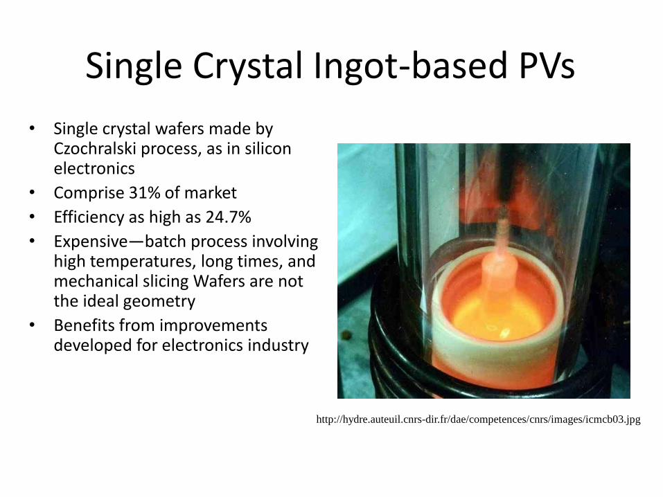
Single Crystal Ingot-based PVs
• Single crystal wafers made by Czochralski process, as in silicon electronics
• Comprise 31% of market
• Efficiency as high as 24.7%
• Expensive—batch process involving high temperatures, long times, and mechanical slicing Wafers are not the ideal geometry
• Benefits from improvements developed for electronics industry
http://hydre.auteuil.cnrs-dir.fr/dae/competences/cnrs/images/icmcb03.jpg
6.6.06 - 8.6.06Clemson Summer School
Dr. Karl Molter / FH Trier / [email protected]
5
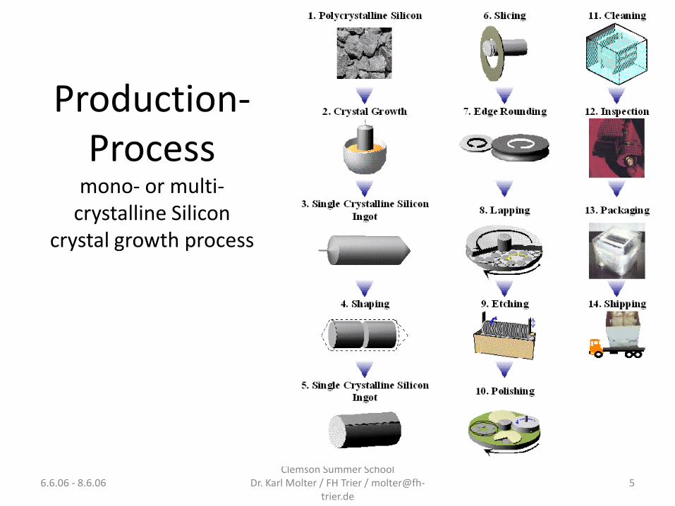
Production-Process
mono- or multi-crystalline Silicon
crystal growth process
6.6.06 - 8.6.06Clemson Summer School
Dr. Karl Molter / FH Trier / [email protected]
6
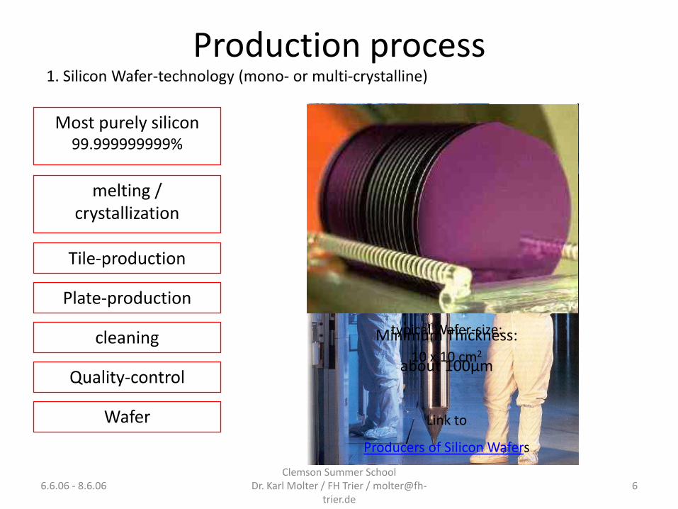
Production process1. Silicon Wafer-technology (mono- or multi-crystalline)
Tile-production
Plate-production
cleaning
Quality-control
Wafer
Most purely silicon99.999999999%
Occurence:
Siliconoxide (SiO2)
= sand
melting / crystallization
SiO2 + 2C = Si + 2CO
Mechanical cutting:
Thickness about 300µm
Minimum Thickness:
about 100µm
typical Wafer-size:
10 x 10 cm2
Link to
Producers of Silicon Wafers
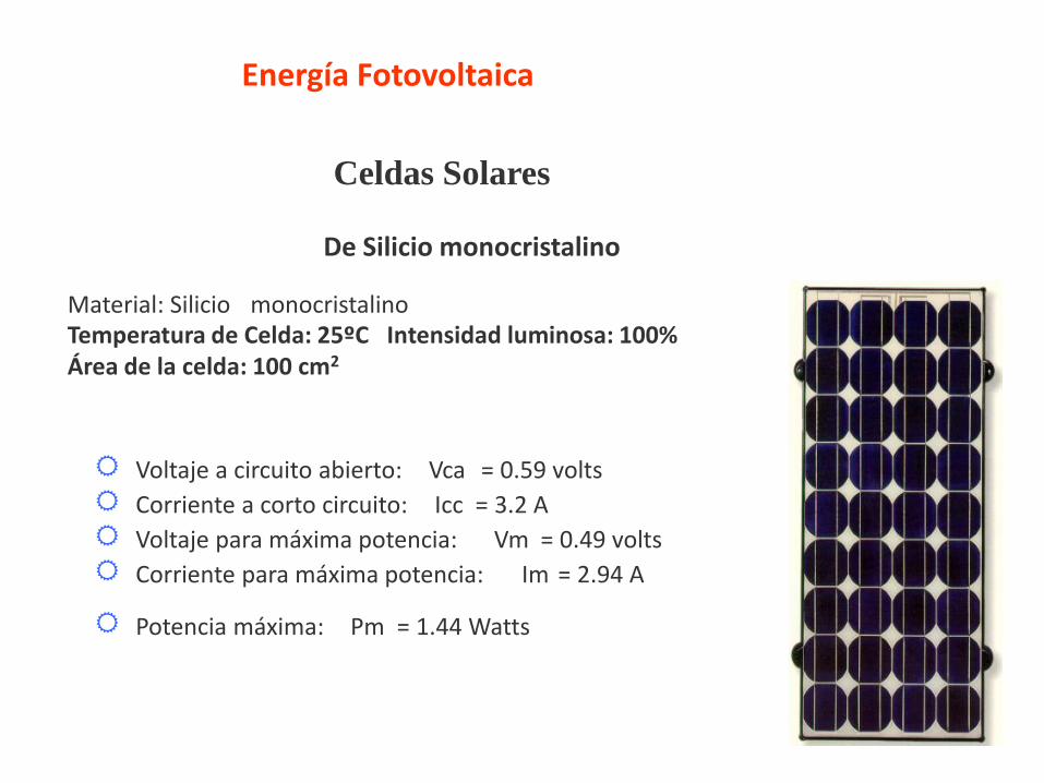
Energía Fotovoltaica
Celdas Solares
De Silicio monocristalino
Material: Silicio monocristalinoTemperatura de Celda: 25ºC Intensidad luminosa: 100%Área de la celda: 100 cm2
Voltaje a circuito abierto: Vca = 0.59 volts
Corriente a corto circuito: Icc = 3.2 A
Voltaje para máxima potencia: Vm = 0.49 volts
Corriente para máxima potencia: Im = 2.94 A
Potencia máxima: Pm = 1.44 Watts
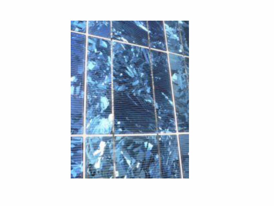
Polycrystalline Ingot-based PVs
• Fastest-growing technology involves casting Si in disposable crucibles
• Grains mm or cm scale, forming columns in solidification direction
• Efficiencies as high as 20% in research
• Production efficiencies 13-15%
• Faster, better geometry, but still requires mechanical slicing
Polycrystalline Si Ribbon PVs• String method
– Two strings drawn through melt stabilize ribbon edge– Ribbon width: 8 cm
• Carbon foil method (edge-defined film-fed growth, EFG)– Si grows on surface of a carbon foil die– Die is currently an octagonal prism, with side length 12.5
cm
• Pros and Cons– Method can be continuous– Requires no mechanical slicing– Efficiencies similar to other polycrystalline PVs– Balancing growth rate, ribbon thickness and width
Generation II.
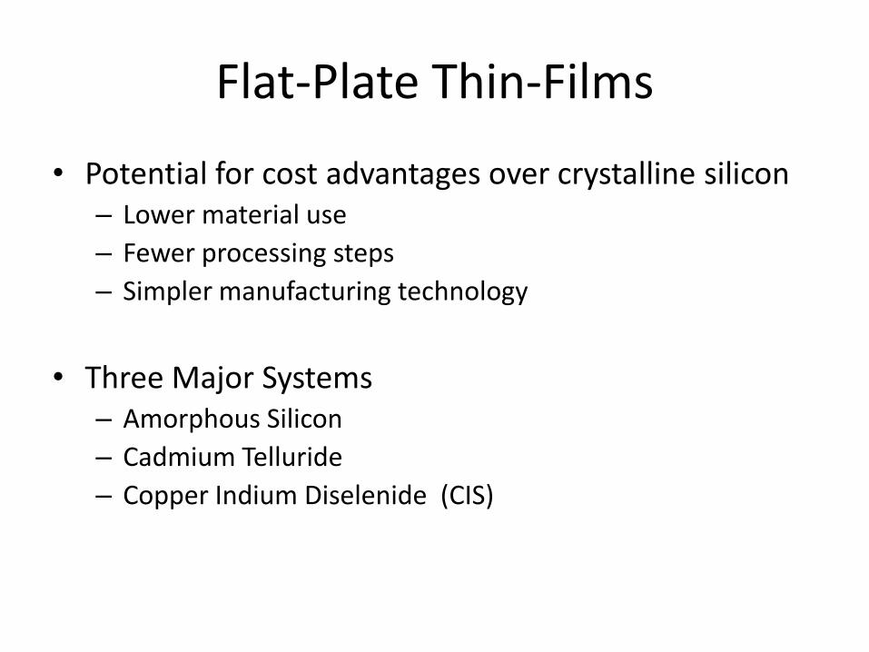
Flat-Plate Thin-Films
• Potential for cost advantages over crystalline silicon– Lower material use
– Fewer processing steps
– Simpler manufacturing technology
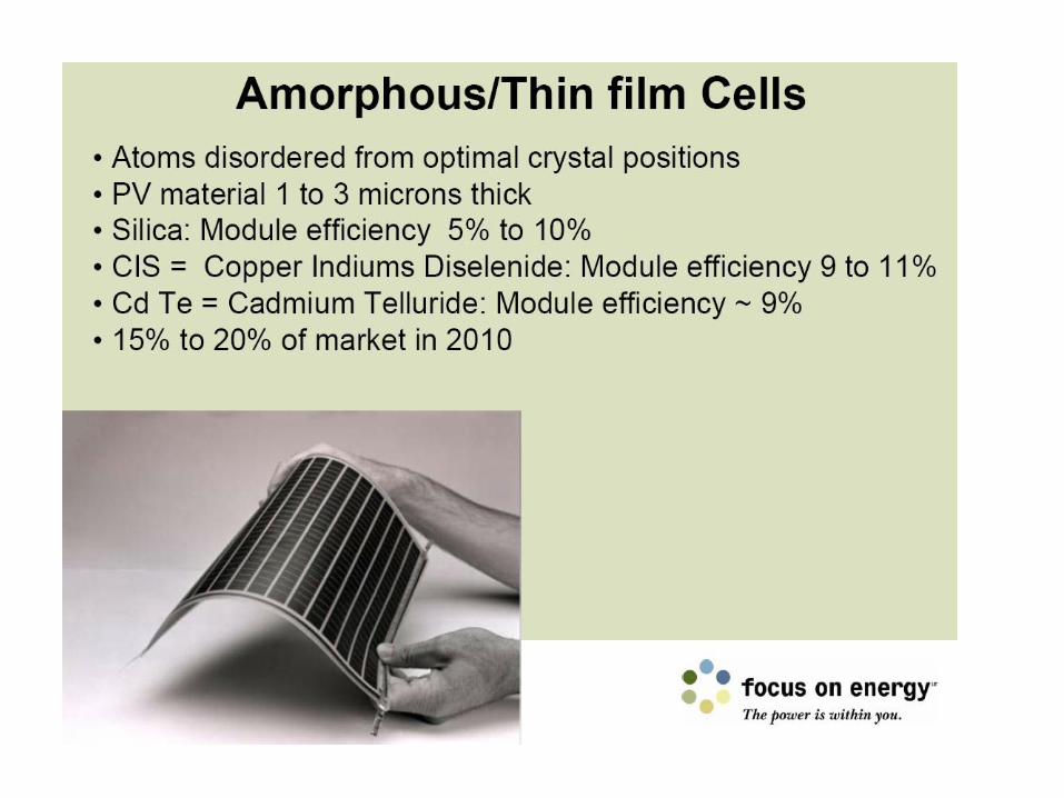
• Three Major Systems– Amorphous Silicon
– Cadmium Telluride
– Copper Indium Diselenide (CIS)
6.6.06 - 8.6.06Clemson Summer School
Dr. Karl Molter / FH Trier / [email protected]
14
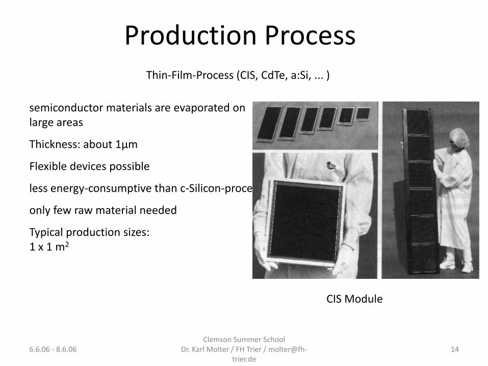
Production Process
semiconductor materials are evaporated on large areas
Thickness: about 1µm
Flexible devices possible
less energy-consumptive than c-Silicon-process
only few raw material needed
Typical production sizes:1 x 1 m2
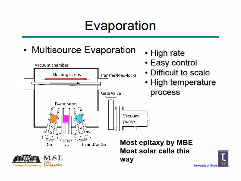
Thin-Film-Process (CIS, CdTe, a:Si, ... )
CIS Module
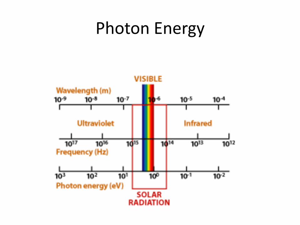
Photon Energy
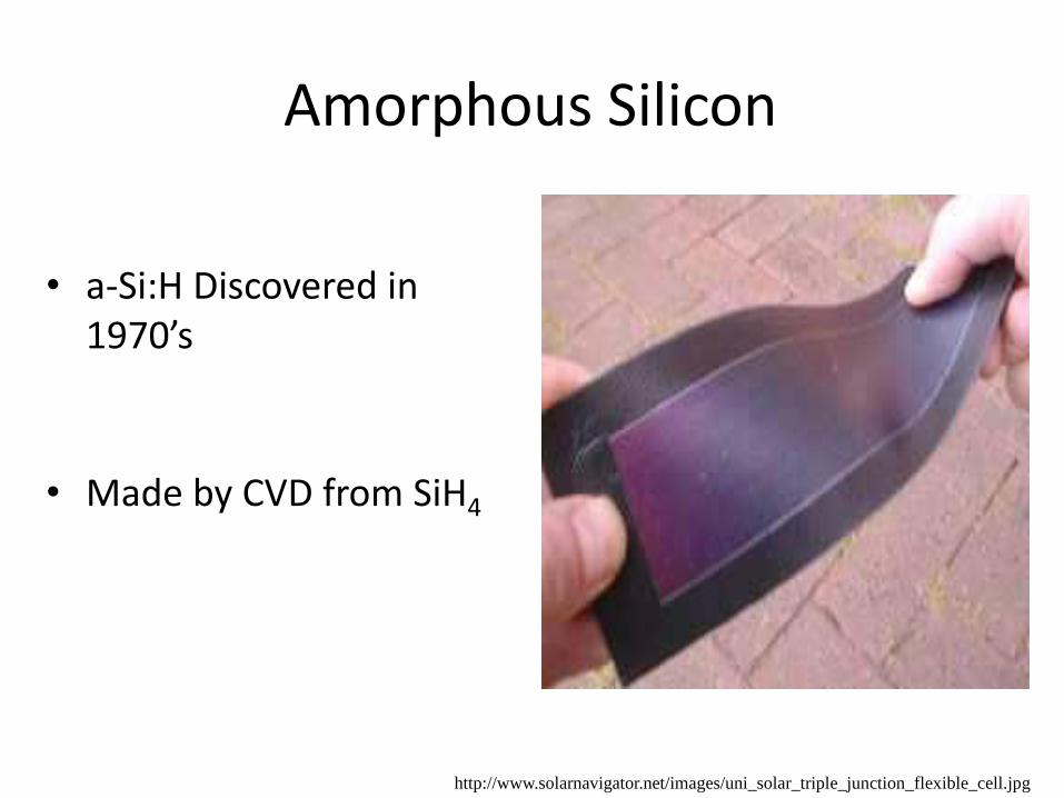
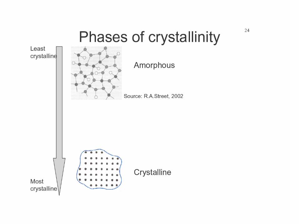
Amorphous Silicon
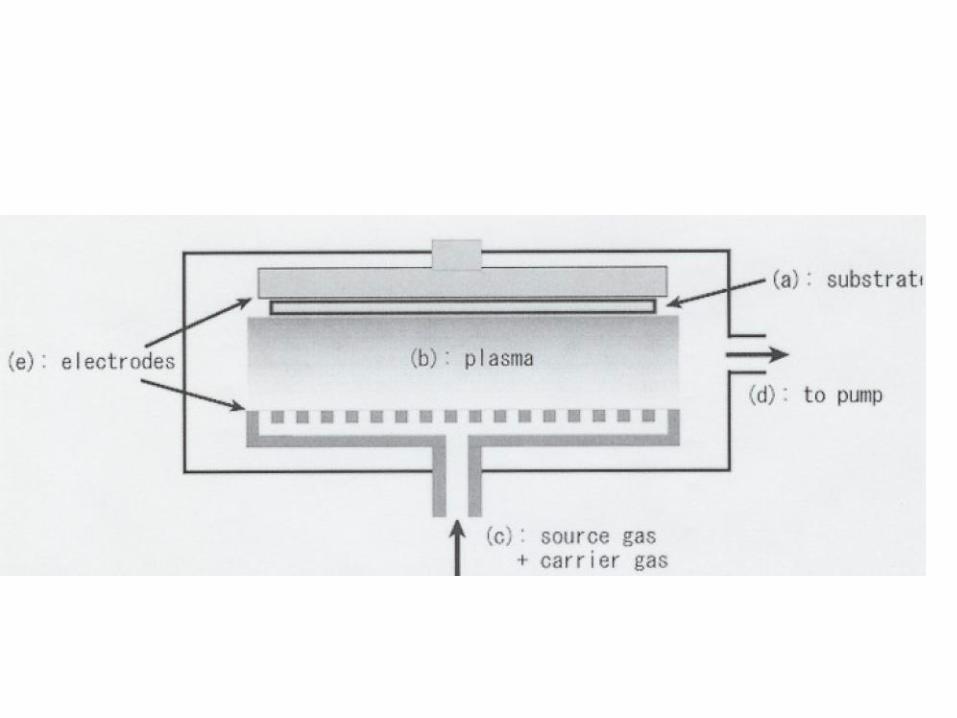
• a-Si:H Discovered in 1970’s
• Made by CVD from SiH4
http://www.solarnavigator.net/images/uni_solar_triple_junction_flexible_cell.jpg
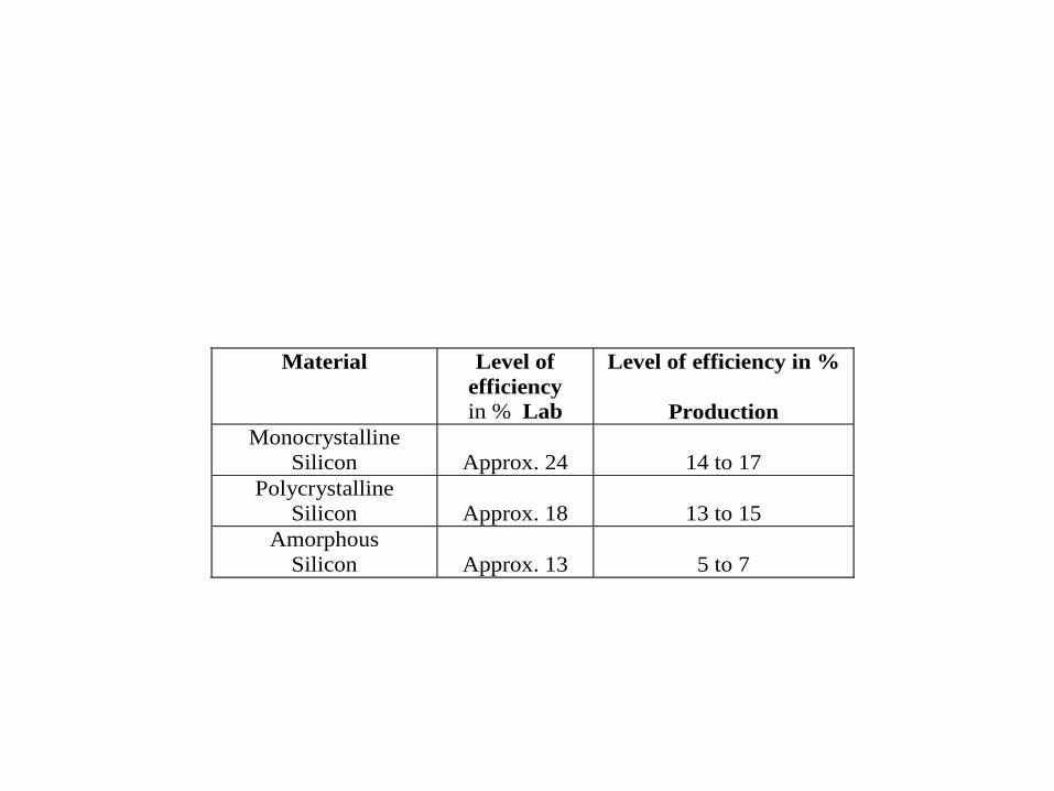
Material Level of
efficiency
in % Lab
Level of efficiency in %
Production
Monocrystalline
Silicon
Approx. 24
14 to 17
Polycrystalline
Silicon
Approx. 18
13 to 15
Amorphous
Silicon
Approx. 13
5 to 7
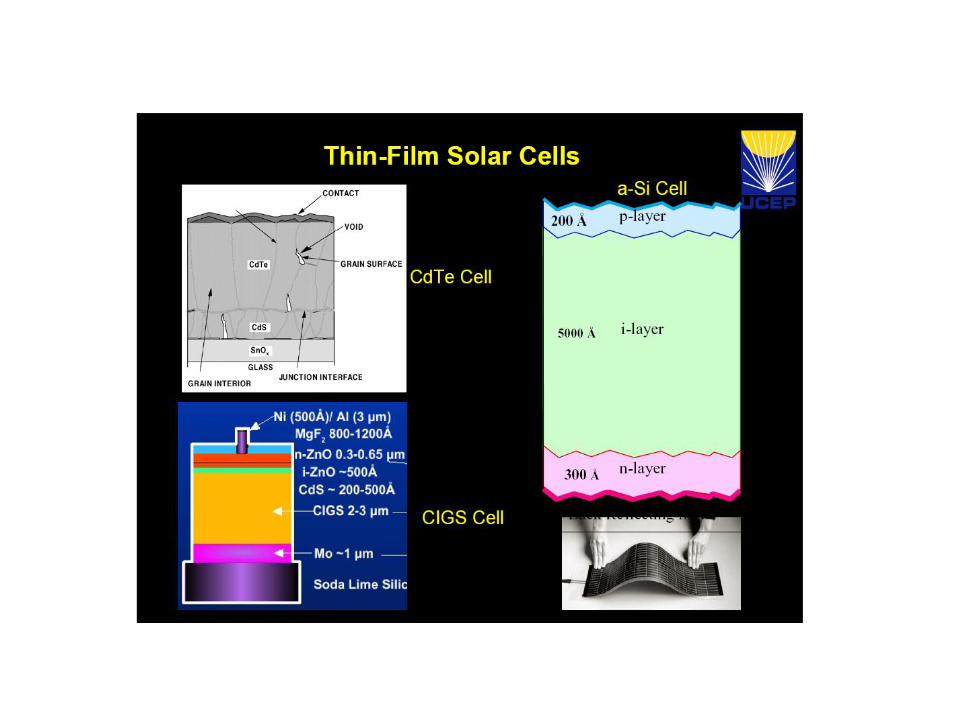
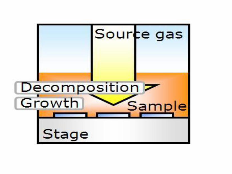
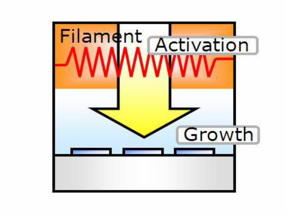
Amorphous Silicon Growth by Thermal CVD
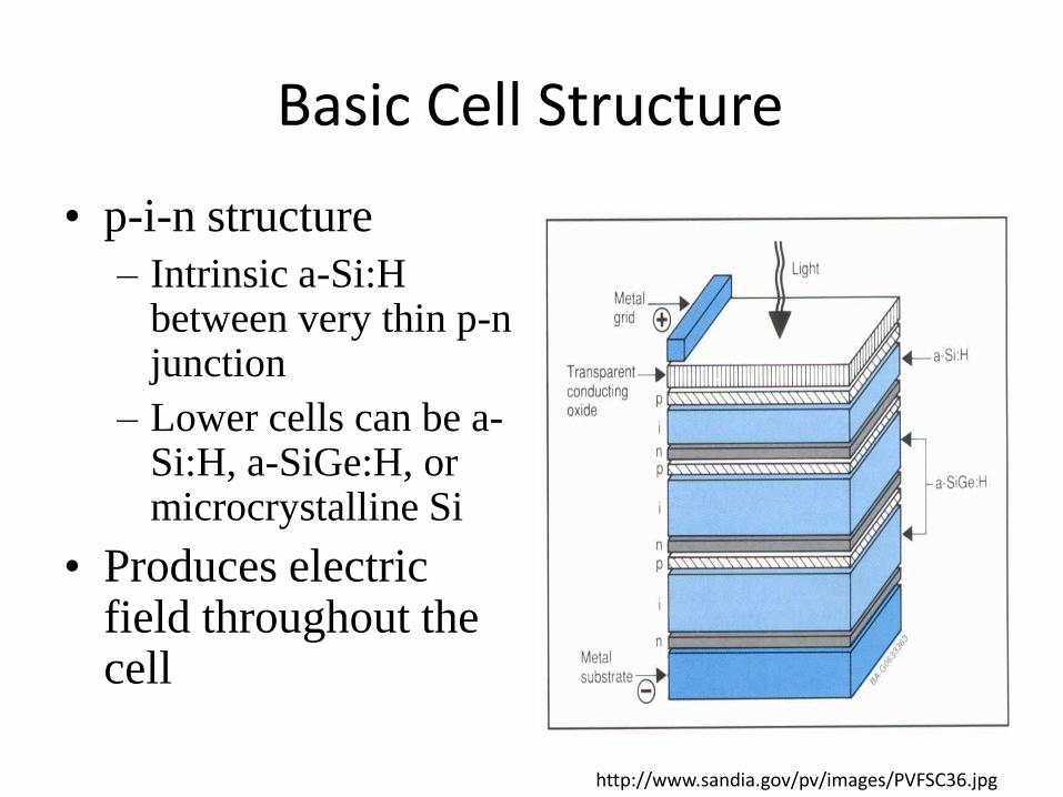
Basic Cell Structure
• p-i-n structure
– Intrinsic a-Si:H between very thin p-n junction
– Lower cells can be a-Si:H, a-SiGe:H, or microcrystalline Si
• Produces electric field throughout the cell
http://www.sandia.gov/pv/images/PVFSC36.jpg
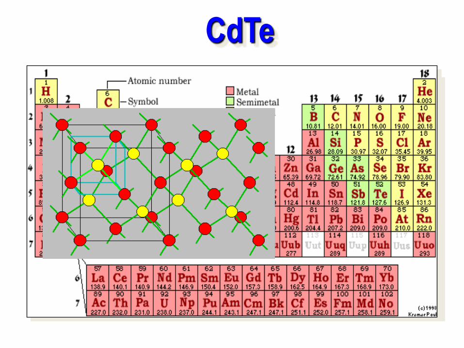
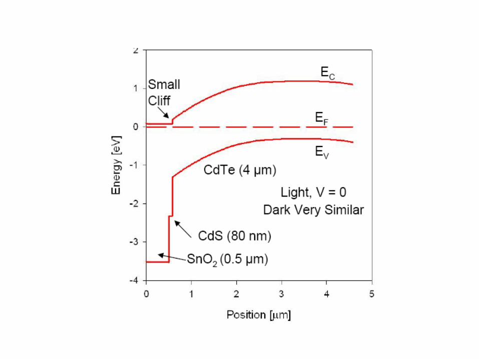
CdTe
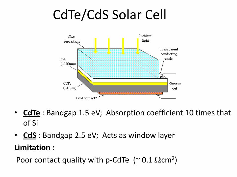
CdTe/CdS Solar Cell
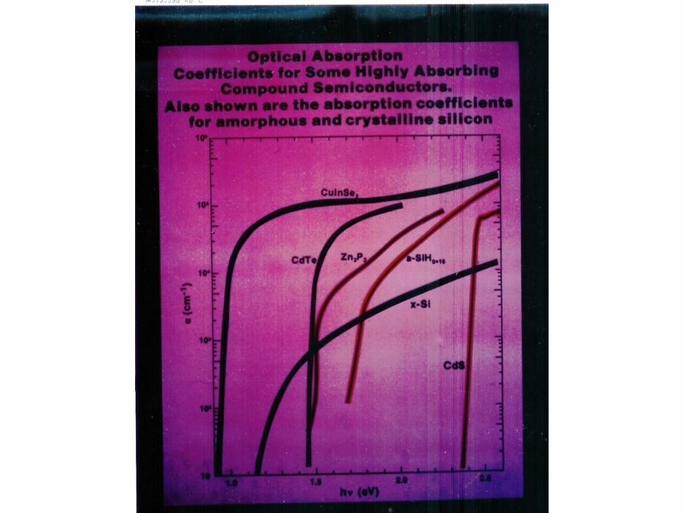
• CdTe : Bandgap 1.5 eV; Absorption coefficient 10 times that of Si
• CdS : Bandgap 2.5 eV; Acts as window layer
Limitation :
Poor contact quality with p-CdTe (~ 0.1 Wcm2)
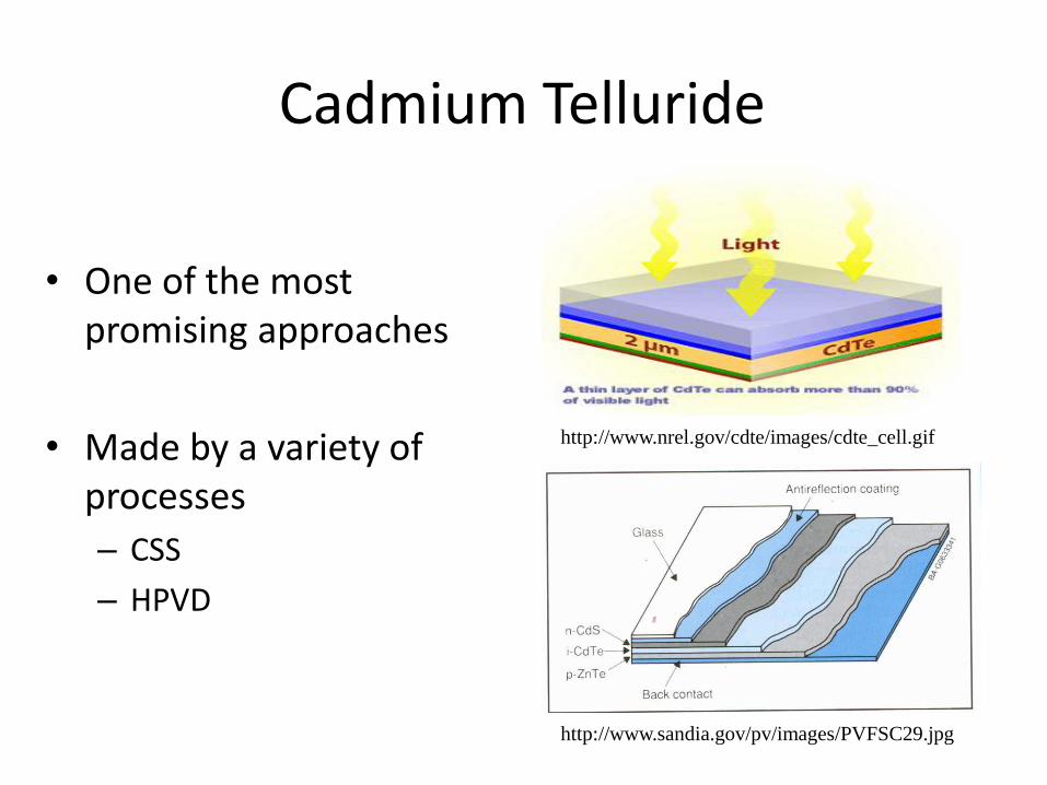
Cadmium Telluride
• One of the most promising approaches
• Made by a variety of processes
– CSS
– HPVD
http://www.nrel.gov/cdte/images/cdte_cell.gif
http://www.sandia.gov/pv/images/PVFSC29.jpg
John A. Woollam, PV talk UNL 2007 31
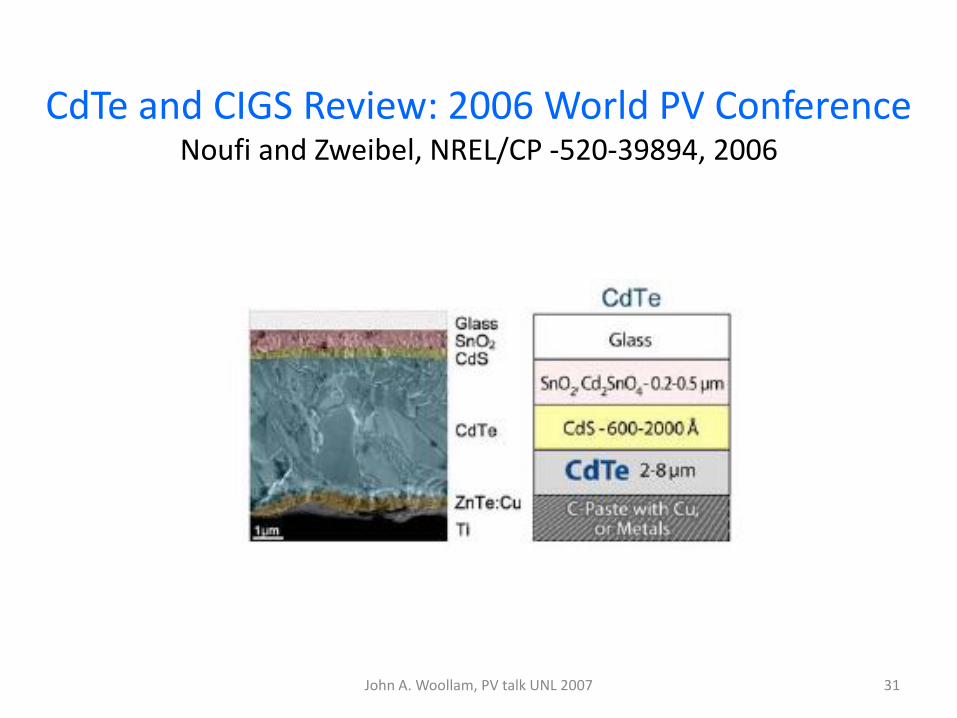
CdTe and CIGS Review: 2006 World PV ConferenceNoufi and Zweibel, NREL/CP -520-39894, 2006
John A. Woollam, PV talk UNL 2007
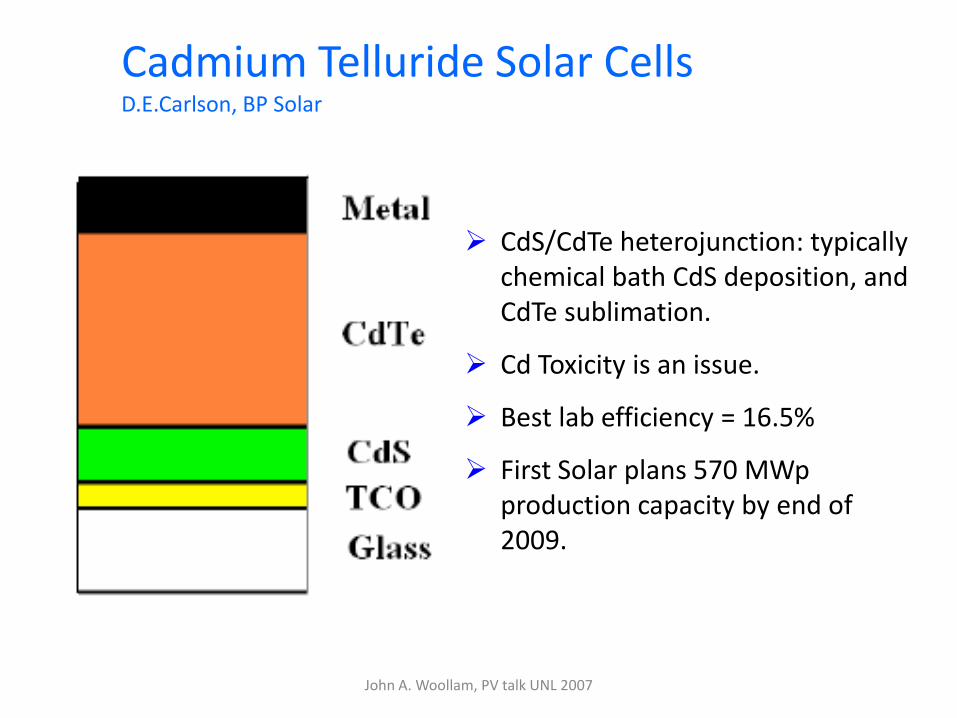
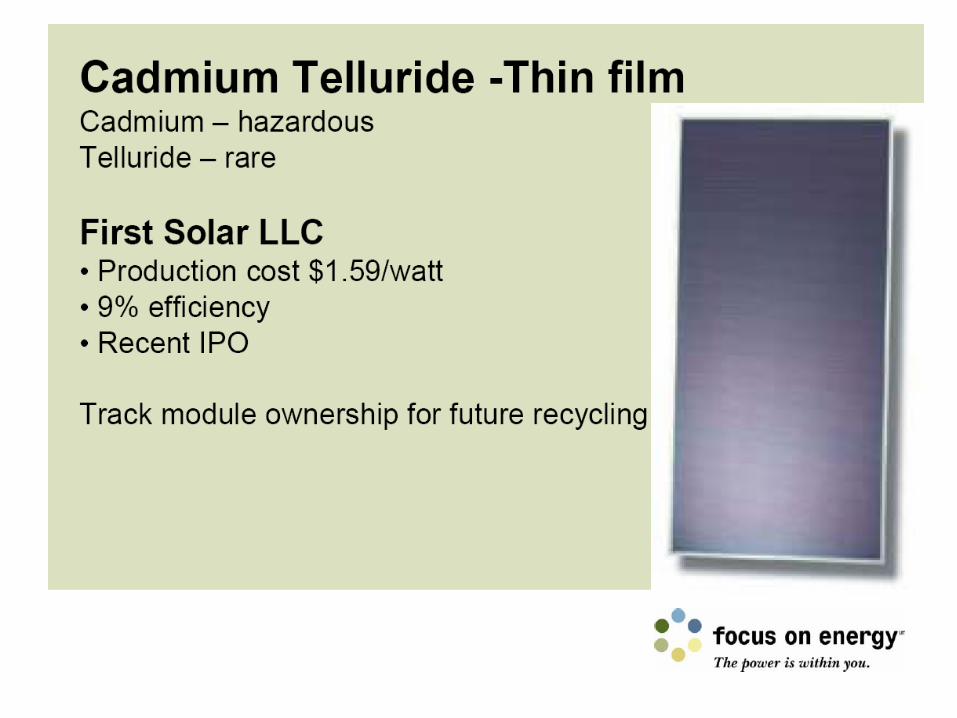
Cadmium Telluride Solar CellsD.E.Carlson, BP Solar
CdS/CdTe heterojunction: typically chemical bath CdS deposition, and CdTe sublimation.
Cd Toxicity is an issue.
Best lab efficiency = 16.5%
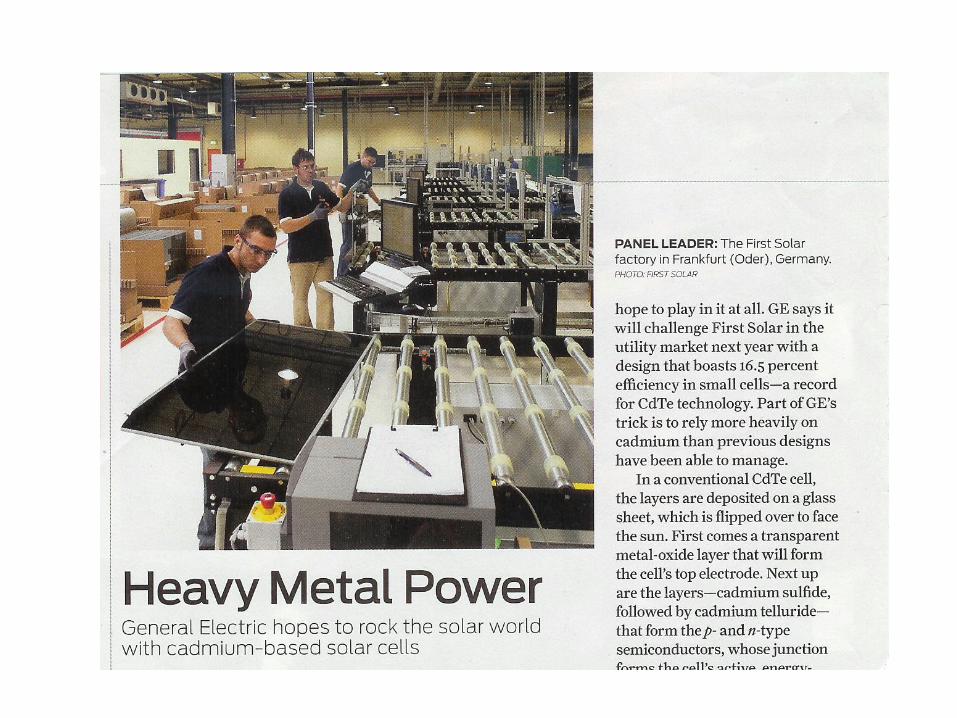
First Solar plans 570 MWp production capacity by end of 2009.
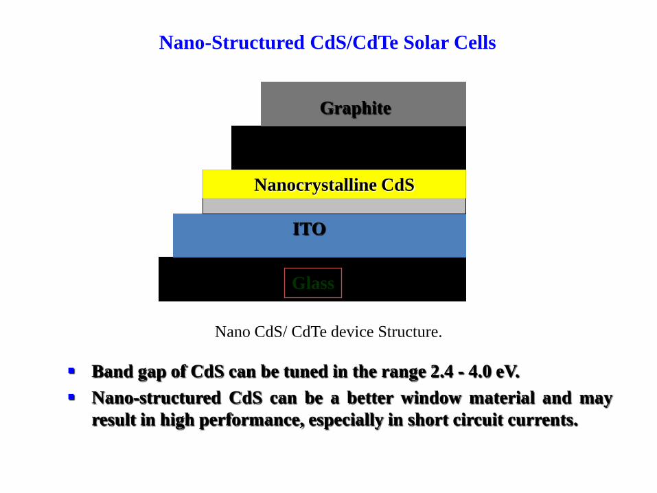
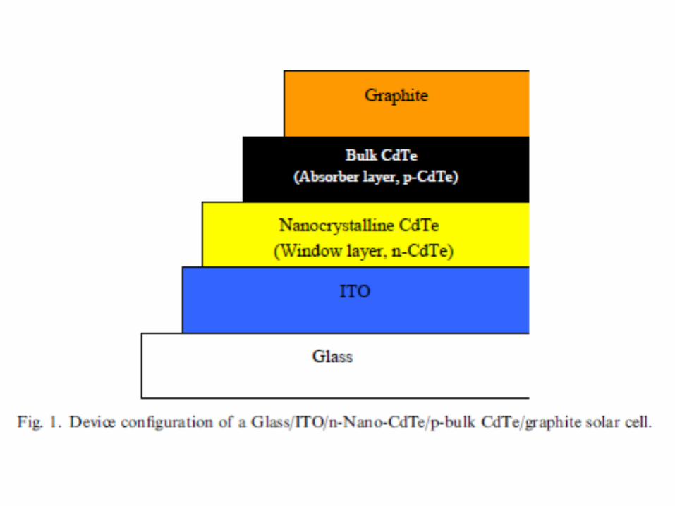
Nano-Structured CdS/CdTe Solar Cells
Nanocrystalline CdS
CdTe
ITO
Glass
Graphite
Band gap of CdS can be tuned in the range 2.4 - 4.0 eV.
Nano-structured CdS can be a better window material and may
result in high performance, especially in short circuit currents.
Nano CdS/ CdTe device Structure.
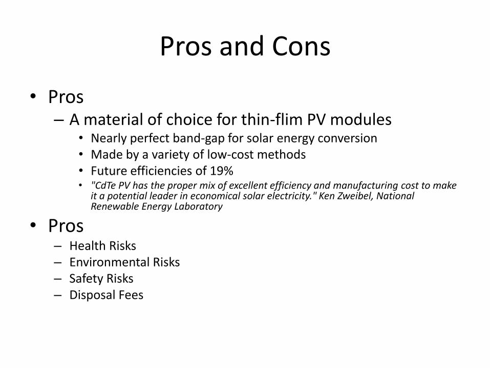
Pros and Cons
• Pros– A material of choice for thin-flim PV modules
• Nearly perfect band-gap for solar energy conversion• Made by a variety of low-cost methods• Future efficiencies of 19%• "CdTe PV has the proper mix of excellent efficiency and manufacturing cost to make
it a potential leader in economical solar electricity." Ken Zweibel, National Renewable Energy Laboratory
• Pros– Health Risks– Environmental Risks– Safety Risks– Disposal Fees
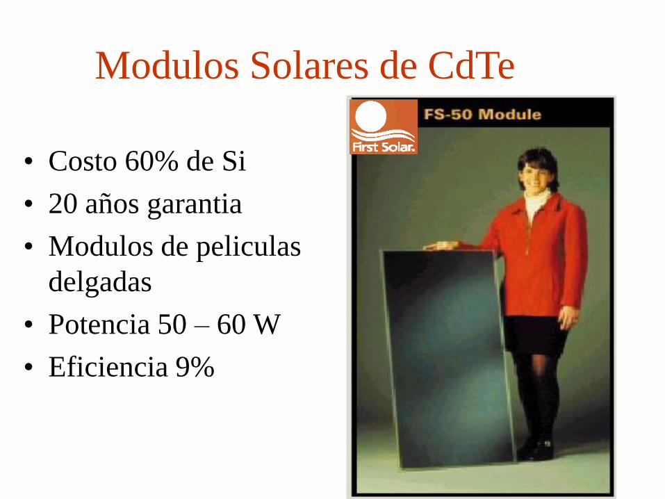
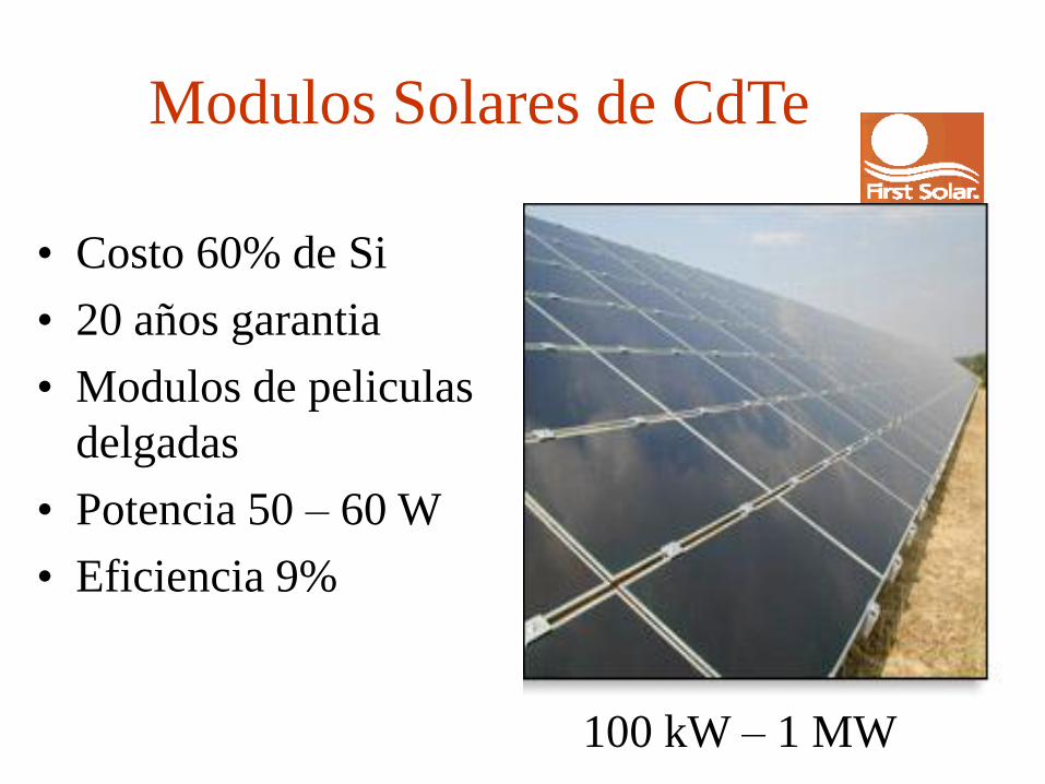
Modulos Solares de CdTe
• Costo 60% de Si
• 20 años garantia
• Modulos de peliculas
delgadas
• Potencia 50 – 60 W
• Eficiencia 9%
Modulos Solares de CdTe
• Costo 60% de Si
• 20 años garantia
• Modulos de peliculas
delgadas
• Potencia 50 – 60 W
• Eficiencia 9%
100 kW – 1 MW
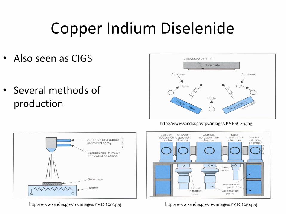
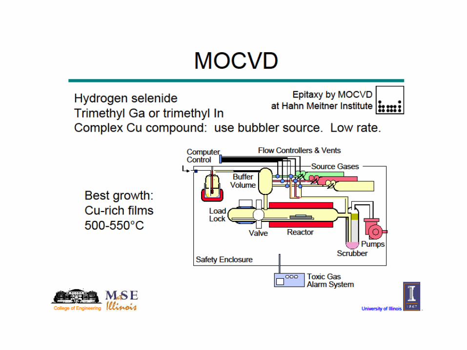
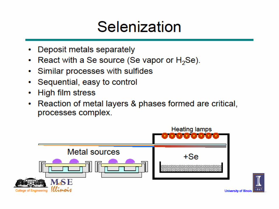
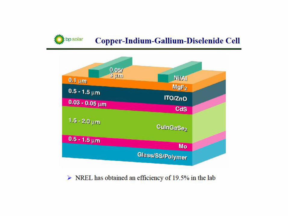
Copper Indium Diselenide
• Also seen as CIGS
• Several methods of production
http://www.sandia.gov/pv/images/PVFSC25.jpg
http://www.sandia.gov/pv/images/PVFSC26.jpghttp://www.sandia.gov/pv/images/PVFSC27.jpg
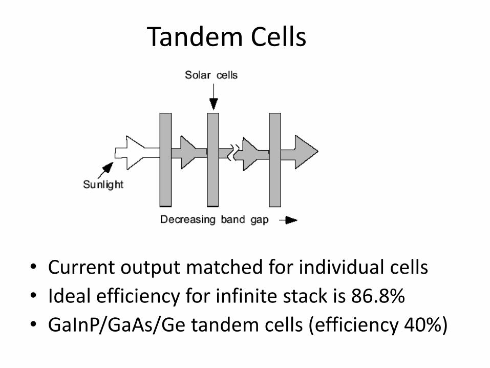
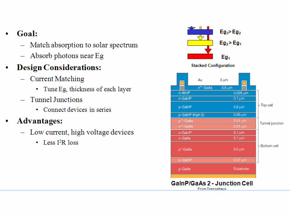
Tandem Cells
• Current output matched for individual cells
• Ideal efficiency for infinite stack is 86.8%
• GaInP/GaAs/Ge tandem cells (efficiency 40%)
6.6.06 - 8.6.06Clemson Summer School
Dr. Karl Molter / FH Trier / [email protected]
49
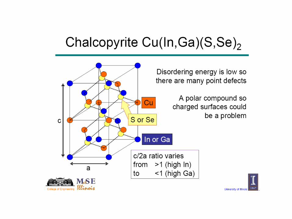
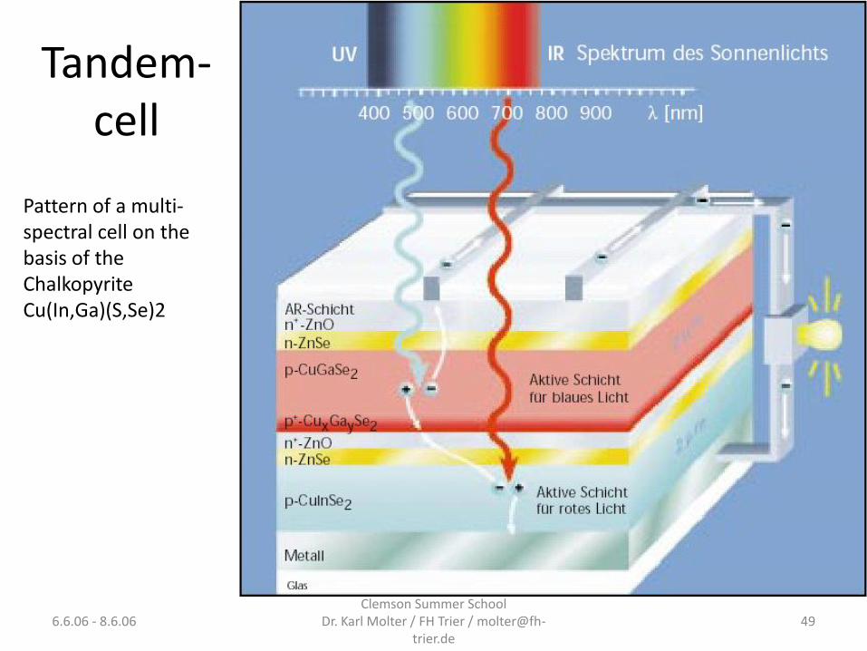
Tandem-cell
Pattern of a multi-spectral cell on the basis of the Chalkopyrite Cu(In,Ga)(S,Se)2
Generation III.
High Efficiency ConcentratorSolar Cells
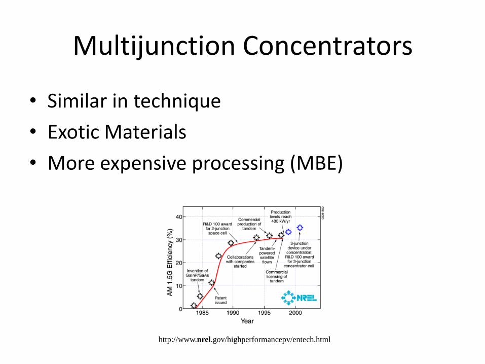
Multijunction Concentrators
• Similar in technique
• Exotic Materials
• More expensive processing (MBE)
http://www.nrel.gov/highperformancepv/entech.html
John A. Woollam, PV talk UNL 2007
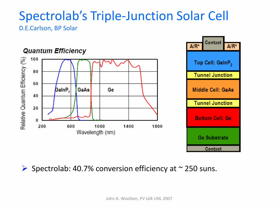
Spectrolab’s Triple-Junction Solar CellD.E.Carlson, BP Solar
Spectrolab: 40.7% conversion efficiency at ~ 250 suns.
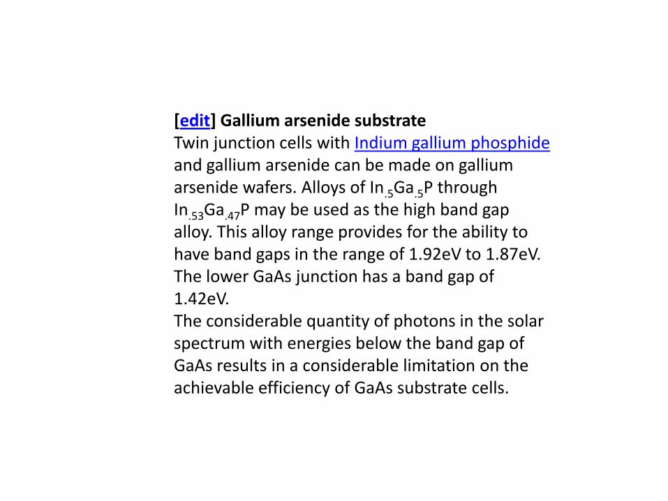
[edit] Gallium arsenide substrateTwin junction cells with Indium gallium phosphideand gallium arsenide can be made on gallium arsenide wafers. Alloys of In.5Ga.5P through In.53Ga.47P may be used as the high band gap alloy. This alloy range provides for the ability to have band gaps in the range of 1.92eV to 1.87eV. The lower GaAs junction has a band gap of 1.42eV.The considerable quantity of photons in the solar spectrum with energies below the band gap of GaAs results in a considerable limitation on the achievable efficiency of GaAs substrate cells.
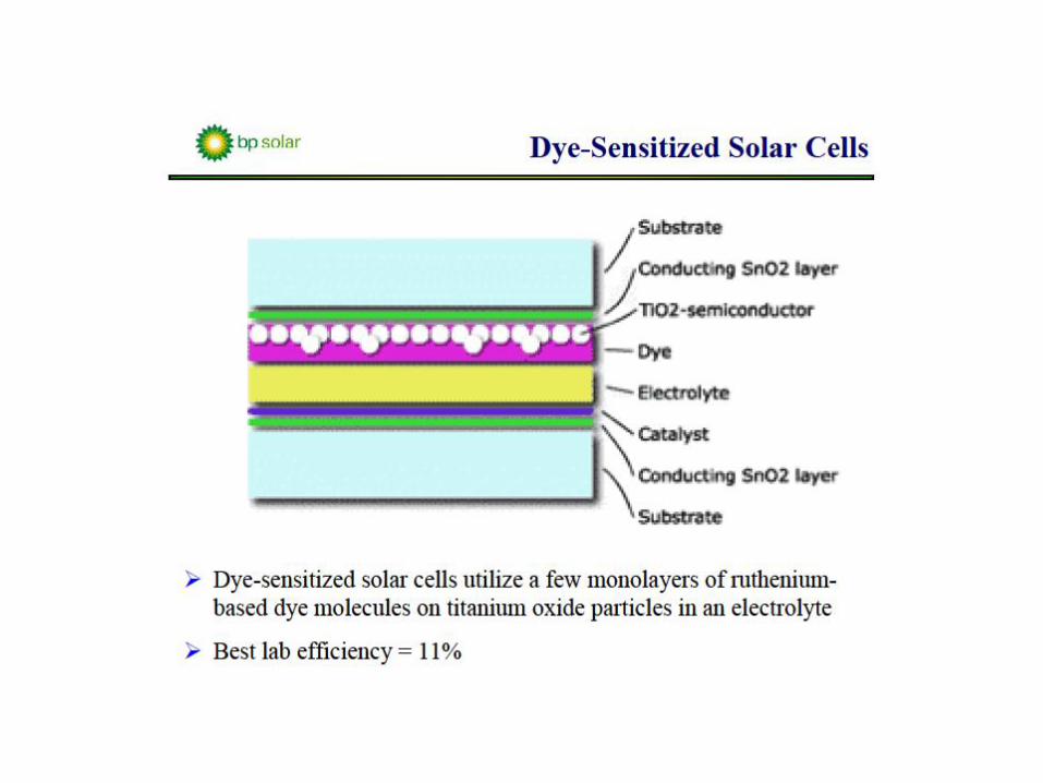
Dye-Sensitized solar cells
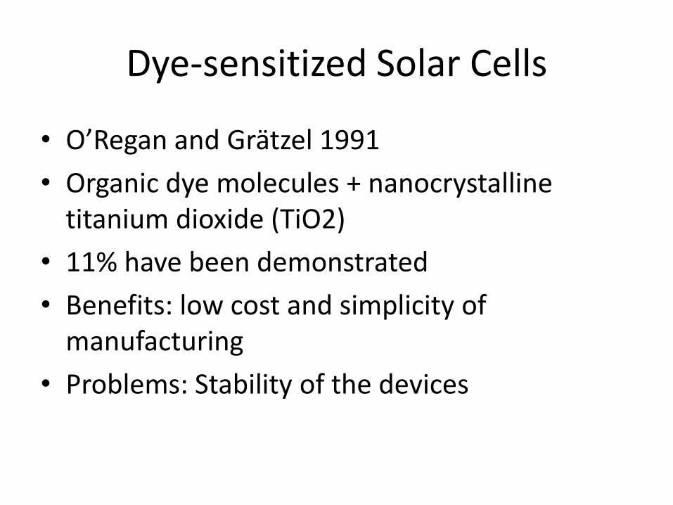
Dye-sensitized Solar Cells
• O’Regan and Grätzel 1991
• Organic dye molecules + nanocrystalline titanium dioxide (TiO2)
• 11% have been demonstrated
• Benefits: low cost and simplicity of manufacturing
• Problems: Stability of the devices
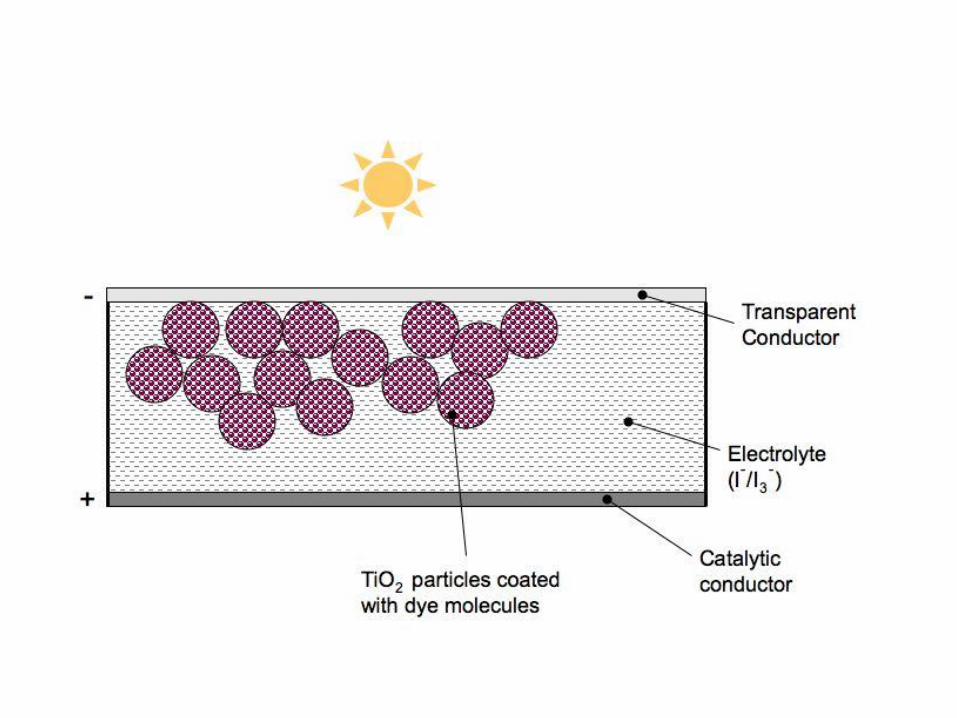
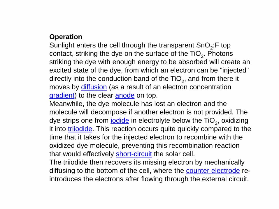
Operation
Sunlight enters the cell through the transparent SnO2:F top
contact, striking the dye on the surface of the TiO2. Photons
striking the dye with enough energy to be absorbed will create an
excited state of the dye, from which an electron can be "injected"
directly into the conduction band of the TiO2, and from there it
moves by diffusion (as a result of an electron concentration
gradient) to the clear anode on top.
Meanwhile, the dye molecule has lost an electron and the
molecule will decompose if another electron is not provided. The
dye strips one from iodide in electrolyte below the TiO2, oxidizing
it into triiodide. This reaction occurs quite quickly compared to the
time that it takes for the injected electron to recombine with the
oxidized dye molecule, preventing this recombination reaction
that would effectively short-circuit the solar cell.
The triiodide then recovers its missing electron by mechanically
diffusing to the bottom of the cell, where the counter electrode re-
introduces the electrons after flowing through the external circuit.
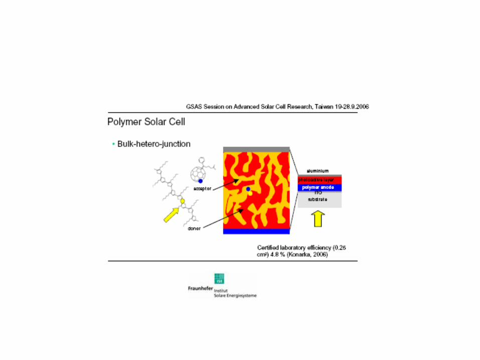
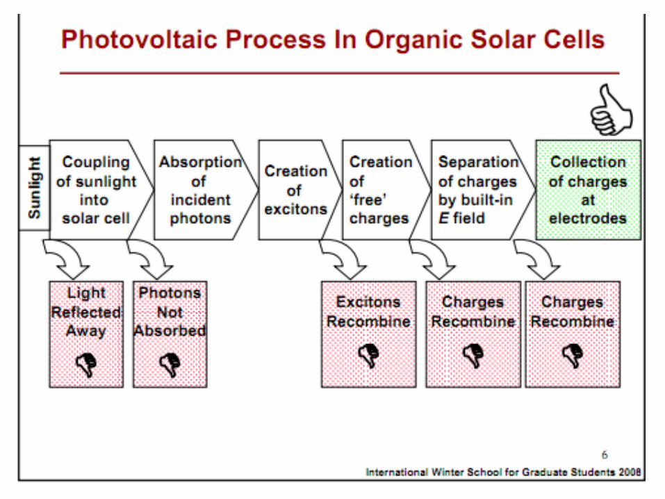
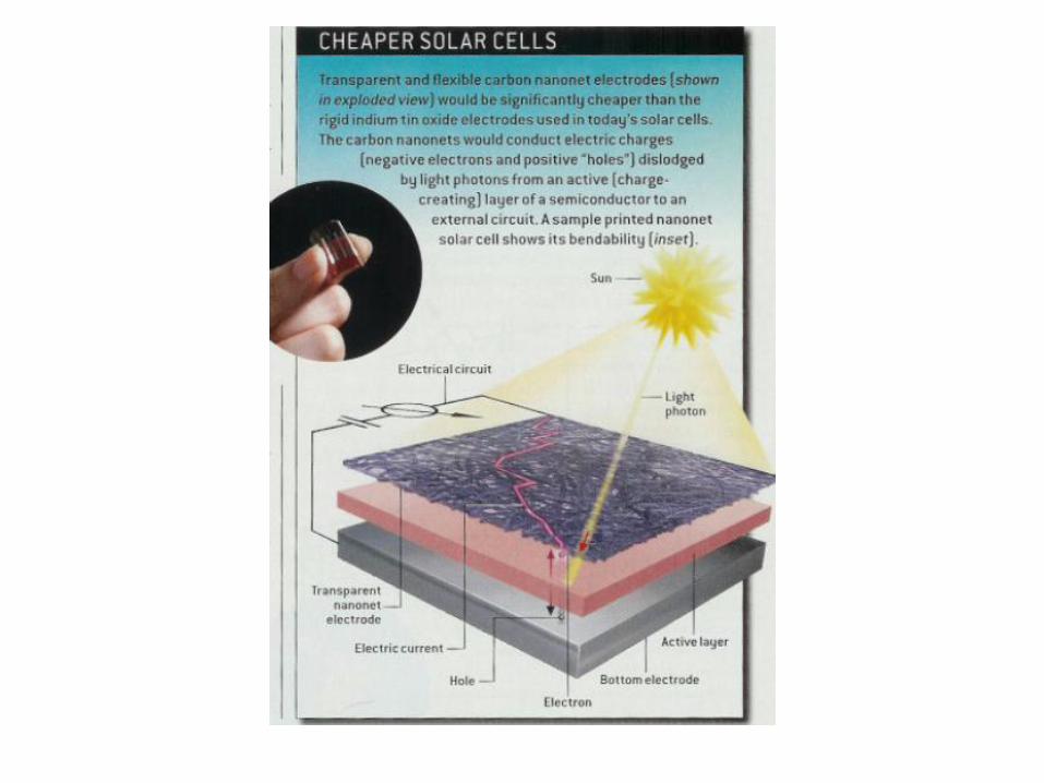
Organic Solar Cells
Organic and Nanotech Solar Cells
Benefits:
• 10 times thinner than thin-film solar cells
• Optical tuning
• Low cost for constituent elements
• High volume production
Problems:
• Current efficiencies < 3-5%
• Long term stability
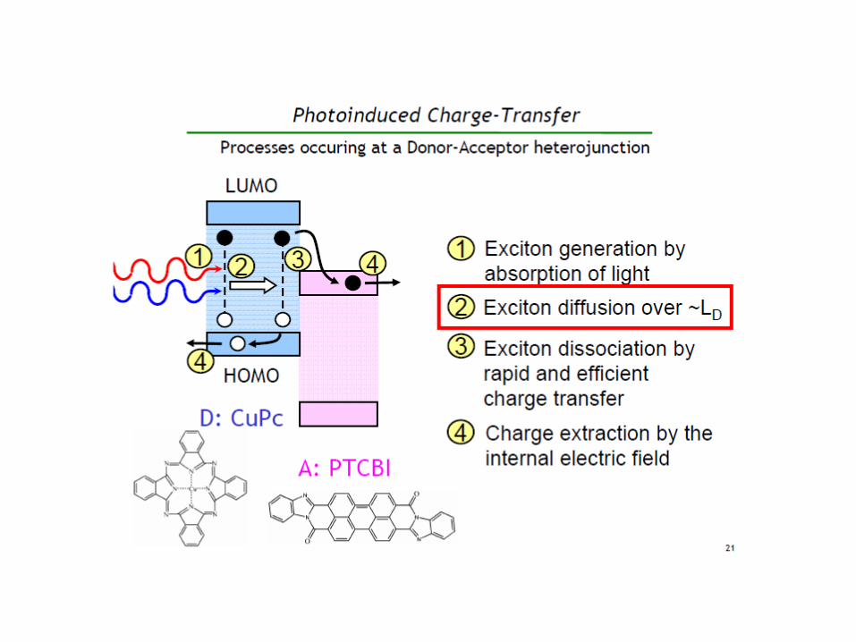
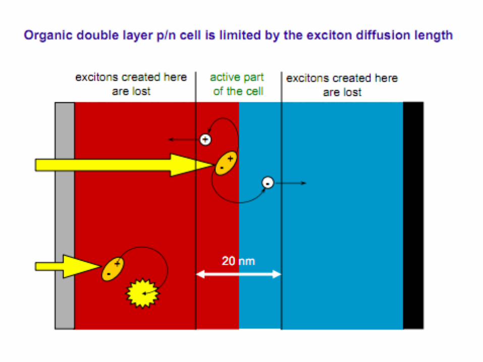
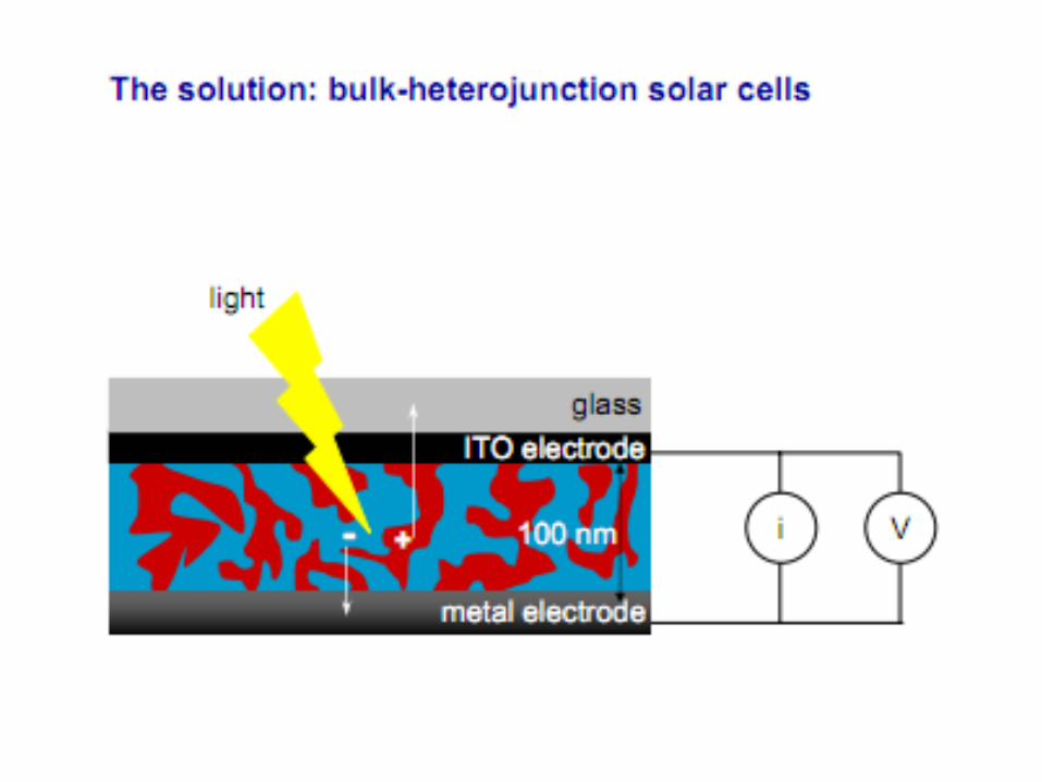
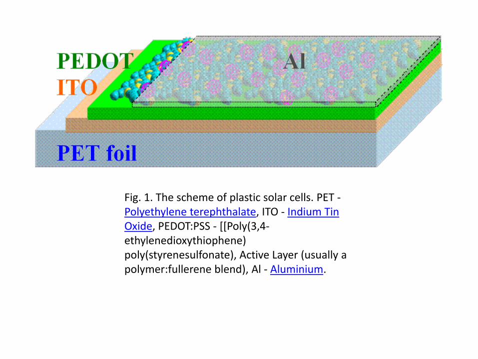
Fig. 1. The scheme of plastic solar cells. PET -Polyethylene terephthalate, ITO - Indium Tin Oxide, PEDOT:PSS - [[Poly(3,4-ethylenedioxythiophene) poly(styrenesulfonate), Active Layer (usually a polymer:fullerene blend), Al - Aluminium.
Nanostructured Solar cells
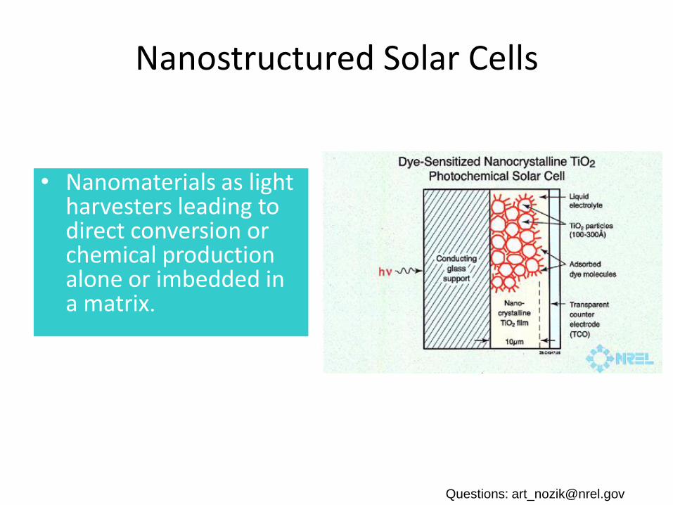
Nanostructured Solar Cells
• Nanomaterials as light harvesters leading to direct conversion or chemical production alone or imbedded in a matrix.
Questions: [email protected]
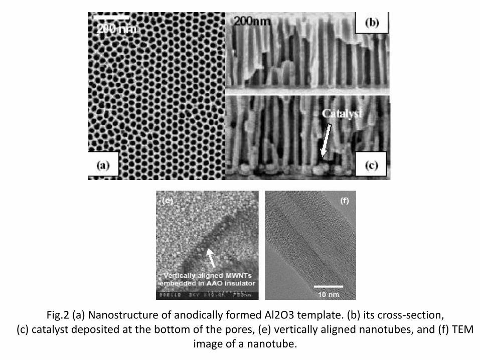
Fig.2 (a) Nanostructure of anodically formed Al2O3 template. (b) its cross-section, (c) catalyst deposited at the bottom of the pores, (e) vertically aligned nanotubes, and (f) TEM
image of a nanotube.
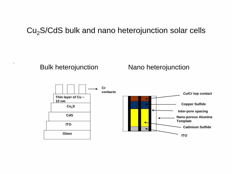
Cu2S/CdS bulk and nano heterojunction solar cells
Glass
ITO
CdS
Cu2S
Thin layer of Cu ~
10 nm
Cr
contacts
Nano-porous Alumina
Template
Inter-pore spacing
ITO
Cadmium Sulfide
Copper Sulfide
Cu/Cr top contact
Bulk heterojunction Nano heterojunction
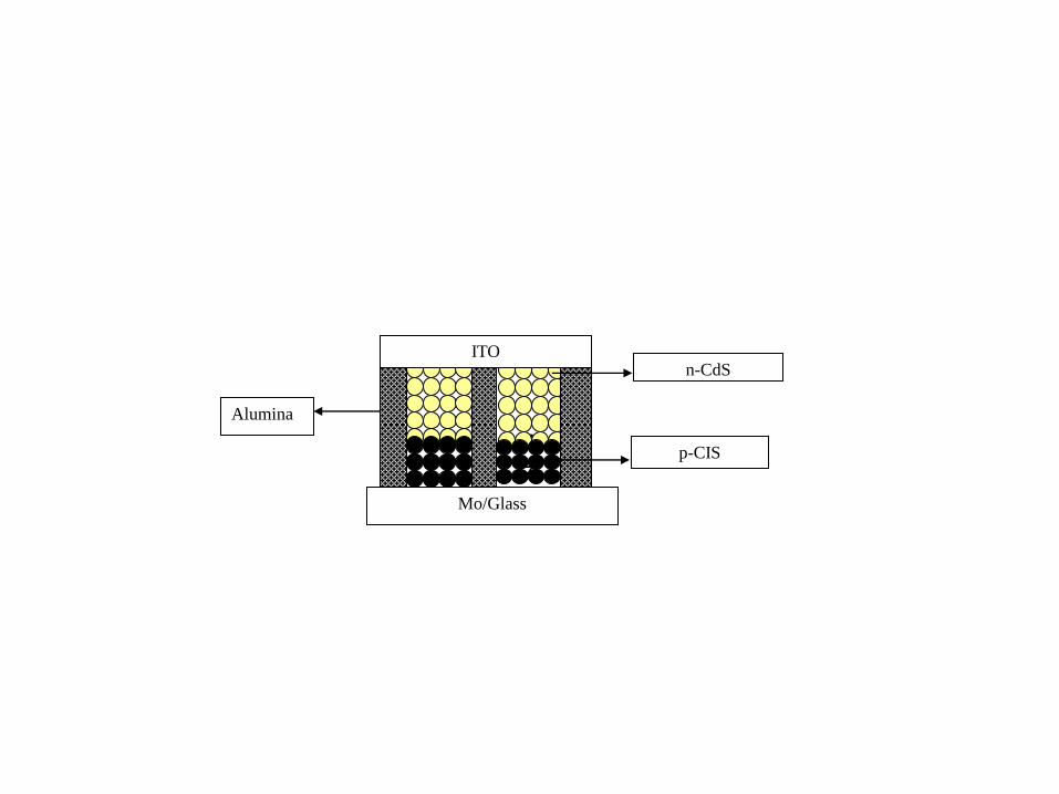
zz
n-CdS
Alumina
p-CIS
Mo/Glass
ITO
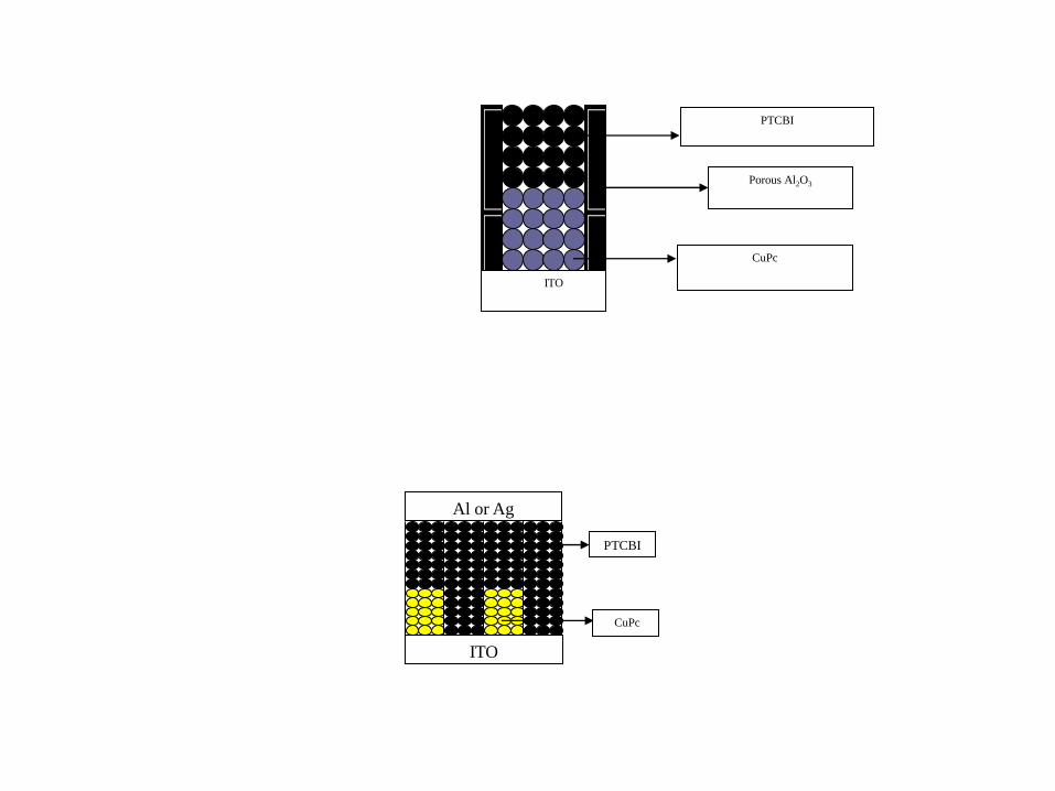
PTCBI
Porous Al2O3
CuPc
ITO
ITO
Al or Ag
CuPc
PTCBI
John A. Woollam, PV talk UNL 2007
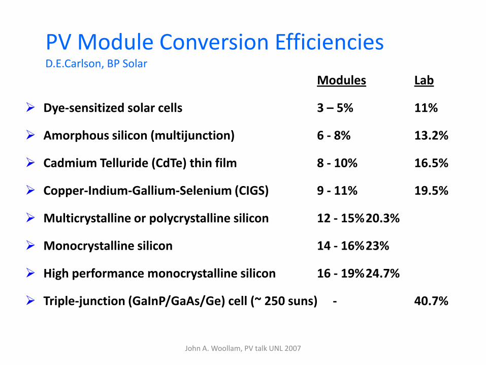
PV Module Conversion EfficienciesD.E.Carlson, BP Solar
Modules Lab
Dye-sensitized solar cells 3 – 5% 11%
Amorphous silicon (multijunction) 6 - 8% 13.2%
Cadmium Telluride (CdTe) thin film 8 - 10% 16.5%
Copper-Indium-Gallium-Selenium (CIGS) 9 - 11% 19.5%
Multicrystalline or polycrystalline silicon 12 - 15%20.3%
Monocrystalline silicon 14 - 16%23%
High performance monocrystalline silicon 16 - 19%24.7%
Triple-junction (GaInP/GaAs/Ge) cell (~ 250 suns) - 40.7%
Generation III Solar Cells not yet realized experimentally
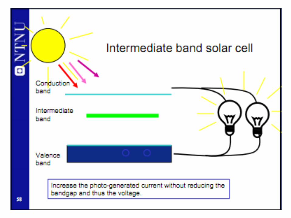
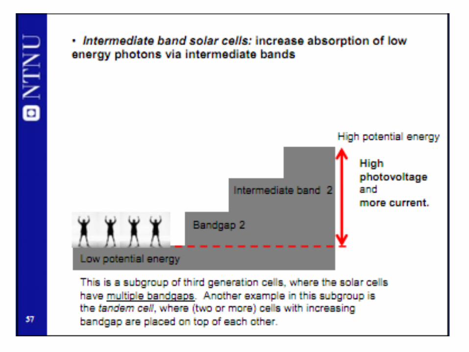
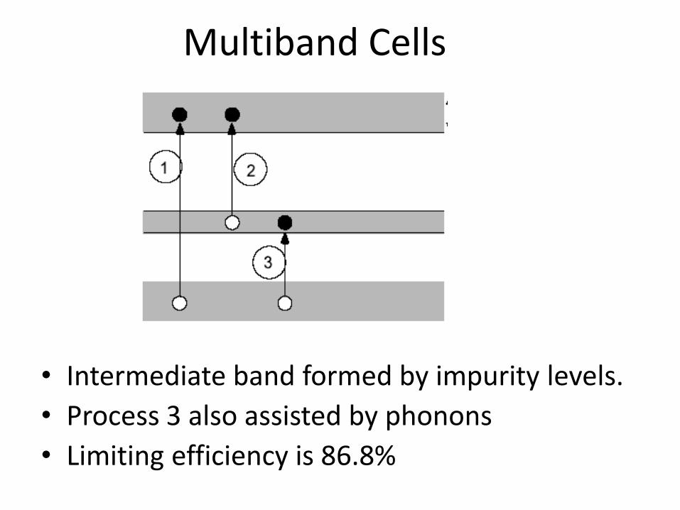
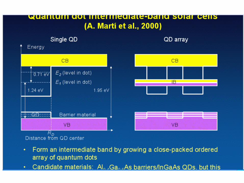
Multiband Cells
• Intermediate band formed by impurity levels.
• Process 3 also assisted by phonons
• Limiting efficiency is 86.8%

Quantum Dots
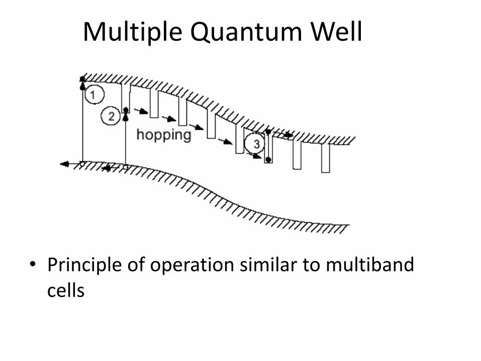
Multiple Quantum Well
• Principle of operation similar to multiband cells
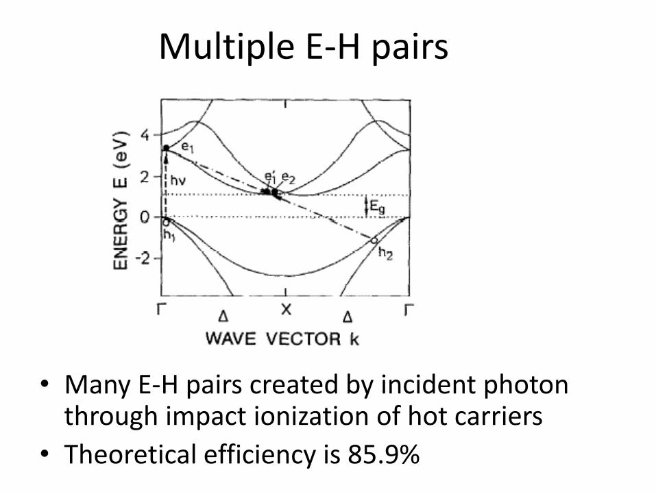
Multiple E-H pairs
• Many E-H pairs created by incident photon through impact ionization of hot carriers
• Theoretical efficiency is 85.9%
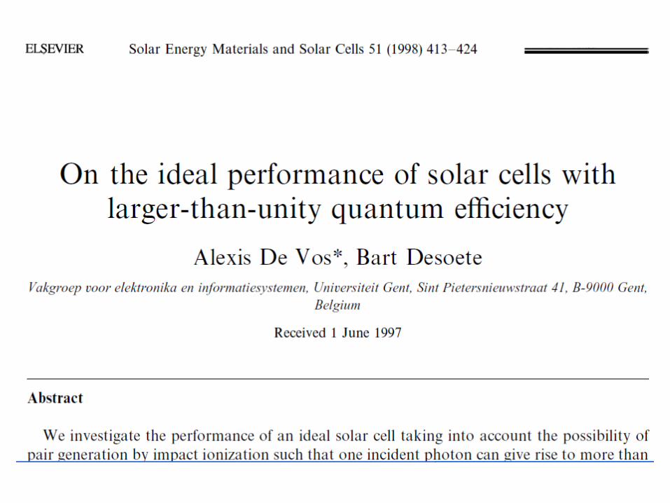
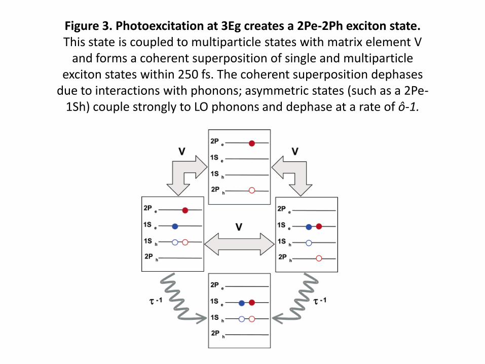
Figure 3. Photoexcitation at 3Eg creates a 2Pe-2Ph exciton state.This state is coupled to multiparticle states with matrix element V
and forms a coherent superposition of single and multiparticleexciton states within 250 fs. The coherent superposition dephases
due to interactions with phonons; asymmetric states (such as a 2Pe-1Sh) couple strongly to LO phonons and dephase at a rate of ô-1.
To study MEG processes in QDs, we detectmultiexcitons created via exciton multiplication (EM) bymonitoring the signature of multiexciton decay in thetransient absorption (TA) dynamics, while maintaining apump photon fluence lower than that needed to createmultiexcitions directly. The Auger recombination rate isproportional to the number of excitons per QD with thedecay of a biexciton being faster than that of the singleexciton. By monitoring the fast-decay component of theTA dynamics at low pump intensities we can measure thepopulation of excitons created by MEG.
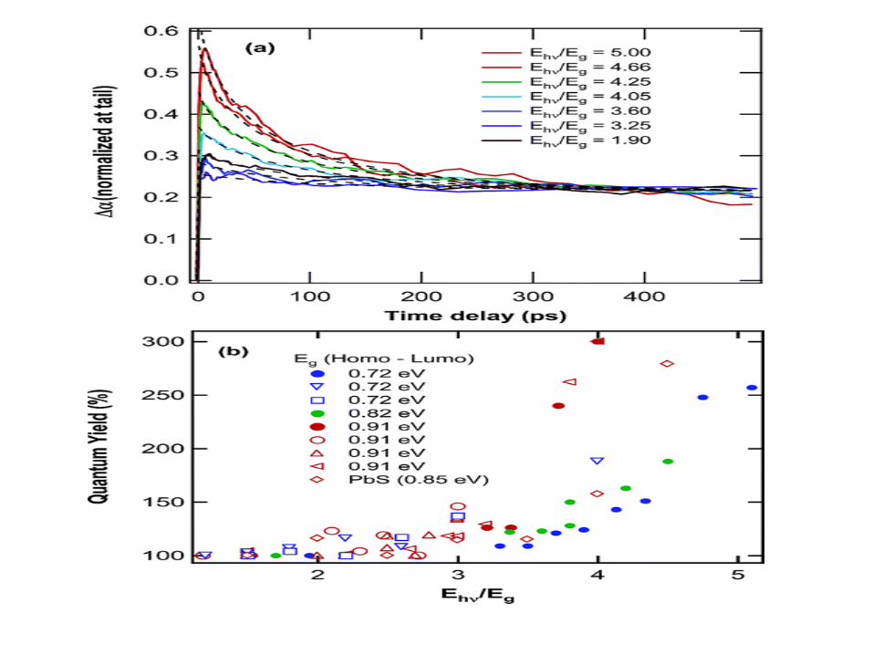
The work reported here provides a confirmation of theprevious report of efficient MEG in PbSe. We observed apreviously unattained 300% QY exciting at 4Eg in PbSe QDs,indicating that we generate an average of three excitons perphoton absorbed. In addition, we present the first knownreport of multiple exciton generation in PbS QDs, at anefficiency comparable to that in PbSe QDs. We have shownthat a single photon with energy larger than 2Eg can generatemultiple excitons in PbSe nanocrystals, and we introduce anew model for MEG based on the coherent superposition ofmultiple excitonic states. Multiple exciton generation incolloidal QDs represents a new and important mechanismthat may greatly increase the conversion efficiency of solarcell devices.
For the 3.9 nm QD (Eg = 0.91 eV), the QY reaches asurprising value of 3.0 at Ehn/Eg = 4. This means that onaverage every QD in the sample produces threeexcitons/photon.
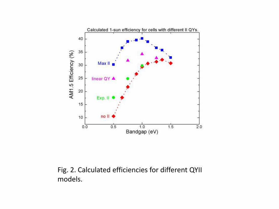
Fig. 2. Calculated efficiencies for different QYII models.