Embed Size (px)
Citation preview
1
Lecture 3: Lithography 1
Prasanna S. GandhiAssistant Professor,Department of Mechanical Engineering,Indian Institute of Technology, Bombay,
MEMS: Fabrication
Recap: Last Class
Applications of MEMS: commercial & researchFabrication processes for MEMS
LithographyMaterial removalMaterial addition
2
Today’s Class
Importance of lithography in VLSI based MEMSFabrication processes for MEMS: Lithography
Various types Optical Lithography
Process detailsImportant parameters
Design considerations:
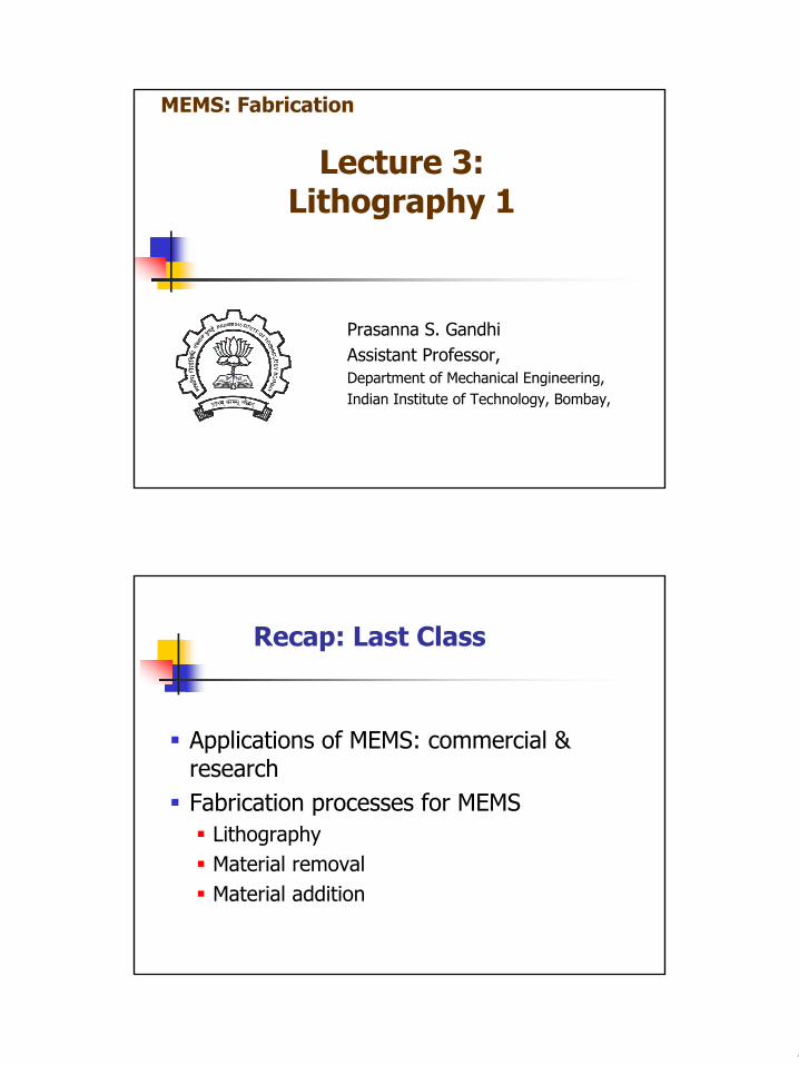
Importance of Lithography
(A) Total Product
Thin Films, 12%
Hot Processes, 16%
Lithography, 32%
Assembly, 15%
Test, 25%
LithographyHot ProcessesThin FilmsAssemblyTest
3
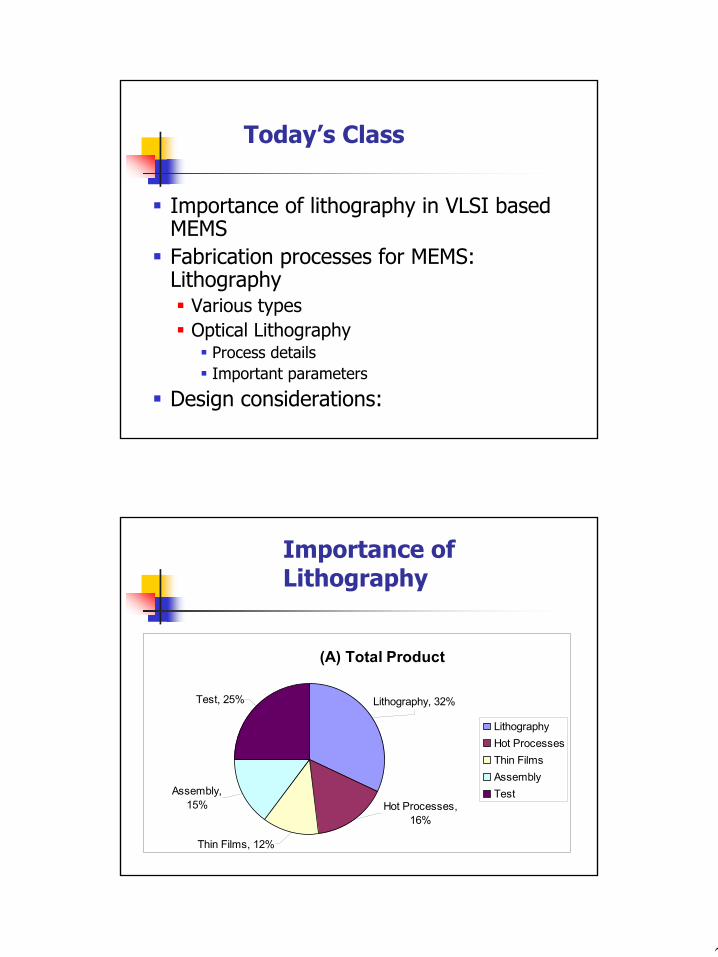
(B) Lithography Manufacturing
Chemicals & Supplies, 40%
Labor & Management,
10%
Equipment & Overhead, 50%
Chemicals & SuppliesLabor & ManagementEquipment & Overhead
Lithography Costs
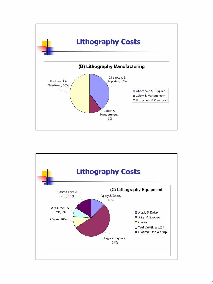
(C) Lithography EquipmentApply & Bake,
12%
Align & Expose, 54%
Clean, 10%
Wet Devel. & Etch, 8%
Plasma Etch & Strip, 16%
Apply & BakeAlign & ExposeCleanWet Devel. & EtchPlasma Etch & Strip
Lithography Costs
4
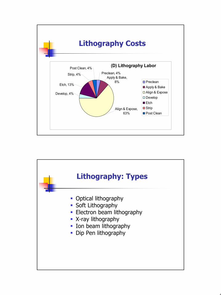
(D) Lithography LaborPreclean, 4%
Apply & Bake, 8%
Strip, 4%
Post Clean, 4%
Etch, 13%
Develop, 4%
Align & Expose, 63%
PrecleanApply & BakeAlign & ExposeDevelopEtchStripPost Clean
Lithography Costs
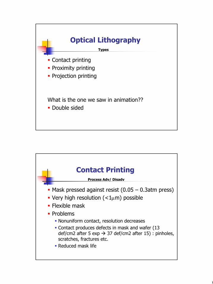
Lithography: Types
Optical lithographySoft Lithography Electron beam lithographyX-ray lithographyIon beam lithographyDip Pen lithography
5
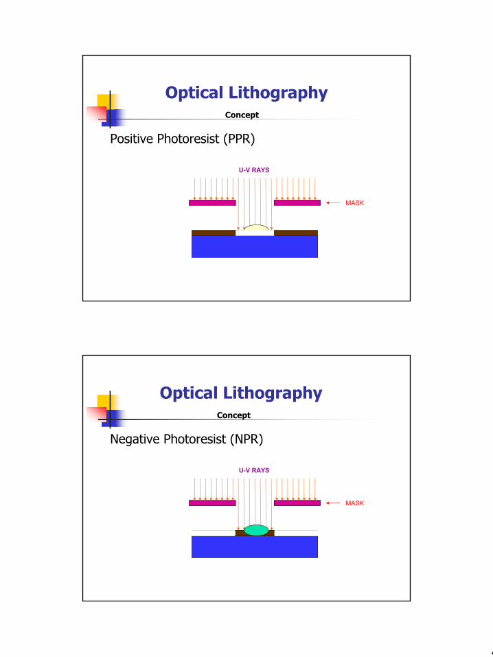
Optical Lithography
Positive Photoresist (PPR)
MASK
U-V RAYS
Concept
Negative Photoresist (NPR)
MASK
U-V RAYS
Concept
Optical Lithography
6
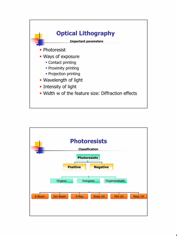
PhotoresistWays of exposure
Contact printingProximity printingProjection printing
Wavelength of lightIntensity of lightWidth w of the feature size: Diffraction effects
Important parameters
Optical Lithography
Classification
Photoresists
Positive
Photoresists
Positive Negative
Photoresist
Organic Inorganic Organometallic
Photoresist
E-Beam Deep UV Mid UVX-RayIon Beam Near UV
7
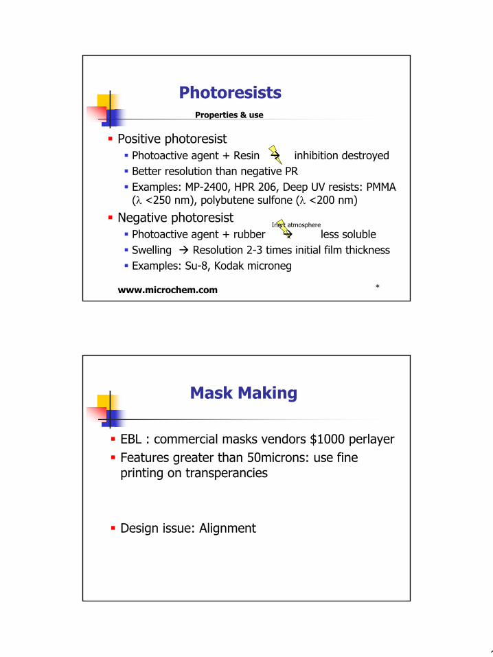
Positive photoresistPhotoactive agent + Resin inhibition destroyedBetter resolution than negative PRExamples: MP-2400, HPR 206, Deep UV resists: PMMA (λ <250 nm), polybutene sulfone (λ <200 nm)
Negative photoresistPhotoactive agent + rubber less solubleSwelling Resolution 2-3 times initial film thicknessExamples: Su-8, Kodak microneg
Properties & use
Photoresists
Inert atmosphere
*www.microchem.com
EBL : commercial masks vendors $1000 perlayerFeatures greater than 50microns: use fine printing on transperancies
Design issue: Alignment
Mask Making
8
Contact printingProximity printingProjection printing
What is the one we saw in animation??Double sided
Types
Optical Lithography
Mask pressed against resist (0.05 – 0.3atm press)Very high resolution (<1µm) possibleFlexible maskProblems
Nonuniform contact, resolution decreasesContact produces defects in mask and wafer (13 def/cm2 after 5 exp 37 def/cm2 after 15) : pinholes, scratches, fractures etc. Reduced mask life
Process Adv/ Disadv
Contact Printing
9
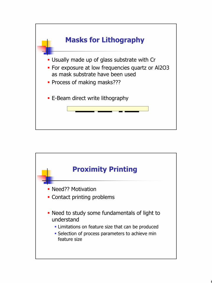
Usually made up of glass substrate with CrFor exposure at low frequencies quartz or Al2O3 as mask substrate have been usedProcess of making masks???
E-Beam direct write lithography
Masks for Lithography
Need?? MotivationContact printing problems
Need to study some fundamentals of light to understand
Limitations on feature size that can be producedSelection of process parameters to achieve min feature size
Proximity Printing
10
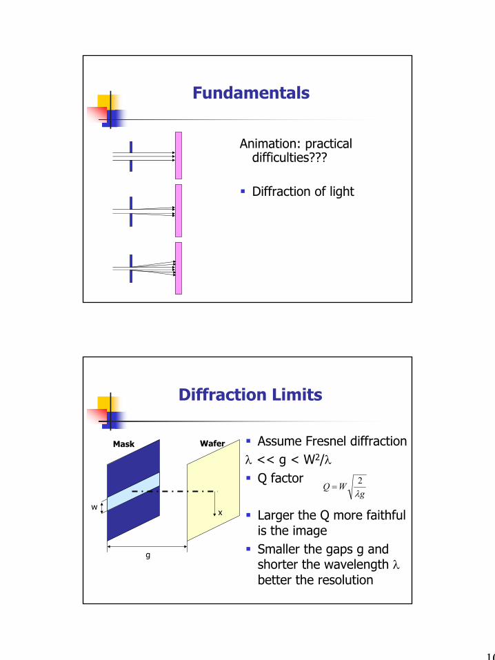
Fundamentals
Animation: practical difficulties???
Diffraction of light
Assume Fresnel diffractionλ << g < W2/λ
Q factor
Larger the Q more faithful is the imageSmaller the gaps g and shorter the wavelength λbetter the resolution
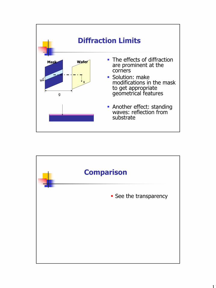
Diffraction Limits
g
xw
Mask Wafer
gWQ
λ2
=
11
The effects of diffraction are prominent at the cornersSolution: make modifications in the mask to get appropriate geometrical features
Another effect: standing waves: reflection from substrate
Diffraction Limits
g
xw
Mask Wafer
Comparison
See the transparency
12
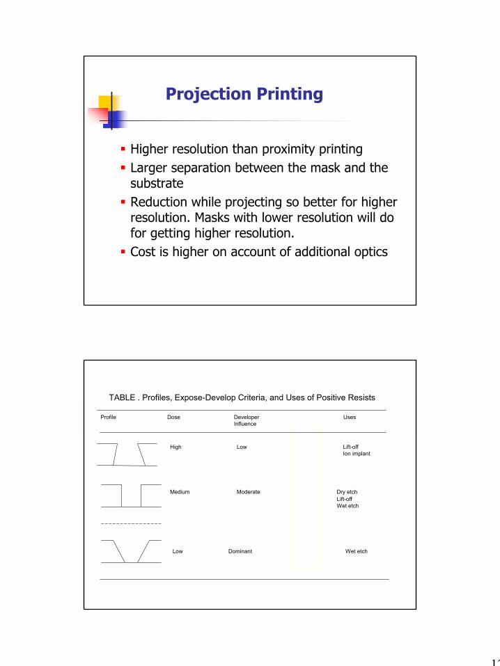
Projection Printing
Higher resolution than proximity printingLarger separation between the mask and the substrateReduction while projecting so better for higher resolution. Masks with lower resolution will do for getting higher resolution.Cost is higher on account of additional optics
TABLE . Profiles, Expose-Develop Criteria, and Uses of Positive Resists
Profile Dose Developer R/Ro UsesInfluence
Low Dominant <5 Wet etch
High Low >10 Lift-offIon implant
Medium Moderate 5-10 Dry etchLift-offWet etch
13
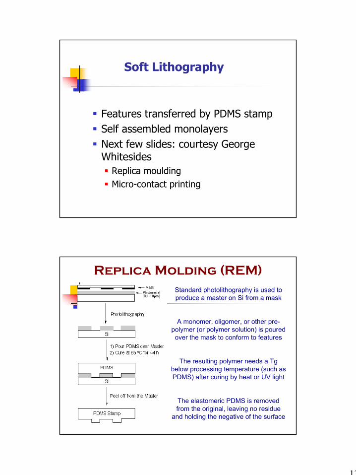
Soft Lithography
Features transferred by PDMS stampSelf assembled monolayersNext few slides: courtesy George Whitesides
Replica mouldingMicro-contact printing
Replica Molding (REM)Standard photolithography is used to produce a master on Si from a mask
A monomer, oligomer, or other pre-polymer (or polymer solution) is poured over the mask to conform to features
The resulting polymer needs a Tgbelow processing temperature (such as PDMS) after curing by heat or UV light
The elastomeric PDMS is removed from the original, leaving no residue
and holding the negative of the surface
14
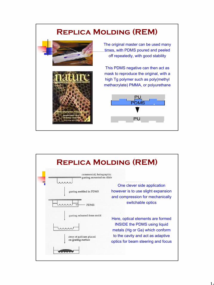
Replica Molding (REM)
The original master can be used many times, with PDMS poured and peeled
off repeatedly, with good stability
This PDMS negative can then act as mask to reproduce the original, with a high Tg polymer such as poly(methyl methacrylate) PMMA, or polyurethane
Replica Molding (REM)
One clever side application however is to use slight expansion and compression for mechanically
switchable optics
Here, optical elements are formed INSIDE the PDMS using liquid
metals (Hg or Ga) which conform to the cavity and act as adaptive
optics for beam steering and focus
15
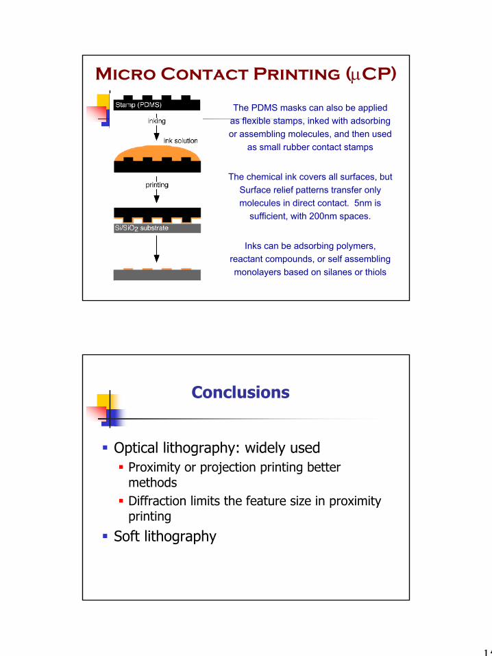
Micro Contact Printing (µCP)
The PDMS masks can also be applied as flexible stamps, inked with adsorbing or assembling molecules, and then used
as small rubber contact stamps
The chemical ink covers all surfaces, but Surface relief patterns transfer only molecules in direct contact. 5nm is
sufficient, with 200nm spaces.
Inks can be adsorbing polymers, reactant compounds, or self assembling monolayers based on silanes or thiols
Conclusions
Optical lithography: widely usedProximity or projection printing better methodsDiffraction limits the feature size in proximity printing
Soft lithography
16
Next class
E beam lithographyChemical etching


![A Thesis Engineering By - Nahrain University · 2018. 6. 4. · gravure, planographic or lithography, and stencil or screen printing [34]. SCREEN PRINTING INK: These inks, often known](https://img.pdfslide.us/doc/110x75/6127743edab1422f1644e568/a-thesis-engineering-by-nahrain-university-2018-6-4-gravure-planographic.jpg)