Embed Size (px)
DESCRIPTION
Lecture #29 CMOS fabrication, clocked and latched circuits. Last lecture: PMOS Physical structure CMOS Dynamic circuits (Ring oscillators) This lecture: CMOS fabrication Clocked and latched circuits. CMOS PARAMETERS 3 generations of CMOS. Return. Interconnect layers. - PowerPoint PPT Presentation
Citation preview
11/8/2004 EE 42 fall 2004 lecture 29 1
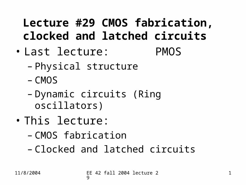
Lecture #29 CMOS fabrication, clocked and latched circuits
• Last lecture: PMOS– Physical structure– CMOS– Dynamic circuits (Ring oscillators)
• This lecture: – CMOS fabrication– Clocked and latched circuits
11/8/2004 EE 42 fall 2004 lecture 29 2
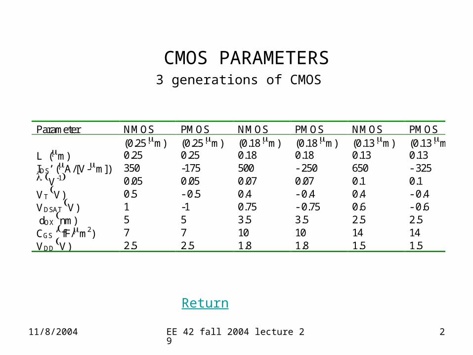
CMOS PARAMETERS3 generations of CMOS
Return
Parameter NMOS PMOS NMOS PMOS NMOS PMOS (0.25m) (0.25m) (0.18m) (0.18m) (0.13m) (0.13m) L (m) 0.25 0.25 0.18 0.18 0.13 0.13 IDS’ (A/[V-m]) 350 -175 500 - 250 650 - 325 V-1 0.05 0.05 0.07 0.07 0.1 0.1 VT
V) 0.5 - 0.5 0.4 - 0.4 0.4 - 0.4 VDSAT
V) 1 -1 0.75 - 0.75 0.6 - 0.6 dOX
nm) 5 5 3.5 3.5 2.5 2.5 CGS ‘fF/m2) 7 7 10 10 14 14 VDD
V) 2.5 2.5 1.8 1.8 1.5 1.5
11/8/2004 EE 42 fall 2004 lecture 29 3
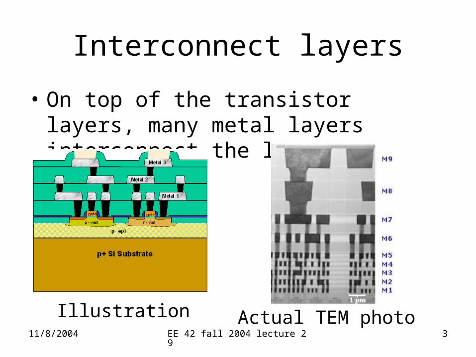
Interconnect layers
• On top of the transistor layers, many metal layers interconnect the logic
Illustration Actual TEM photo
11/8/2004 EE 42 fall 2004 lecture 29 4
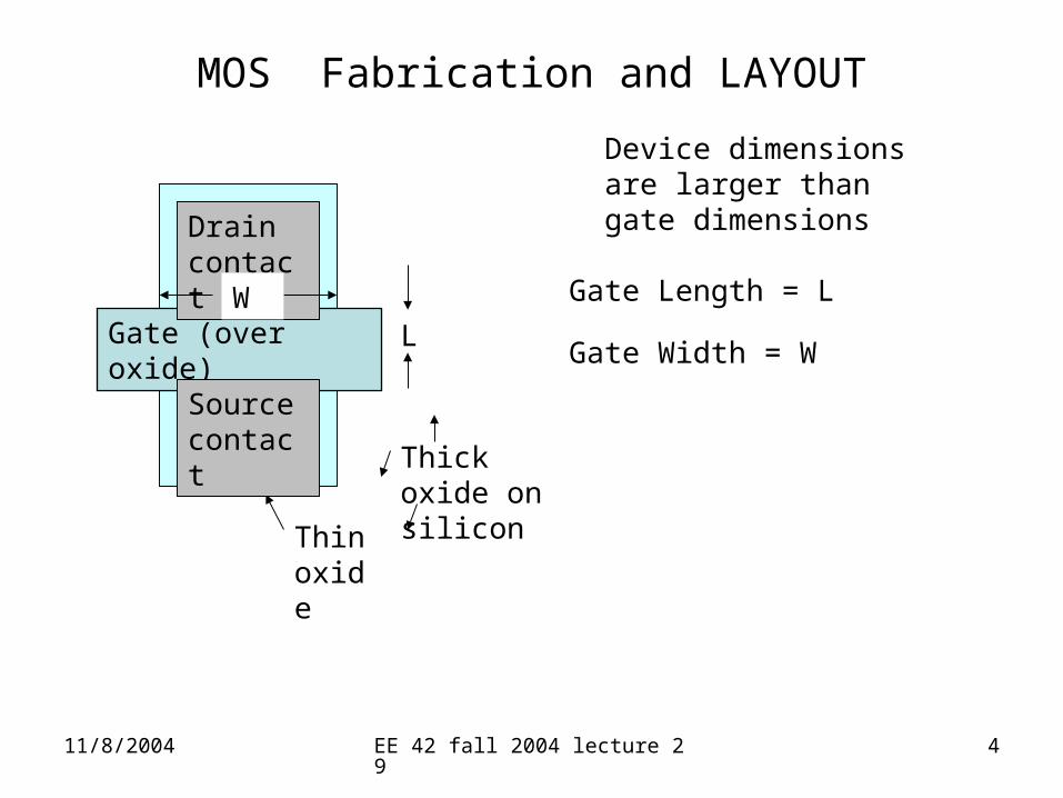
MOS Fabrication and LAYOUT
Thick oxide on silicon
Thin oxide
Gate (over oxide)
Drain contact
Source contact
Device dimensions are larger than gate dimensions
Gate Length = L
Gate Width = WL
W
11/8/2004 EE 42 fall 2004 lecture 29 5
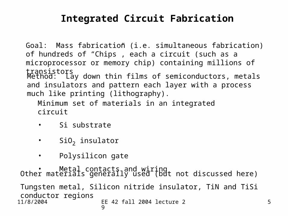
Integrated Circuit Fabrication
Goal: Mass fabrication (i.e. simultaneous fabrication) of hundreds of “Chips”, each a circuit (such as a microprocessor or memory chip) containing millions of transistors
Method: Lay down thin films of semiconductors, metals and insulators and pattern each layer with a process much like printing (lithography).
Minimum set of materials in an integrated circuit
• Si substrate
• SiO2 insulator
• Polysilicon gate
• Metal contacts and wiring
Other materials generally used (but not discussed here)
Tungsten metal, Silicon nitride insulator, TiN and TiSi conductor regions
11/8/2004 EE 42 fall 2004 lecture 29 6
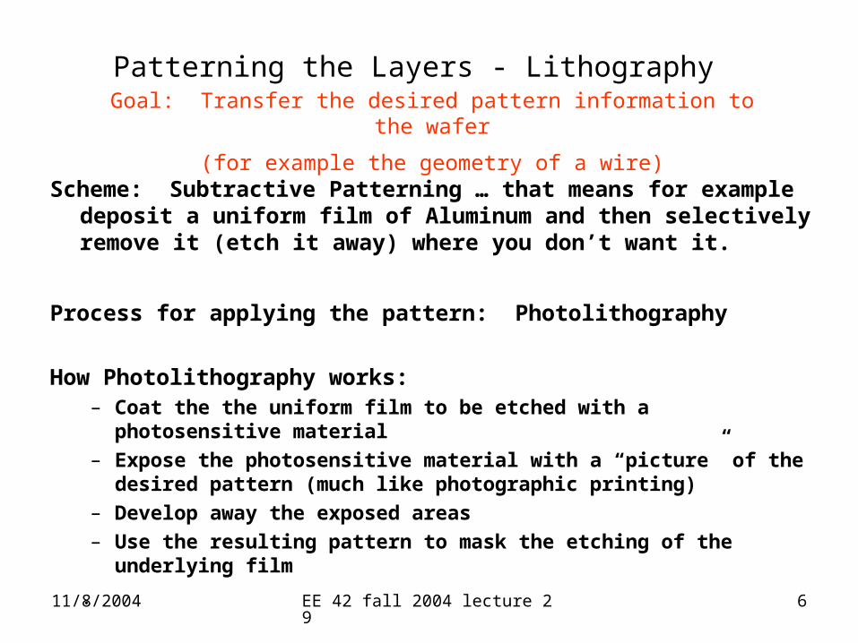
Patterning the Layers - Lithography
Scheme: Subtractive Patterning … that means for example deposit a uniform film of Aluminum and then selectively remove it (etch it away) where you don’t want it.
Process for applying the pattern: Photolithography
How Photolithography works: – Coat the the uniform film to be etched with a photosensitive
material
– Expose the photosensitive material with a “picture” of the desired pattern (much like photographic printing)
– Develop away the exposed areas
– Use the resulting pattern to mask the etching of the underlying film
.
Goal: Transfer the desired pattern information to the wafer
(for example the geometry of a wire)
11/8/2004 EE 42 fall 2004 lecture 29 7
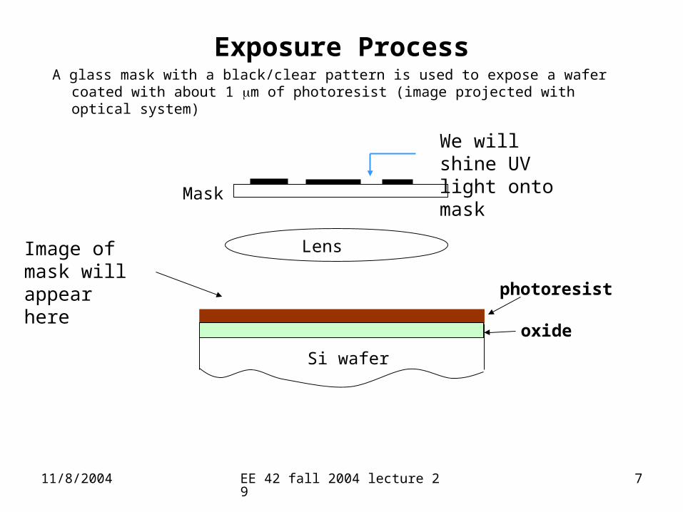
Exposure ProcessA glass mask with a black/clear pattern is used to expose a wafer coated with
about 1 m of photoresist (image projected with optical system)
Mask
LensImage of mask will appear here
We will shine UV light onto mask
Si wafer
photoresist
oxide
11/8/2004 EE 42 fall 2004 lecture 29 8
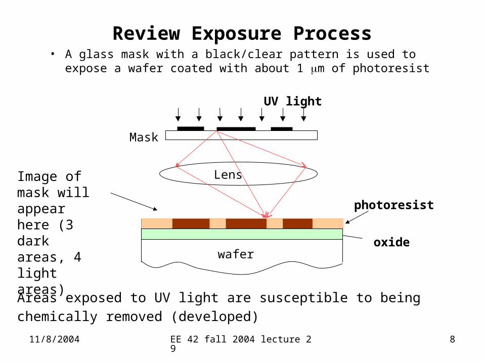
Review Exposure Process• A glass mask with a black/clear pattern is used to expose a
wafer coated with about 1 m of photoresist
Areas exposed to UV light are susceptible to being chemically removed
(developed)
Mask
LensImage of mask will appear here (3 dark areas, 4 light areas)
photoresist
waferoxide
UV light
11/8/2004 EE 42 fall 2004 lecture 29 9
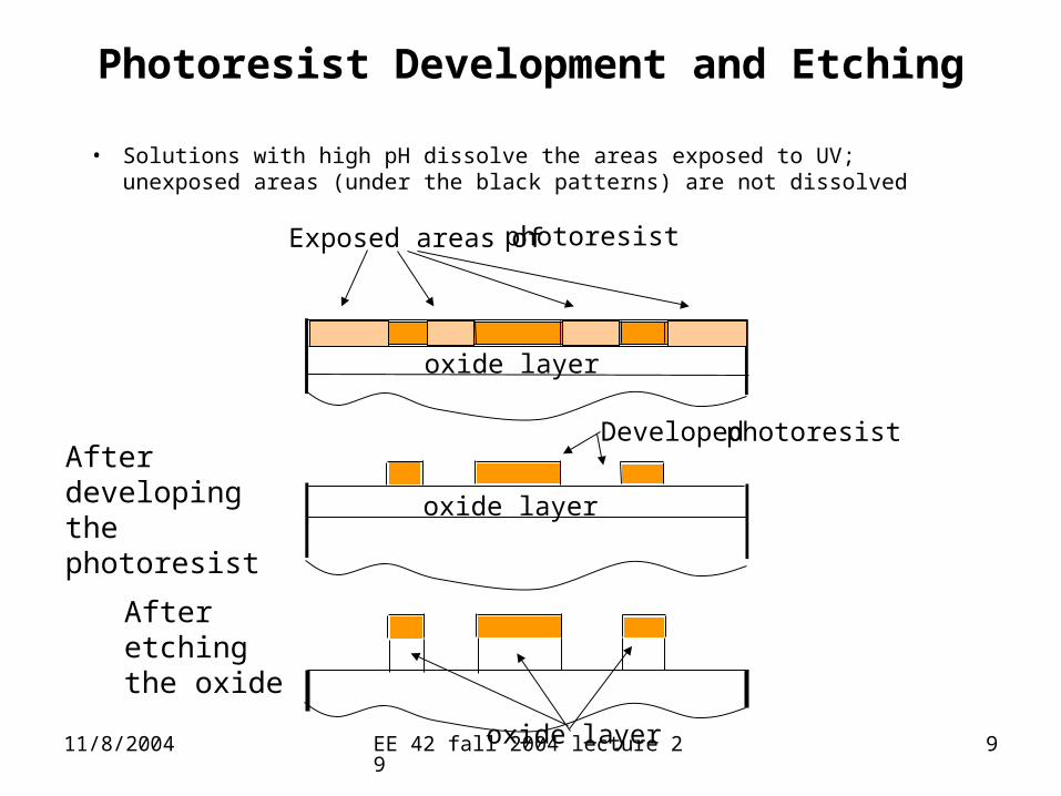
Photoresist Development and Etching
• Solutions with high pH dissolve the areas exposed to UV; unexposed areas (under the black patterns) are not dissolved
oxide layer
After etching the oxide
After developing the photoresist
Developed photoresist
oxide layer
Exposed areas of photoresist
oxide layer
11/8/2004 EE 42 fall 2004 lecture 29 10
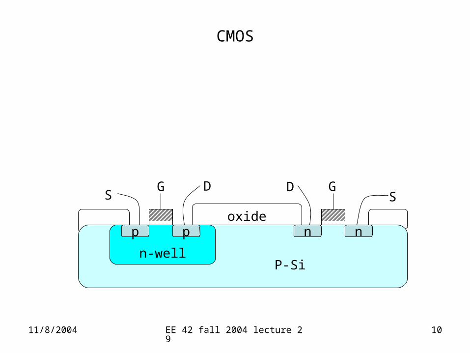
CMOS
oxide
P-Si n-well
p p n n
GDG DSS
11/8/2004 EE 42 fall 2004 lecture 29 11
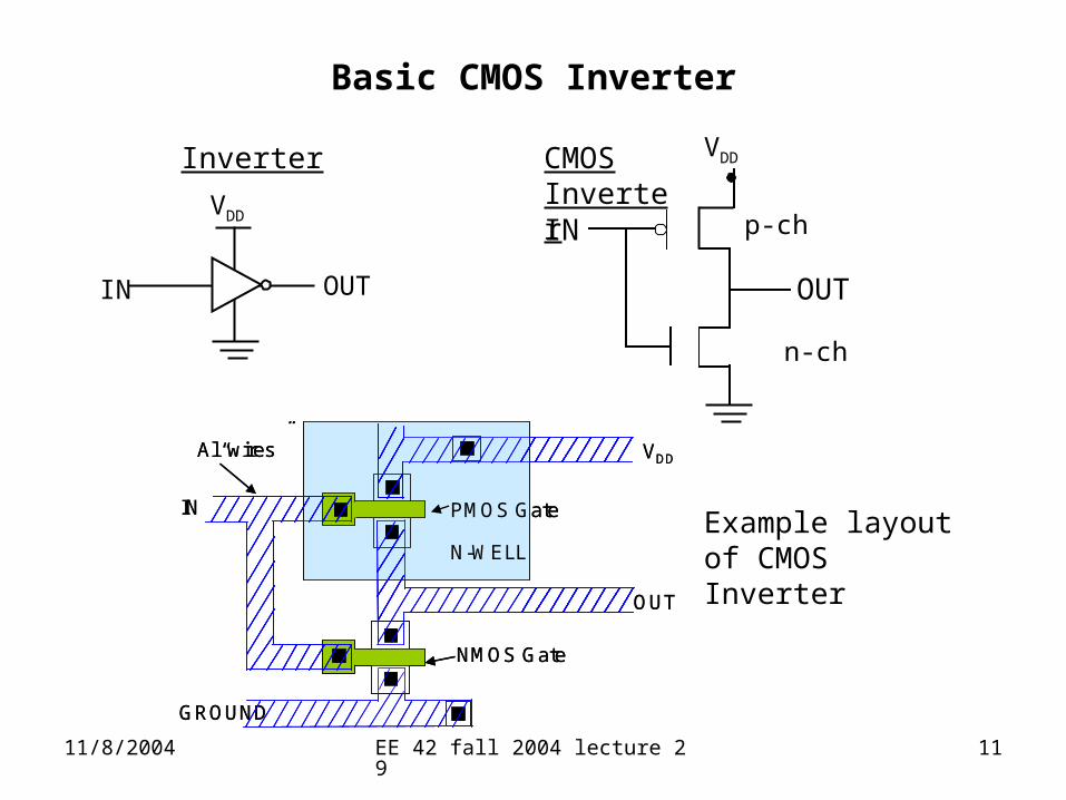
Basic CMOS Inverter
Inverter
IN OUT
VDD p-ch
VDD
OUT
IN
n-ch
CMOS Inverter
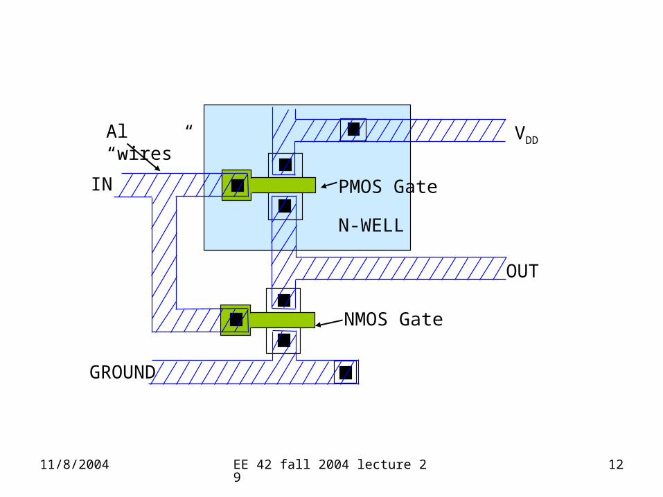
GROUND
IN
OUT
VDD
N-WELL
NMOS Gate
PMOS Gate
Al “wires”
GROUND
IN
OUT
VDD
N-WELL
NMOS Gate
PMOS Gate
Al “wires”
Example layout of CMOS Inverter
11/8/2004 EE 42 fall 2004 lecture 29 12
GROUND
IN
OUT
VDD
N-WELL
NMOS Gate
PMOS Gate
Al “wires”
11/8/2004 EE 42 fall 2004 lecture 29 13
Data Synchronization problem
• Combinatorial logic gates can give incorrect answers prematurely and may take several gate propagation delays produce an answer.
• Clocks (signals as to when to proceed) and latches (which capture and hold the correct outputs) can provide synchronization.
11/8/2004 EE 42 fall 2004 lecture 29 14
Combinatorial vs Sequential logic
• In the digital circuits we have created so far, the output was a function only of the instantaneous inputs. – combinational logic circuits.
• If the action of circuits depends on the history of the inputs, or on past operations, they are– sequential logic circuits.
11/8/2004 EE 42 fall 2004 lecture 29 15
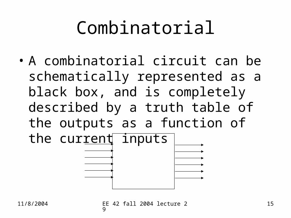
Combinatorial
• A combinatorial circuit can be schematically represented as a black box, and is completely described by a truth table of the outputs as a function of the current inputs
11/8/2004 EE 42 fall 2004 lecture 29 16
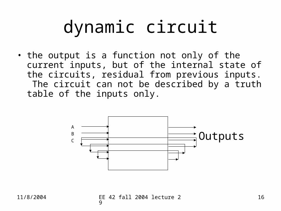
dynamic circuit
• the output is a function not only of the current inputs, but of the internal state of the circuits, residual from previous inputs. The circuit can not be described by a truth table of the inputs only.
A
B
C Outputs
11/8/2004 EE 42 fall 2004 lecture 29 17
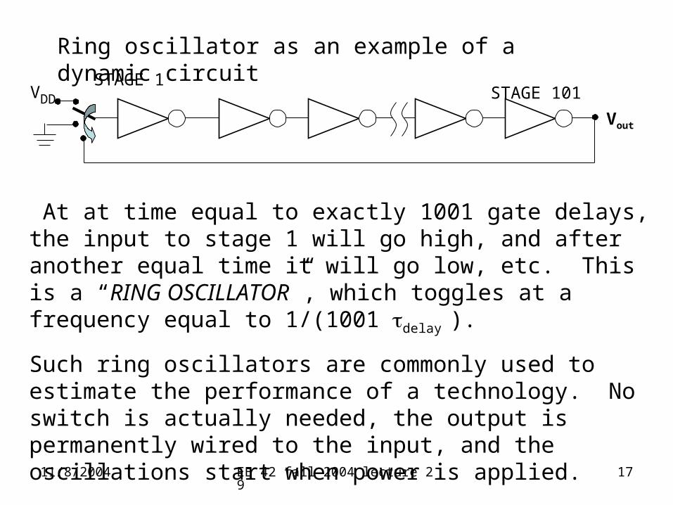
Ring oscillator as an example of a dynamic circuit
Vout
STAGE 1VDD STAGE 101
At at time equal to exactly 1001 gate delays, the input to stage 1 will go high, and after another equal time it will go low, etc. This is a “RING OSCILLATOR”, which toggles at a frequency equal to 1/(1001 delay ).
Such ring oscillators are commonly used to estimate the performance of a technology. No switch is actually needed, the output is permanently wired to the input, and the oscillations start when power is applied.
11/8/2004 EE 42 fall 2004 lecture 29 18
Unpredictability of dynamic circuits
• In the case of the ring oscillator, the output just oscillates forever without regard to its inputs.
• If there are many different paths and possible delays, the output of the circuit can be highly unpredictable or chaotic, because just what may happen at an instant in time can depend on the exact value of all the previous delays.
11/8/2004 EE 42 fall 2004 lecture 29 19
Representing a Discrete Sequence in Continuous Time
• From our viewpoint, time appears to be a continuous variable.
• For a digital sequence, we want discrete values• [x0,!x1, x2, x3, …], not a continuous function
x(t).• The typical way to handle this is to use a clock.• The continuous sequence is “sampled” at
regularly spaced times, when the clock “ticks”.
11/8/2004 EE 42 fall 2004 lecture 29 20
Making time discrete
• The most common answer to this complexity is the same one we used for simplifying circuits before, but this now we make time discrete.
• Rather than letting all of the internal nodes take logical states at arbitrary times, we use latches to prevent the change of state of some nodes until a specific time.
11/8/2004 EE 42 fall 2004 lecture 29 21
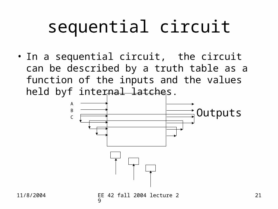
sequential circuit
• In a sequential circuit, the circuit can be described by a truth table as a function of the inputs and the values held byf internal latches.
A
B
C Outputs
11/8/2004 EE 42 fall 2004 lecture 29 22
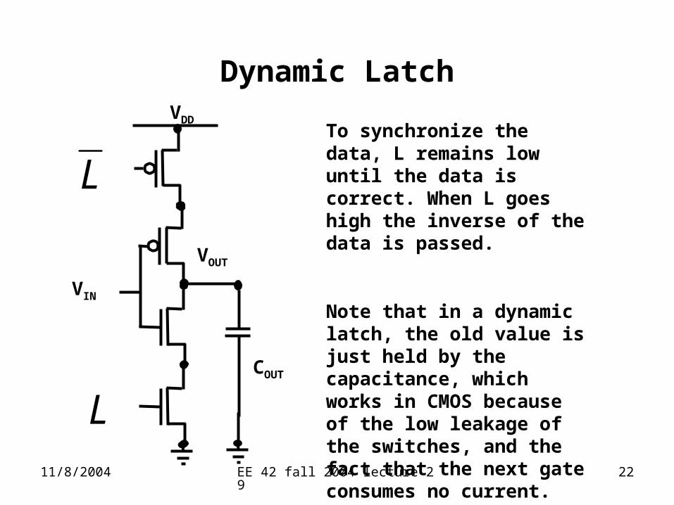
Dynamic Latch
To synchronize the data, L remains low until the data is correct. When L goes high the inverse of the data is passed.
Note that in a dynamic latch, the old value is just held by the capacitance, which works in CMOS because of the low leakage of the switches, and the fact that the next gate consumes no current. When L is low, the voltage at the output is left floating
COUT
VDD
VOUT
VIN
L
L
11/8/2004 EE 42 fall 2004 lecture 29 23
Latches
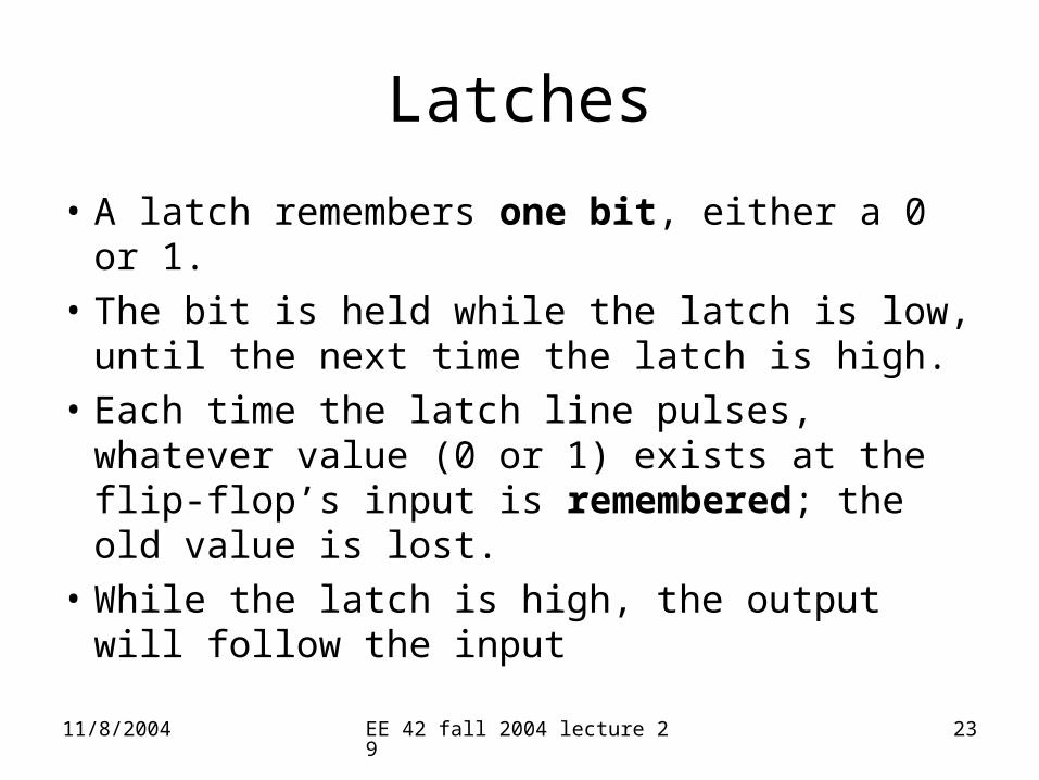
• A latch remembers one bit, either a 0 or 1.
• The bit is held while the latch is low, until the next time the latch is high.
• Each time the latch line pulses, whatever value (0 or 1) exists at the flip-flop’s input is remembered; the old value is lost.
• While the latch is high, the output will follow the input
11/8/2004 EE 42 fall 2004 lecture 29 24
Feedback Can Provide Memory
Q
Q
H
H
L
L
H
H
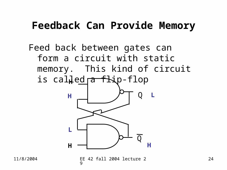
Feed back between gates can form a circuit with static memory. This kind of circuit is called a flip-flop
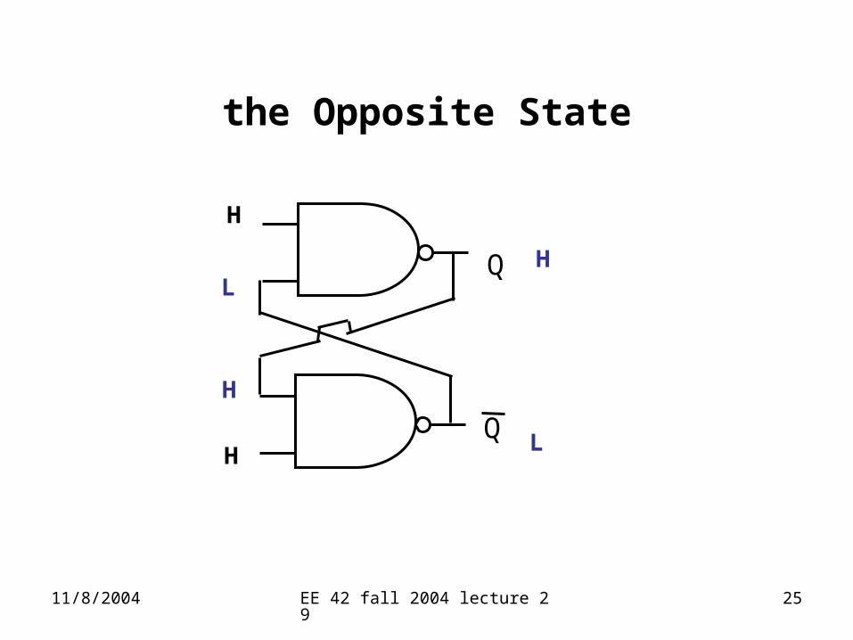
11/8/2004 EE 42 fall 2004 lecture 29 25
the Opposite State
Q
Q
H
H
L
H
H
L
11/8/2004 EE 42 fall 2004 lecture 29 26
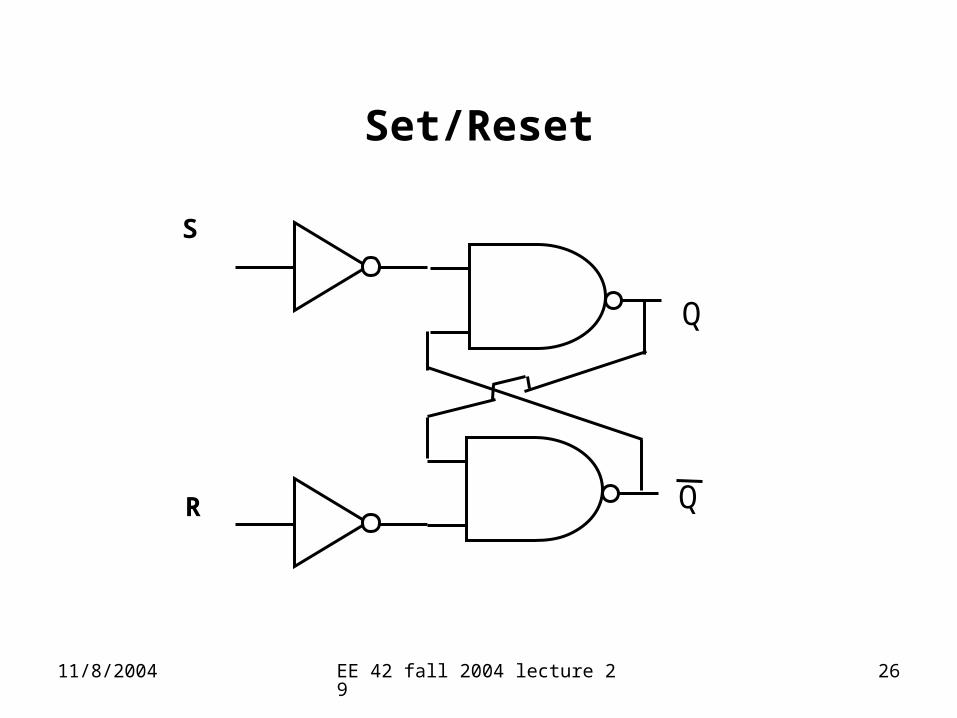
Set/Reset
Q
Q
S
R
11/8/2004 EE 42 fall 2004 lecture 29 27
Set/Reset flip-flop
• This circuit will do the following
1. If S=0 and R=0, Q will not change, but will remember its former value.
2. If S=1 and R=0, then Q=1
3. If S=0 and R=1, then Q=0
4. S=1 and R=1 is an illegal combination
11/8/2004 EE 42 fall 2004 lecture 29 28
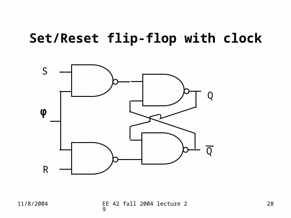
Set/Reset flip-flop with clock
S
R
Q
Q
φ
11/8/2004 EE 42 fall 2004 lecture 29 29
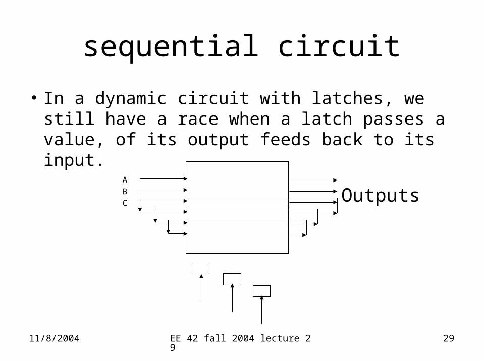
sequential circuit
• In a dynamic circuit with latches, we still have a race when a latch passes a value, of its output feeds back to its input.
A
B
C Outputs
11/8/2004 EE 42 fall 2004 lecture 29 30
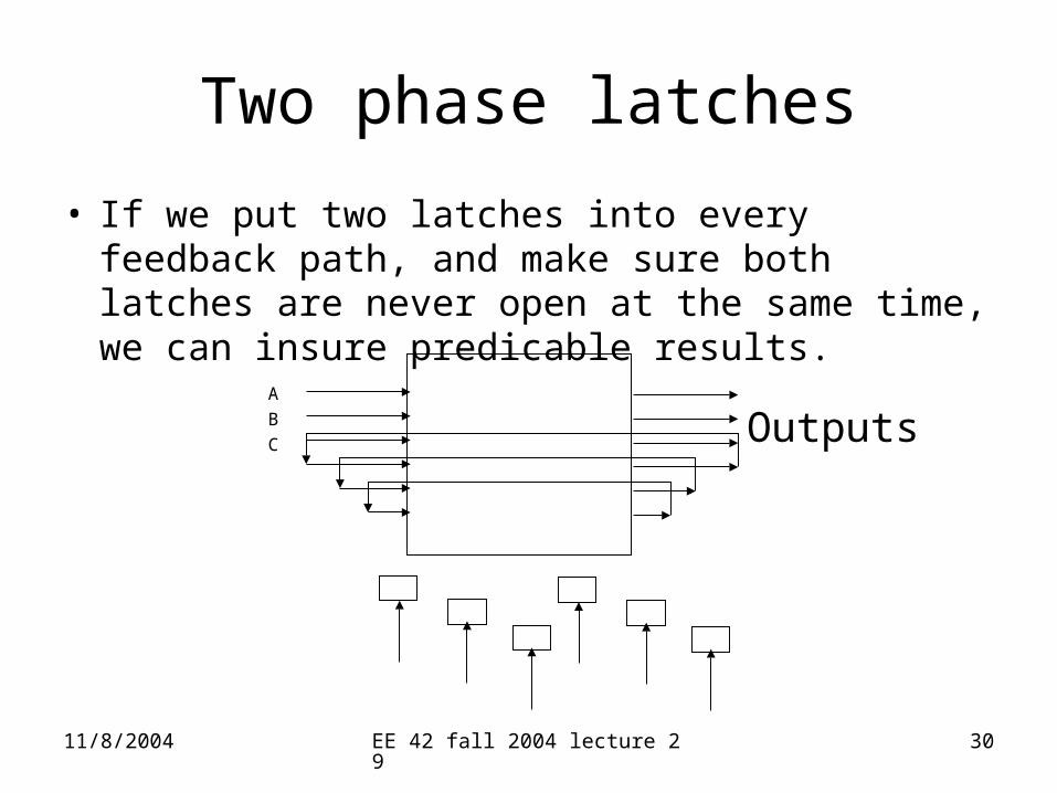
Two phase latches
• If we put two latches into every feedback path, and make sure both latches are never open at the same time, we can insure predicable results.
A
B
C Outputs
11/8/2004 EE 42 fall 2004 lecture 29 31
Asynchronous vs. clocked logic
• One straightforward way of making sure that the behavior is predictable, and does exactly what it was designed to do, is to latch all of the circuits in the block by one signal, which is called a clock.
• If a dynamic circuit is built without a clock, it is called asynchronous logic.
• It is possible to build fast, low power asynchronous circuits, but difficult to make complex systems which behave correctly
11/8/2004 EE 42 fall 2004 lecture 29 32
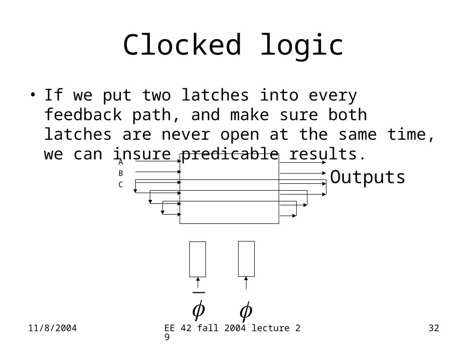
Clocked logic
• If we put two latches into every feedback path, and make sure both latches are never open at the same time, we can insure predicable results.
A
B
C Outputs


![Oil & Gas Catalogue [2019]€¦ · Field programmable for latched, momentary, or safety latched operation. 300 hour continuous transmission with flashing low battery indicator. External](https://img.pdfslide.us/doc/110x75/5e8cb215ef138d34ce613ee9/oil-gas-catalogue-2019-field-programmable-for-latched-momentary-or-safety.jpg)