Embed Size (px)
Citation preview

Lecture 23, Slide 1EECS40, Fall 2004 Prof. White
Lecture #23
OUTLINE• Maximum clock frequency - three figures of merit• Continuously-switched inverters• Ring oscillators
• IC Fabrication Technology
– Doping
– Oxidation
– Thin-film deposition
– Lithography
– Etch
Reading (Rabaey et al.)
• Chapters 5.4 and 2.1-2.2

Lecture 23, Slide 2EECS40, Fall 2004 Prof. White
How to measure inverter performance?
2) The stage delay when the input is a continuous square-wave clock input.
vout1
= v in2
vin1+ -
VDD
MN1MN2
MP3MP4
There are two other measures of performance which we can also consider:
1) We have defined the unit delaytp as the time until Vout1 reaches VDD /2
starting at either 0V (rising) or VDD (falling) . Vin1 is a step function.
3) The delay of a pulse through a multi-stage “ring oscillator”,

Lecture 23, Slide 3EECS40, Fall 2004 Prof. White
Unit gate delay performance measurement
t
Suppose Vin1 goes
from low to high.
The properly designed stage will have similar delay time for rising
input as for falling input. (Design proper ratio of Wp to Wn)
V
vout1
= v in2
vin1+ -
VDD
MN1MN2
MP3MP4 VDD
Because when it reaches this value, the following stage will sense that
its input has switched from high to low. Similarly tpLH is the time for the
output to rise from zero to VDD /2 when the input is falling.
Vout1 goes from VDD to ground.
We defined the inverter delay tpHLas the time until Vout1 reaches VDD /2 .
tp
0.5 VDD
Maximum frequency is just 1/(tpHL + tpLH

Lecture 23, Slide 4EECS40, Fall 2004 Prof. White
Driving Inverters (or gates) with Square-Wave Clock
INV
t
DDVtt
1/f
VDD
In X
Node X loaded by CX
Inverter 1 has output resistance Rp or Rn
Output slowly converges to sawtooth waveform. Let’s find relationship between max and min values vh and vl after many many cycles:
(1) Pull down:XnCΔt/R
hl evv (2) Pull up:
XpCΔt/RDDlDDh )eV(vVv
Example:
can solve simultaneously given t/RC
t1
t
t
t4t3t2t5
etc.
VIN , VX
Lets follow VX for VIN
starting at t=0
Vl
Vh
DDhDDlXnpn 0.73V v,0.27V v CRΔt ,RR

Lecture 23, Slide 5EECS40, Fall 2004 Prof. White
Square-Wave DriveINV
t
DDVtt
1/f
VDD
In YX
Inverter 2 will operate correctly so long as VX passes through vil and vih.We approximate response of devices in inverter 2 as instantaneous (remember the steep transfer curve). Let’s look at VX after a long time.
XV
DDV
ihV
ilV
When VX crosses down through vil, inverter 2 switches, and when it crosses up through vih, it switches back
XV
t1
t
t
t4t3t2t5
etc.

Lecture 23, Slide 6EECS40, Fall 2004 Prof. White
If frequency increases when will inverter fail?
If VX does not pass through Vil or Vih, because frequency is too high.
MAXIMUM CLOCK FREQUENCY fmax : Increase f until inverter 2 fails to toggle because its input does not pass through its threshold(s). In general, Rp Rn, so rise or fall is slower.

Lecture 23, Slide 7EECS40, Fall 2004 Prof. White
Example:
Now consider the square-wave drive case:
Take VDD=2.5V, Vih = 1.5, Vil = 1V , so in this symmetric case:CΔt/R
DDilDDihCΔt/R
ihilpn )eV-V(V vand eVv
Solving either equation with RC = 15pS, t = 6.1pS; fmax2 = 1012/12.2=82GHz
(obviously this result depends on our somewhat arbitrary choice for Vih and Vil )
Take R = 3 K, C = 5 fF, tpHL = tpLH = 0.69 RC = 10pS ;
So fmax1 = 50GHz
XV
DDV
ihV
ilV

Lecture 23, Slide 8EECS40, Fall 2004 Prof. White
Ring Oscillator
As soon as the inverter 1 drives inverter 2’s input past Vil (falling) or Vih (rising), inverter 2 switches and starts driving input node of toward its switch point, etc.
Result: Signal propagates along chain at another kind of maximum clock frequency fmax* (really maximum propagation frequency )
Odd number of stages
Let the average delay per stage be tMIN then the time around loop is N tMIN .
One period is twice around the loop, so , something very
easy to measure. [ If tMIN is 20pSec but N is 1001, the period 1/ fRO is 40 nSec.].O.R
MIN f1
tN2
Nf*f R.O.MAX easy to measure (low frequency)could be 1001
1 2 3 n…4
*2f
1Δt
MAXMIN Now we. define fmax* by ,so
Note: V starts at 0V (rising) or VDD (falling) WHY?
NOTE:
fmax *< fmax2
WHY?

Lecture 23, Slide 9EECS40, Fall 2004 Prof. White
Ring Oscillator
As soon as the switch closes inverter 5 drives inverter 1’s input up (starting at 0 V). When it reaches Vih inverter 1 switches and starts driving input node of inverter two down, starting at VDD. . We note that the transient always starts at 0 or VDD and ends at Vih or Vil , respectively.
This clearly takes longer than the clock-driven chain of inverter transient.
Need to solve same exponential equations as in square-wave drive, but with different limits:
Up: Start at 0, end at Vih.
Down: Start at VDD, end at Vil.
Vih = VDD[1-exp(-tLH/RpC)]
Vil = VDD[exp(-tHL/RnC)]
Solve for tLH and tHL and avg. to get tMIN : tMIN = (tLH + tHL )/2
Odd number of stages
0=0V 1 0 1 1=VDD0
close switch

Lecture 23, Slide 10EECS40, Fall 2004 Prof. White
Ring Oscillator Example
From Vih = VDD[1-exp(-tLH/RpC)] we find tLH = 13.7pS
Similarly from Vil = VDD[exp(-tHL/RnC)] tHL = 13.7pS
Thus the delay through 101 stages, twice is 202 X 13.7 =2.78nS.
The ring oscillator frequency is 109/2.78 = 360 MHz.
Finally, fmax* = 360 X 101 = 36 GHz.
This is of course less than either the 50GHz estimated from unit gate delay or the 82 GHz estimated from square-wave driven max toggle frequency.
101 Stages, same parameters: (RC = 15 pS)
0=0V 1 0 1 1=VDD0
close switch

Lecture 23, Slide 11EECS40, Fall 2004 Prof. White
Integrated Circuit Fabrication
Goal:
Mass fabrication (i.e. simultaneous fabrication) of many “chips”, each a circuit (e.g. a microprocessor or memory chip) containing millions or billions of transistors
Method:
Lay down thin films of semiconductors, metals and insulators and pattern each layer with a process much like printing (lithography).
Materials used in a basic CMOS integrated circuit:• Si substrate – selectively doped in various regions• SiO2 insulator• Polycrystalline silicon – used for the gate electrodes• Metal contacts and wiring

Lecture 23, Slide 12EECS40, Fall 2004 Prof. White
Si Substrates (Wafers)
Crystals are grown from a melt in boules (cylinders) with specified dopant concentrations. They are ground perfectly round and oriented (a “flat” or “notch” is ground along the boule) and then sliced like baloney into wafers. The wafers are then polished.
Typical wafer cost: $50
Sizes: 150 mm, 200 mm, 300 mm diameter
300 mm
“notch” indicatescrystal orientation

Lecture 23, Slide 13EECS40, Fall 2004 Prof. White
Suppose we have a wafer of Si which is p-type and we want to change the surface to n-type. The way in which this is done is by ion implantation. Dopant ions are shot out of an “ion gun” called an ion implanter, into the surface of the wafer.
Typical implant energies are in the range 1-200 keV. After the ion implantation, the wafers are heated to a high temperature (~1000oC). This “annealing” step heals the damage and causes the implanted dopant atoms to move into substitutional lattice sites.
Adding Dopants into Si
Eaton HE3High-Energy Implanter,showing the ion beam hitting theend-station x
SiO2
Si
+ + + +++As+ or P+ or B+ ions
x
SiO2
Si
++ ++ ++ ++++++As+ or P+ or B+ ions

Lecture 23, Slide 14EECS40, Fall 2004 Prof. White
• The implanted depth-profile of dopant atoms is peaked.
• In order to achieve a more uniform dopant profile, high-temperature annealing is used to diffuse the dopants
• Dopants can also be directly introduced into the surface of a wafer by diffusion (rather than by ion implantation) from a dopant-containing ambient or doped solid source
Dopant Diffusion
dopant atomconcentration(logarithmic scale)
as-implanted profile
depth, x

Lecture 23, Slide 15EECS40, Fall 2004 Prof. White
• The favored insulator is pure silicon dioxide (SiO2).
• A SiO2 film can be formed by one of two methods:
1. Oxidation of Si at high temperature in O2 or steam ambient
2. Deposition of a silicon dioxide film
Formation of Insulating Films
ASM A412batchoxidationfurnace
Applied Materials low-pressure chemical-vapor deposition (CVD) chamber

Lecture 23, Slide 16EECS40, Fall 2004 Prof. White
22 SiOOSi
Thermal Oxidation
• Temperature range: 700oC to 1100oC
• Process: O2 or H2O diffuses through
SiO2 and reacts with Si at the interface to form more SiO2
• 1 m of SiO2 formed consumes ~0.5 m of Si
oxidethickness
t
ttime, t
222 22 HSiOOHSi or
“dry” oxidation “wet” oxidation

Lecture 23, Slide 17EECS40, Fall 2004 Prof. White
Thermal oxidation grows SiO2 on Si, but it consumes Si, so the wafer gets thinner. Suppose we grow 1 m of oxide:
Silicon wafer, 100 m thick
Example: Thermal Oxidation of Silicon
99 m thick Si, with 1 m SiO2 all around total thickness = 101 m
99m101m

Lecture 23, Slide 18EECS40, Fall 2004 Prof. White
• The thermal oxidation rate slows with oxide thickness.
Consider a Si wafer with a patterned oxide layer:
Now suppose we grow 0.1 m of SiO2:
SiO2 thickness = 1 m
SiO2 thickness = 1.02 m SiO2 thickness = 0.1 m
Si
Effect of Oxidation Rate Dependence on Thickness
Note the 0.04m step in the Si surface!

Lecture 23, Slide 19EECS40, Fall 2004 Prof. White
Local Oxidation (LOCOS)Window Oxidation
Selective Oxidation Techniques

Lecture 23, Slide 20EECS40, Fall 2004 Prof. White
Chemical Vapor Deposition (CVD) of SiO2
2224 2HSiOOSiH • Temperature range:
350oC to 450oC for silane
• Process: Precursor gases dissociate at
the wafer surface to form SiO2
No Si on the wafer surface is consumed
• Film thickness is controlled by the deposition time
oxidethickness
t
time, t
“LTO”

Lecture 23, Slide 21EECS40, Fall 2004 Prof. White
Polycrystalline silicon (“poly-Si”):
Like SiO2, Si can be deposited by Chemical Vapor Deposition:
• Wafer is heated to ~600oC• Silicon-containing gas (SiH4) is injected into the furnace:
SiH4 = Si + 2H2
Properties:
• sheet resistance (heavily doped, 0.5 m thick) = 20 /
• can withstand high-temperature anneals major advantage
Silicon wafer
Si film made up of crystallites
SiO2
Chemical Vapor Deposition (CVD) of Si

Lecture 23, Slide 22EECS40, Fall 2004 Prof. White
Al
Physical Vapor Deposition (“Sputtering”)
Al AlAr+
Al film
Al target
Ar plasma
waferSometimes the substrateis heated, to ~300oC
Negative Bias ( kV)
Gas pressure: 1 to 10 mTorr
Deposition ratesputtering yield
ion current
I
SI
Ar+
Used to deposit Al films:
Highly energetic argon ions batter the surface of a metal target, knocking atoms loose, which then land on the surface of the wafer

Lecture 23, Slide 23EECS40, Fall 2004 Prof. White
Patterning the Layers
Lithography refers to the process of transferring a pattern to the surface of the wafer
Equipment, materials, and processes needed:• A mask (for each layer to be patterned) with the desired pattern
• A light-sensitive material (called photoresist) covering the wafer so as to receive the pattern
• A light source and method of projecting the image of the mask onto the photoresist (“printer” or “projection stepper” or “projection scanner”)
• A method of “developing” the photoresist, that is selectively removing it from the regions where it was exposed
Planar processing consists of a sequence of additive and subtractive steps with lateral patterning
oxidationdeposition
ion implantation
etching lithography

Lecture 23, Slide 24EECS40, Fall 2004 Prof. White
oxidation
opticalmask
processstep
photoresist coatingphotoresistremoval (ashing)
spin, rinse, dryacid etch
photoresistexposure
The Photo-Lithographic Process
photoresistdevelop

Lecture 23, Slide 25EECS40, Fall 2004 Prof. White
Photoresist Exposure
• A glass mask with a black/clear pattern is used to expose a wafer coated with ~1 m thick photoresist
Areas exposed to UV light are susceptible to chemical removal
Mask
UV light
Lens
Si wafer
Image of mask appears here (3 dark areas, 4 light areas)
Mask image is demagnified by nX
“10X stepper”“4X stepper”“1X stepper”
photoresist

Lecture 23, Slide 26EECS40, Fall 2004 Prof. White
Exposure using “Stepper” Tool
wafer
scribe line
1 2
images
field size increases with technology
generation
Translationalmotion

Lecture 23, Slide 27EECS40, Fall 2004 Prof. White
• Solutions with high pH dissolve the areas which were exposed to UV light; unexposed areas are not dissolved
Developed photoresist
Exposed areas of photoresist
Photoresist Development

Lecture 23, Slide 28EECS40, Fall 2004 Prof. White
• Look at cuts (cross sections) at various planes
Lithography Example
• Mask pattern (on glass plate)
BB
A A
(A-A and B-B)

Lecture 23, Slide 29EECS40, Fall 2004 Prof. White
“A-A” Cross-Section
The resist is exposed in the ranges 0 < x < 2 m & 3 < x < 5 m:
x [m]0 1 2 3 4 5
resist
resist after development
x [m]0 1 2 3 4 5
maskpattern
x [m]0 1 2 3 4 5
The resist will dissolve in high pH solutions wherever it was exposed:
Lecture 23, Slide 30EECS40, Fall 2004 Prof. White
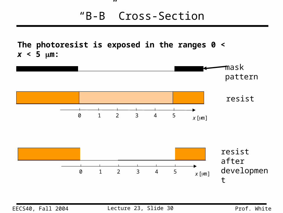
“B-B” Cross-Section
The photoresist is exposed in the ranges 0 < x < 5 m:
x [m]0 1 2 3 4 5
maskpattern
resist
resist after development
x [m]0 1 2 3 4 5

Lecture 23, Slide 31EECS40, Fall 2004 Prof. White
In order to transfer the photoresist pattern to an underlying film, we need a “subtractive” process that removes the film, ideally with minimal change in the pattern and with minimal removal of the underlying material(s)
Selective etch processes (using plasma or aqueous chemistry) have been developed for most IC materials
Jargon for this entire sequence of process steps: “pattern using XX mask”
photoresist
SiO 2
First: pattern photoresist
Si
We have exposed mask pattern, and developed the resist
etch stops on silicon (“selective etchant”)
oxide etchant … photoresist is resistant.
Next: Etch oxide
only resist is attackedLast: strip resist
Pattern Transfer by Etching