Embed Size (px)
Citation preview

1
Lecture 23, Slide 1EE40 Fall 2005 Prof. Neureuther
Diodes: Physical Operation and Models
OUTLINE• Basic Semiconductor Materials• Diode Current and Equation• Some Interesting Circuit Applications
ReadingHambley 10.1-Skim 10.2-10.7
Lecture 23, 10/24/05
Lecture 23, Slide 2EE40 Fall 2005 Prof. Neureuther
Motivation for Last 7 Weeks
Digital Circuits, Logic, D/A, etcWe need a “smart switch,” i.e.,
an electronically controlled switch
We need a “gain element” – for example, to make comparators.
BONUS: MOS is very simple in concept
The device of our dreams exists ! ⇒MOS transistor• a terrific switch
• low power• smart
This week: Basic Semiconductors, Diodes and Diode Uses
Next week: MOS Transistors

2
Lecture 23, Slide 3EE40 Fall 2005 Prof. Neureuther
Game Plan for Last 6 Weeks
1. Learn a little more about semiconductors and pn junction diodes
2. Consider the I vs. V model of diodes and their uses in circuits
3. Learn about MOSFET Operation as a voltage controlled resistor whose current saturates
4. Quiz #2 Wed Nov 2nd: Phasors Analysis, Frequency Response
5. Computer Logic Circuits: Inverter, Gates,
6. Midterm #2 Wed Nov 9th: Phasors Analysis, Frequency Response, Diode Circuits
7. Computer Logic Circuits: Delays, latches and Clocks
8. Circuit Analysis: Transient plus Sinusoidal, 2nd Order Transients
9. Microfabrication and Nano Technology
Topical Flow:
Thus we begin with a very brief review of semiconductors and doping
Lecture 23, Slide 4EE40 Fall 2005 Prof. Neureuther
Conductors, Insulators and Semiconductors
Solids with “free electrons” – that is electrons not directly involved in the inter-atomic bonding- are the familiar metals (Cu, Al, Fe, Au, etc).
Solids with no free electrons are the familiar insulators (glass, quartz crystals, ceramics, etc.)
Silicon is an insulator, but at higher temperatures some of the bonding electrons can get free and make it a little conducting –hence the term “semiconductor”
Pure silicon is a poor conductor (and a poor insulator). It has 4 valence electrons, all of which are needed to bond with nearest neighbors. No free electrons.

3
Lecture 23, Slide 5EE40 Fall 2005 Prof. Neureuther
Electronic Bonds in Silicon
2-D picture of perfect crystal of pure silicon; double line is a Si-Si bond with each line representing an electron
Two electrons in each bond
Si ion(charge+4 q)
Actual structure is 3-dimensional tetrahedral- just like carbon bonding in organic and inorganic materials.
Essentially no free electrons, and no conduction - insulator
Lecture 23, Slide 6EE40 Fall 2005 Prof. Neureuther
How to get conduction in Si?
For the first approach controlled impurities, “dopants”, are added to Si:
or
We must either:1) Chemically modify the Si to produce free carriers (permanent) or
2) Electrically “induce” them by the field effect (switchable)
(Extra electrons produce “free electrons” for conduction.)
Add group V elements (5 bonding electrons vs four for Si), such as phosphorus or arsenic
Deficiency of electrons results in “free holes”
Add group III elements (3 bonding electrons), such as boron

4
Lecture 23, Slide 7EE40 Fall 2005 Prof. Neureuther
Doping Silicon with Donors (n-type)
Donors donate mobile electrons (and thus “n-type” silicon)
Example: add arsenic (As) to the silicon crystal:
Immobile (stuck) positively charged arsenic ion after 5th electron left
As
Mobile electrondonated by As ion
The extra electron with As, “breaks free” and becomes a free electron for conduction
Lecture 23, Slide 8EE40 Fall 2005 Prof. Neureuther
Doping with Acceptors (p-type)
B
Mobile hole con-tributed by B ionand later path
Immobile (stuck) negative boron ion after accepting electron from neighboring bond
Group III element (boron, typically) is added to the crystal
The “hole” which is a missing bonding electron, breaks free from the B acceptor and becomes a roaming positive charge, free to carry current in the semiconductor. It is positively charged.
5
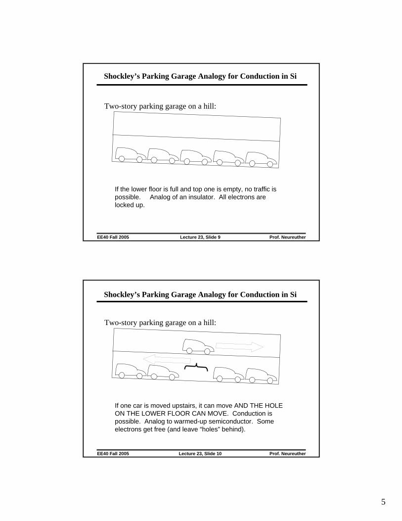
Lecture 23, Slide 9EE40 Fall 2005 Prof. Neureuther
If the lower floor is full and top one is empty, no traffic is possible. Analog of an insulator. All electrons are locked up.
Shockley’s Parking Garage Analogy for Conduction in Si
Two-story parking garage on a hill:
Lecture 23, Slide 10EE40 Fall 2005 Prof. Neureuther
If one car is moved upstairs, it can move AND THE HOLE ON THE LOWER FLOOR CAN MOVE. Conduction is possible. Analog to warmed-up semiconductor. Some electrons get free (and leave “holes” behind).
Shockley’s Parking Garage Analogy for Conduction in Si
Two-story parking garage on a hill:

6
Lecture 23, Slide 11EE40 Fall 2005 Prof. Neureuther
If an extra car is “donated” to the upper floor, it can move. Conduction is possible. Analog to N-type semiconductor.(An electron donor is added to the crystal, creating free electrons).
Shockley’s Parking Garage Analogy for Conduction in Si
Two-story parking garage on a hill:
Lecture 23, Slide 12EE40 Fall 2005 Prof. Neureuther
If a car is removed from the lower floor, it leaves a HOLE which can move. Conduction is possible. Analog to P-type semiconductor. (Acceptors are added to the crystal, “consuming” bonding electrons,creating free holes).
Shockley’s Parking Garage Analogy for Conduction in Si
Two-story parking garage on a hill:

7
Lecture 23, Slide 13EE40 Fall 2005 Prof. Neureuther
Summary of n- and p-type silicon
Pure silicon is an insulator. At high temperatures it conducts weakly.
If we add an impurity with extra electrons (e.g. arsenic, phosphorus) these extra electrons are set free and we have a pretty good conductor (n-type silicon).
If we add an impurity with a deficit of electrons (e.g. boron) then bonding electrons are missing (holes), and the resulting holes can move around … again a pretty good conductor (p-type silicon)
Now what is really interesting is when we join n-type and p-type silicon, that is make a pn junction. It has interesting electrical properties.
Lecture 23, Slide 14EE40 Fall 2005 Prof. Neureuther
Junctions of n- and p-type Regions
A silicon chip may have 108 to 109 p-n junctions today.
p-n junctions form the essential basis of all semiconductor devices.
How do they behave*? What happens to the electrons and holes?What is the electrical circuit model for such junctions?
n and p regions are brought into contact :
n p
aluminum aluminum
wire
?
*Note that the textbook has a very good explanation.
8
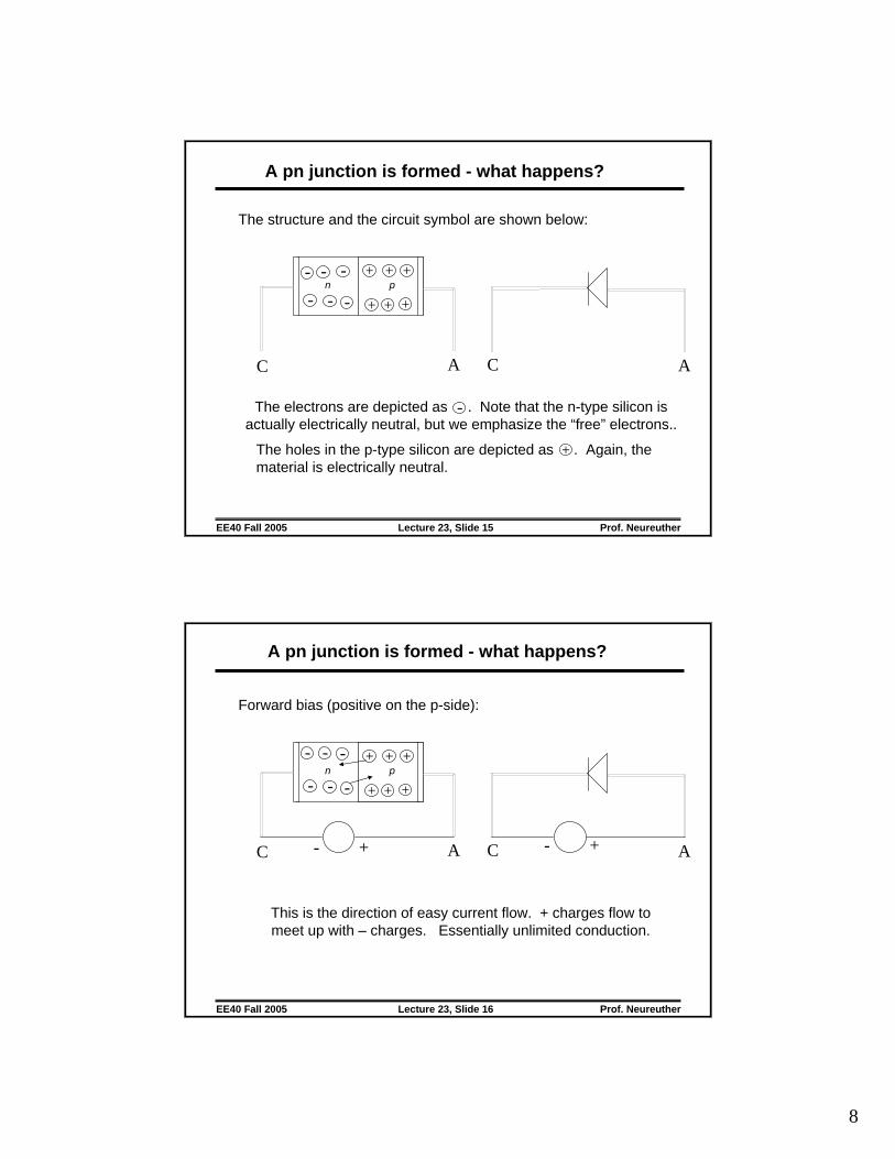
Lecture 23, Slide 15EE40 Fall 2005 Prof. Neureuther
A pn junction is formed - what happens?
The structure and the circuit symbol are shown below:
The holes in the p-type silicon are depicted as . Again, the material is electrically neutral.
+
The electrons are depicted as . Note that the n-type silicon is actually electrically neutral, but we emphasize the “free” electrons..
-
AC
n pp
--- + + +
+ + +
AC
- - -
Lecture 23, Slide 16EE40 Fall 2005 Prof. Neureuther
A pn junction is formed - what happens?
Forward bias (positive on the p-side):
n pp- - -
--- + + +
+ + +
AC AC- + - +
This is the direction of easy current flow. + charges flow to meet up with – charges. Essentially unlimited conduction.
9
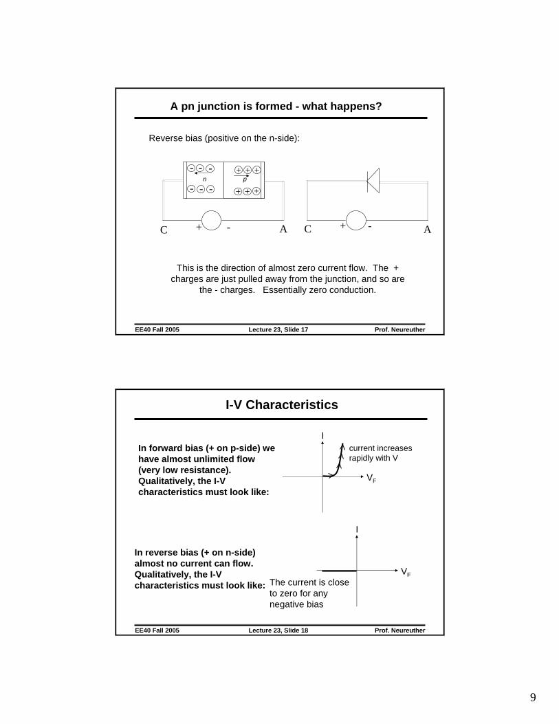
Lecture 23, Slide 17EE40 Fall 2005 Prof. Neureuther
A pn junction is formed - what happens?
Reverse bias (positive on the n-side):
n pp- - -
--- + + +
+ + +
AC AC+ - + -
This is the direction of almost zero current flow. The + charges are just pulled away from the junction, and so are
the - charges. Essentially zero conduction.
Lecture 23, Slide 18EE40 Fall 2005 Prof. Neureuther
I-V Characteristics
In forward bias (+ on p-side) we have almost unlimited flow (very low resistance). Qualitatively, the I-V characteristics must look like:
VF
Icurrent increases rapidly with V
VF
I
The current is close to zero for any negative bias
In reverse bias (+ on n-side) almost no current can flow. Qualitatively, the I-V characteristics must look like:

10
Lecture 23, Slide 19EE40 Fall 2005 Prof. Neureuther
Diode Physical Behavior and Equation
Ntype
Ptype
Schematic Device
+−V
I
ISymbol
+−V
Qualitative I-V characteristics:I
V
V positive, easy conduction
V negative, no conduction
Quantitative I-V characteristics:
)1e(II kTqV0 −=
In which kT/q is 0.026V and IO is a constant depending on diode area. Typical values: 10-12 to 10-16 A. Interestingly, the graph of this equation looks just like the figure to the left.
A non-ideality factor n times kT/q is often included.
Lecture 23, Slide 20EE40 Fall 2005 Prof. Neureuther
The pn Junction I vs. V Equation
In EECS 105, 130, and other courses you will learn why the I vs. V relationship for PN junctions is of the form
)1e(II kTqV0 −=
where I0 is a constant proportional to junction area and depending on doping in P and N regions, k is Boltzman constant, and T is absolute temperature.
a typical value for I0 is
,106.1hargec electronicq 19−×==
,Kat300 0.026VqKT °= A1010 1512 −− −
We note that in forward bias, I increases exponentially and is in the µA-mA range for voltages typically in the range of 0.6-0.8V. In reverse bias, the current is essentially zero.
I-V characteristic of PN junctions

11
Lecture 23, Slide 21EE40 Fall 2005 Prof. Neureuther
Diode Ideal (Perfect Rectifier) Model
The equation
is graphed below for
1)kTqVexp(II 0 −=
A10I 150
−=
The characteristic is described as a “rectifier” – that is, a device that permits current to pass in only one direction. (The hydraulic analog is a “check value”.) Hence the symbol:
+− V
I
Simple “Perfect Rectifier” Model
If we can ignore the small forward-bias voltage drop of a diode, a simple effective model is the “perfect rectifier,” whose I-V characteristic is given below:
V
I
Reverse bias0Vany ,0I <≅
Forward bias0Iany ,0V >≅
A perfect rectifier
0
2
4
6
8
10
-5 0 5 10
Current in mA
Forward Voltage in V
Lecture 23, Slide 22EE40 Fall 2005 Prof. Neureuther
Diode Large-Signal Model (0.7 V Drop)
Improved “Large-Signal Diode” Model:If we choose not to ignore the small forward-bias voltage drop of a diode, it is a very good approximation to regard the voltage drop in forward bias as a constant, about 0.7V. the “Large signal model” results.
Reverse bias0Vany ,0I <≅
Forward bias0Iany ,0.7V >≅
0100200300400
-5 -3 -1 1forward bias (V)
Cur
rent
(m
icro
amp)
+− V
I
The Large-Signal Diode Model
- 0.7+
V
I
0.7

12
Lecture 23, Slide 23EE40 Fall 2005 Prof. Neureuther
Cool Things That a Diode Can Do: Rectifier
VS(t)
t
+
−
VR(t)+−VS(t)
VR(t)
“rectified” version of input waveform
t
Assume the ideal (perfect rectifier)
model.
Lecture 23, Slide 24EE40 Fall 2005 Prof. Neureuther
Cool Things That a Diode Can Do: Peak Detector
+
−
VC(t)Vi(t)+
−
C
Vi(t)
Vi
t
VC(t) VC
+−
Assume the ideal (perfect rectifier) model.
Key Point: The capacitor charges due to one way current behavior of the diode.