Embed Size (px)
Citation preview

2.996/6.971 Biomedical Devices Design Laboratory
Lecture 2: Fundamentals and PCB Layout
Instructor: Hong MaSept. 12, 2007
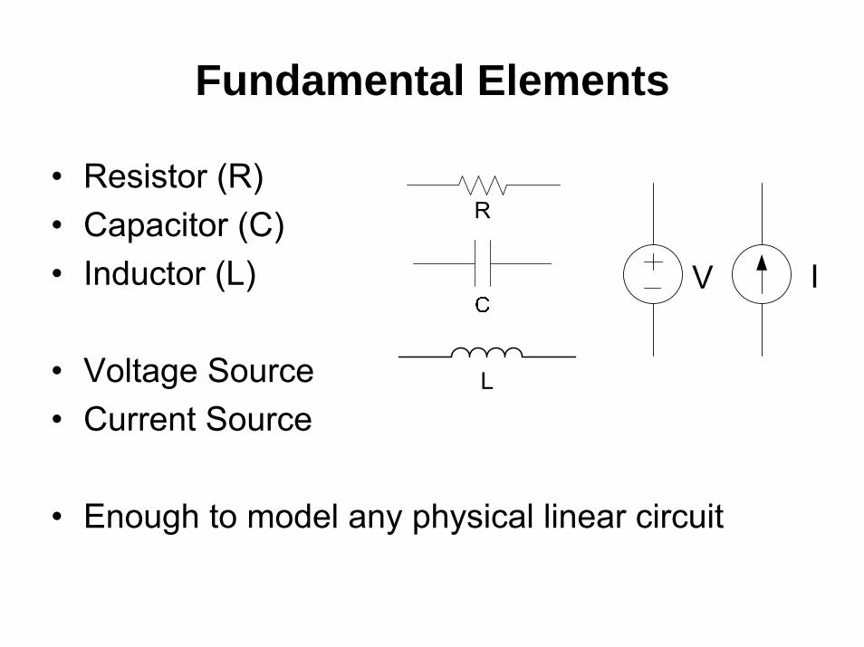
Fundamental Elements
• Resistor (R)• Capacitor (C)• Inductor (L)
• Voltage Source• Current Source
• Enough to model any physical linear circuit

Fundamental Relationships
• Ohm’s law: R = V / I• KVL, KCL – Conservation laws• Impedance:
– Treat capacitors and inductors as resistors
• Fundamental question: – Given an arbitrary circuit, what happens when you
hook up another circuit up to it?
1CZ
j Cω= LZ j Lω=

Thevenin-Norton Equivalents
• Represent an arbitrary circuit using a source and a source impedance
• Thevenin and Norton representation is equivalent
• Result: Reduce all circuits into one fundamental circuit

Source and Load
• Optimize for Voltage: ZLOAD >> ZSOURCE
• Optimize for Current: ZLOAD << ZSOURCE
• Optimize for Power: ZLOAD = ZSOURCE
• Purpose of amplifier / active circuit:– impedance transform
SourcesPower supplySignal GeneratorSensorAmplifier output
LoadsActuatorMeasurement deviceAmplifier input

Simple Filters
• RC Low pass• RC high pass• Bandpass• Bandstop (notch)
Simple Cascaded Filters
• What if 2 stages are needed?
Practical Introduction to Passive Components

Resistors
• Range: 1Ω to 22MΩ• Carbon composite (axial)
– 5% accuracy typical• Wirewound
– 1% accuracy typical• Thick film (Screen printed / electroplated)
– Accuracies down to 1%• Thin film (Vacuum deposited)
– Accuracies down to 0.1%• Temperature coefficient: 20-200 ppm / °C
Images removed due to copyright restrictions.Photo examples of resistors.
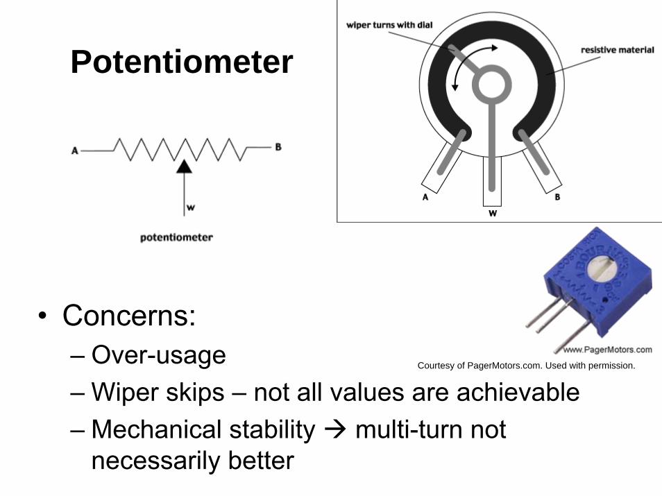
Potentiometer
• Concerns:– Over-usage– Wiper skips – not all values are achievable– Mechanical stability multi-turn not
necessarily better
Courtesy of PagerMotors.com. Used with permission.

Practical Capacitor Considerations
• Accuracy: ±10% typical
• Effective series capacitance
• Dielectric soakage (dielectric absorption)
• Temperature dependence
C ESR

Ceramic Capacitors
• Most common type• 1pF to 1µF• Accuracy
– Through-Hole ±20%– SMT ±10%
• Low ESR, loss tangent ≈ 0.002• Temperature coefficient
– Z5U, X7R, C0G (NP0)• Cost = ~$0.01 in quantity
Images removed due to copyright restrictions.Photo examples of ceramic capacitors.

Aluminum Electrolytic Capacitors• Primary use: power supply bypassing• Range: 1µF – 1F Typical: 100µF• Cost: ~$0.10 depending on size
• Polar, designated by the negative terminal• Will blow up if reverse biased• Nonpolar versions available
• Very inaccurate • Typical tolerance: +80%, -20%• Limited lifetime• High ESR, loss tangent = R/Xc ≈ 0.2
Images removed due to copyright restrictions.Photo examples of aluminum electrolytic capacitors.

Tantalum Electrolytics
• Similar to aluminum electrolytics, but better energy density
• More expensive than aluminum electrolytics• Range: 0.1µF to 1000µF• Polarity designated by the positive terminal
Images removed due to copyright restrictions.Photo examples of tantalum electrolytics.

Double Layer Capacitors
• Extremely high capacitance• Range 0.1F – 1000F• Low voltage rating• Used for energy storage
Images removed due to copyright restrictions.Photo examples of double layer capacitors.

Specialty Capacitors: Polypropylene• Improved performance:
– Accuracy– ESR at high frequencies– Low dielectric soakage– Temperature stability– Higher breakdown voltage
• Tradeoffs– Larger size– Smaller range of values– Higher cost: ~$0.10
Image removed due to copyright restrictions.Photo of polypropylene capacitor.

Power Supply Bypassing• Ideal sources do not exist!• Source impedance increases with
frequency• Ceramic capacitor on each IC component• Electrolytic on both sides of the power
supply

Practical Inductors
• Inaccurate (at best ±10%)• Expensive• Parasitics
– All inductors self resonate• Avoid whenever possible
Images removed due to copyright restrictions.Photo examples of practical inductors.

Where to find information / parts
• Manufacturer’s website: datasheet & samples
• Distributors:– Digikey– Mouser– Newark
• Meta search engine: www.findchips.com
PCB Layers
• Substrate– FR-4 standard; Specialty: G-10, polyimide (Kapton), ceramic– Standard thicknesses: 0.062”, 0.031”
• Copper– 2, 4, up to 12 layers– Minimum trace/spacing 6 mil, smaller is possible– Thickness: 1 oz copper = 500 µΩ per square– Exposed copper tin’ed with solder– Interlayer connection by vias; Blind and buried vias = $$$
• Soldermask – very important Hydrophobic to solder• Silkscreen
Image removed due to copyright restrictions.
PCB Layout Error Sources
• Capacitive interference• Inductive interference• Electromagnetic interference
• Need a ground plane… but why?!?
Image removed due to copyright restrictions.

Capacitive Interference• Cause: capacitance between nearby traces• When to watch out for it:
– High impedance circuit nodes– High-voltage excitation signals– High frequency signals
• How to avoid it:– Lower the circuit impedance– Use groundplanes and shielding to isolate signal lines– Boot-strap to reduce capacitance to ground– Separate analog and digital ground planes

Inductive Interference
• Cause: mutual inductance between traces• When to watch out for it:
– Large AC current– Transient switching– Long traces– Loops
How to Avoid Inductive Interference• Keep traces short• Make traces perpendicular• Use star power / ground routing• Reduce loop area• Careful use of ground planes• Watch out for return lines
Image removed due to copyright restrictions.See Figure 12 here: http://www.analog.com/library/analogdialogue/archives/41-06/ground_bounce.html
Electromagnetic Interference (EMI)• Cause:
– long traces/wires acting as an antenna• When to watch out for it:
– Length > 1/20 wavelength• Source of interference
– Wireless communication (900MHz, 2.4GHz, 5GHz)– FM radio– Microwave oven– Lightning, solar flares, cosmic rays– High speed processors
• Real products must pass FCC and CE testing

Ferrite Bead• A lossy inductor• Resistor at high frequencies
Example photos removed due to copyright restrictions.
Where to put the ground planes?
• Ground planes outside, signals inside:– Essentially eliminate capacitive interference
• Ground planes inside, signal outside:– Ground plane with frewer interruptions
Image removed due to copyright restrictions.

Project Teams