Embed Size (px)
Citation preview

Department of EECS University of California, Berkeley
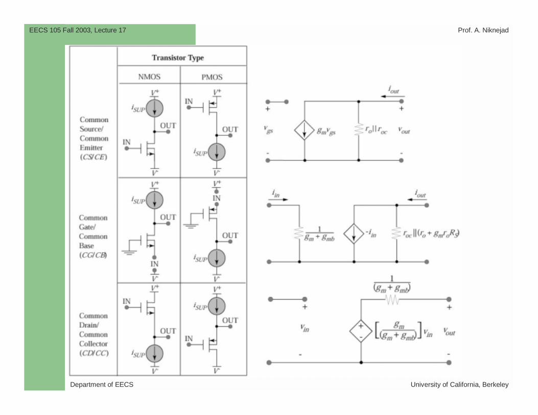
EECS 105 Fall 2003, Lecture 17
Lecture 17:
Common Source/Gate/Drain Amplifiers
Prof. Niknejad

Department of EECS University of California, Berkeley
EECS 105 Fall 2003, Lecture 17 Prof. A. Niknejad
Lecture Outline
MOS Common Source Amp
Current Source Active Load
Common Gate Amp
Common Drain Amp

Department of EECS University of California, Berkeley
EECS 105 Fall 2003, Lecture 17 Prof. A. Niknejad
Common-Source Amplifier
Isolate DC level
Department of EECS University of California, Berkeley
EECS 105 Fall 2003, Lecture 17 Prof. A. Niknejad
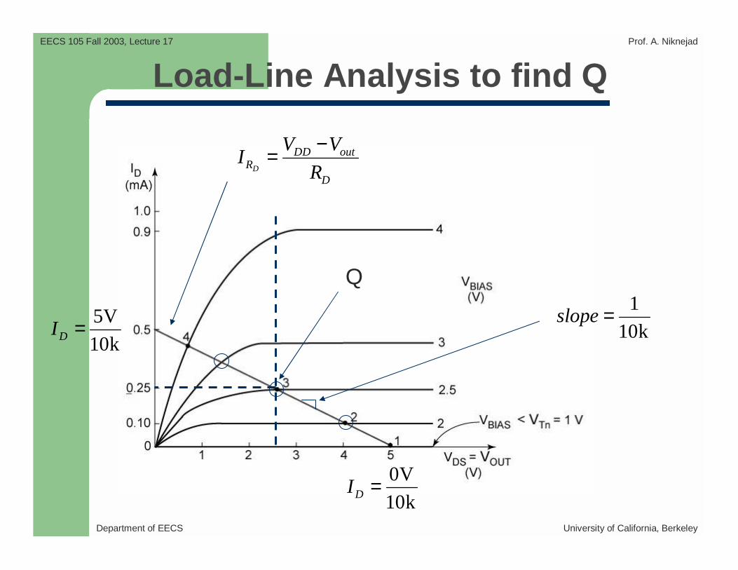
Load-Line Analysis to find Q
Q
D
DD outR
D
V VI
R
−=
1
10kslope =
0V
10kDI =
5V
10kDI =
Department of EECS University of California, Berkeley
EECS 105 Fall 2003, Lecture 17 Prof. A. Niknejad
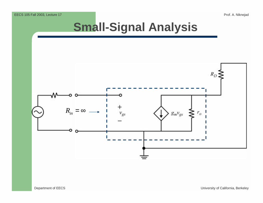
Small-Signal Analysis
inR = ∞
Department of EECS University of California, Berkeley
EECS 105 Fall 2003, Lecture 17 Prof. A. Niknejad
sv
sR
inRoutR LRm inG v
inv
+
−
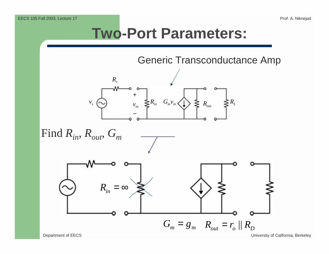
Two-Port Parameters:
Find Rin, Rout, Gm
inR = ∞
m mG g= ||out o DR r R=
Generic Transconductance Amp
Department of EECS University of California, Berkeley
EECS 105 Fall 2003, Lecture 17 Prof. A. Niknejad
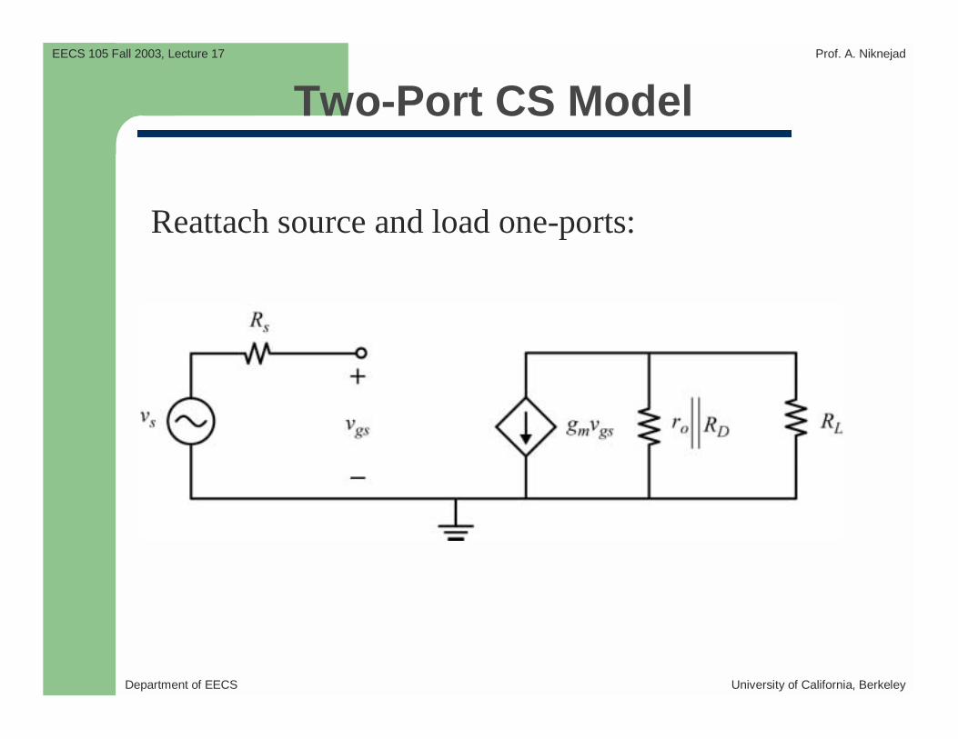
Two-Port CS Model
Reattach source and load one-ports:
Department of EECS University of California, Berkeley
EECS 105 Fall 2003, Lecture 17 Prof. A. Niknejad
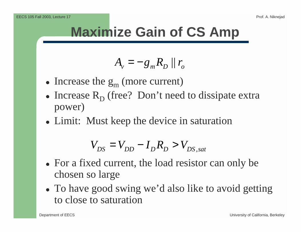
Maximize Gain of CS Amp
Increase the gm (more current) Increase RD (free? Don’t need to dissipate extra
power) Limit: Must keep the device in saturation
For a fixed current, the load resistor can only be chosen so large
To have good swing we’d also like to avoid getting to close to saturation
||v m D oA g R r= −
,DS DD D D DS satV V I R V= − >

Department of EECS University of California, Berkeley
EECS 105 Fall 2003, Lecture 17 Prof. A. Niknejad
Current Source Supply
Solution: Use a current source!
Current independent of voltage for ideal source
Department of EECS University of California, Berkeley
EECS 105 Fall 2003, Lecture 17 Prof. A. Niknejad
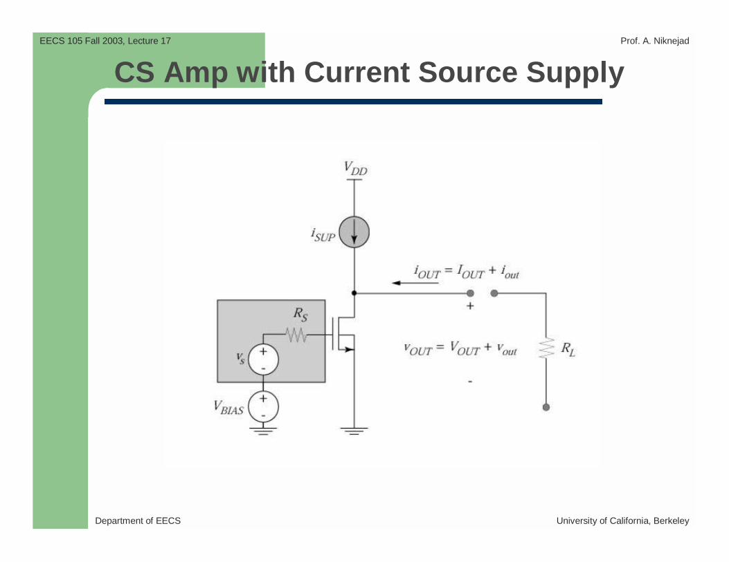
CS Amp with Current Source Supply

Department of EECS University of California, Berkeley
EECS 105 Fall 2003, Lecture 17 Prof. A. Niknejad
Load Line for DC Biasing
Both the I-source and the transistor are idealized for DC bias analysis
Department of EECS University of California, Berkeley
EECS 105 Fall 2003, Lecture 17 Prof. A. Niknejad
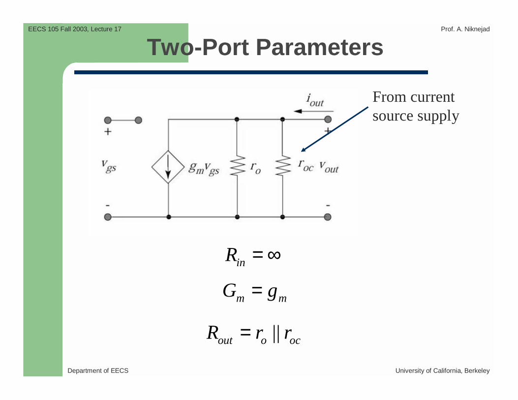
Two-Port Parameters
From currentsource supply
inR = ∞
||out o ocR r r=
m mG g=

Department of EECS University of California, Berkeley
EECS 105 Fall 2003, Lecture 17 Prof. A. Niknejad
P-Channel CS Amplifier
DC bias: VSG = VDD – VBIAS sets drain current –IDp = ISUP
Department of EECS University of California, Berkeley
EECS 105 Fall 2003, Lecture 17 Prof. A. Niknejad
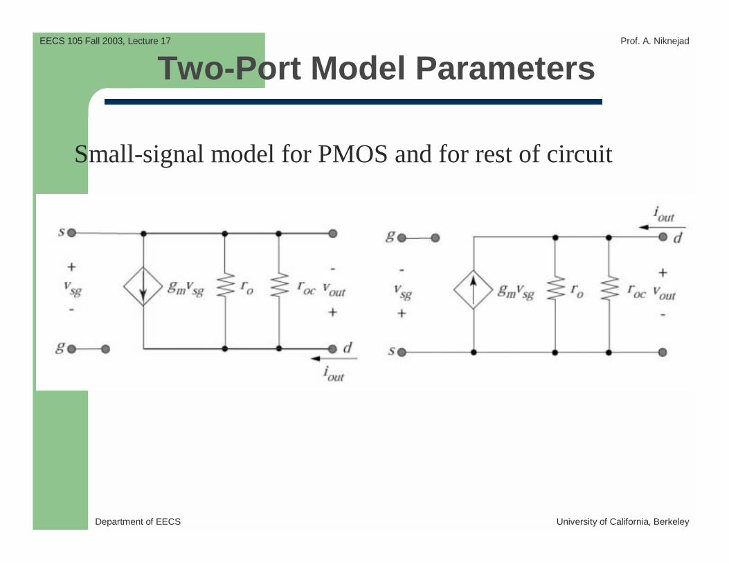
Two-Port Model Parameters
Small-signal model for PMOS and for rest of circuit

Department of EECS University of California, Berkeley
EECS 105 Fall 2003, Lecture 17 Prof. A. Niknejad
Common Gate Amplifier
DC bias:
SUP BIAS DSI I I= =
Department of EECS University of California, Berkeley
EECS 105 Fall 2003, Lecture 17 Prof. A. Niknejad
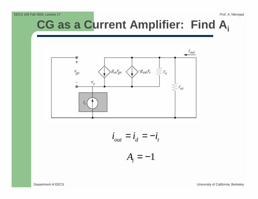
CG as a Current Amplifier: Find Ai
out d ti i i= = −
1iA = −
Department of EECS University of California, Berkeley
EECS 105 Fall 2003, Lecture 17 Prof. A. Niknejad
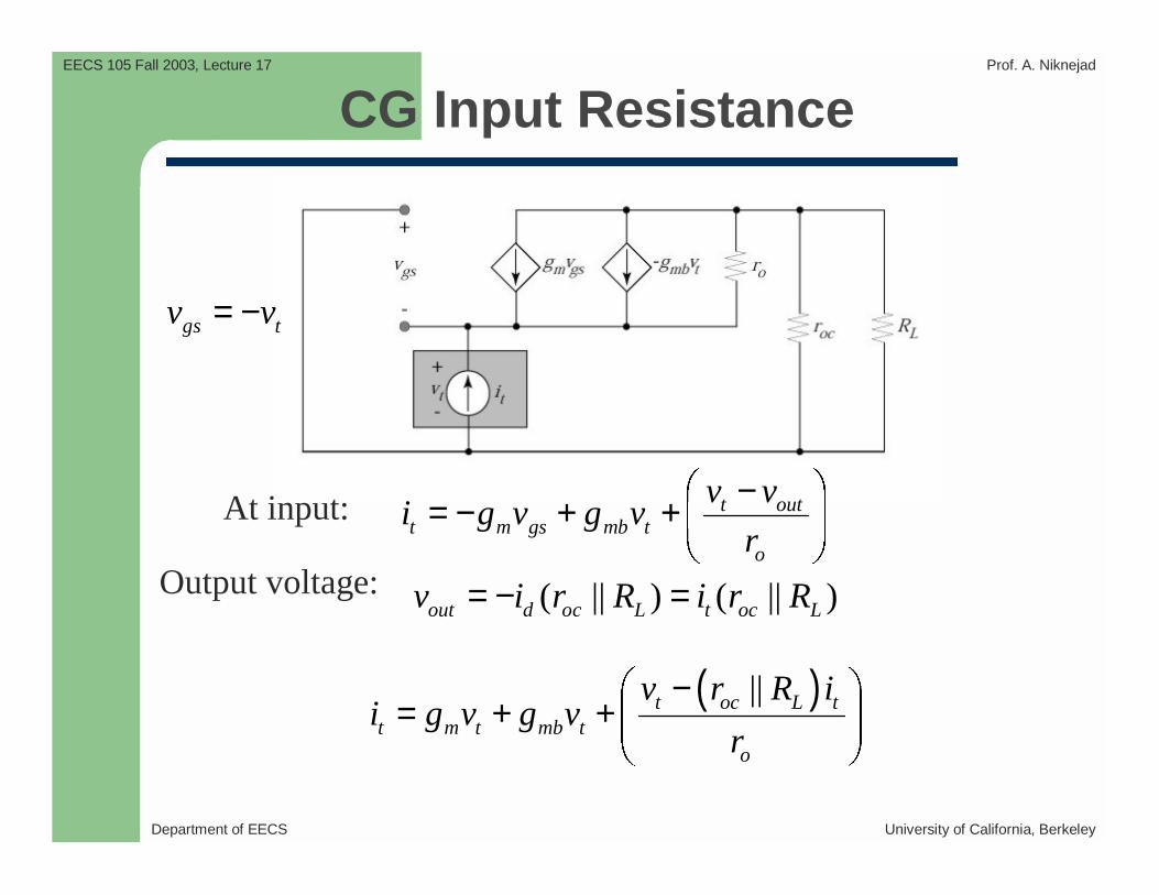
CG Input Resistance
At input:
Output voltage:
t outt m gs mb t
o
v vi g v g v
r
−= − + +
( || ) ( || )out d oc L t oc Lv i r R i r R= − =
gs tv v= −
( )||t oc L tt m t mb t
o
v r R ii g v g v
r
−= + +
Department of EECS University of California, Berkeley
EECS 105 Fall 2003, Lecture 17 Prof. A. Niknejad
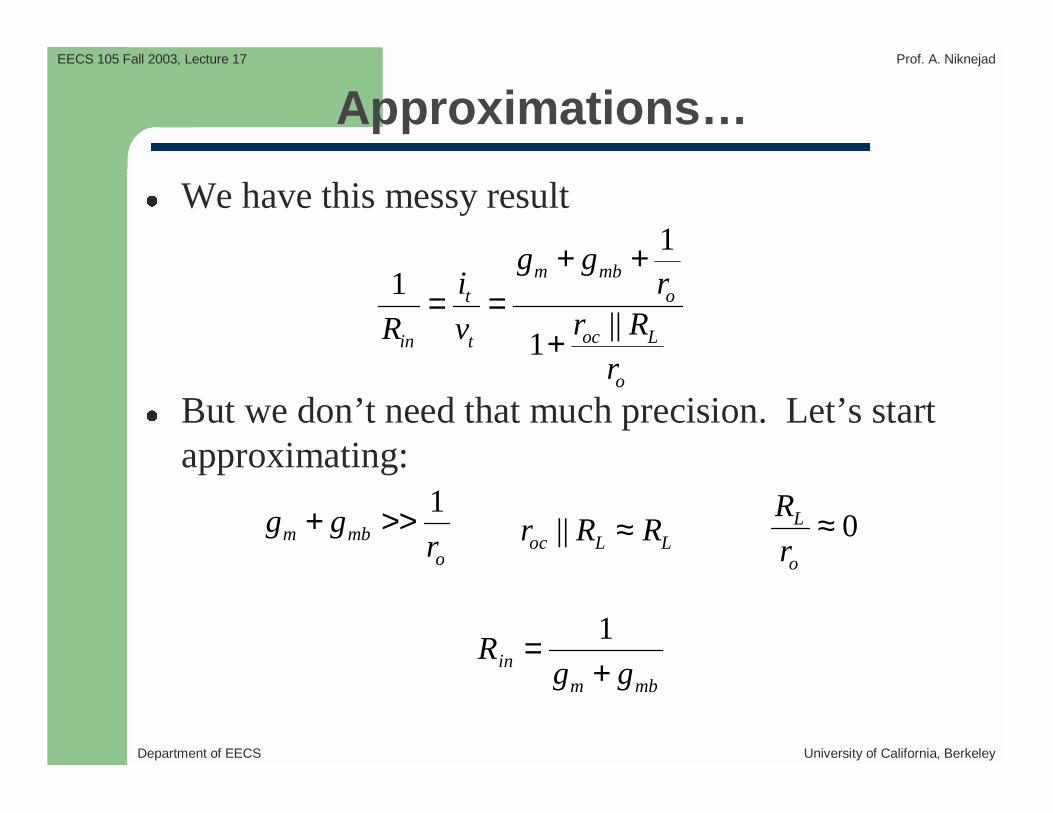
Approximations…
We have this messy result
But we don’t need that much precision. Let’s start approximating:
11
||1
m mbt o
oc Lin t
o
g gi r
r RR vr
+ += =
+
1m mb
o
g gr
+ >> ||oc L Lr R R≈ 0L
o
R
r≈
1in
m mb
Rg g
=+

Department of EECS University of California, Berkeley
EECS 105 Fall 2003, Lecture 17 Prof. A. Niknejad
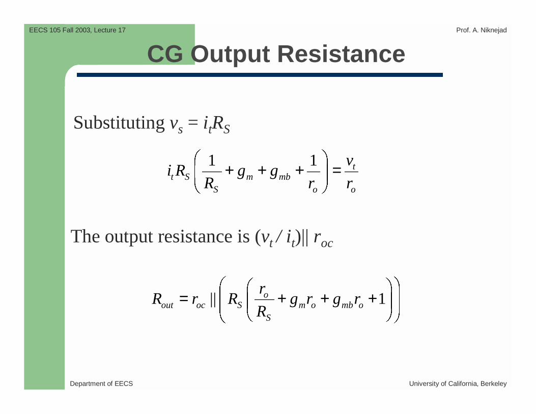
CG Output Resistance
( ) 0s s tm gs mb s
S o
v v vg v g v
R r
−− − − + =
1 1 ts m mb
S o o
vv g g
R r r
+ + + =
Department of EECS University of California, Berkeley
EECS 105 Fall 2003, Lecture 17 Prof. A. Niknejad
CG Output Resistance
Substituting vs = itRS
1 1 tt S m mb
S o o
vi R g g
R r r
+ + + =
The output resistance is (vt / it)|| roc
|| 1oout oc S m o mb o
S
rR r R g r g r
R
= + + +
Department of EECS University of California, Berkeley
EECS 105 Fall 2003, Lecture 17 Prof. A. Niknejad
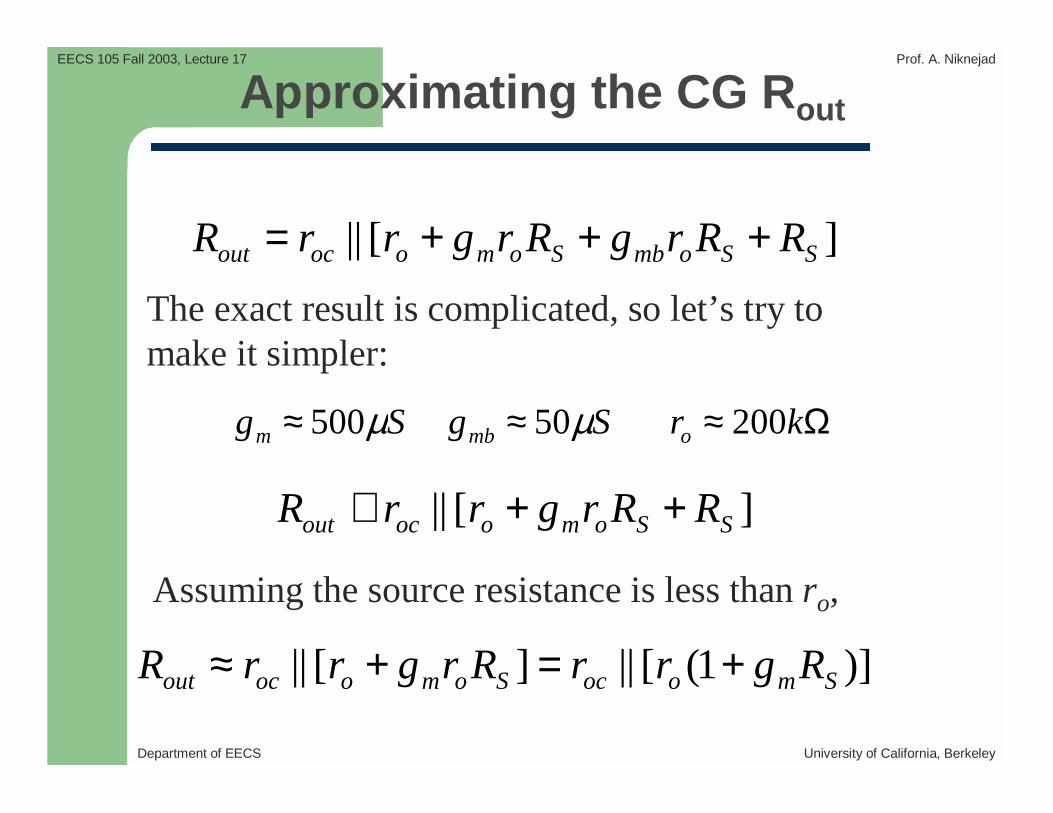
Approximating the CG Rout
The exact result is complicated, so let’s try tomake it simpler:
Sgm µ500≈ Sgmb µ50≈ Ω≈ kro 200
][|| SSombSomoocout RRrgRrgrrR +++=
][|| SSomoocout RRrgrrR ++≅
Assuming the source resistance is less than ro,
)]1([||][|| SmoocSomoocout RgrrRrgrrR +=+≈
Department of EECS University of California, Berkeley
EECS 105 Fall 2003, Lecture 17 Prof. A. Niknejad
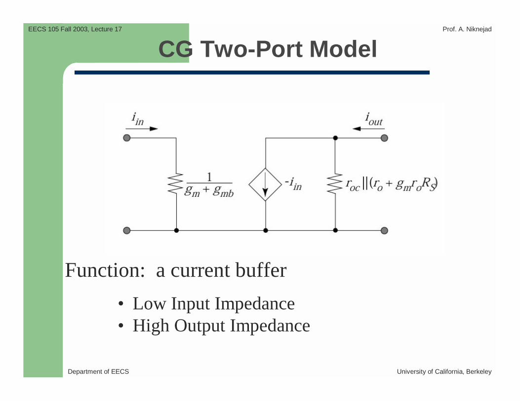
CG Two-Port Model
Function: a current buffer
• Low Input Impedance• High Output Impedance
Department of EECS University of California, Berkeley
EECS 105 Fall 2003, Lecture 17 Prof. A. Niknejad
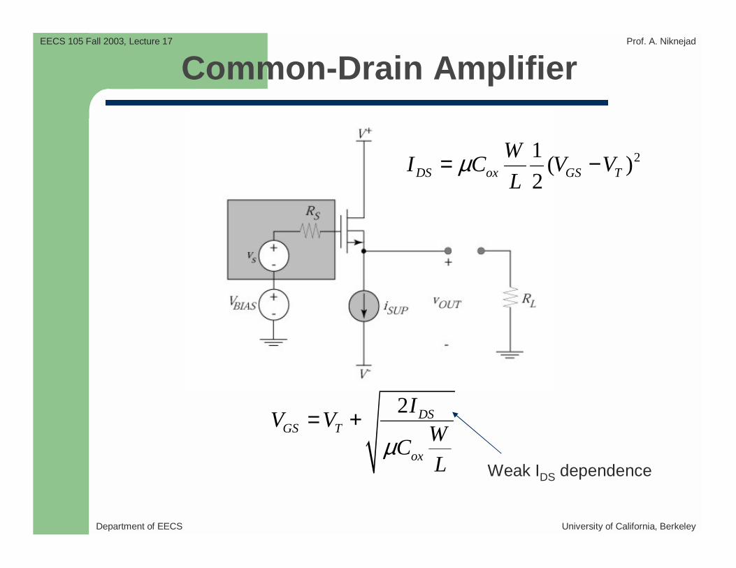
Common-Drain Amplifier
21( )
2DS ox GS T
WI C V V
Lµ= −
2 DSGS T
ox
IV V
WC
Lµ
= +
Weak IDS dependence
Department of EECS University of California, Berkeley
EECS 105 Fall 2003, Lecture 17 Prof. A. Niknejad
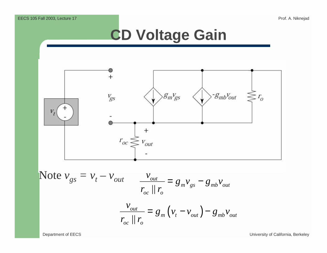
CD Voltage Gain
Note vgs = vt – vout||
outm gs mb out
oc o
vg v g v
r r= −
( )||
outm t out mb out
oc o
vg v v g v
r r= − −

Department of EECS University of California, Berkeley
EECS 105 Fall 2003, Lecture 17 Prof. A. Niknejad
CD Voltage Gain (Cont.)
KCL at source node:
Voltage gain (for vSB not zero):
( )||
outm t out mb out
oc o
vg v v g v
r r= − −
1
|| mb m out m toc o
g g v g vr r
+ + =
1||
out m
inmb m
oc o
v g
v g gr r
=+ +
1out m
in mb m
v g
v g g≈ ≈
+
Department of EECS University of California, Berkeley
EECS 105 Fall 2003, Lecture 17 Prof. A. Niknejad
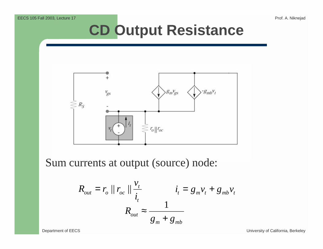
CD Output Resistance
Sum currents at output (source) node:
|| || tout o oc
t
vR r r
i= t m t mb ti g v g v= +
1out
m mb
Rg g
≈+
Department of EECS University of California, Berkeley
EECS 105 Fall 2003, Lecture 17 Prof. A. Niknejad
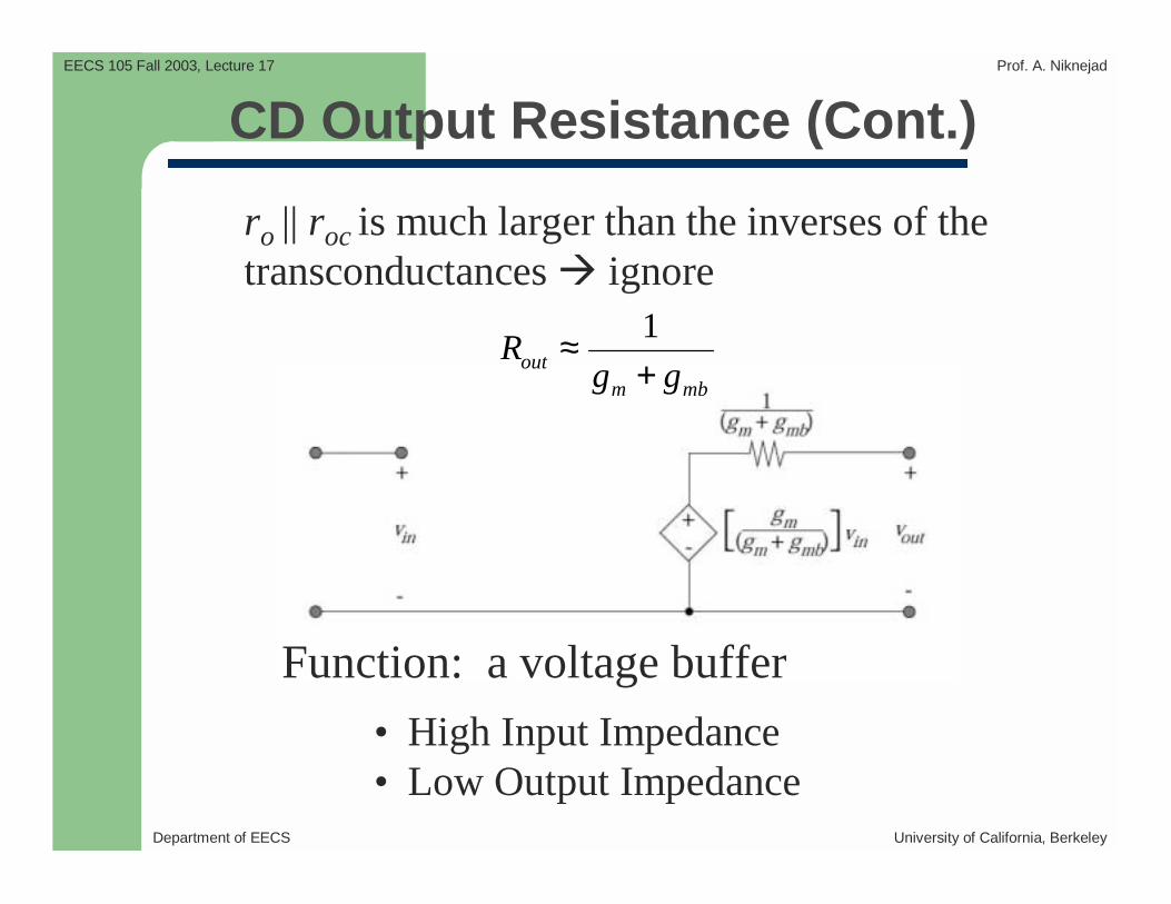
CD Output Resistance (Cont.)
ro || roc is much larger than the inverses of the transconductances ignore
1out
m mb
Rg g
≈+
Function: a voltage buffer
• High Input Impedance• Low Output Impedance
Department of EECS University of California, Berkeley
EECS 105 Fall 2003, Lecture 17 Prof. A. Niknejad