Embed Size (px)
DESCRIPTION
Lecture-15 BJT
Citation preview
The inner junction capacitances are shown in Fig. They are not physically connected but inherently present with the device.
1
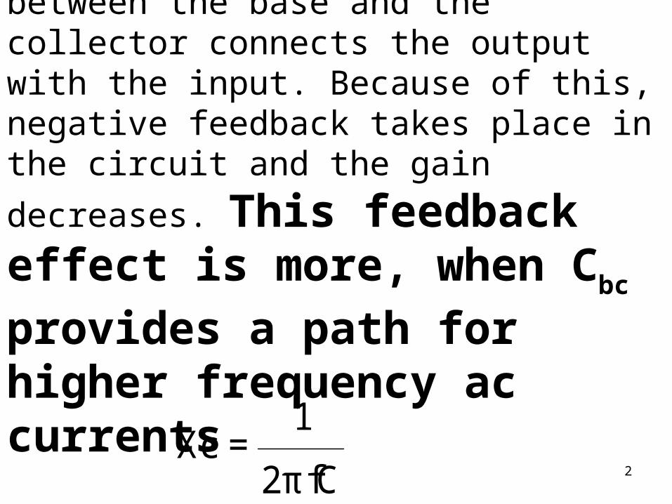
The capacitor Cbc between the base and the collector connects the output with the input. Because of this, negative feedback takes place in the
circuit and the gain decreases. This feedback effect is more, when Cbc provides a path for higher
frequency ac currents1
Xc =2πfC 2
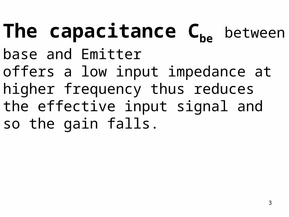
The capacitance Cbe between base
and Emitteroffers a low input impedance at higher frequency thus reduces the effective input signal and so the gain falls.
3
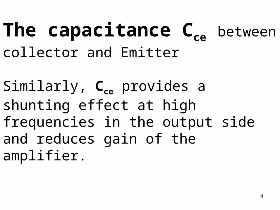
The capacitance Cce between
collector and Emitter
Similarly, Cce provides a shunting effect at high frequencies in the output side and reduces gain of the amplifier.
4
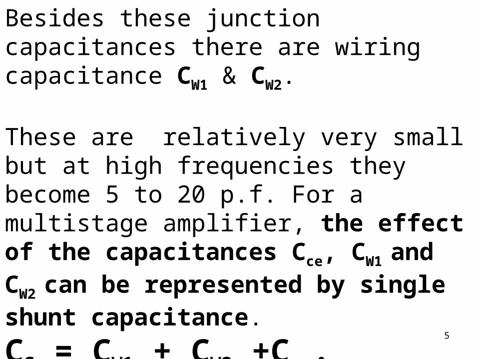
Besides these junction capacitances there are wiring capacitance CW1 & CW2.
These are relatively very small but at high frequencies they become 5 to 20 p.f. For a multistage amplifier, the effect of the capacitances Cce, CW1 and CW2 can be represented by single shunt capacitance.
CS = CW1 + CW2 +Cce.5
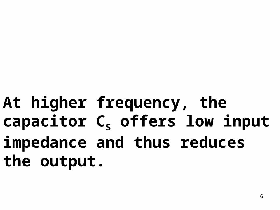
At higher frequency, the capacitor CS offers low input impedance and thus reduces the output.
6
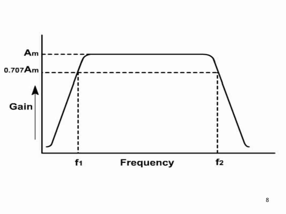
The gain is constant over a frequency
range. The frequencies at which the gain reduces to 70.7% of the maximum gain are known as cut off frequencies, there are upper cut off frequency and lower cut off frequency.
Bandwidth of an amplifier (BW)
7
8
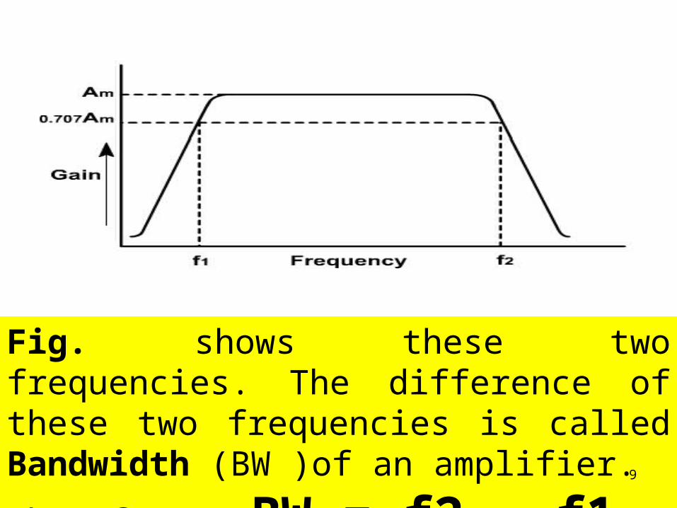
Fig. shows these two frequencies. The difference of these two frequencies is called Bandwidth (BW )of an amplifier.
Therefore BW = f2 – f1. 9
At f1 and f2, the gain voltage becomes 70.7% i.e. (Am / 2). The output voltage reduces to (1 / 2 )of maximum output voltage.
Since the power is proportional to voltage square the output power at these frequencies becomes half maximum power.
The gain on dB scale is given by
10
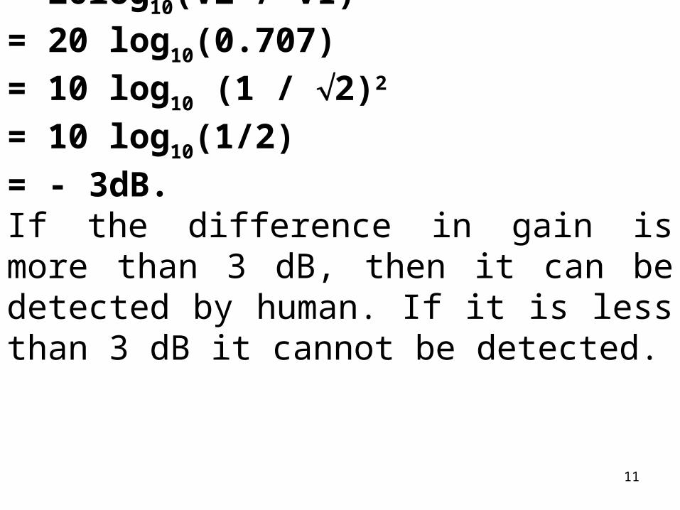
20log10(V2 / V1)
= 20 log10(0.707)
= 10 log10 (1 / 2)2
= 10 log10(1/2)
= - 3dB.If the difference in gain is more than 3 dB, then it can be detected by human. If it is less than 3 dB it cannot be detected.
11

Finding the two Cutoff Frequencies
12
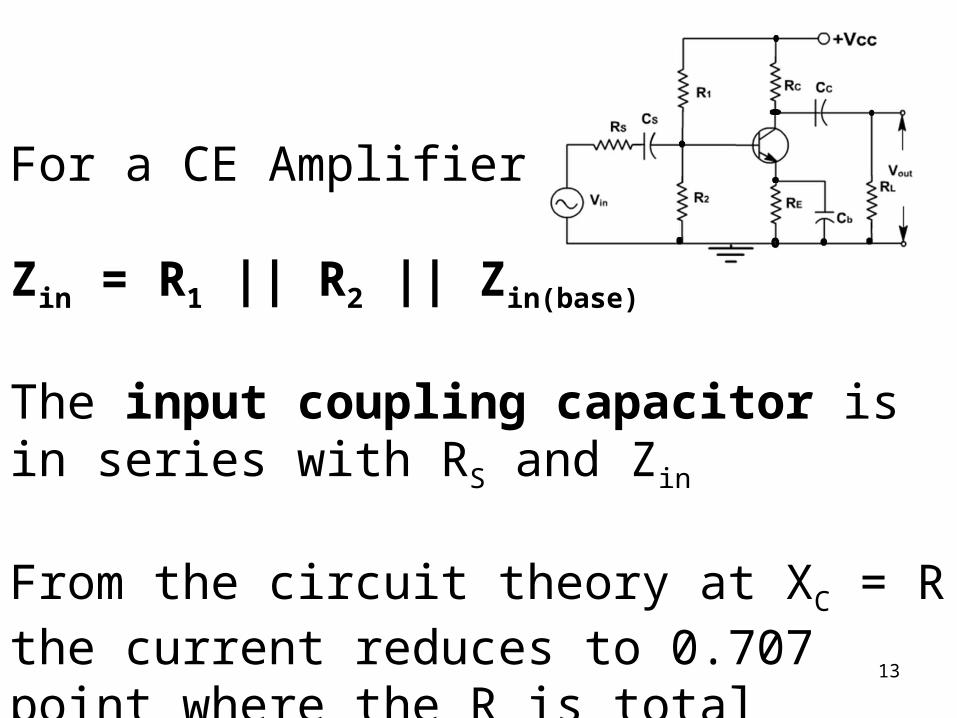
For a CE Amplifier
Zin = R1 || R2 || Zin(base)
The input coupling capacitor is in series with RS and Zin
From the circuit theory at XC = R the current reduces to 0.707 point where the R is total series resistance
13
14
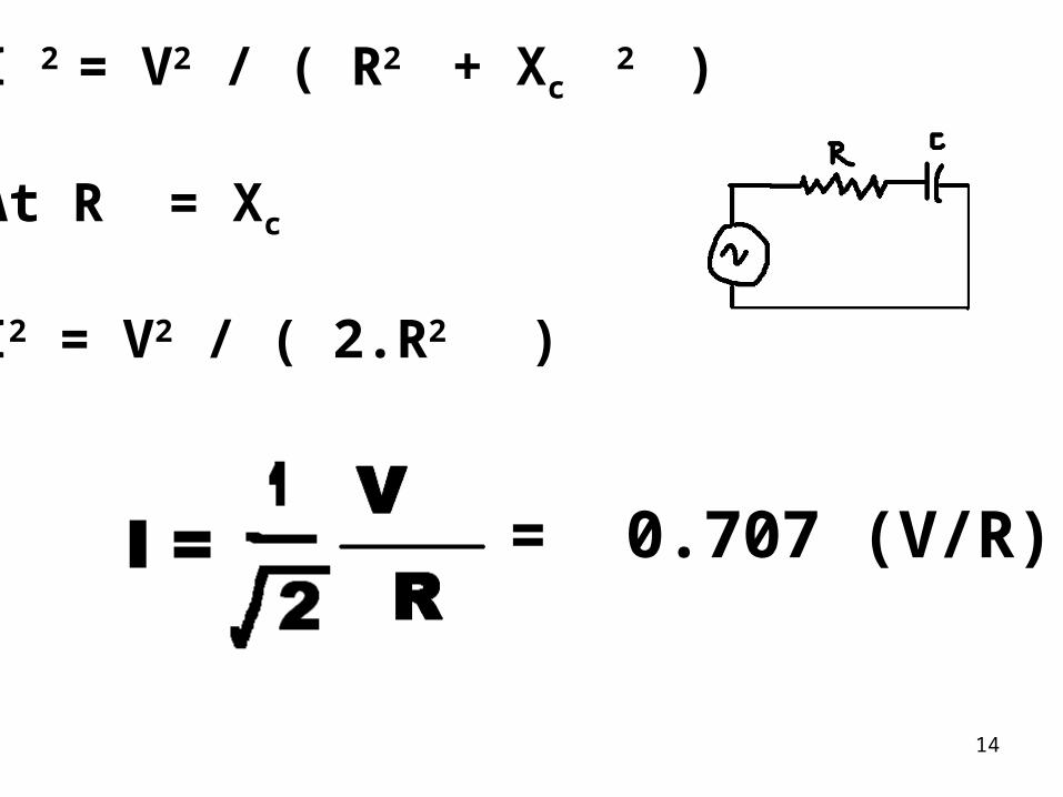
I 2 = V2 / ( R2 + Xc 2 )
At R = Xc
I2 = V2 / ( 2.R2 )
= 0.707 (V/R)
Therefore
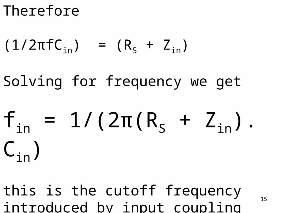
(1/2πfCin) = (RS + Zin)
Solving for frequency we get
fin = 1/(2π(RS + Zin). Cin)
this is the cutoff frequency introduced by input coupling capacitor
15
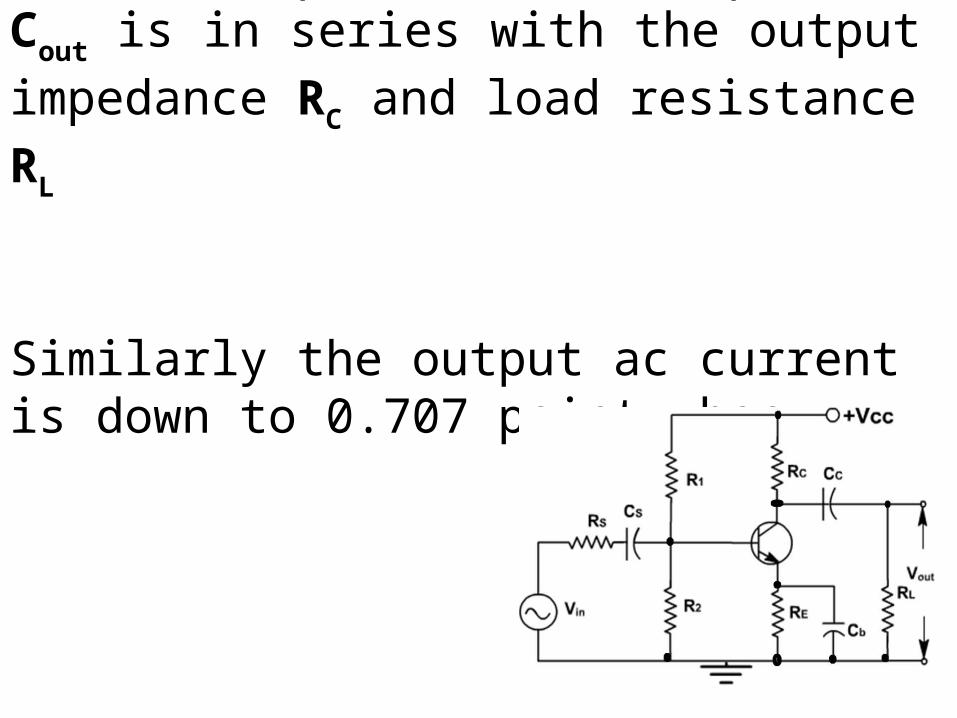
on the output side the capacitor Cout is in series with the output impedance RC and load resistance RL
Similarly the output ac current is down to 0.707 point when
XC = R
16
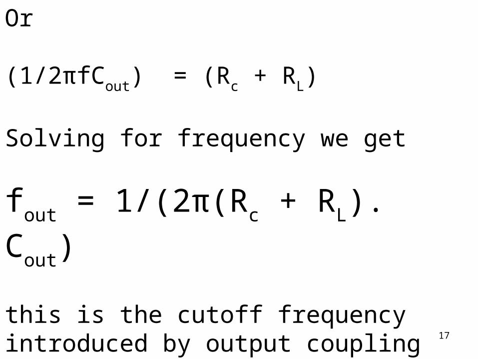
Or
(1/2πfCout) = (Rc + RL)
Solving for frequency we get
fout = 1/(2π(Rc + RL). Cout)
this is the cutoff frequency introduced by output coupling capacitor
17
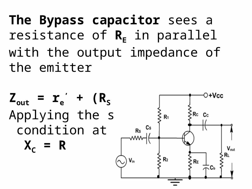
The Bypass capacitor sees a resistance of RE in parallel with the output impedance of the emitter
Zout = re’ + (RS || R1 || R2)/β
Applying the same condition at XC = R
18
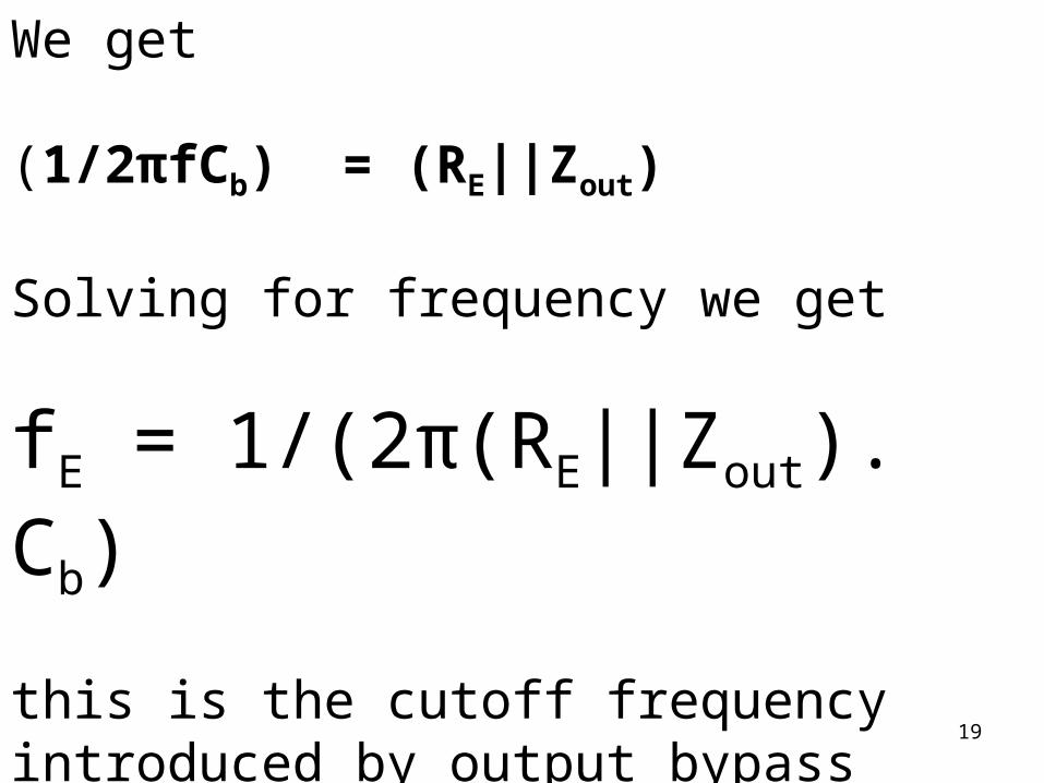
We get
(1/2πfCb) = (RE||Zout)
Solving for frequency we get
fE = 1/(2π(RE||Zout). Cb)
this is the cutoff frequency introduced by output bypass capacitor
19
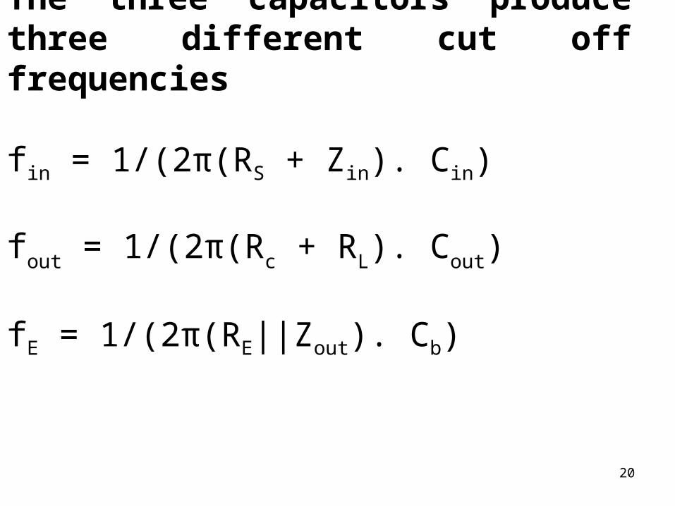
The three capacitors produce three different cut off frequencies
fin = 1/(2π(RS + Zin). Cin)
fout = 1/(2π(Rc + RL). Cout)
fE = 1/(2π(RE||Zout). Cb)
20
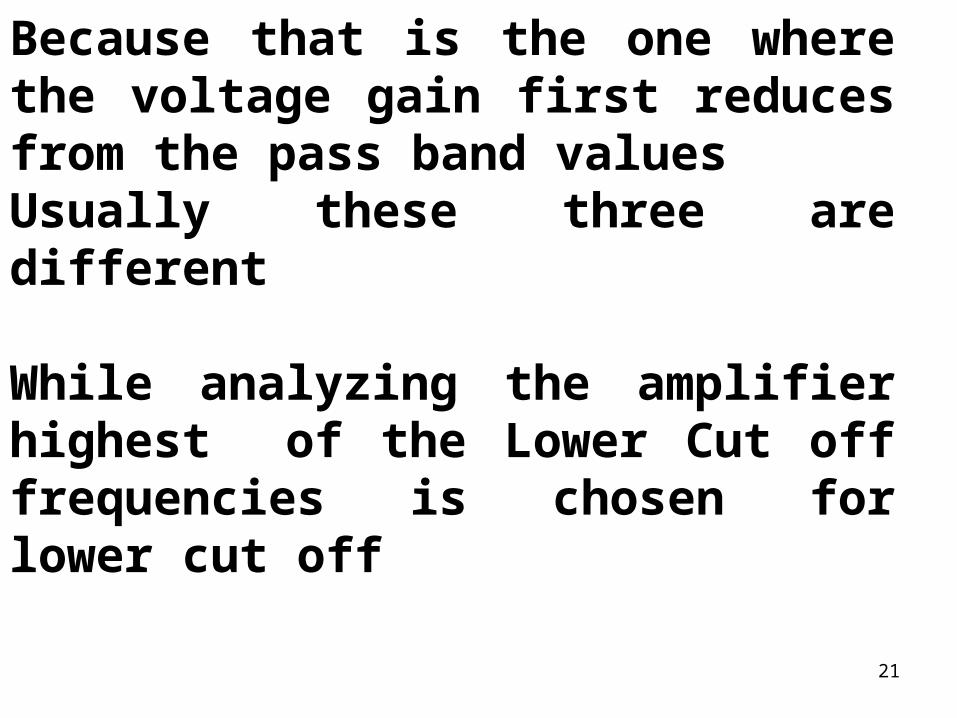
The highest one is most criticalBecause that is the one where the voltage gain first reduces from the pass band valuesUsually these three are different
While analyzing the amplifier highest of the Lower Cut off frequencies is chosen for lower cut off
21
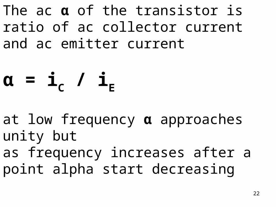
The ac α of the transistor is ratio of ac collector current and ac emitter current
α = iC / iE
at low frequency α approaches unity but as frequency increases after a point alpha start decreasing
22
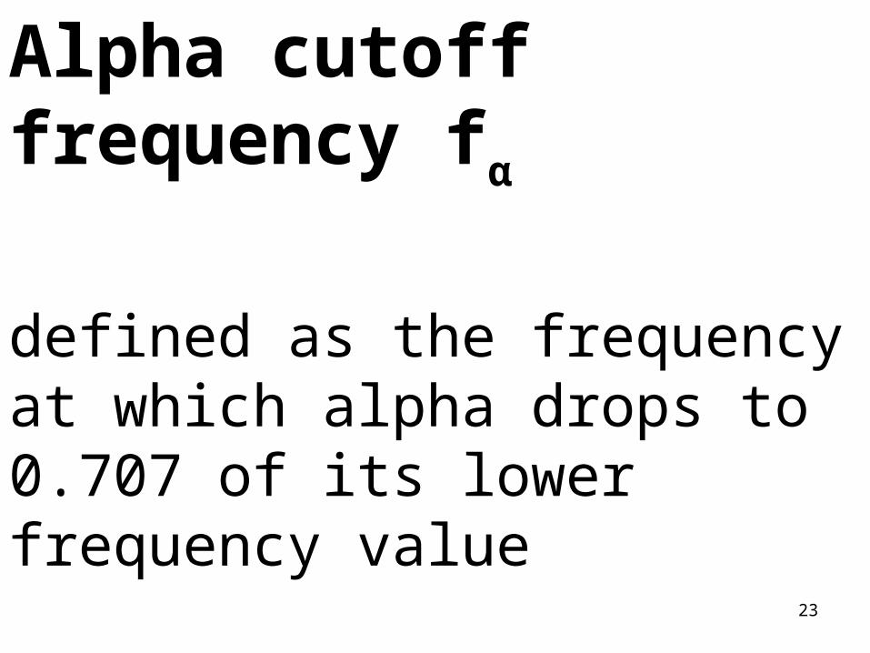
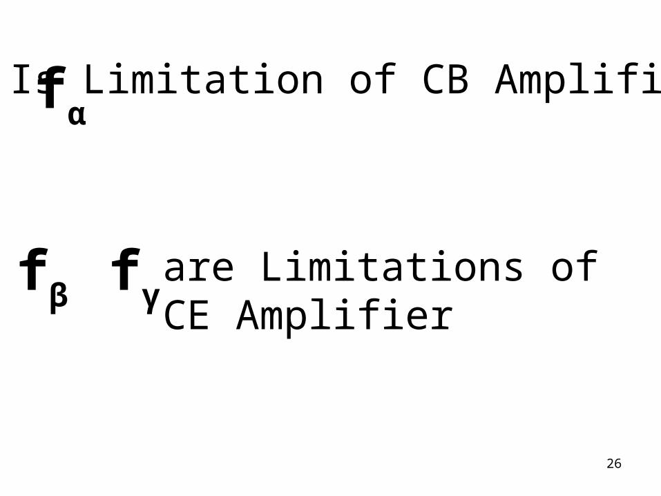
Alpha cutoff frequency fα
defined as the frequency at which alpha drops to 0.707 of its lower frequency value
fα is one of the limitation in CB amplifier 23
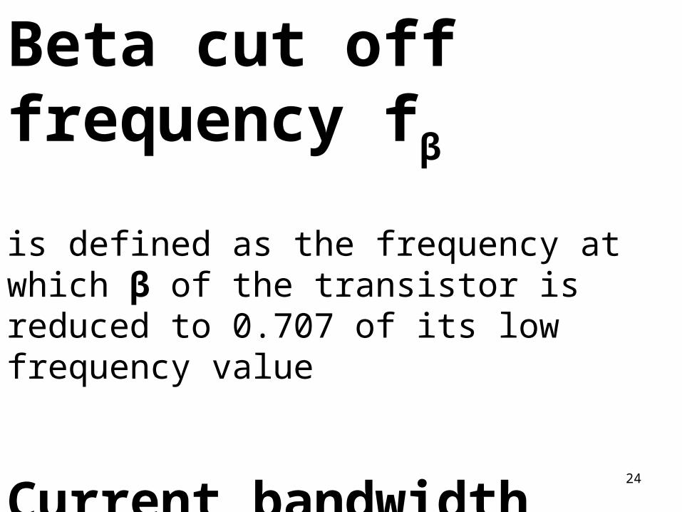
Beta cut off frequency fβ
is defined as the frequency at which β of the transistor is reduced to 0.707 of its low frequency value
Current bandwidth product fγ
is defined as frequency at which β equals unity24
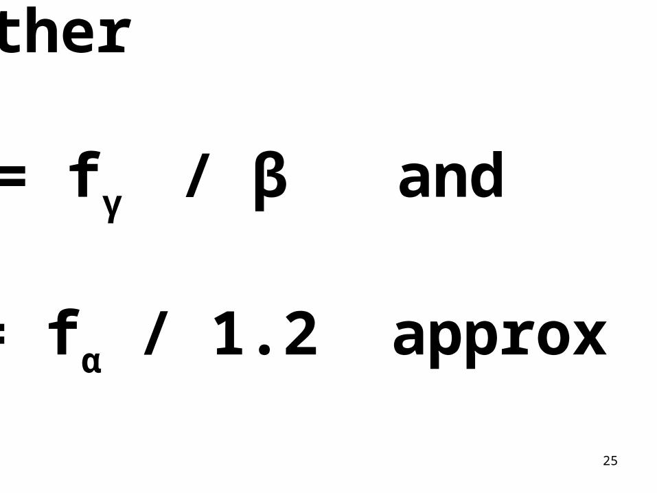
Further
fβ = fγ / β and
fγ = fα / 1.2 approx
25
26
fαIs Limitation of CB Amplifier
, are Limitations of CE Amplifier
fβ fγ
h- Parameters
27
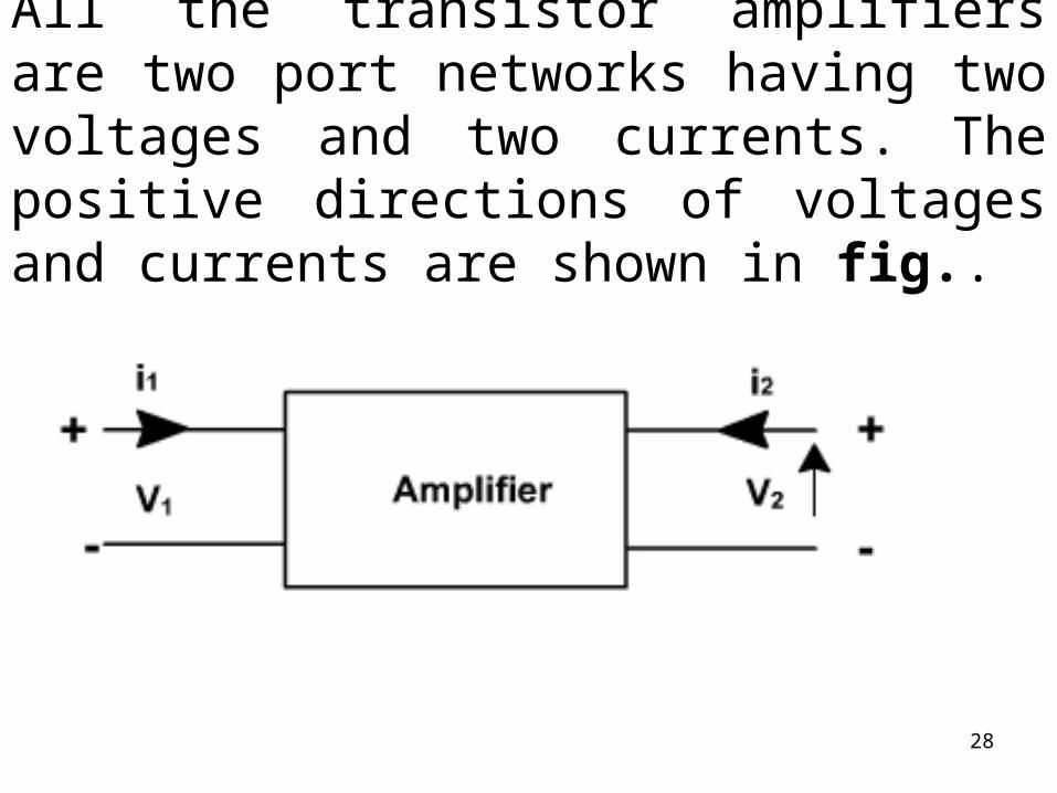
All the transistor amplifiers are two port networks having two voltages and two currents. The positive directions of voltages and currents are shown in fig..
28
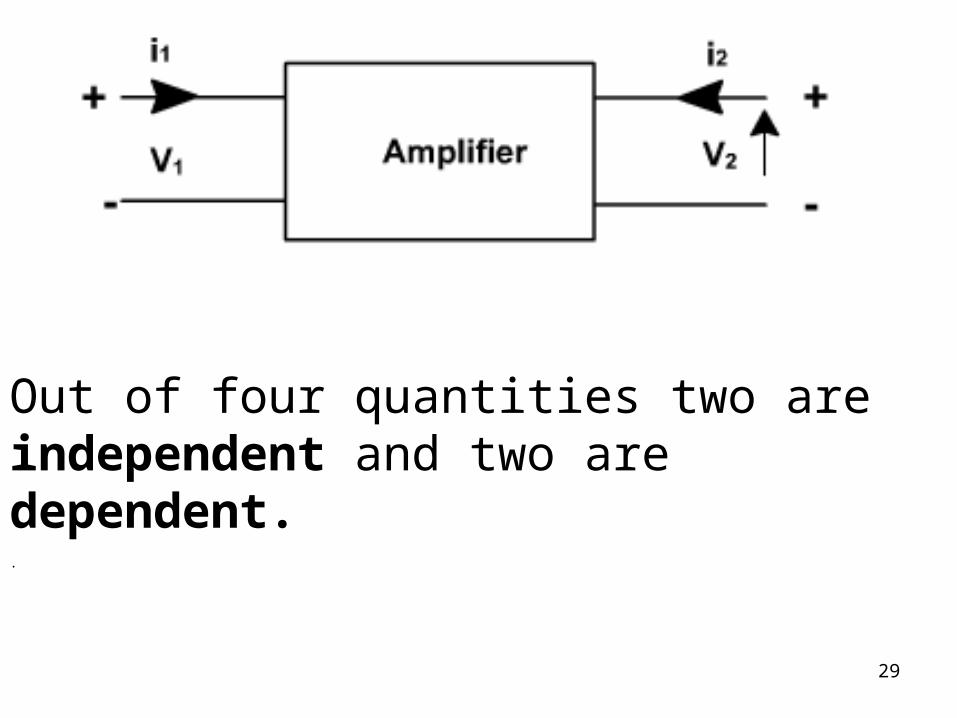
Out of four quantities two are independent and two are dependent. .
29
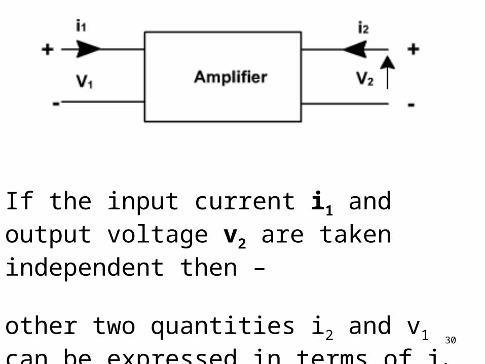
If the input current i1 and output voltage v2 are taken independent then –
other two quantities i2 and v1 can be expressed in terms of i1 and v2.
30
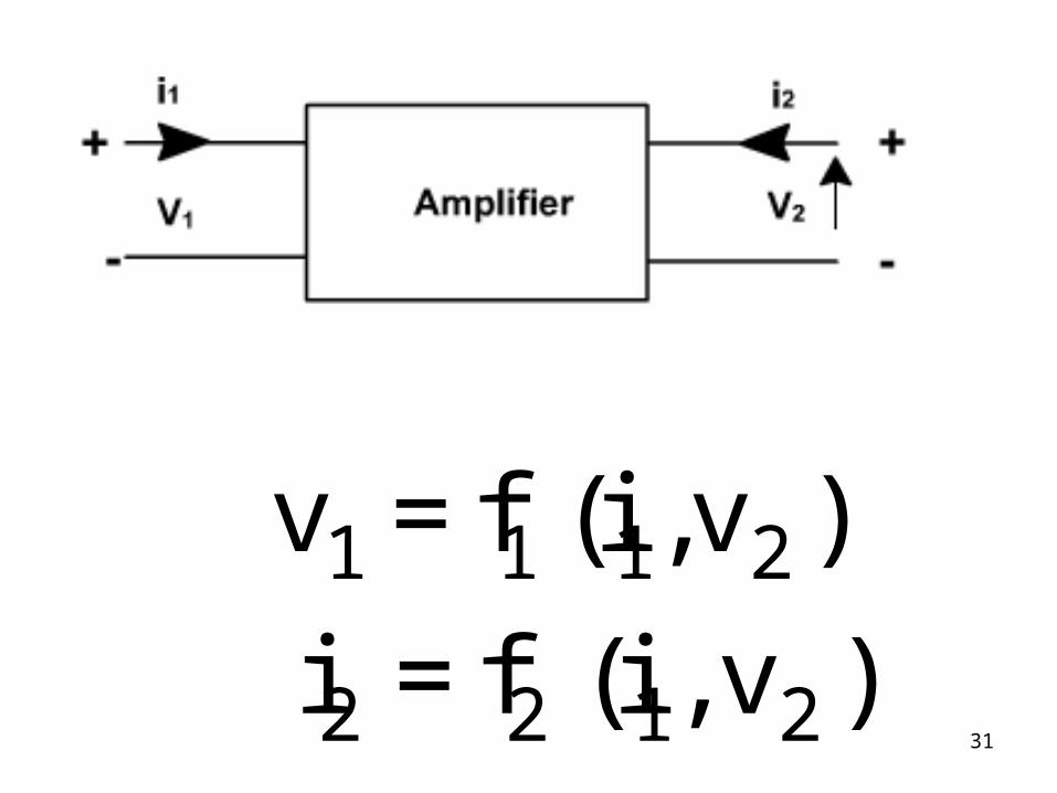
1 1 1 2
2 2 1 2
v = f (i ,v )
i = f (i , v )31
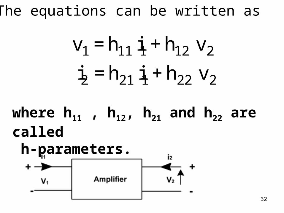
The equations can be written as
1 11 1 12 2
2 21 1 22 2
v = h i + h v
i = h i + h v
where h11 , h12, h21 and h22 are called h-parameters.
32
33
Defining
h11
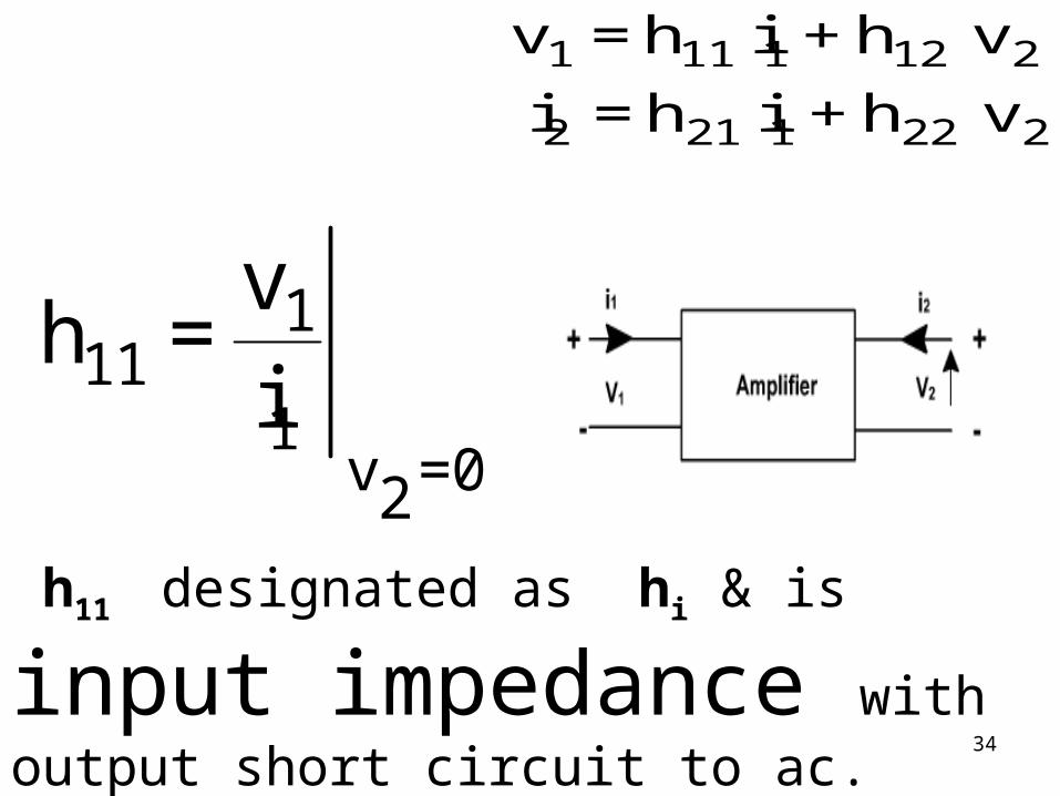
111
1v =02
vh =
i
h11 designated as hi & is
input impedance with output short circuit to ac.
1 11 1 12 2
2 21 1 22 2
v = h i + h v
i = h i + h v
34

35
Defining
h12
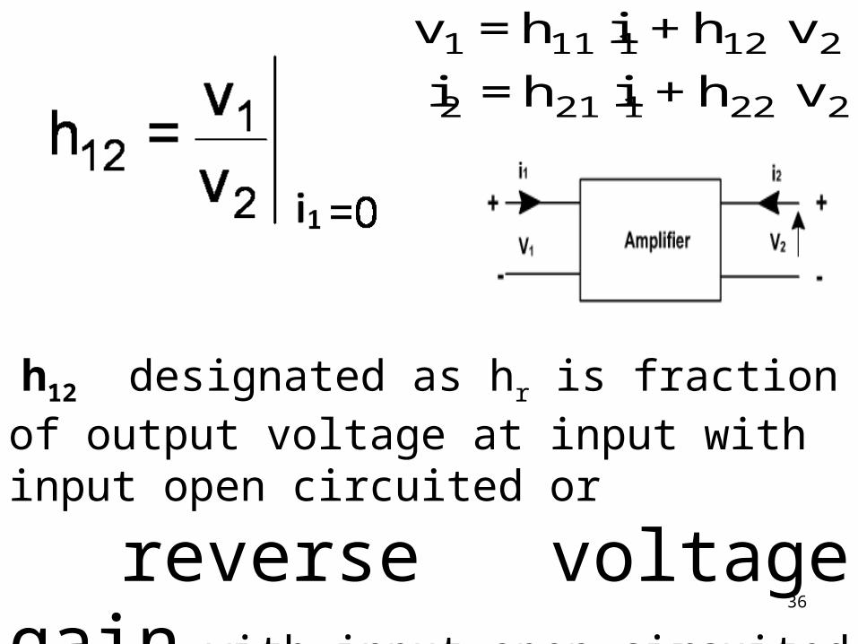
h12 designated as hr is fraction of output voltage at input with input open circuited or
reverse voltage gain with input open circuited to ac (dimensionless)
1 11 1 12 2
2 21 1 22 2
v = h i + h v
i = h i + h v
36
37
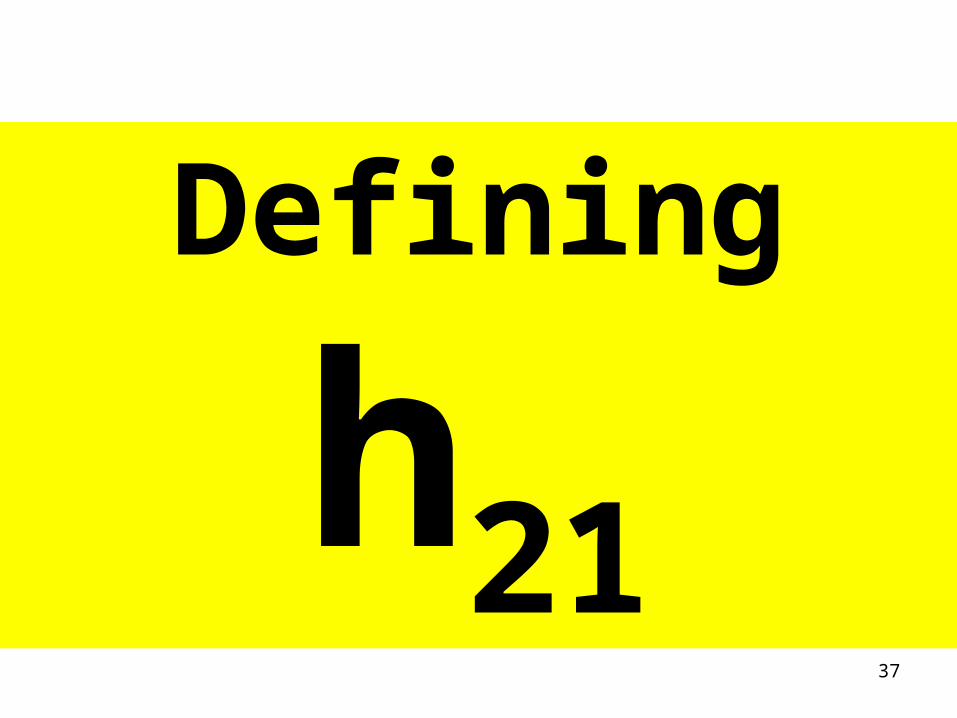
Defining
h21
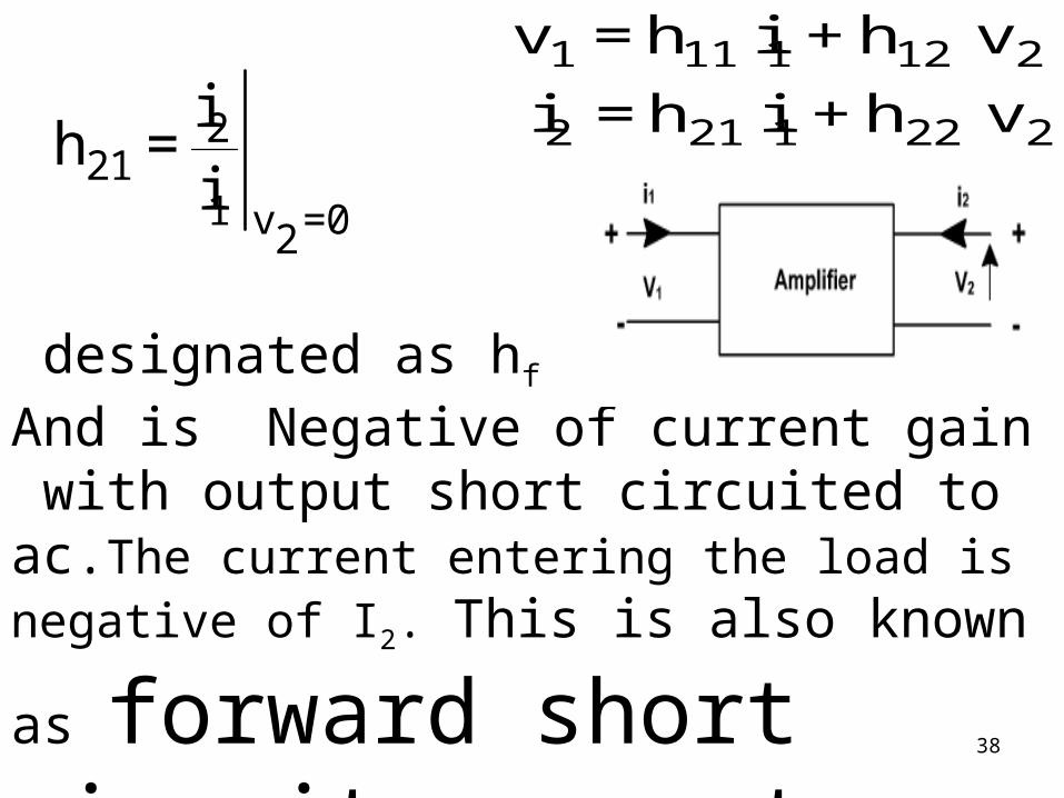
221
1 v =02
ih =
i
designated as hf And is Negative of current gain with output short circuited to ac.The current entering the load is negative of I2. This is also known as
forward short circuit current gain.
1 11 1 12 2
2 21 1 22 2
v = h i + h v
i = h i + h v
38
39
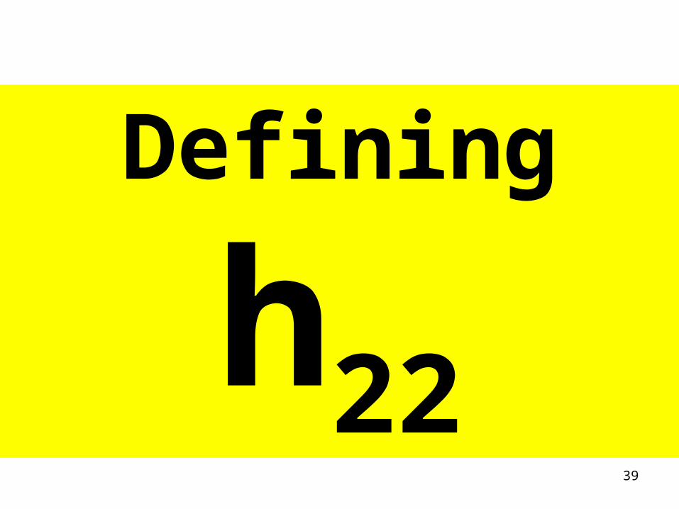
Defining
h22
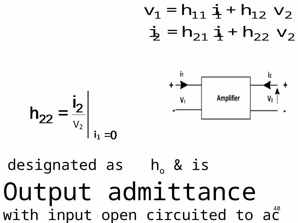
designated as ho & is
Output admittance with input open circuited to ac
1 11 1 12 2
2 21 1 22 2
v = h i + h v
i = h i + h v
40
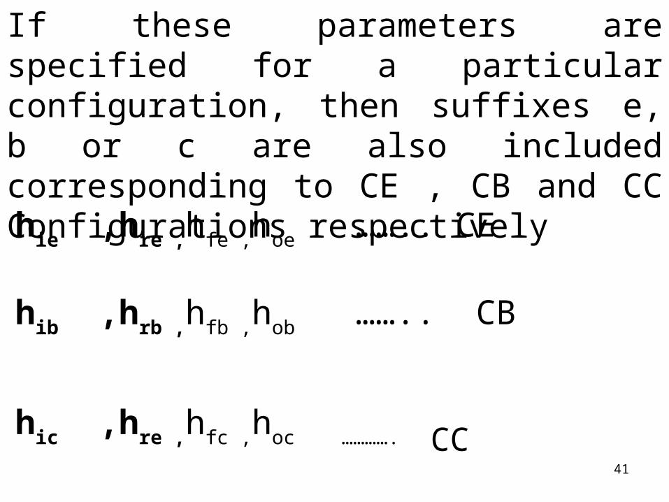
If these parameters are specified for a particular configuration, then suffixes e, b or c are also included corresponding to CE , CB and CC Configurations respectively
hie ,hre ,hfe ,hoe …….. CE hib ,hrb ,hfb ,hob …….. CB
hic ,hre ,hfc ,hoc …………. CC41
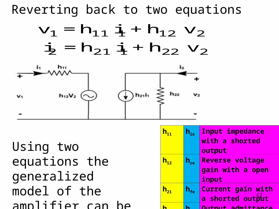
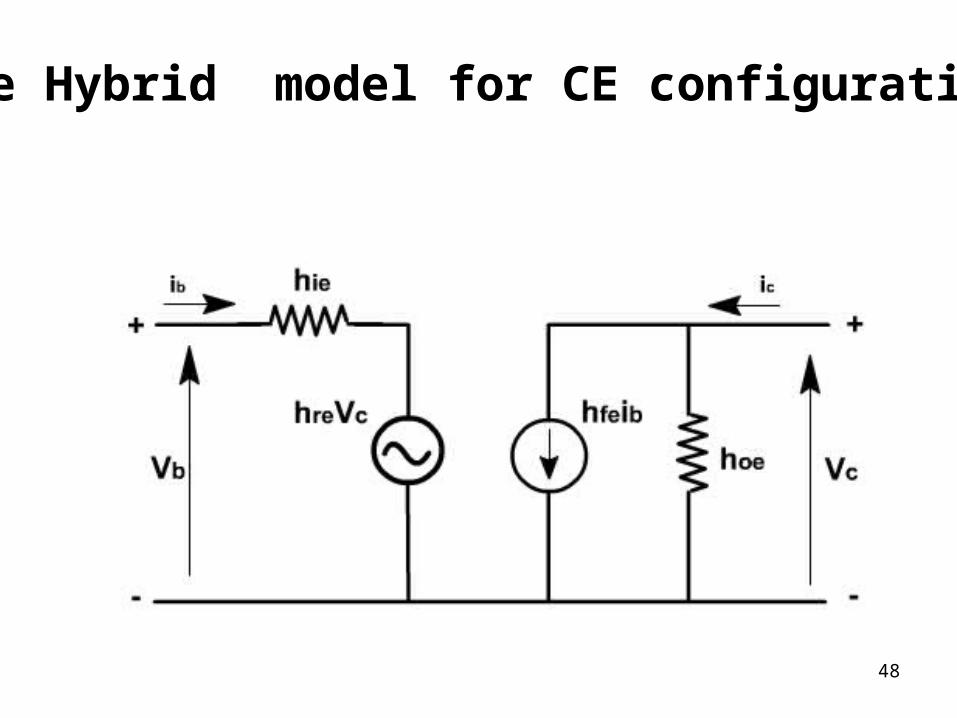
Using two equations the generalized model of the amplifier can be drawn as shown in fig.
1 11 1 12 2
2 21 1 22 2
v = h i + h v
i = h i + h v
Reverting back to two equations
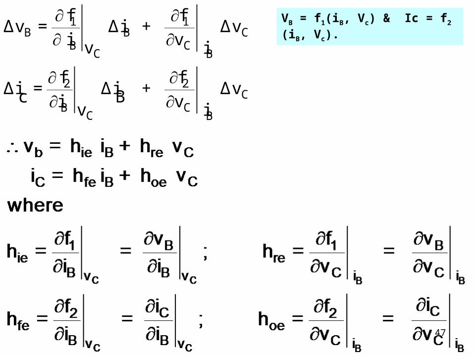
h11 hie Input impedance with a shorted output
h12 hre Reverse voltage gain with a open input
h21 hfe Current gain with a shorted output
h22 hoe Output admittance with an open input 42
hybrid model for a transistor amplifier
43
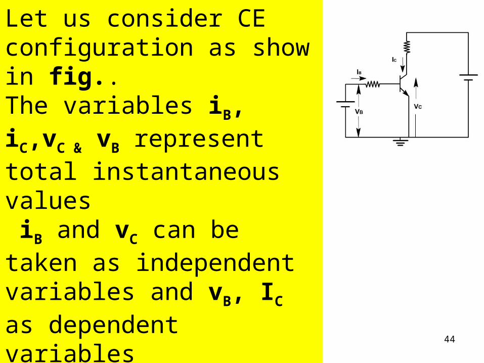
Let us consider CE configuration as show in fig.. The variables iB, iC,vC & vB represent total instantaneous values iB and vC can be taken as independent variables and vB, IC as dependent variables
44
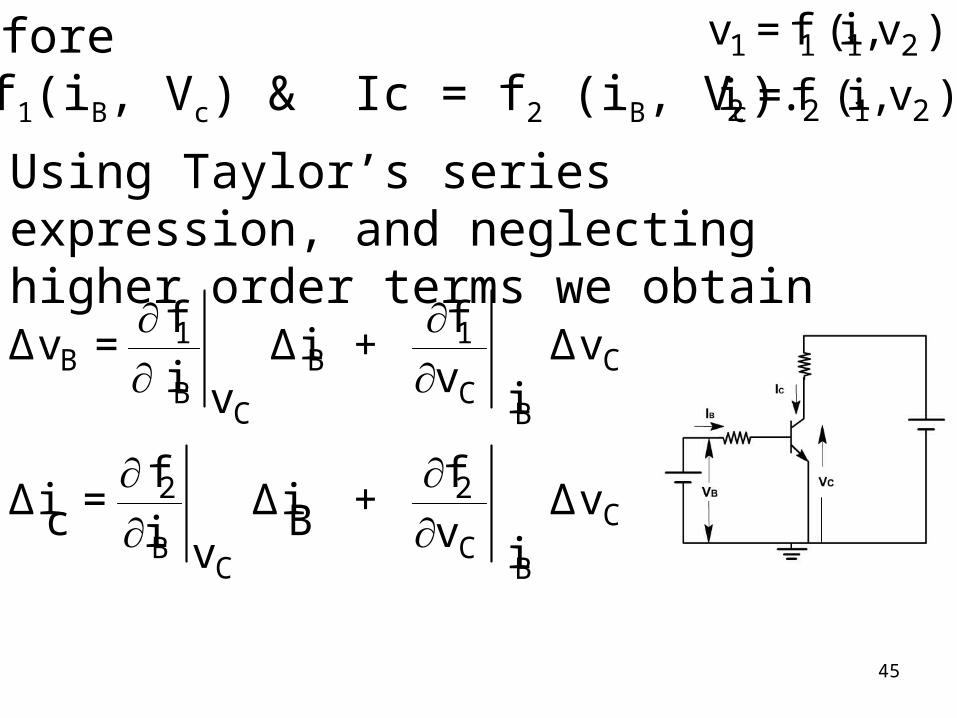
ThereforeVB = f1(iB, Vc) & Ic = f2 (iB, Vc).
1 1B B C
B CC B
2 2C
B CC B
f fΔv = Δi + Δv
i vv i
f fΔi = Δi + Δvc Bi vv i
Using Taylor’s series expression, and neglecting higher order terms we obtain
1 1 1 2
2 2 1 2
v = f (i ,v )
i = f (i , v )
45
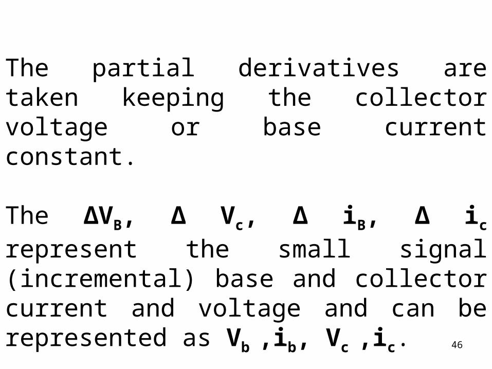
The partial derivatives are taken keeping the collector voltage or base current constant.
The ΔVB, Δ Vc, Δ iB, Δ ic represent the small signal (incremental) base and collector current and voltage and can be represented as Vb ,ib, Vc ,ic.
46
1 1B B C
B CC B
2 2C
B CC B
f fΔv = Δi + Δv
i vv i
f fΔi = Δi + Δvc Bi vv i
VB = f1(iB, Vc) & Ic = f2 (iB, Vc).
47
The Hybrid model for CE configuration
48
Determination of h - parameters
49
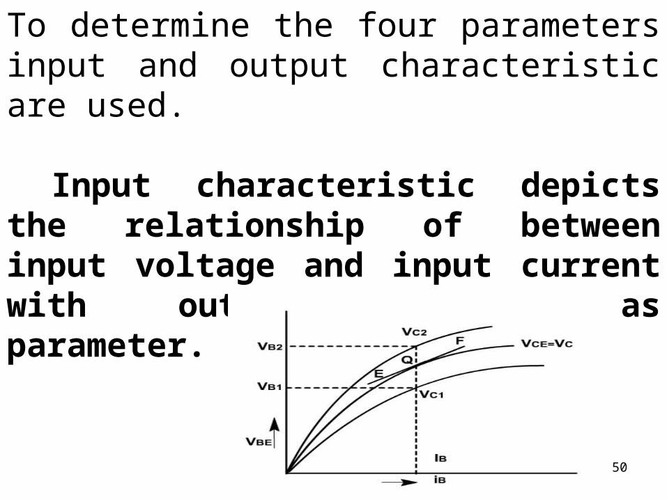
To determine the four parameters input and output characteristic are used.
Input characteristic depicts the relationship of between input voltage and input current with output voltage as parameter.
50
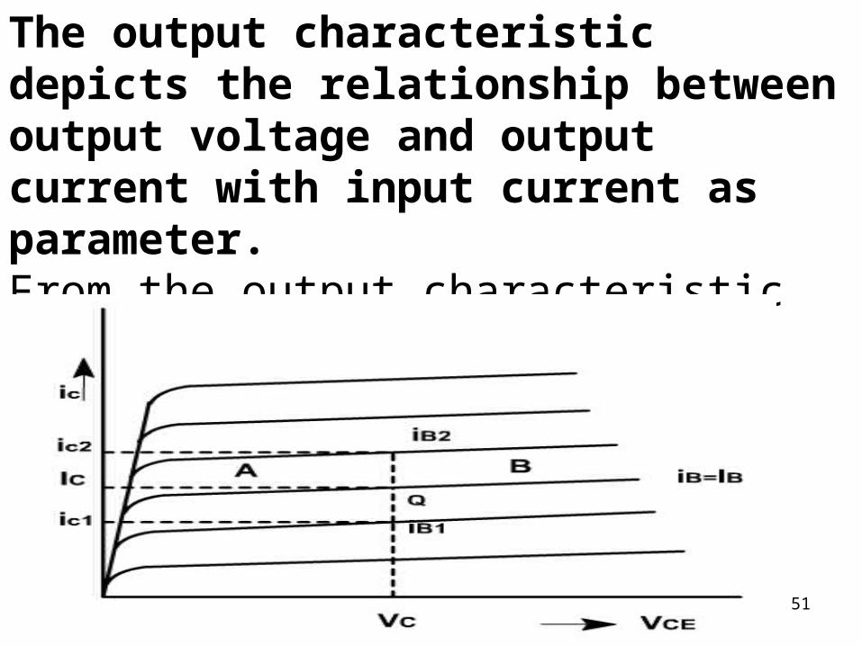
The output characteristic depicts the relationship between output voltage and output current with input current as parameter. From the output characteristic shown.
51
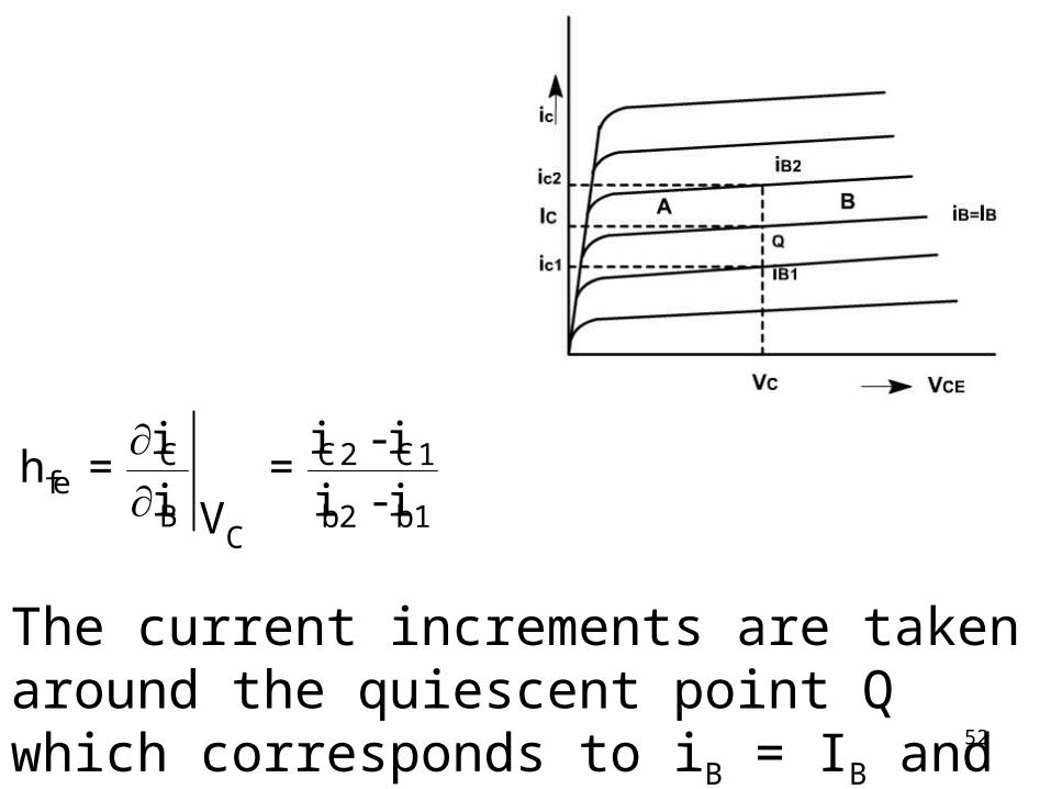
C C2 C1fe
B b2 b1C
i - iih = =
i i - iV
The current increments are taken around the quiescent point Q which corresponds to iB = IB and to the collector voltage VCE = VC
52
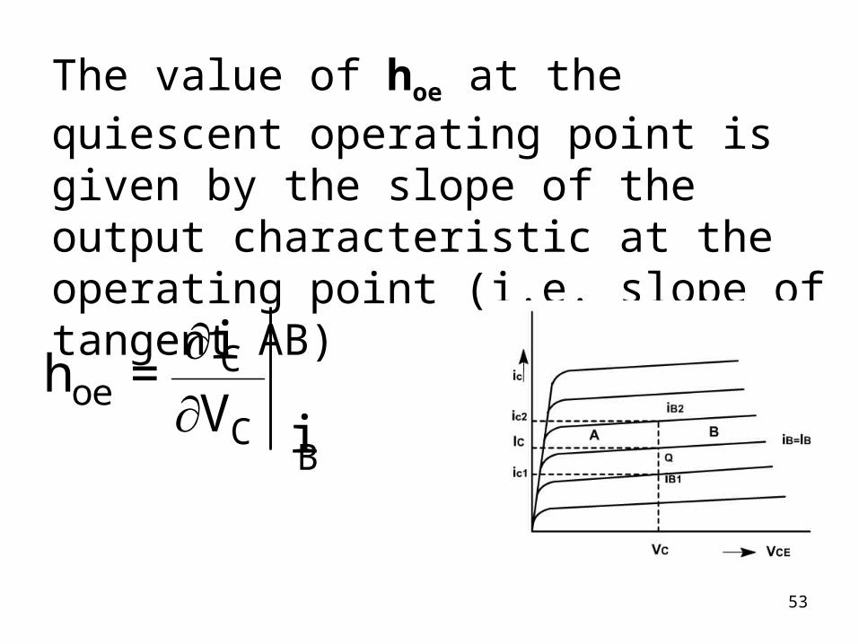
The value of hoe at the quiescent operating point is given by the slope of the output characteristic at the operating point (i.e. slope of tangent AB)
Coe
CB
ih =
V i
53
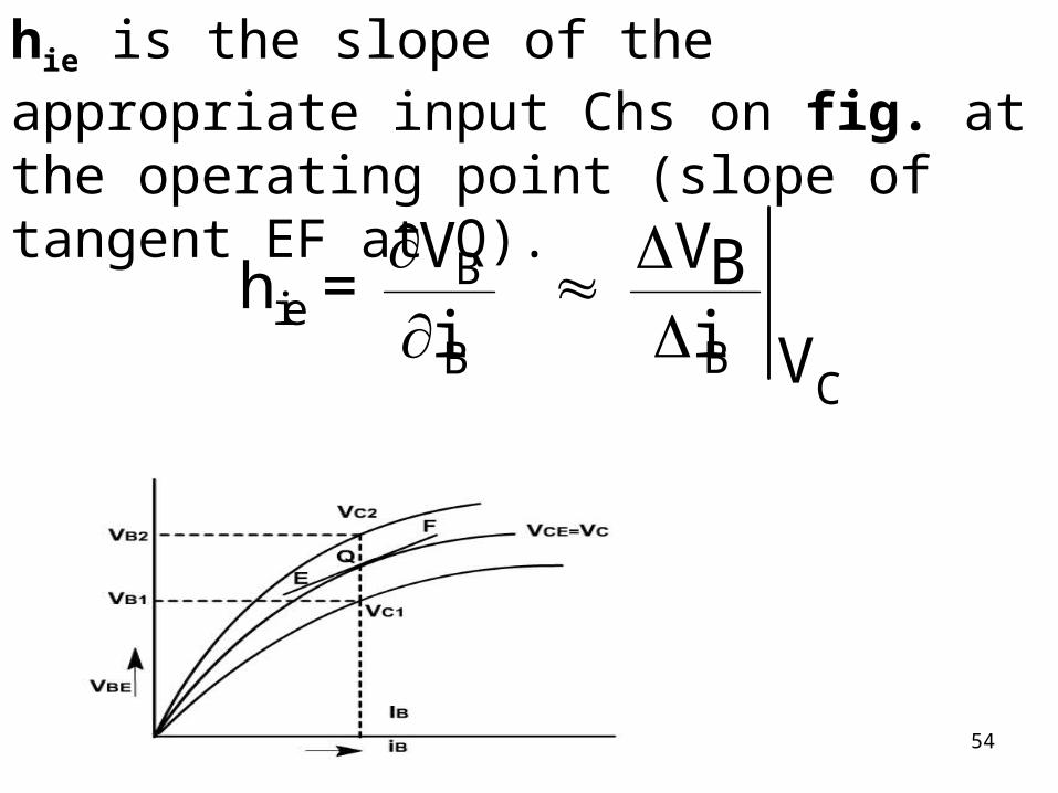
hie is the slope of the appropriate input Chs on fig. at the operating point (slope of tangent EF at Q).
Bie
BBC
V VBh =i i V
54
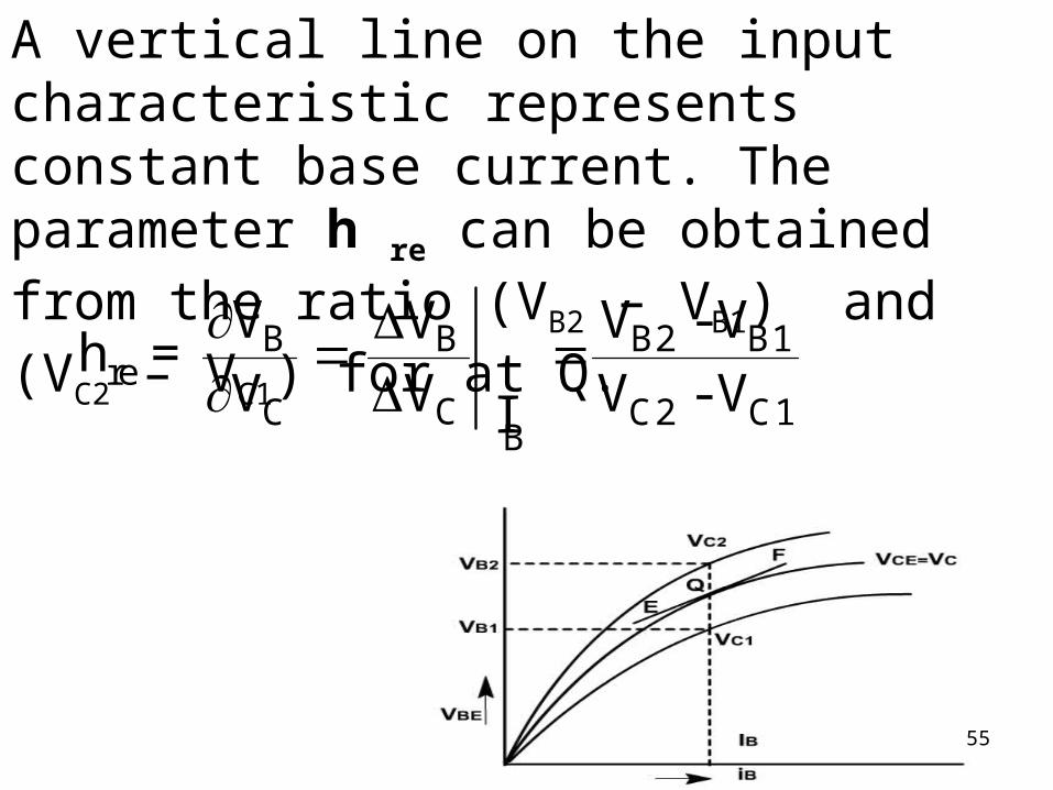
A vertical line on the input characteristic represents constant base current. The parameter h re can be obtained from the ratio (VB2 – VB1) and (VC2 – VC1) for at Q.
B B B2 B1re
CC C2 C1B
V V - VVh =
V V V - V I
55
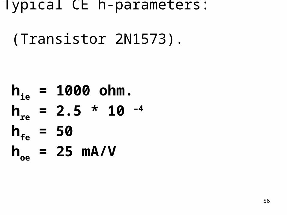
Typical CE h-parameters:
(Transistor 2N1573).
hie = 1000 ohm.
hre = 2.5 * 10 –4
hfe = 50
hoe = 25 mA/V
56
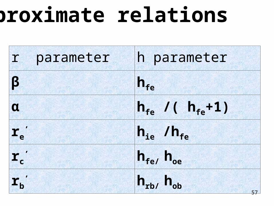
r parameter h parameter
β hfe
α hfe /( hfe+1)
re’ hie /hfe
rc’ hfe/ hoe
rb’ hrb/ hob
Approximate relations
57
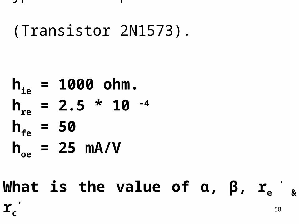
Typical CE h-parameters:
(Transistor 2N1573).
hie = 1000 ohm.
hre = 2.5 * 10 –4
hfe = 50
hoe = 25 mA/V
What is the value of α, β, re ’
& rc’
58
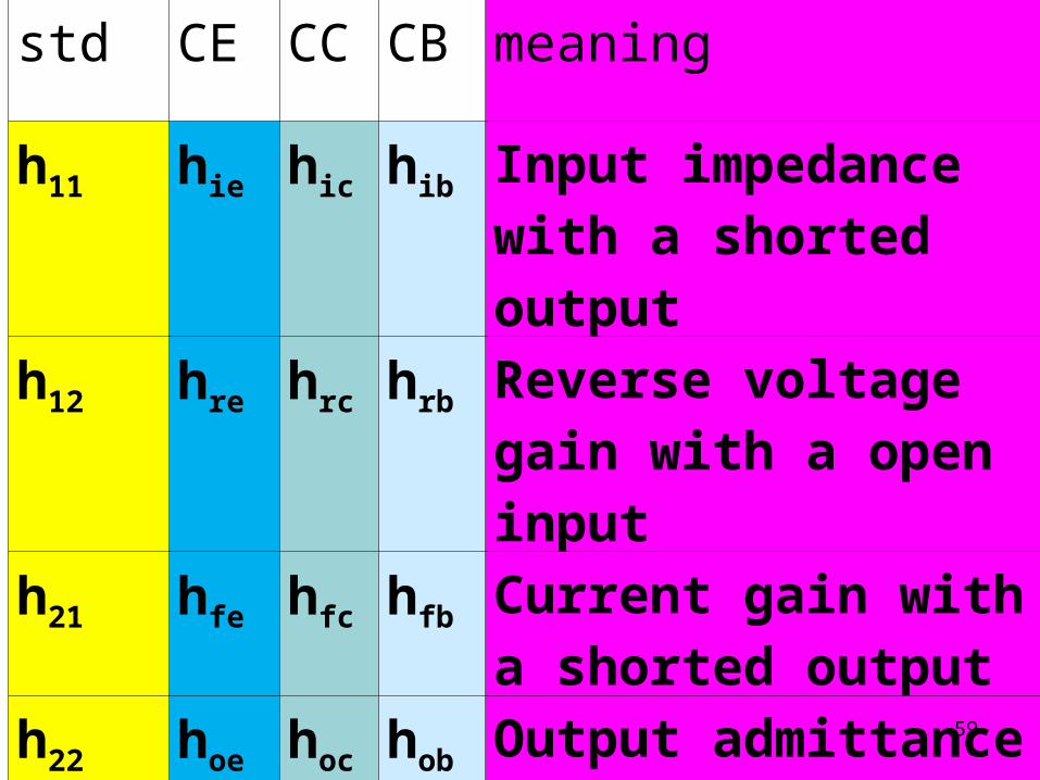
std CE CC CB meaning
h11 hie hic hib Input impedance with a shorted output
h12 hre hrc hrb Reverse voltage gain with a open input
h21 hfe hfc hfb Current gain with a shorted output
h22 hoe hoc hob Output admittance with an open input
59
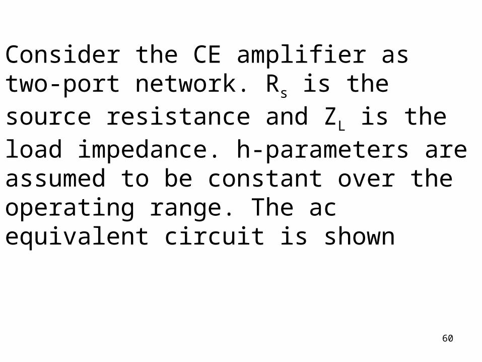
Consider the CE amplifier as two-port network. Rs is the source resistance and ZL is the load impedance. h-parameters are assumed to be constant over the operating range. The ac equivalent circuit is shown
60
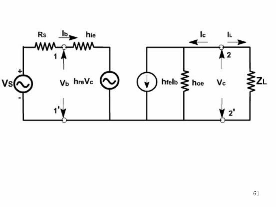
61
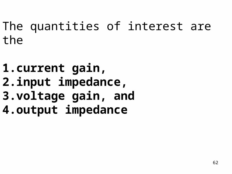
The quantities of interest are the 1.current gain, 2.input impedance, 3.voltage gain, and 4.output impedance
62
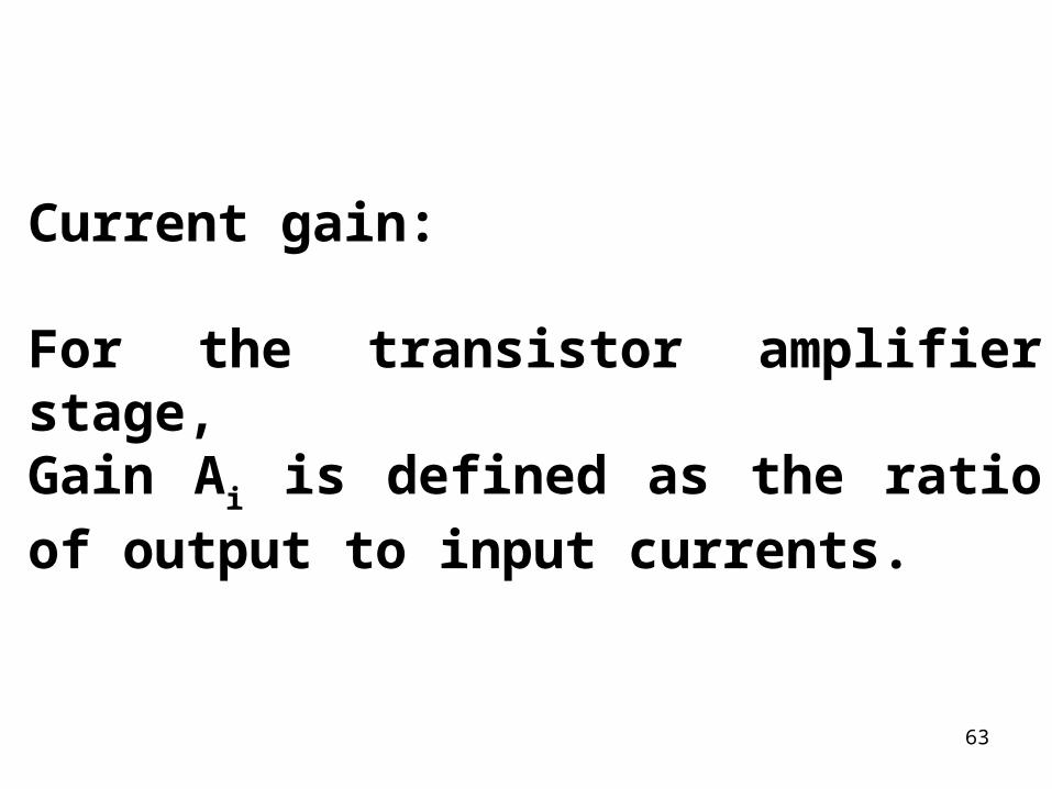
Current gain:
For the transistor amplifier stage,Gain Ai is defined as the ratio of output
to input currents.
63
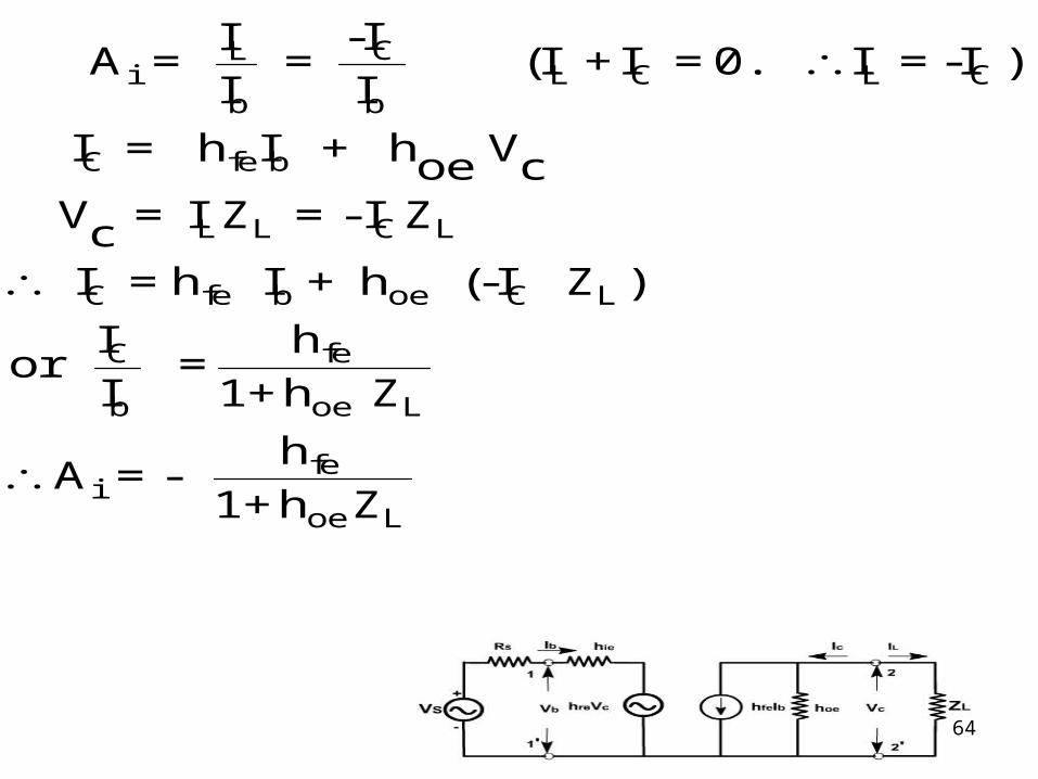
CLi L C L C
b b
C fe b
L L C L
C fe b oe C L
C fe
b oe L
fei
oe L
-IIA = = (I +I = 0. I = -I )
I I
I = h I + h Voe cV = I Z = -I ZcI = h I + h (-I Z )
I hor =
I 1+h Z
hA = -
1+h Z
64

65
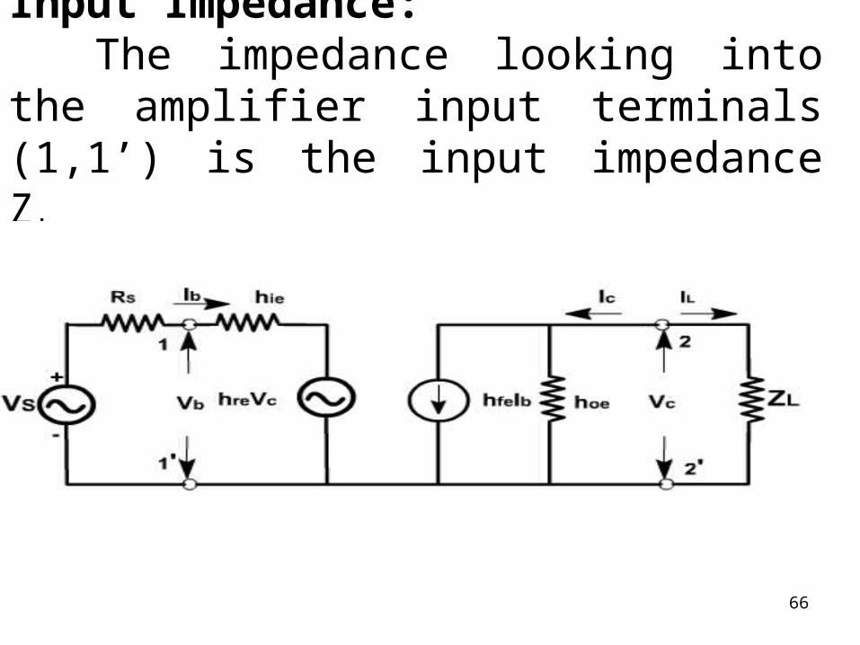
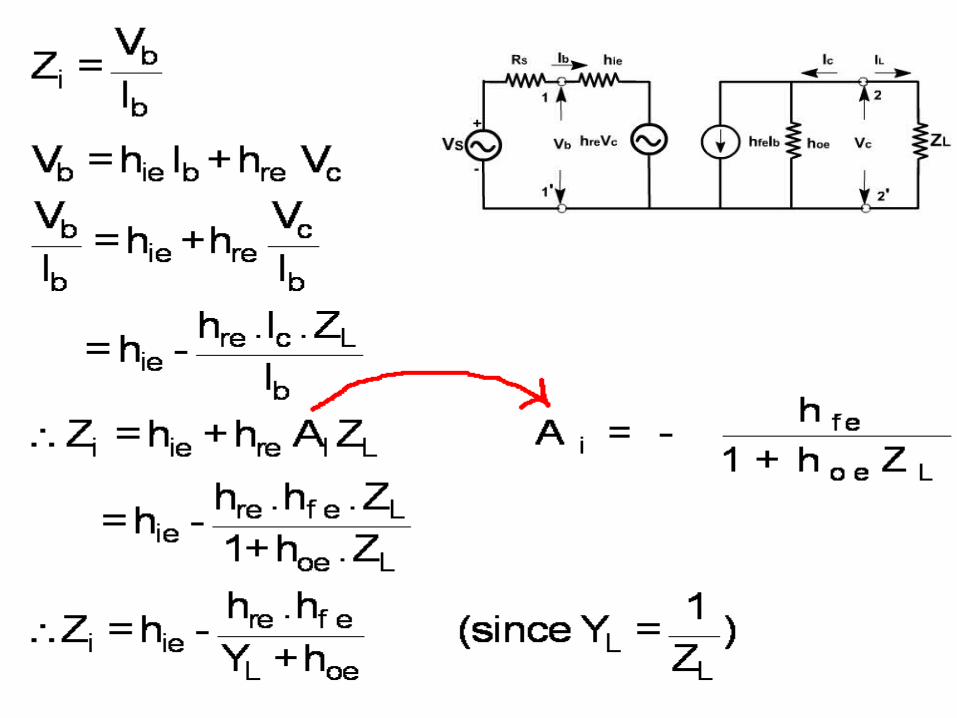
Input Impedance:The impedance looking into the
amplifier input terminals (1,1’) is the input impedance Zi
66
67
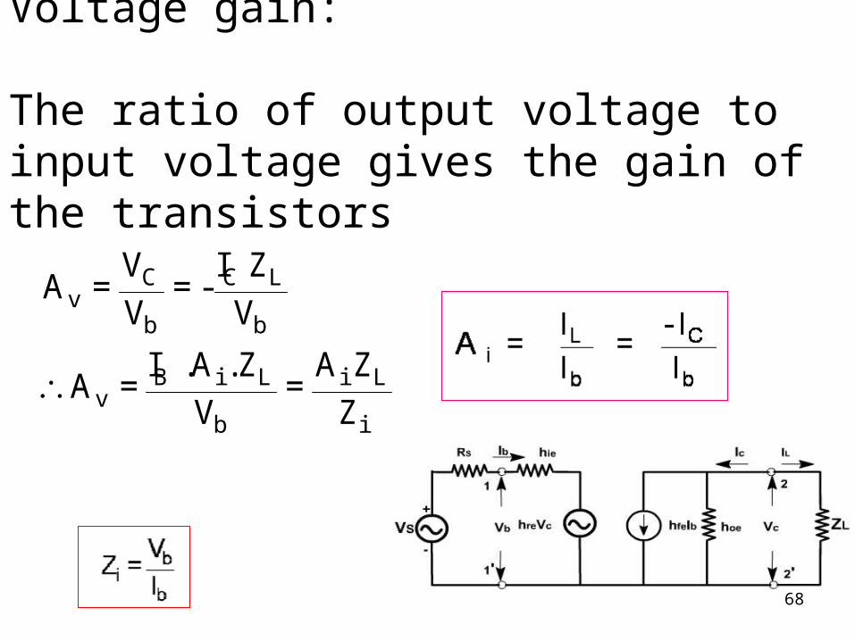
Voltage gain:
The ratio of output voltage to input voltage gives the gain of the transistors
C C Lv
b b
B i L i Lv
b i
V I ZA = = -
V V
I .A .Z A ZA = =
V Z
68
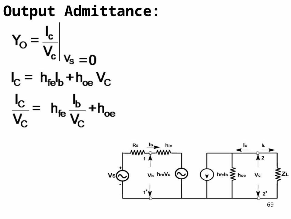
Output Admittance:
69
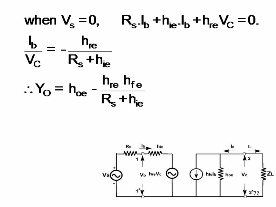
70
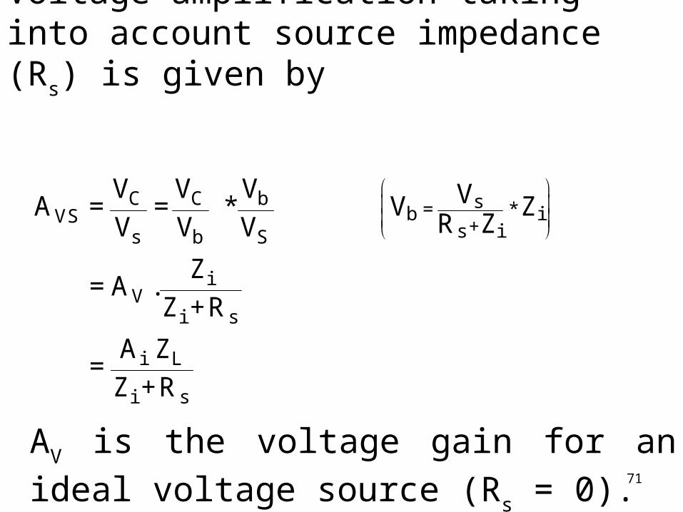
Voltage amplification taking into account source impedance (Rs) is given by
C C b s = *b iVS +s is b S
iV
i s
i L
i s
V V V VA = = * V ZR ZV V V
Z= A .
Z +R
A Z=
Z +R
AV is the voltage gain for an ideal voltage
source (Rs = 0). 71
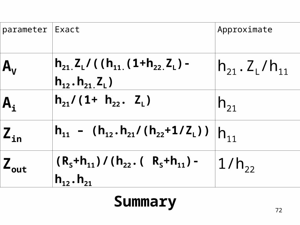
parameter Exact Approximate
AVh21.ZL/((h11.(1+h22.ZL)-h12.h21.ZL) h21.ZL/h11
Aih21/(1+ h22. ZL) h21
Zinh11 – (h12.h21/(h22+1/ZL)) h11
Zout(RS+h11)/(h22.( RS+h11)- h12.h21 1/h22
Summary72