Embed Size (px)
Citation preview

Department of EECS University of California, Berkeley
EECS 105 Fall 2003, Lecture 12
Lecture 12: MOS Transistor Models
Prof. Niknejad

Department of EECS University of California, Berkeley
EECS 105 Fall 2003, Lecture 12 Prof. A. Niknejad
Lecture Outline
� MOS Transistors (4.3 – 4.6)– I-V curve (Square-Law Model)
– Small Signal Model (Linear Model)

Department of EECS University of California, Berkeley
EECS 105 Fall 2003, Lecture 12 Prof. A. Niknejad
Observed Behavior: ID-VGS
� Current zero for negative gate voltage� Current in transistor is very low until the gate
voltage crosses the threshold voltage of device (same threshold voltage as MOS capacitor)
� Current increases rapidly at first and then it finally reaches a point where it simply increases linearly
GSV
DSI
TV
GSV
DSIDSV
Department of EECS University of California, Berkeley
EECS 105 Fall 2003, Lecture 12 Prof. A. Niknejad
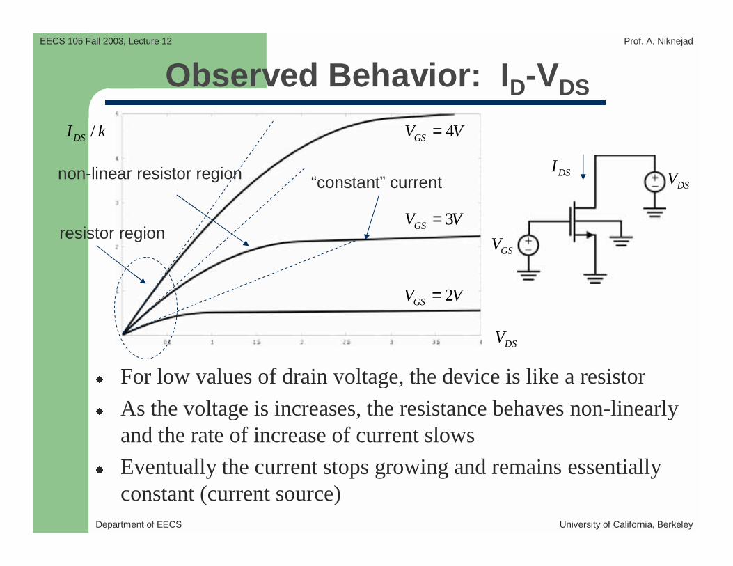
Observed Behavior: ID-VDS
� For low values of drain voltage, the device is like a resistor
� As the voltage is increases, the resistance behaves non-linearly and the rate of increase of current slows
� Eventually the current stops growing and remains essentially constant (current source)
DSV
/DSI k
“constant” current
resistor region
non-linear resistor region
2GSV V=
3GSV V=
4GSV V=
GSV
DSIDSV

Department of EECS University of California, Berkeley
EECS 105 Fall 2003, Lecture 12 Prof. A. Niknejad
“Linear” Region Current
� If the gate is biased above threshold, the surface is inverted
� This inverted region forms a channel that connects the drain and gate
� If a drain voltage is applied positive, electrons will flow from source to drain
p-type
n+ n+p+
Inversion layer“channel”
GS TnV V>
100mVDSV ≈G
DS
NMOS
x
y
Department of EECS University of California, Berkeley
EECS 105 Fall 2003, Lecture 12 Prof. A. Niknejad
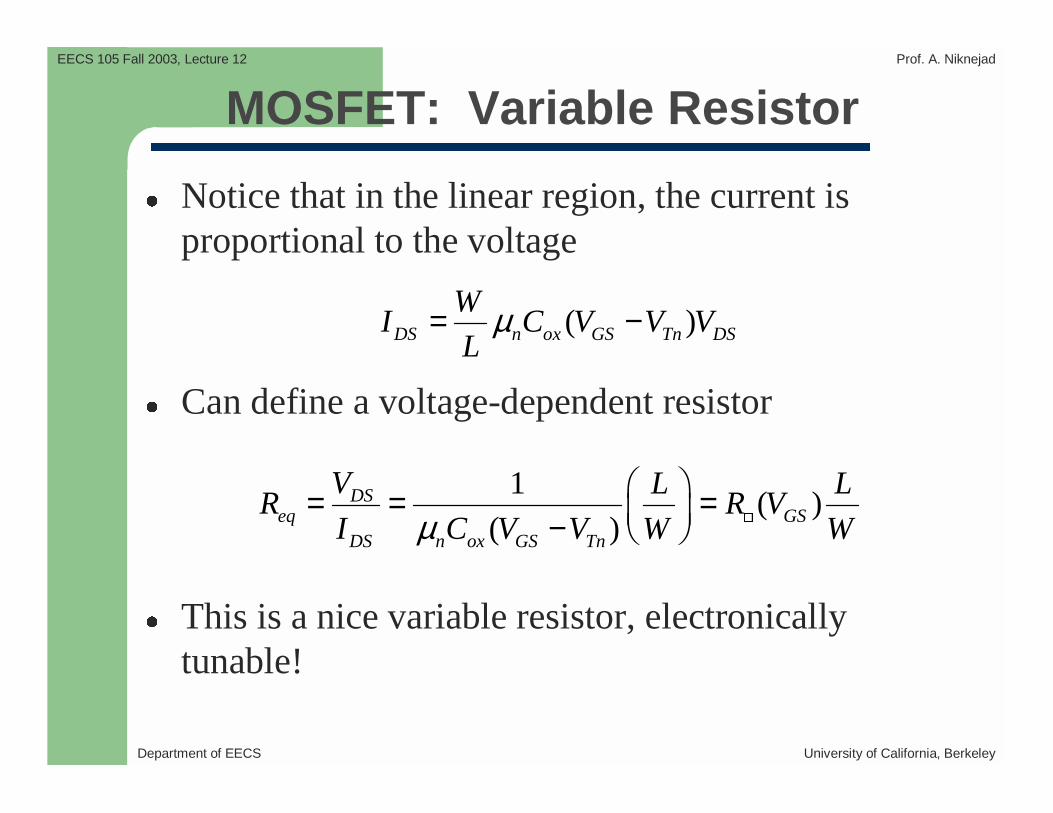
MOSFET: Variable Resistor
� Notice that in the linear region, the current is proportional to the voltage
� Can define a voltage-dependent resistor
� This is a nice variable resistor, electronically tunable!
( )DS n ox GS Tn DS
WI C V V V
Lµ= −
1( )
( )DS
eq GSDS n ox GS Tn
V L LR R V
I C V V W Wµ = = = −
�
Department of EECS University of California, Berkeley
EECS 105 Fall 2003, Lecture 12 Prof. A. Niknejad
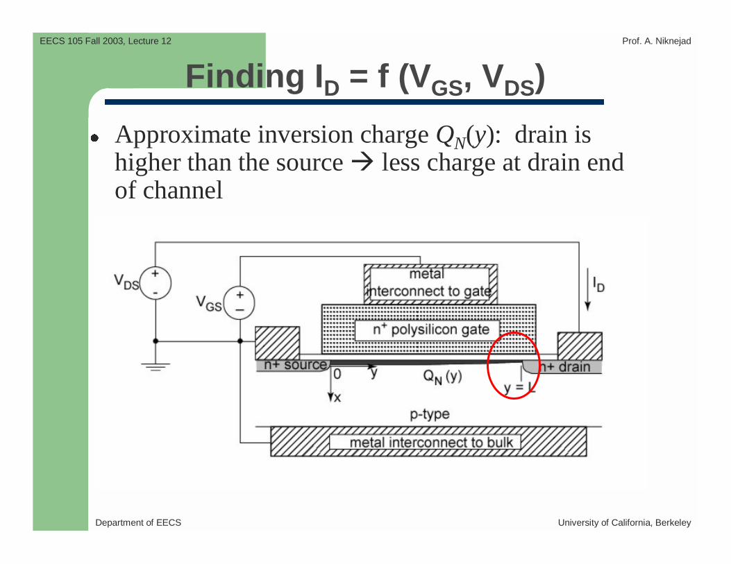
Finding ID = f (VGS, VDS)
� Approximate inversion charge QN(y): drain is higher than the source � less charge at drain end of channel

Department of EECS University of California, Berkeley
EECS 105 Fall 2003, Lecture 12 Prof. A. Niknejad
Inversion Charge at Source/Drain
)()0()( LyQyQyQ NNN =+=≈
)()0( TnGSoxN VVCyQ −−== == )( LyQN
)( TnGDox VVC −−
DSGSGD VV −=

Department of EECS University of California, Berkeley
EECS 105 Fall 2003, Lecture 12 Prof. A. Niknejad
Average Inversion Charge
� Charge at drain end is lower since field is lower
� Simple approximation: In reality we should integrate the total charge minus the bulk depletion charge across the channel
( ) ( )( )
2ox GS T ox GD T
N
C V V C V VQ y
− + −≈ −
Source End Drain End
( ) ( )( )
2ox GS T ox GS SD T
N
C V V C V V VQ y
− + − −≈ −
(2 2 )( ) ( )
2 2ox GS T ox SD DS
N ox GS T
C V V C V VQ y C V V
− −≈ − = − − −

Department of EECS University of California, Berkeley
EECS 105 Fall 2003, Lecture 12 Prof. A. Niknejad
Drift Velocity and Drain Current
“Long-channel” assumption: use mobility to find v
( ) ( ) ( / ) n DSn n
Vv y E y V y
L
µµ µ= − ≈ − −∆ ∆ =
Substituting:
( )2
DS DSD N ox GS T
V VI WvQ W C V V
Lµ= − ≈ − −
( )2DS
D ox GS T DS
VWI C V V V
Lµ≈ − −
Inverted Parabolas

Department of EECS University of California, Berkeley
EECS 105 Fall 2003, Lecture 12 Prof. A. Niknejad
Square-Law Characteristics
Boundary: what is ID,SAT?TRIODE REGION
SATURATION REGION

Department of EECS University of California, Berkeley
EECS 105 Fall 2003, Lecture 12 Prof. A. Niknejad
The Saturation Region
When VDS > VGS – VTn, there isn’t any inversioncharge at the drain … according to our simplistic model
Why do curvesflatten out?
Department of EECS University of California, Berkeley
EECS 105 Fall 2003, Lecture 12 Prof. A. Niknejad
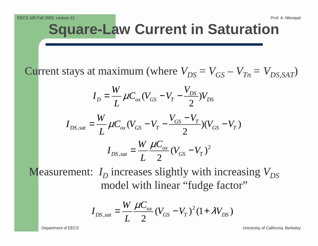
Square-Law Current in Saturation
Current stays at maximum (where VDS = VGS – VTn = VDS,SAT)
Measurement: ID increases slightly with increasing VDS
model with linear “fudge factor”
( )2DS
D ox GS T DS
VWI C V V V
Lµ= − −
, ( )( )2
GS TDS sat ox GS T GS T
V VWI C V V V V
Lµ −= − − −
2, ( )
2ox
DS sat GS T
CWI V V
L
µ= −
2, ( ) (1 )
2ox
DS sat GS T DS
CWI V V V
L
µ λ= − +

Department of EECS University of California, Berkeley
EECS 105 Fall 2003, Lecture 12 Prof. A. Niknejad
Pinching the MOS Transistors
� When VDS > VDS,sat, the channel is “pinched” off at drain end (hence the name “pinch-off region”)
� Drain mobile charge goes to zero (region is depleted), the remaining elecricfield is dropped across this high-field depletion region
� As the drain voltage is increases further, the pinch off point moves back towards source
� Channel Length Modulation: The effective channel length is thus reduced � higher IDS
p-type
n+ n+p+
Pinch-Off Point
GS TnV V>
DSVG
DS
NMOS
Depletion RegionGS TnV V−

Department of EECS University of California, Berkeley
EECS 105 Fall 2003, Lecture 12 Prof. A. Niknejad
Linear MOSFET Model
Channel (inversion) charge: neglect reduction at drain
Velocity saturation defines VDS,SAT = Esat L = constant
- vsat / µnDrain current:
)],()[(, TnGSoxsatNSATD VVCvWWvQI −−−=−=
|Esat| = 104 V/cm, L = 0.12 µm � VDS,SAT = 0.12 V!
)1)((, DSnTnGSoxsatSATD VVVWCvI λ+−=

Department of EECS University of California, Berkeley
EECS 105 Fall 2003, Lecture 12 Prof. A. Niknejad
Why Find an Incremental Model?
� Signals of interest in analog ICs are often of the form:
Direct substitution into iD = f(vGS, vDS) is tedious AND doesn’t include charge-storage effects … pretty rough approximation
( ) ( )GS GS gsv t V v t= +
Fixed Bias Point Small Signal

Department of EECS University of California, Berkeley
EECS 105 Fall 2003, Lecture 12 Prof. A. Niknejad
Which Operating Region?
3VGSV =
3VDSV =TRIODE
SAT
OFF

Department of EECS University of California, Berkeley
EECS 105 Fall 2003, Lecture 12 Prof. A. Niknejad
Changing One Variable at a Time
Assumption: VDS > VDS,SAT = VGS – VTn (square law)
GSV
/DSI k
3VDSV =1VTV =
Square LawSaturation
Region
Linear TriodeRegion
Slope of Tangent: Incremental current increase

Department of EECS University of California, Berkeley
EECS 105 Fall 2003, Lecture 12 Prof. A. Niknejad
The Transconductance gm
Defined as the change in drain current due to a change in the gate-source voltage, with everything else constant
, ,
( )(1 )GS DS GS DS
D Dm ox GS T DS
GS GSV V V V
i i Wg C V V V
v v Lµ λ∆ ∂= = = − +
∆ ∂
2, ( ) (1 )
2ox
DS sat GS T DS
CWI V V V
L
µ λ= − +
( )m ox GS T
Wg C V V
Lµ= −
0≈
22DS
m ox ox DS
ox
IW Wg C C I
WL LCL
µ µµ
= =
2
( )DS
mGS T
Ig
V V=
−
Gate Bias
Drain Current Bias
Drain Current Bias and Gate Bias

Department of EECS University of California, Berkeley
EECS 105 Fall 2003, Lecture 12 Prof. A. Niknejad
Output Resistance ro
Defined as the inverse of the change in drain current dueto a change in the drain-source voltage, with everythingelse constant
Non-Zero Slope
DSVδ
DSIδ

Department of EECS University of California, Berkeley
EECS 105 Fall 2003, Lecture 12 Prof. A. Niknejad
Evaluating ro
1
,GS DS
Do
DS V V
ir
v
− ∂ = ∂
2( ) (1 )2
oxD GS T DS
CWi V V V
L
µ λ= − +
02
1
( )2
oxGS T
rCW
V VL
µ λ=
−
0
1
DS
rIλ
≈

Department of EECS University of California, Berkeley
EECS 105 Fall 2003, Lecture 12 Prof. A. Niknejad
Total Small Signal Current
( )DS DS dsi t I i= +
DS DSds gs ds
gs ds
i ii v v
v v
∂ ∂= +∂ ∂
1ds m gs ds
o
i g v vr
= +
TransconductanceConductance
Department of EECS University of California, Berkeley
EECS 105 Fall 2003, Lecture 12 Prof. A. Niknejad
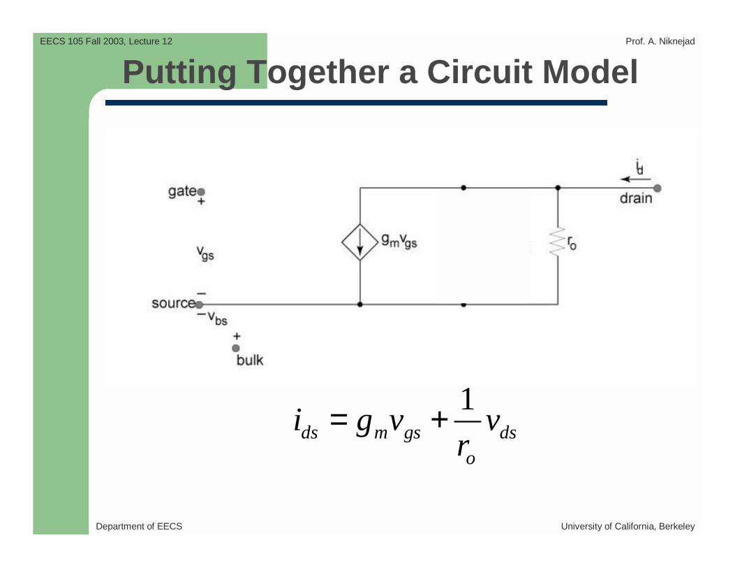
Putting Together a Circuit Model
1ds m gs ds
o
i g v vr
= +

Department of EECS University of California, Berkeley
EECS 105 Fall 2003, Lecture 12 Prof. A. Niknejad
Role of the Substrate Potential
Need not be the source potential, but VB < VS
Effect: changes threshold voltage, which changes the drain current … substrate acts like a “backgate”
QBS
D
QBS
Dmb v
i
v
ig
∂∂=
∆∆=
Q = (VGS, VDS, VBS)

Department of EECS University of California, Berkeley
EECS 105 Fall 2003, Lecture 12 Prof. A. Niknejad
Backgate Transconductance
Result:2 2
Tn mD Dmb
BS Tn BS BS pQ Q Q
V gi ig
v V v V
γφ
∂∂ ∂= = =∂ ∂ ∂ − −
( )0 2 2T T SB p pV V Vγ φ φ= + − − −

Department of EECS University of California, Berkeley
EECS 105 Fall 2003, Lecture 12 Prof. A. Niknejad
Four-Terminal Small-Signal Model
1ds m gs mb bs ds
o
i g v g v vr
= + +
Department of EECS University of California, Berkeley
EECS 105 Fall 2003, Lecture 12 Prof. A. Niknejad
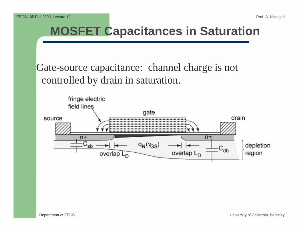
MOSFET Capacitances in Saturation
Gate-source capacitance: channel charge is not controlled by drain in saturation.

Department of EECS University of California, Berkeley
EECS 105 Fall 2003, Lecture 12 Prof. A. Niknejad
Gate-Source Capacitance Cgs
Wedge-shaped charge in saturation � effective area is (2/3)WL(see H&S 4.5.4 for details)
ovoxgs CWLCC += )3/2(
Overlap capacitance along source edge of gate �
oxDov WCLC =
(Underestimate due to fringing fields)

Department of EECS University of California, Berkeley
EECS 105 Fall 2003, Lecture 12 Prof. A. Niknejad
Gate-Drain Capacitance Cgd
Not due to change in inversion charge in channel
Overlap capacitance Cov between drain and sourceis Cgd

Department of EECS University of California, Berkeley
EECS 105 Fall 2003, Lecture 12 Prof. A. Niknejad
Junction Capacitances
Drain and source diffusions have (different) junctioncapacitances since VSB and VDB = VSB + VDS aren’t the same
Complete model (without interconnects)

Department of EECS University of California, Berkeley
EECS 105 Fall 2003, Lecture 12 Prof. A. Niknejad
P-Channel MOSFET
Measurement of –IDp versus VSD, with VSG as a parameter:

Department of EECS University of California, Berkeley
EECS 105 Fall 2003, Lecture 12 Prof. A. Niknejad
Square-Law PMOS Characteristics

Department of EECS University of California, Berkeley
EECS 105 Fall 2003, Lecture 12 Prof. A. Niknejad
Small-Signal PMOS Model
Department of EECS University of California, Berkeley
EECS 105 Fall 2003, Lecture 12 Prof. A. Niknejad
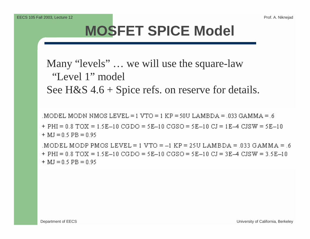
MOSFET SPICE Model
Many “levels” … we will use the square-law “Level 1” model
See H&S 4.6 + Spice refs. on reserve for details.