Embed Size (px)
Citation preview
Power Electronics Lab 1
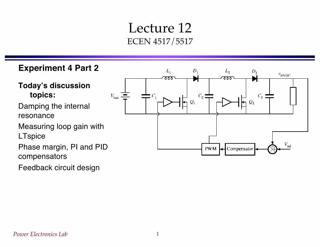
Lecture 12ECEN 4517/5517
Experiment 4 Part 2
Today’s discussion topics:
Damping the internal resonanceMeasuring loop gain with LTspicePhase margin, PI and PID compensatorsFeedback circuit design
Power Electronics Lab 2
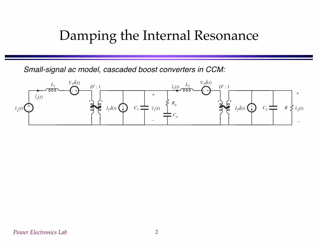
Damping the Internal Resonance
+–
L1+–
V1F(t)
I1F(t)
K1(t)
Xg(t)
De : 1 L2
C2 R
+–
V2F(t)
I2F(t)
K2(t)+
–
X2(t)
De : 1
C1
+
–
X1(t)Cd
Rd
Small-signal ac model, cascaded boost converters in CCM:
Power Electronics Lab 10
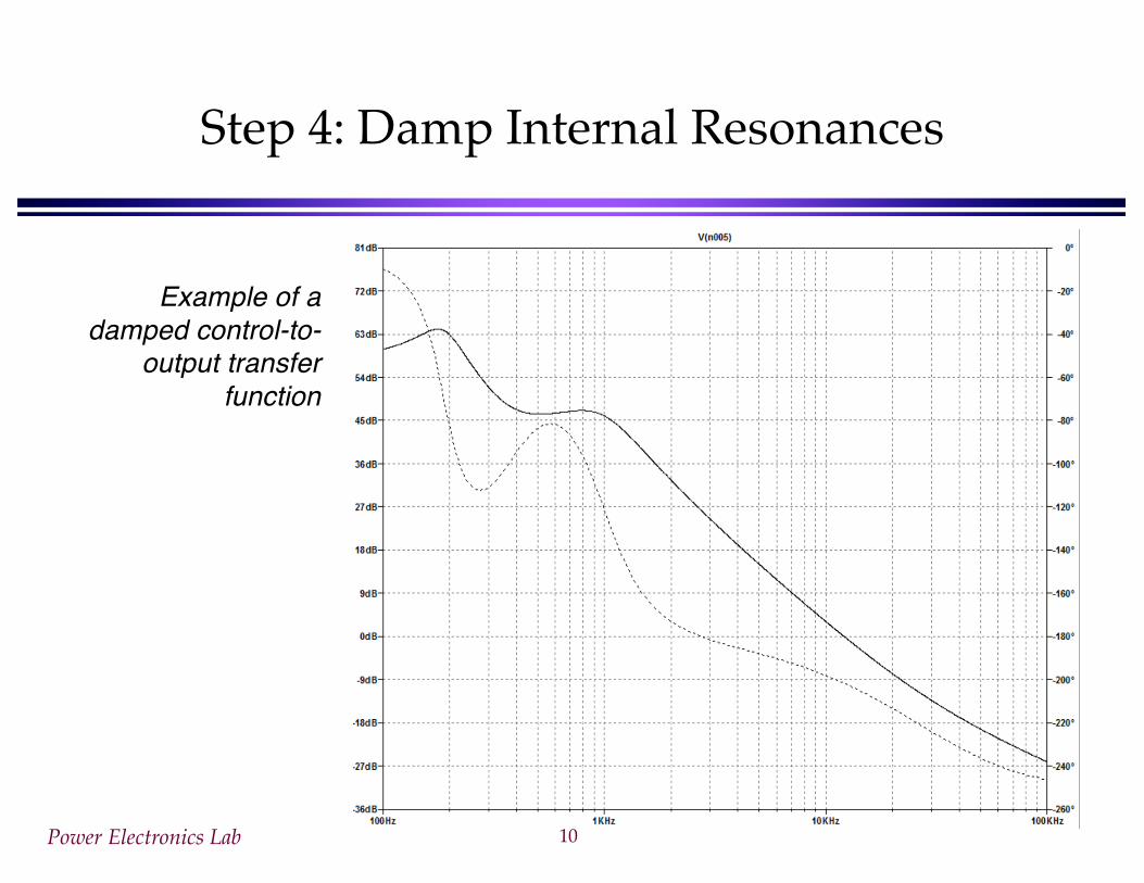
Step 4: Damp Internal Resonances
Example of a damped control-to-
output transfer function
Fundamentals of Power Electronics Chapter 9: Controller design64
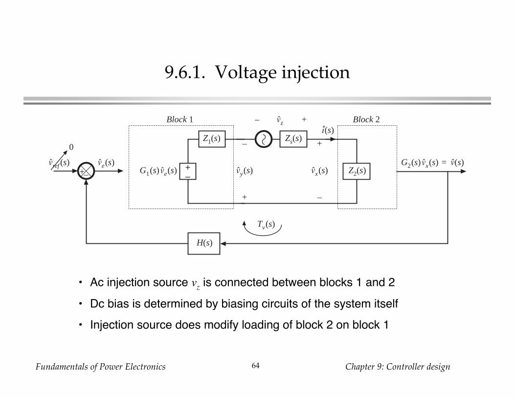
9.6.1. Voltage injection
• Ac injection source vz is connected between blocks 1 and 2• Dc bias is determined by biasing circuits of the system itself• Injection source does modify loading of block 2 on block 1
+–
H(s)
+–
Z2(s)
Block 1 Block 2
0
Tv(s)
Z1(s) Zs(s)
– +
+
vx(s)
–
vref (s)G1(s)ve(s)
ve(s) G2(s)vx(s) = v(s)
–
vy(s)
+
vzi(s)
Power Electronics Lab 14
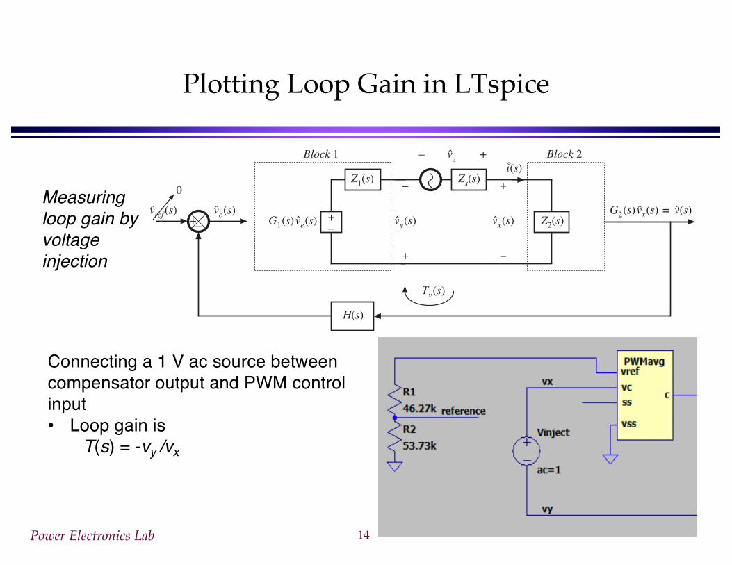
Plotting Loop Gain in LTspice
+–
H(s)
+– Z2(s)
Block 1 Block 2
0
Tv(s)
Z1(s) Zs(s)
– +
+
vx(s)
–
vref (s)G1(s)ve(s)
ve(s) G2(s)vx(s) = v(s)
–
vy(s)
+
vzi(s)
Measuring loop gain by voltage injection
Connecting a 1 V ac source between compensator output and PWM control input• Loop gain is
T(s) = -vy /vx
Power Electronics Lab 15
Convergence Problems
• In closed-loop simulations, LTspice often encounters convergence problems and cannot find quiescent operating point
• A solution: provide initial conditions for a few key capacitor voltages and/or inductor currents• Append “IC=value” to element value• Set initial conditions on output capacitor voltage and compensator integrator
capacitor voltage to their correct steady-state values• Setting initial conditions on the above may be sufficient to get the closed-
loop simulation to run
Fundamentals of Power Electronics Chapter 9: Controller design25
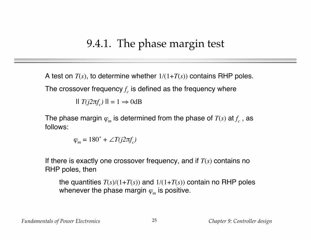
9.4.1. The phase margin test
A test on T(s), to determine whether 1/(1+T(s)) contains RHP poles.
The crossover frequency fc is defined as the frequency where
|| T(j2πfc) || = 1 ⇒ 0dB
The phase margin ϕm is determined from the phase of T(s) at fc , asfollows:
ϕm = 180˚ + ∠T(j2πfc)
If there is exactly one crossover frequency, and if T(s) contains noRHP poles, then
the quantities T(s)/(1+T(s)) and 1/(1+T(s)) contain no RHP poleswhenever the phase margin ϕm is positive.
Fundamentals of Power Electronics Chapter 9: Controller design38
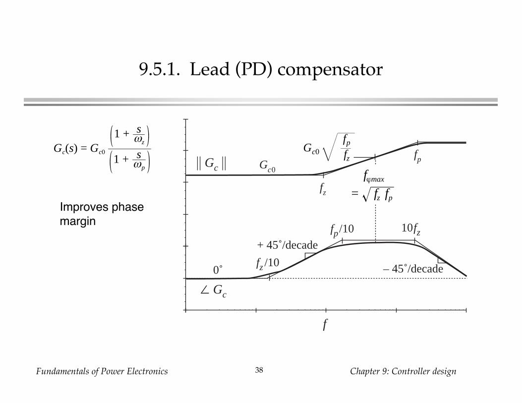
9.5.1. Lead (PD) compensator
Gc(s) = Gc0
1 + sωz
1 + sωp
Improves phasemargin
f
|| Gc ||
∠ Gc
Gc0
0˚
fp
fz /10
fp/10 10fz
fϕmax
= fz fp
+ 45˚/decade
– 45˚/decade
fz
Gc0
fp
fz
Fundamentals of Power Electronics Chapter 9: Controller design39
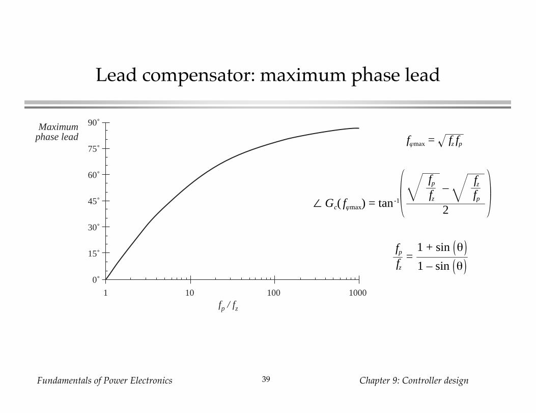
Lead compensator: maximum phase lead
fϕmax = fz fp
∠ Gc( fϕmax) = tan-1
fp
fz–
fzfp
2
fp
fz=
1 + sin θ
1 – sin θ
1 10 100 1000
Maximumphase lead
0˚
15˚
30˚
45˚
60˚
75˚
90˚
fp / fz
Fundamentals of Power Electronics Chapter 9: Controller design40
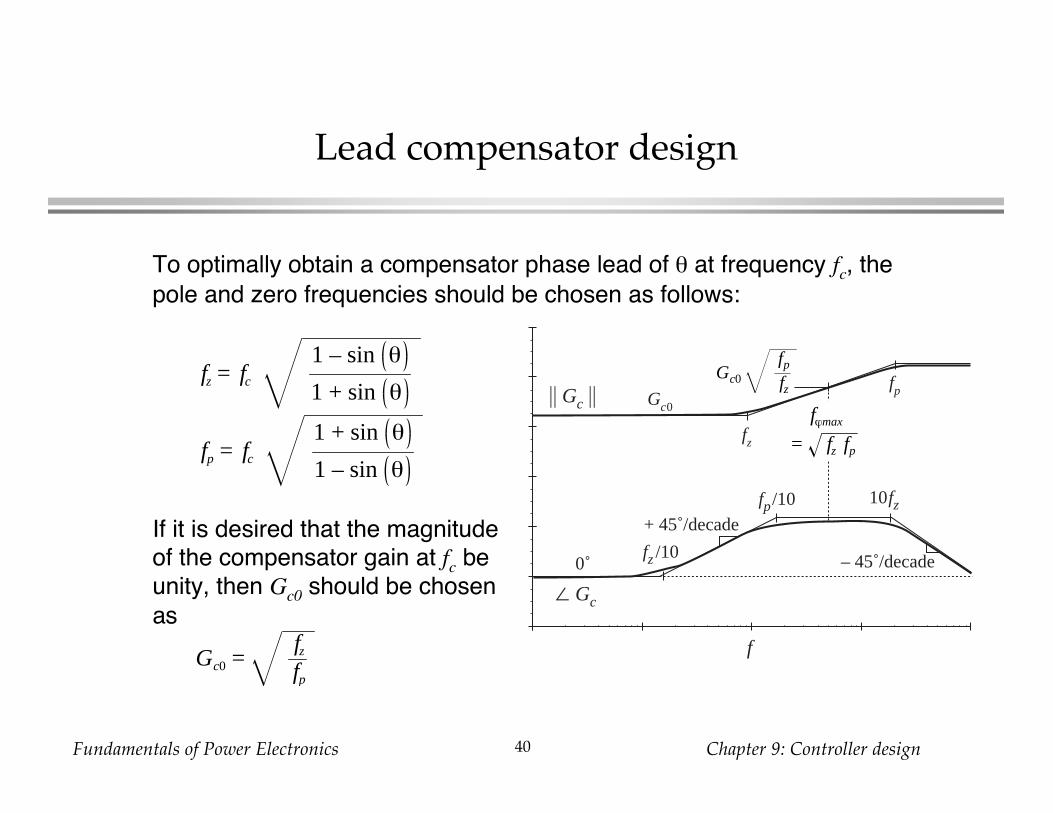
Lead compensator design
To optimally obtain a compensator phase lead of θ at frequency fc, thepole and zero frequencies should be chosen as follows:
fz = fc1 – sin θ
1 + sin θ
fp = fc1 + sin θ
1 – sin θ
If it is desired that the magnitudeof the compensator gain at fc beunity, then Gc0 should be chosenas
Gc0 =fzfp
f
|| Gc ||
∠ Gc
Gc0
0˚
fp
fz /10
fp/10 10fz
fϕmax
= fz fp
+ 45˚/decade
– 45˚/decade
fz
Gc0
fp
fz
Fundamentals of Power Electronics Chapter 9: Controller design41
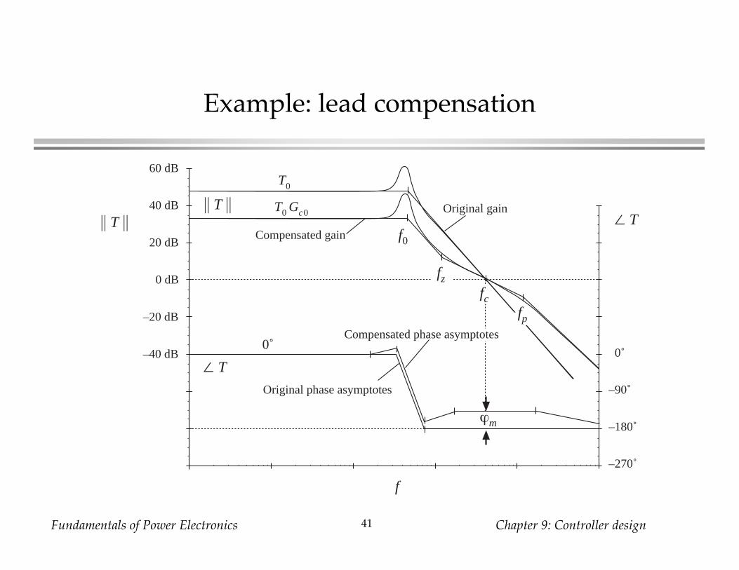
Example: lead compensation
f
|| T ||
0˚
–90˚
–180˚
–270˚
∠ T
|| T || ∠ T
T0
f0
0˚
fzfc
ϕm
T0 Gc0 Original gain
Compensated gain
Original phase asymptotes
Compensated phase asymptotes
0 dB
–20 dB
–40 dB
20 dB
40 dB
60 dB
fp
Fundamentals of Power Electronics Chapter 9: Controller design42
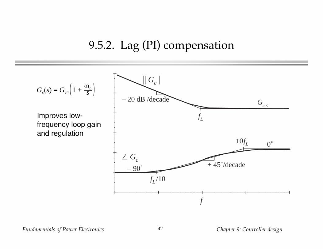
9.5.2. Lag (PI) compensation
Gc(s) = Gc∞ 1 +ωLs
Improves low-frequency loop gainand regulation
f
|| Gc ||
∠ Gc
Gc∞
0˚
fL/10
+ 45˚/decade
fL
– 90˚
10fL
– 20 dB /decade
Fundamentals of Power Electronics Chapter 9: Controller design43
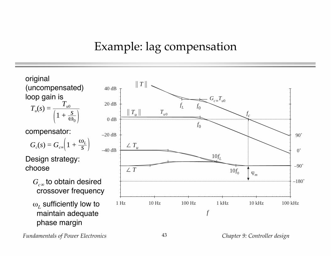
Example: lag compensation
original(uncompensated)loop gain is
Tu(s) =Tu0
1 + sω0
compensator:Gc(s) = Gc∞ 1 +
ωLs
Design strategy:choose
Gc∞ to obtain desiredcrossover frequencyωL sufficiently low tomaintain adequatephase margin
0 dB
–20 dB
–40 dB
20 dB
40 dB
f
90˚
0˚
–90˚
–180˚
Gc∞Tu0fL
f0
Tu0
∠ Tu
|| Tu ||f0
|| T ||
fc
∠ T
10fL
10f0 ϕm
1 Hz 10 Hz 100 Hz 1 kHz 10 kHz 100 kHz
Fundamentals of Power Electronics Chapter 9: Controller design45
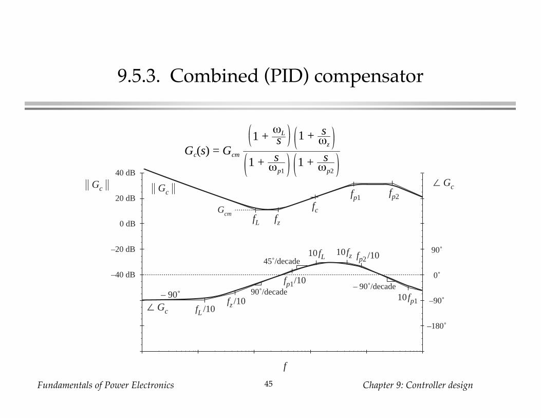
9.5.3. Combined (PID) compensator
Gc(s) = Gcm
1 +ωLs 1 + s
ωz
1 + sωp1
1 + sωp2
0 dB
–20 dB
–40 dB
20 dB
40 dB
f
|| Gc ||
∠ Gc
|| Gc || ∠ Gc
Gcmfz
– 90˚
fp1
90˚
0˚
–90˚
–180˚
fz /10
fp1/10
10 fz
fL
fc
fL /10
10 fL
90˚/decade
45˚/decade
– 90˚/decade
fp2
fp2 /10
10 fp1
Power Electronics Lab 11
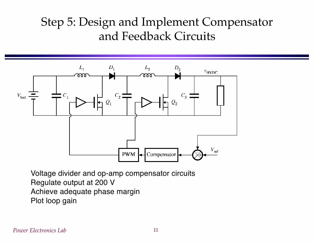
Step 5: Design and Implement Compensator and Feedback Circuits
Voltage divider and op-amp compensator circuitsRegulate output at 200 VAchieve adequate phase marginPlot loop gain
Power Electronics Lab 12
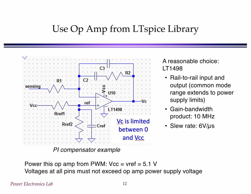
Use Op Amp from LTspice Library
A reasonable choice: LT1498• Rail-to-rail input and
output (common mode range extends to power supply limits)
• Gain-bandwidth product: 10 MHz
• Slew rate: 6V/µs
Power this op amp from PWM: Vcc = vref = 5.1 VVoltages at all pins must not exceed op amp power supply voltage
PI compensator example
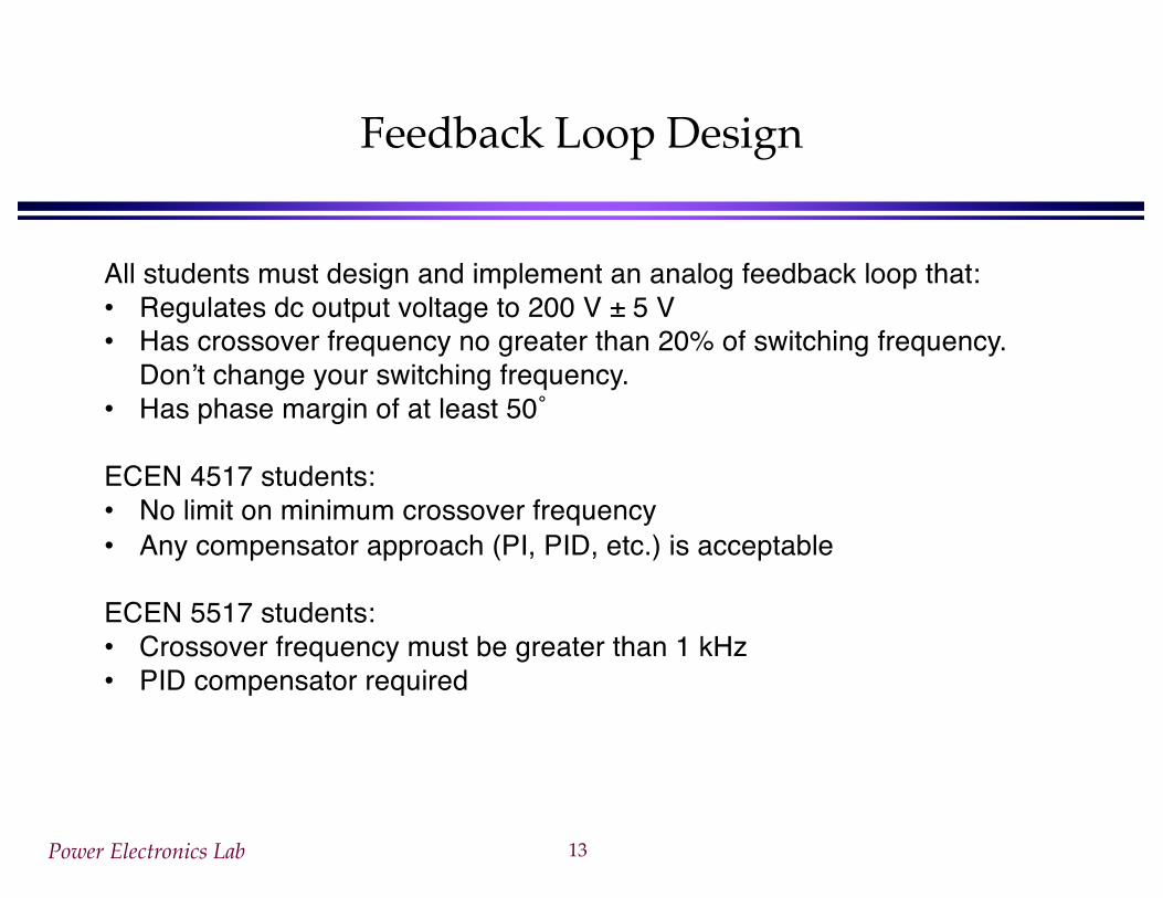
Power Electronics Lab 13
Feedback Loop Design
All students must design and implement an analog feedback loop that:• Regulates dc output voltage to 200 V ± 5 V• Has crossover frequency no greater than 20% of switching frequency.
Don’t change your switching frequency.• Has phase margin of at least 50˚
ECEN 4517 students:• No limit on minimum crossover frequency• Any compensator approach (PI, PID, etc.) is acceptable
ECEN 5517 students:• Crossover frequency must be greater than 1 kHz• PID compensator required