Embed Size (px)
Citation preview
I. ELECTRONICS MODULEBY SAM KINYERA OBWOYA KYAMBOGO UNIVERSITY UGANDA
II. Prerequisite Courses or KnowledgeThe basic prerequisites for this module are the school physics that one has learnt. In particular, knowledge of the following courses are essential for one to follow and understand the module effectively. Some of the prerequisite courses are solids state physics, electricity and magnetism. As a general requirement, you need the knowledge of calculus and algebra in mathematics.
III. TimeA total of 120 hours is required for you to complete this module.
IV. MaterialThe materials required for the module include access to a computer, but more importantly one needs a steady access to internet. The internet will provide many of the essential references and multimedia resources. These multimedia are important as in some cases they serve as virtual lecturers and sources of equipment that can be used to perform virtual experiments. However, some CD-ROMS will also be available to supplement the use of internet. Other materials include compulsory readings and compulsory resources that may be available at nearby bookshops or schools.
V. Module RationaleThis module is intended to provide a basic foundation of physics to students. This will enable the students to learn the subject matter in order to explain and account for the principles involved in electronics. The module is structured such that the learner has to go through the activities as prescribed for maximum attainment. The overall module will provide the student with basic ideas of what electronics is in terms of the key components’ behaviours or characteristics and therefore will be enable to teach most of the school physics effectively.
VI. OverviewElectronics is the study of the flow of charge through various materials and devices such as, semiconductors, resistors, inductors, capacitors, nano-structures, and vacuum tubes. All applications of electronics involve the transmission of power and possibly information. Although considered to be a theoretical branch of physics, the design and construction of electronic circuits to solve practical problems is an essential technique in the fields of electronic engineering and computer engineering.
The study of new semiconductor devices and surrounding technology is sometimes considered a branch of physics. This module focuses on engineering aspects of electronics. Other important topics include electronic waste and occupational health impacts of semiconductor manufacturing.
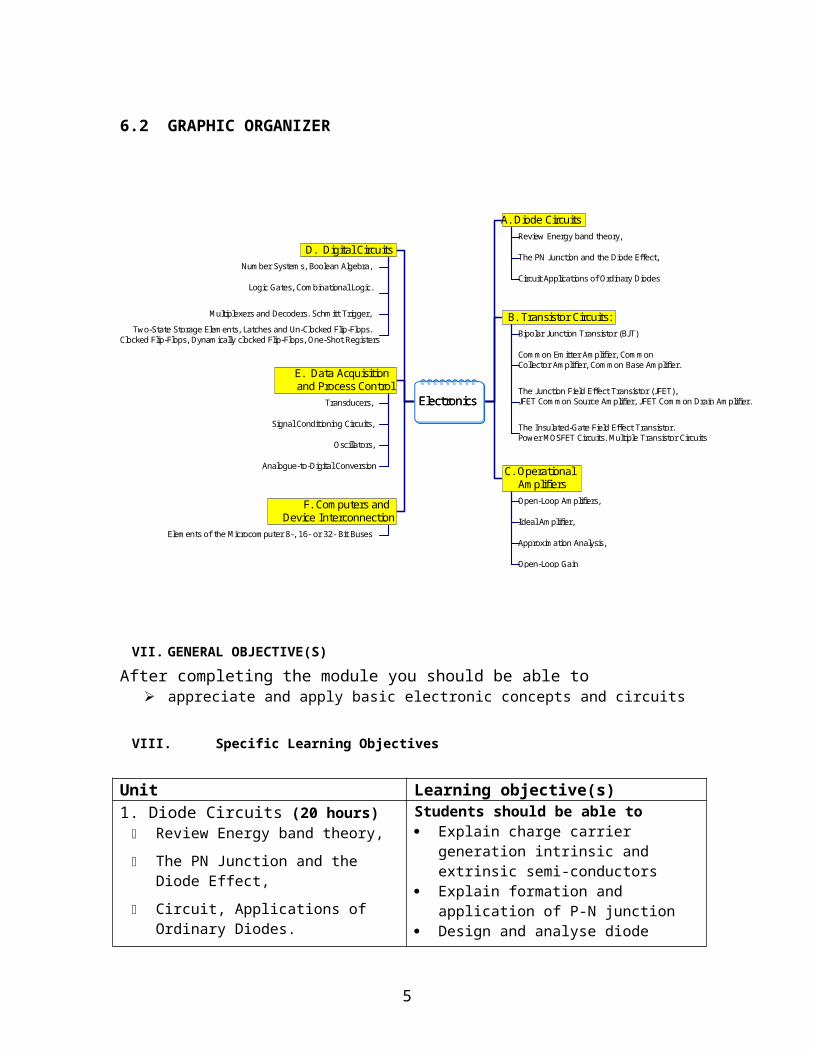
This course of electronics is intended for students enrolling for pre-service and in-service students registering for BSc with Education and BEd degrees. As you may be aware, Electronics forms one the back bone of modern physics. The module has six units: Diode Circuits; Transistor Circuits; Operational Amplifiers;
1
Digital Circuits; Data acquisition and Process Control; and Computers and Device Interconnection.
In the first unit/activity i.e. diodes circuits, students are expected to explain charge carrier generation, intrinsic and extrinsic semi-conductors, formation and application of P-N junction, and to design and analyse diode circuits (e.g, power supply circuits).
In the second unit/activity i.e. Transistor circuits, the student is expected to explain how a Bipolar Junction Transistor (BJT) works; Design and analyse basic BJT circuits in various configurations (CE, EB, CB); Explain how a junction Field Effect Transistor (JFET) works ; Design and analyse JFET circuits in both configurations (CD, CS); Explain how MOSFET works and also be able to Design and analyse MOSFET circuits.
In unit three the learning outcomes include one being able to explain the construction of operational amplifier; and to Design, analyse and synthesize operational amplifier circuits. In unit four, i.e. Digital Circuits, the student is expected to Manipulate numbers in various bases (2,8,10,16); Apply Boollean algebra in design of logic circuits; Design, analyse and synthesize logic circuits (multiplexer, decoders, Schmitt triggers, flip-flops, registers). In unit five the learner will explain the operation of a transducer in various modes (strain, light, piezo, temp); Explain and apply transducer signal conditioning processes; and to Apply conditioned signal in digital form. Finally, in activity six, i.e. Elements of the Microcomputer 8-, 16- or 32Bit buses, the expected learning will include explaining the systems level components of a microprocessor.
6.1 OUTLINE
Activity 1: Diode Circuits Review Energy band theory, The PN Junction and the Diode Effect, Circuit, Applications of Ordinary Diodes (20 hours)
Activity 2: Transistor Circuits Bipolar Junction Transistor (BJT) Common Emitter Amplifier, Common Collector Amplifier, Common Base Amplifier. The Junction Field Effect Transistor (JFET), JFET Common Source Amplifier, JFET Common Drain Amplifier. The Insulated-Gate Field Effect Transistor. Power MOSFET Circuits. Multiple Transistor Circuits (30 hours)
Activity 3: Operational Amplifiers Open-Loop Amplifiers, Ideal Amplifier, Approximation Analysis, Open-Loop Gain (10 hours)
Activity 4: Digital Circuits Number Systems, Boolean Algebra, Logic Gates, Combinational Logic. Multiplexers and Decoders. Schmitt Trigger, Two-State Storage Elements, Latches and Un-Clocked Flip-Flops. Clocked Flip-Flops, Dynamically clocked Flip-Flops, One-Shot Registers (30 hours)
Activity 5: Data Acquisition and Process Control Transducers, Signal Conditioning Circuits, Oscillators, Analogue-to-Digital Conversion (20 hours)
Activity 6: Computers and Device Interconnection Elements of the Microcomputer 8-, 16- or 32- Bit Buses (10 hours)
2
6.2 GRAPHIC ORGANIZER
VII. GENERAL OBJECTIVE(S)After completing the module you should be able to
appreciate and apply basic electronic concepts and circuits
VIII. Specific Learning Objectives
Unit Learning objective(s)1. Diode Circuits (20 hours)
Review Energy band theory,
The PN Junction and the Diode Effect,
Circuit, Applications of Ordinary Diodes.
Students should be able to Explain charge carrier generation
intrinsic and extrinsic semi-conductors Explain formation and application of P-
N junction Design and analyse diode circuits (e.g,
power supply circuits)
2. Transistor Circuits: (25 hours) Bipolar junction Transistor
Students should be able to Explain how a Bipolar Junction
Transistor (BJT) works
3
Electronics
A. Diode Circuits
B. Transistor Circuits:
C. OperationalAmplifiers
D. Digital Circuits
E. Data Acquisitionand Process Control
F. Computers andDevice Interconnection
Review Energy band theory,
The PN Junction and the Diode Effect,
Circuit Applications of Ordinary Diodes
Bipolar Junction Transistor (BJT)
Common Emitter Amplifier, CommonCollector Amplifier, Common Base Amplifier.
The Junction Field Effect Transistor (JFET),JFET Common Source Amplifier, JFET Common Drain Amplifier.
The Insulated-Gate Field Effect Transistor.Power MOSFET Circuits. Multiple Transistor Circuits
Open-Loop Amplifiers,
Ideal Amplifier,
Approximation Analysis,
Open-Loop Gain
Number Systems, Boolean Algebra,
Logic Gates, Combinational Logic.
Multiplexers and Decoders. Schmitt Trigger,Two-State Storage Elements, Latches and Un-Clocked Flip-Flops.
Clocked Flip-Flops, Dynamically clocked Flip-Flops, One-Shot Registers
Transducers,
Signal Conditioning Circuits,
Oscillators,
Analogue-to-Digital Conversion
Elements of the Microcomputer 8-, 16- or 32- Bit Buses
Electronics

(BJT);Common Emitter Amplifier; Common Collector Amplifier, Common Base Amplifier.
The Junction Field Effect Transistor (JFET), JFET Common Source Amplifier, JFET Common Drain amplifier.
The Insulated-Gate Field Effect Transistor. Power
MOSFET Circuits, Multiple Transistor Circuit
Design and analyse basic BJT circuits in various configurations (CE, EB, CB)
Explain how a junction Field Effect Transistor (JFET) works (some theory)
Design and analyse JFET circuits in both configurations (CD, CS)
Explain how MOSFET works (theory) Design and analyse MOSFET circuits
3. Operational Amplifiers (10 hours) Open loop Amplifiers,
Ideal Amplifiers, Apporoximation Analysis, Ope-loop Gain.
Students should be able to Explain the construction of operational
amplifier Design, analyse and synthesize
operational amplifier circuits
4. Digital Circuits (30 hours) Number systems, Boolean Algebra,
Logic Gates,
Combinational Logic,
Multiplexes and decoders, Schmitt Trigger, Two-State storage elements,
Latches and un-clocked flip-flops;
Dynamically clocked flipiflops,
One-shot registers
Students should be able to Manipulate numbers in various bases
(2,8,10,16) Apply Boollean algebra in design of
logic circuits Design, analyse and synthesize logic
circuits (multiplexer, decoders, Smchmitt triggers, flip-flops, registers)
5. Data acquisition and Process Control (20 hours)
Transducers, Signal Conditioning
circuits, Oscillators, Analogue-to-Digital Conversion
Students should be able to Explain the operation of a transducer in
various modes (strain, light, piezo, temp)
Explain and apply transducer signal conditioning processes
Apply conditioned signal in digital form6. Computers and Device Interconnection
(15 hours) Elements of the Microcomputer 8-,
16- or 32- Bit Buses
Explain the systems level components of a microprocessor
4
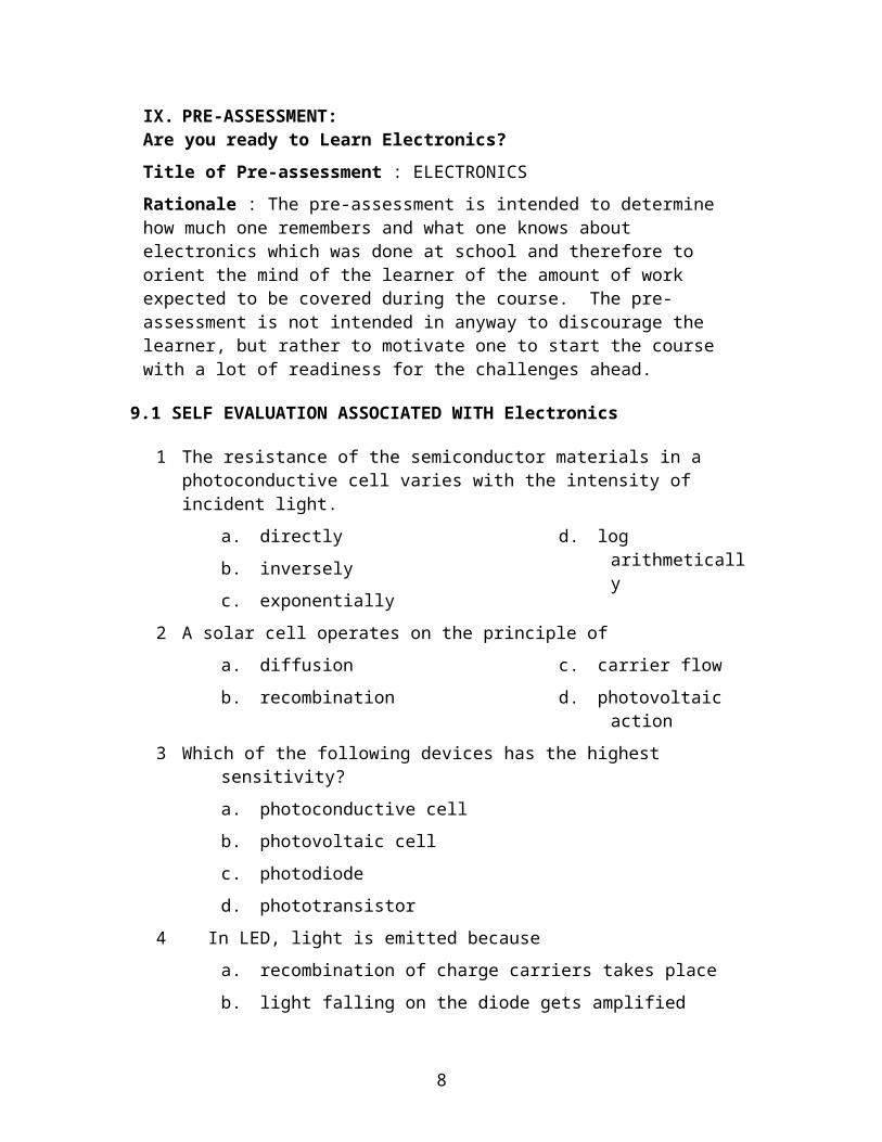
IX. PRE-ASSESSMENT: Are you ready to Learn Electronics?Title of Pre-assessment : ELECTRONICS
Rationale : The pre-assessment is intended to determine how much one remembers and what one knows about electronics which was done at school and therefore to orient the mind of the learner of the amount of work expected to be covered during the course. The pre-assessment is not intended in anyway to discourage the learner, but rather to motivate one to start the course with a lot of readiness for the challenges ahead.
9.1 SELF EVALUATION ASSOCIATED WITH Electronics
1 The resistance of the semiconductor materials in a photoconductive cell varies with the intensity of incident light.
a. directly
b. inversely
c. exponentially
d. log arithmetically
2 A solar cell operates on the principle of
a. diffusion
b. recombination
c. carrier flow
d. photovoltaic action
3 Which of the following devices has the highest sensitivity?
a. photoconductive cell
b. photovoltaic cell
c. photodiode
d. phototransistor
4 In LED, light is emitted because
a. recombination of charge carriers takes place
b. light falling on the diode gets amplified
c. light gets reflected due to lens action
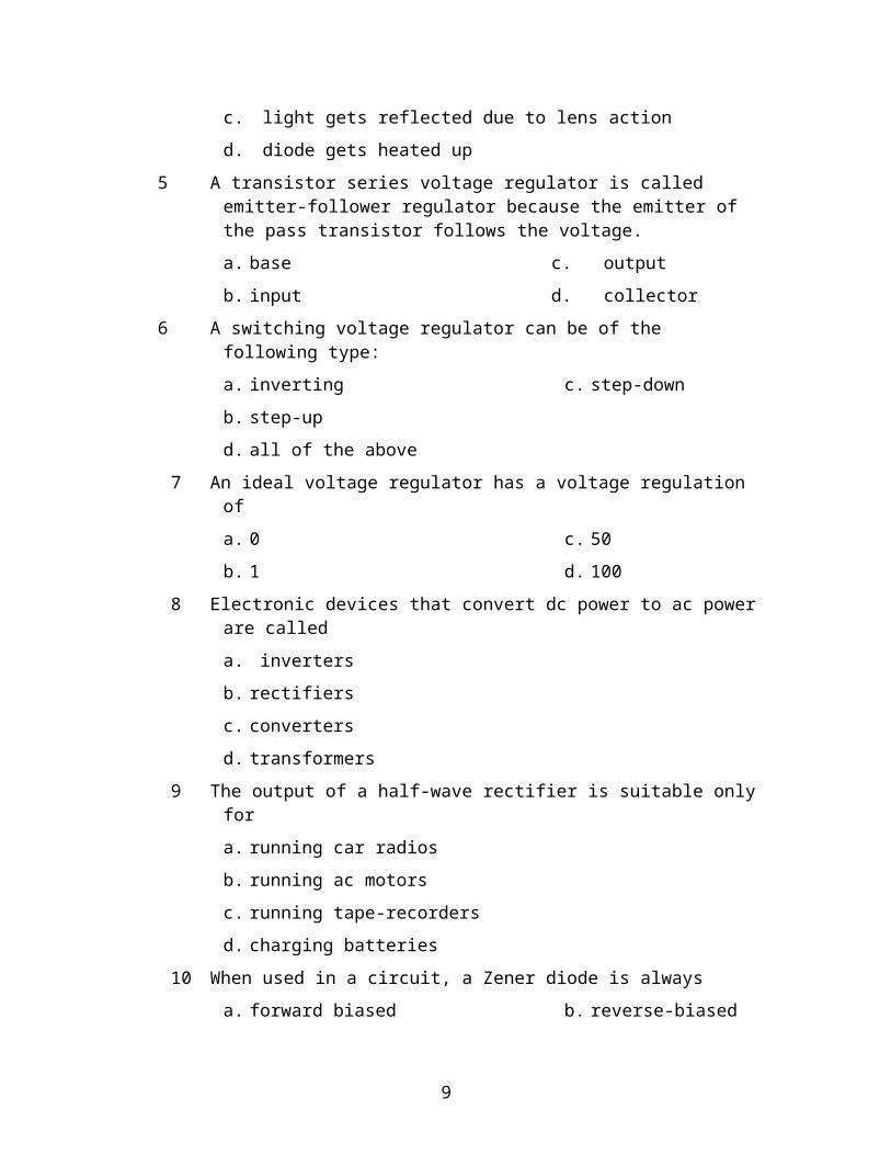
d. diode gets heated up
5 A transistor series voltage regulator is called emitter-follower regulator because the emitter of the pass transistor follows the voltage.
a. base
b. input
c. output
d. collector
6 A switching voltage regulator can be of the following type:
a. inverting
b. step-up
c. step-down
5
d. all of the above
7 An ideal voltage regulator has a voltage regulation of
a. 0
b. 1
c. 50
d. 100
8 Electronic devices that convert dc power to ac power are called
a. inverters
b. rectifiers
c. converters
d. transformers
9 The output of a half-wave rectifier is suitable only for
a. running car radios
b. running ac motors
c. running tape-recorders
d. charging batteries
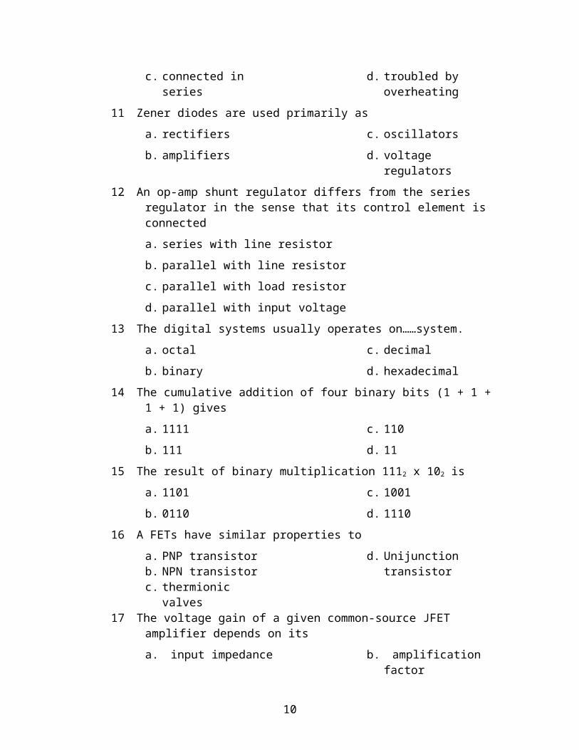
10 When used in a circuit, a Zener diode is always
a. forward biased
b. reverse-biased
c. connected in series
d. troubled by overheating
11 Zener diodes are used primarily as
a. rectifiers
b. amplifiers
c. oscillators
d. voltage regulators
12 An op-amp shunt regulator differs from the series regulator in the sense that its control element is connected
a. series with line resistor
b. parallel with line resistor
c. parallel with load resistor
d. parallel with input voltage
13 The digital systems usually operates on……system.
a. octal
b. binary
c. decimal
d. hexadecimal
14 The cumulative addition of four binary bits (1 + 1 + 1 + 1) gives
a. 1111
b. 111
c. 110
d. 11
6
15 The result of binary multiplication 1112 x 102 isa. 1101
b. 0110
c. 1001
d. 1110
16 A FETs have similar properties to
a. PNP transistorb. NPN transistor
c. thermionic valvesd. Unijunction transistor
17 The voltage gain of a given common-source JFET amplifier depends on its
a. input impedance
b. amplification factor
c. dynamic drain resistance
d. drain load resistance
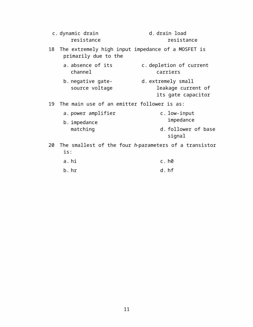
18 The extremely high input impedance of a MOSFET is primarily due to the
a. absence of its channel
b. negative gate-source voltage
c. depletion of current carriers
d. extremely small leakage current of its gate capacitor
19 The main use of an emitter follower is as:
a. power amplifier
b. impedance matching
c. low-input impedance
d. follower of base signal
20 The smallest of the four h-parameters of a transistor is:
a. hi
b. hr
c. h0
d. hf
7
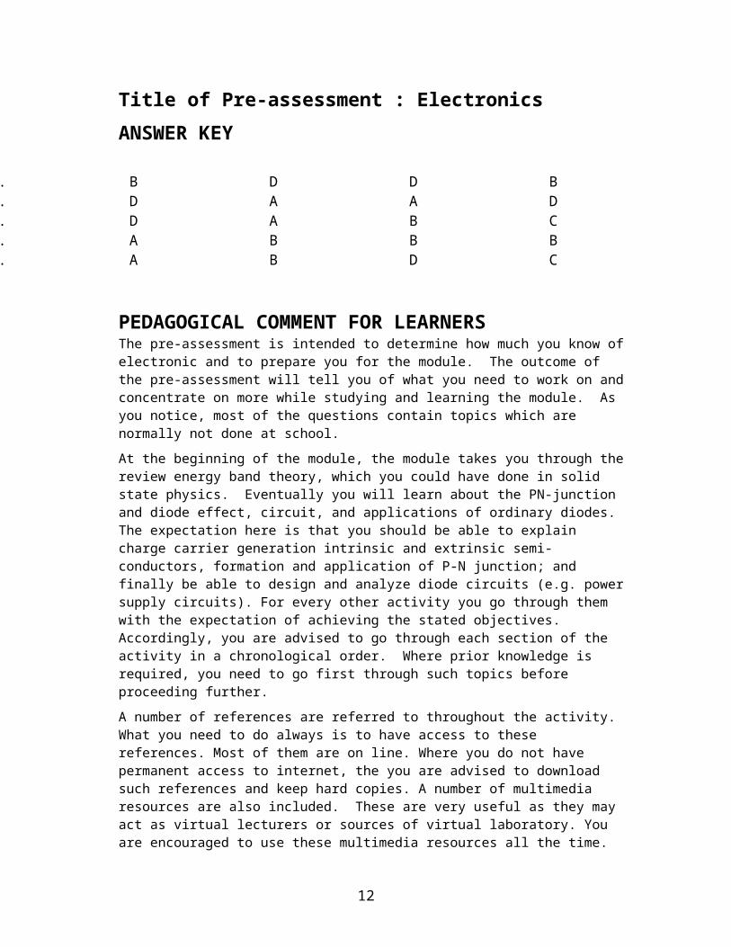
Title of Pre-assessment : ElectronicsANSWER KEY
1. B2. D3. D4. A5. A
DAABB
DABBD
BDCBC
PEDAGOGICAL COMMENT FOR LEARNERSThe pre-assessment is intended to determine how much you know of electronic and to prepare you for the module. The outcome of the pre-assessment will tell you of what you need to work on and concentrate on more while studying and learning the module. As you notice, most of the questions contain topics which are normally not done at school.
At the beginning of the module, the module takes you through the review energy band theory, which you could have done in solid state physics. Eventually you will learn about the PN-junction and diode effect, circuit, and applications of ordinary diodes. The expectation here is that you should be able to explain charge carrier generation intrinsic and extrinsic semi-conductors, formation and application of P-N junction; and finally be able to design and analyze diode circuits (e.g. power supply circuits). For every other activity you go through them with the expectation of achieving the stated objectives. Accordingly, you are advised to go through each section of the activity in a chronological order. Where prior knowledge is required, you need to go first through such topics before proceeding further.
A number of references are referred to throughout the activity. What you need to do always is to have access to these references. Most of them are on line. Where you do not have permanent access to internet, the you are advised to download such references and keep hard copies. A number of multimedia resources are also included. These are very useful as they may act as virtual lecturers or sources of virtual laboratory. You are encouraged to use these multimedia resources all the time.
8
ACTIVITY 1: Diode CircuitsYou will require 20 hours to complete this activity. Only basic guidelinesare provided to help you go through the activity. Personal reading and work is strongly advised.
Specific Teaching and Learning Objectives
In this activity you will
(i) Explain charge carrier generation in intrinsic and extrinsic semi-conductors.
(ii) Explain formation and application of P-N junction.
(iii) Design and analyse diode circuits (e.g, power supply circuits.
Summary of the learning activity This activity includes among others explanation of charge carrier generation, intrinsic and extrinsic semi-conductors; formation and application of P-N junction and finally how to design and analyse diode circuits (e.g, power supply circuits)
List of REQUIRED readings
Reading 1Complete reference: http://en.wikibooks.org/wiki/Electronics. 3rd October 2007.
Abstract: This is a complete textbook on electronics that deals with among others: analogue circuits: vacuum tubes; diodes, transistors; amplifiers; operational amplifiers, and analogue multipliers.
Rationale: Each of the topic is presented in very simple form that makes it easier for one to read through. However, these simply serve to supplement the learning process.
Reading 2. Reference: http://en.wikipedia.org/wiki/electronics. 5th October 2007.Abstract: This reading is formed from references obtained from many sites. Their URLs can be obtained from a soft copy of this reading. Basically all the essential topics of the course are covered in this reading 2.Rationale. The reference provide easy reading sources on electronics that a reader should have no problem using them.
List of relevant MULTIMEDIA resources.
Reference: http://www.educypedia.be/electronics/javacollectors.htm.Summary: This resource enables one to study Characteristics of NPN transistor. Rationale: The site gives an elegant simple virtual experiment that one can carry to study the characteristics of NPN transistor.
9
Reference: http://server.oersted.dtu.dk/personal/ldn/javalab/Circuit04.htmlSummary: The resource is for circuit of a primitive common-emitter (CE) amplifier
comprising an npn-transistor and external basis-, collector- and load resistors. The learner will find for a fixed set of component parameters the ranges of input voltage that make the transistor cut off, active or saturated, respectively. In the case of analogue applications the learner will determine the differential voltage amplification of the circuit when the transistor is in the active range. While for digital applications one is expected to find the smallest possible current gain (beta) and a corresponding collector resistance
that makes the circuit a functional logical inverter.Rationale: This resource serves to aid one in learning about npn transistor biasing.
Reference: http://server.oersted.dtu.dk/personal/ldn/javalab/Circuit01.htmlSummary: This resource gives a circuit of a Thevenin equivalent with a load in which
power P is delivered to the load. Rationale: This site provides a useful resource for learning about voltage divider.
List of Relevant Useful Links.
Title: Basic circuit analysishttp://ocw.mit.edu/OcwWeb/Electrical-Engineering-and-Computer-Science/6-002Circuits-and-ElectronicsFall2000/VideoLectures/index.htm.Abstract: These contain the course lecture slides accompanying video lectures, and description of live demonstration shown by the instructor.
Title: Diodes URL: http://jersey.uoregon.edu/~rayfrey/431/lab2_431.pdfhttp://jersey.uoregon.edu/Abstract: This site provides practical work V-I characteristics. In addition, the site
provides reading on transistor junctions, transistor switch and saturation etc.
Title: Diode applicationsURL: http://morley.eng.ua.edu/G332BW.pdf.Abstract: Various applications of diodes including power supply, half-wave rectifier,
bridge rectifier, full-wave rectifier with filter etc. are presented.
Detailed Description of the Activity (Main Theoretical Elements)
Activity 1.1 Review of energy band theory
Key Concepts about energy band theory
10
The key concepts one learns about energy band theory under solid state physics are:
(i) That the available energy states form what we call bands. (ii) That in insulators the electrons in the valence band are separated by a
large gap called forbidden energy gap from the conduction band. (iii) That insulators have empty conduction band, but a full valence band.
(iv) That in conductors like metals the valence band overlaps the conduction band, and therefore, there is no structure to establish holes. The total current in such conductors is simply a flow of electrons.
(v) That a semiconductor material is one whose electrical properties lie in between those of insulators and good conductors. In terms of energy band, semiconductors can be defined as those materials which have almost an empty conduction band and almost filled valence band. There is a small enough gap between the valence and conduction bands that thermal or other excitations can bridge the gap. With such a small gap, the presence of a small percentage of a doping material can increase conductivity dramatically.
(vi) That the outermost electrons of an atom i.e. those in the shell furthermost from the nucleus are called valence electrons and have the highest energy or least binding energy.
(vii) The band of energy occupied by the valence electrons is called the valence band and is the highest occupied band. It may be completely filled or partially filled with electrons but never empty.
Task 1.1
Important instruction1. For each task that you undertake you must make short notes using some of the references that are given to you and including those that you can have access to.
2. Use available electronic text books and other references e.g. http://hyperphysics.phy-astr.gsu.edu; to
(a) Revise your solid state physics and refresh your memory about the meanings of: energy band,valence band, conduction band, energy gap, and Fermi level.
(b) Make short notes about each one.(c) Distinguish between conductors, semiconductors, and insulators.(d) Sketch side by side, diagrams showing energy bands in conductors,
semiconductors and insulator.(e) Explain what is meant by intrinsic semiconductors; and binding energy.
11
Learning points 1.1
Under this section you learn:
(i) That the position of the Fermi level in relation to the conduction band is an important factor in determining electrical properties of materials.
(ii) That the large energy gap between the valence bands in an insulator says that at ordinary temperatures, no electrons can reach the conduction band.
(iii) That in semiconductors, the band gap is small enough that thermal energy can bridge the gap for a small fraction of electrons. In conductors, there is no band gap since the valence band overlaps the conduction band.
(iv) That for intrinsic semiconductors like silicon and germanium, the Fermi level is essentially halfway between the valence and conduction bands. Although no conduction occurs at 0 K, at higher temperatures the width of the forbidden energy bands is decreased and a finite number of electrons can reach the conduction band and provide some current. Conductivity of a semiconductor increases with temperature.
(v) That an intrinsic semiconductor is one which is made of semiconductor material in its extremely pure form. Alternatively an intrinsic semiconductor may be defined as one in which the number of conduction electrons is equal to the number of holes.
Activity 1.2: Origin of charge carriers
We can develop this concept by reminding ourselves of atomic structure and what valence electrons are.
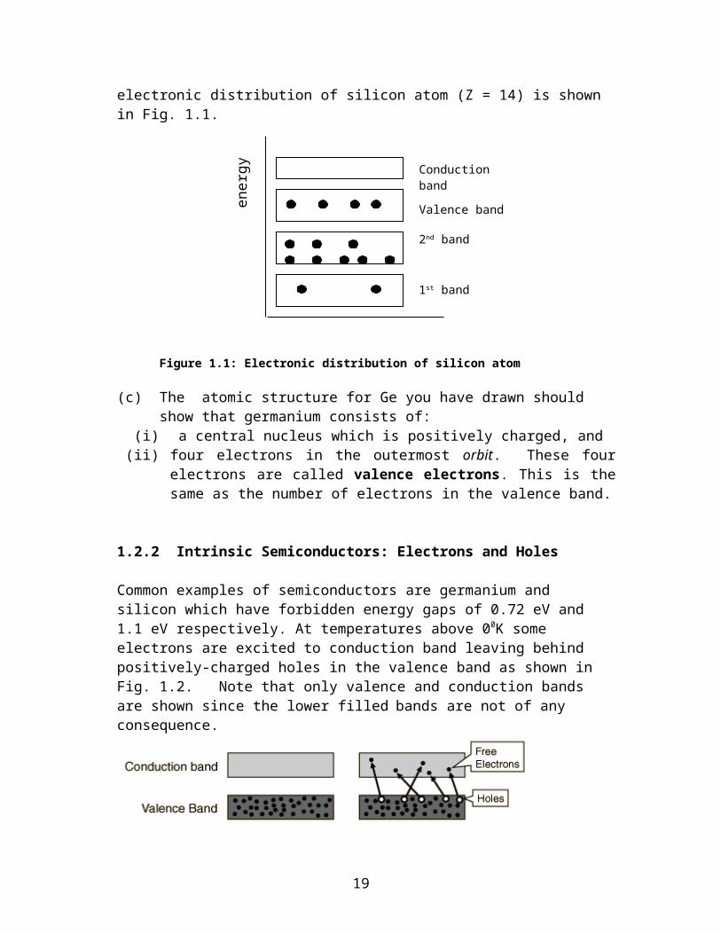
Task 1.2.1 In order to understand the origin of charge carrires, carry out the following tasks:(a) Read and write short notes on what is meant by atomic structure (b) Sketch the atomic structures of germanium (Ge) and silicon (Si). In addition to this, it is also a good practice to draw the electronic distribution of an element for comparison with the atomic structure. For example the electronic distribution of silicon atom (Z = 14) is shown in Fig. 1.1.
121st band
2nd band
Valence band
Conduction band
ener
gy

Figure 1.1: Electronic distribution of silicon atom
(c) The atomic structure for Ge you have drawn should show that germanium consists of:
(i) a central nucleus which is positively charged, and(ii) four electrons in the outermost orbit. These four electrons are called
valence electrons. This is the same as the number of electrons in the valence band.
1.2.2 Intrinsic Semiconductors: Electrons and Holes
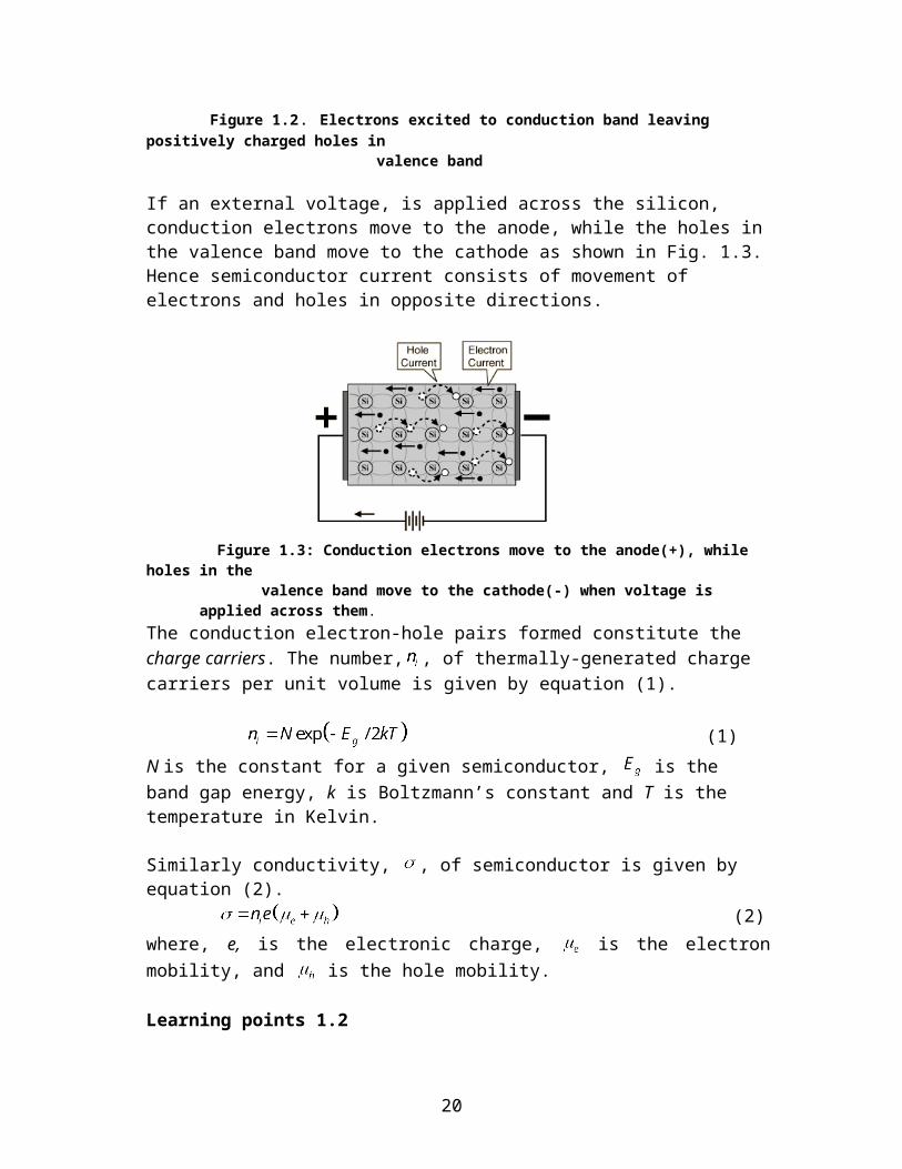
Common examples of semiconductors are germanium and silicon which have forbidden energy gaps of 0.72 eV and 1.1 eV respectively. At temperatures above 00K some electrons are excited to conduction band leaving behind positively-charged holes in the valence band as shown in Fig. 1.2. Note that only valence and conduction bands are shown since the lower filled bands are not of any consequence.
Figure 1.2. Electrons excited to conduction band leaving positively charged holes in valence band
If an external voltage, is applied across the silicon, conduction electrons move to the anode, while the holes in the valence band move to the cathode as shown in Fig. 1.3. Hence semiconductor current consists of movement of electrons and holes in opposite directions.
13
Figure 1.3: Conduction electrons move to the anode(+), while holes in the valence band move to the cathode(-) when voltage is applied across
them.The conduction electron-hole pairs formed constitute the charge carriers. The number, , of thermally-generated charge carriers per unit volume is given by equation (1).
(1)
N is the constant for a given semiconductor, is the band gap energy, k is Boltzmann’s constant and T is the temperature in Kelvin. Similarly conductivity, , of semiconductor is given by equation (2).
(2)where, e, is the electronic charge, is the electron mobility, and is the hole mobility.
Learning points 1.2(i) From electron configuration of atoms, the maximum number of electrons a shell can
have is ; in the nth shell, there are n sub-shell having different values of 1 such
as 0, 1, 2, …(n-1); Each sub-shell can accommodate a maximm of electrons.
(ii) Both Ge and Si have four electrons in the valence band or outermost shell.(iii) conduction electrons are found in and freely flow in the conduction band.(iv) holes exist in and flow in the valence band.(v) conduction electrons move almost twice as fast as the electrons.
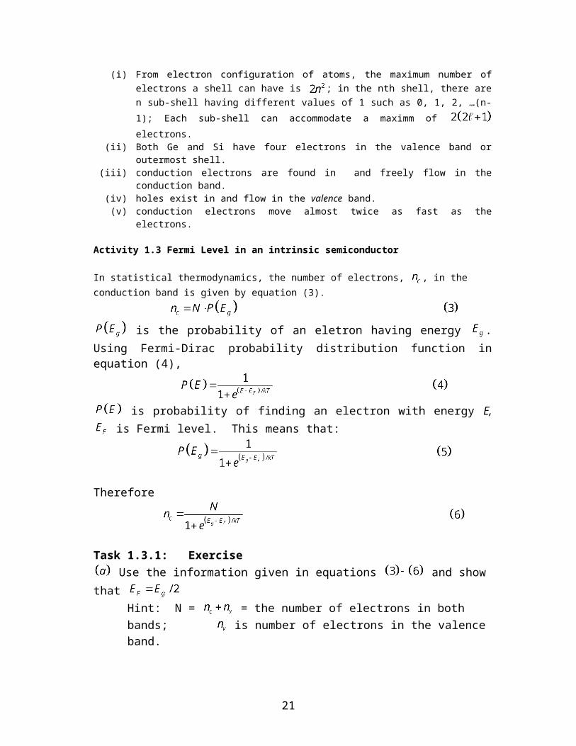
Activity 1.3 Fermi Level in an intrinsic semiconductor
In statistical thermodynamics, the number of electrons, , in the conduction band is given by equation (3).
is the probability of an eletron having energy . Using Fermi-Dirac probability distribution function in equation (4),
14
is probability of finding an electron with energy E, is Fermi level. This means that:
Therefore
Task 1.3.1: ExerciseUse the information given in equations and show that
Hint: N = = the number of electrons in both bands; is number of electrons in the valence band.
Learning points 1.3
Assumptions made are:(i) the width of energy bands are small compared to forbidden energy gap
between them.(ii) since band width are small, all energy levels in a band have the same
energy.(iii) energy of all levels in valence band are zero.(iv) energy of all levels in conduction band are equal to .
Activity 1.4 Extrinsic Semiconductors
Here you learn that:. A semiconductor is said to be doped when an impurity in an extremely
small quantity is added to it. Such semiconductors are called extrinsic or impurity semiconductors.
. The common doping agents are:(i) pentavalent atoms having five valence electrons (e.g. arsenic,
antimony, and phosphrous).(ii) trivalent atoms having three valence electrons (e.g. gallium, indium,
aluminium, boron).Pentavalent doping atom is known as donor atom. This is because they donate one electron to the conduction band of pure germanium Trivalent doping atom is called the acceptor because it accepts one electron from the germanium atom.Accordingly, two types of extrinsic semiconductors can be formed. These are: N-type semiconductors and P-type semiconductors.
15
Activity 1.4.1 N-Type Semiconductor N-type semiconductor can be formed when antimony is added to Si as impurity. An illustration is shown in Fig. 1.4 . Each atom of antimony forms covalent bonds with four germanium atom, but the fifth electron of antimony remains loosely bound to it. This free electron can easily be excited from the valence band to the conduction band on application of electric field or thermal energy.
Note that each atom of antimony introduced into germanium lattice contributes one conduction electron into germanium lattice without creating a positive hole.
Figure 1.4: (a) N-type semiconductor formed adding antimony to Si (b) P-type semiconductor formed by adding boron to SiThe donor atom becomes a positively-charged ion after giving away one of its valence electron, but it can not take part in conduction because it is firmly fixed into the crystal lattice. Addition of antimony greatly increases the number of conduction electrons. Thus the concentration of electrons in conduction band is increased and exceeds the concentration of holes in the valence band. In this situation, we see that in the N-type semiconductors electrons are the majority carriers, while holes constitute the minority carriers. When the number of charge carriers in the conduction band increases, the Fermi level shifts upwards towards the conduction band as shown in Fig 1.5(b).
Fig. 1.5 Showing relative positions of the Fermi level to conduction band
16
Activity 1.5: P-type Extrinsic SemiconductorHere you learn that:P-type extrinsic semiconductor is formed when a trivalent atom like boron is added to pure germanium crystal (or pure silicon crystal as shown in Fig. 1.4(b). The three valence electrons of boron atom form covalent bonds with four surrounding silicon atoms, but one bond is left incomplete. This gives rise to a hole.The acceptor impurity produces as many positive holes in silicon crystal as there are boron atoms and thefore a P-type (P for positive) extrinsic semiconductor is formed.In the P-type semiconductor, conduction is the movement of holes in the valence band. Holes form the majority carriers whereas electrons constitute minority carriers. Unlike in the N-type semiconductor, the Fermi level in P-type shifts towards the valence band, Fig 1.5(a) because, the majority carriers which are the holes are found in the valence band.
Activity 1.6: Conductivity of intrinsic Semiconductors
In an intrinsic semiconductor the total current, I , is due to the sum of electrons flow and hole flow. This is given by Eq. .
From equation , it can be shown that
/i e hI n e AV
Current density, where A is cross section area of semiconductor,V is voltage across its length, ,
is the electric field. The other symbols have their usual meanings.
Task 1.6.1 Note making and verfications of equations Use the available references and verify Eqs.
Hint: Note that in an intrinsic semiconductor, (the number of holes).
Activity 1.7: Conductivity of Extrinsic SemiconductorIn extrinsic semiconductors, current density, J, is given by Eqs. and .
For N-type semiconductor .
For P-type semiconductor .
where and are electron and hole densities in the N-type semiconductor after doping and and are electron and hole in the P-type semiconductor after doping.
17
Task 1.7.1 You need to try solving many numerical problems related to activity 1.6 in
order to develop sufficient confidence in this topic
Activity 1.7.2 DriftsIn this activity you will learn that:Directed motion of charge carriers in semiconductors occurs through two mechanisms:
i. Charge drift under the influence of applied electric field andii. Diffusion of charge from a region of high charge density to one of low
charge density.When an electric field is applied to a crystal, the charge carriers attain a direct motion which results into a net average velocity called drift velocity, v, in the direction of the applied electric field, E and produces a current. The relation between v and E is:
is mobility.The total current density due to electron and hole drift is
where n and p are electron density and hole density respectively.
Activity 1.7.3: DiffusionThe major concepts that you learn in this section are:
(i) Diffusion is a gradual flow of charge from a region of high density to a region of low density which eventually leads to an electric current without an applied field bieng applied.
(ii) The diffusion of carriers is proportional to the carrier density gradient, and the diffusion constant or diffusion coefficient D which has a unit of
. (iii) Current density due to hole diffusion is
. and
Similarly, current current density due to electron diffusion is.
.
Where = electron and hole diffusion constants respectively
= density gradient of electrons.
= density gradient of holes.
For simulation of diffusion of how the Fermi level varies with carrier concentration see: http://jas.eng.buffalo.edu/education/semicon/fermi/bandAndLevel/index.html.
18
http://jas.eng.buffalo.edu/education/semicon/fermi/bandAndLevel/index.html 10th October 2007.
Activity 1.7.4: Combined Drift and Diffusion currentsDrift and diffusion processes may be present simultaneously in semiconductors, thus the expressions for total electron and hole densities is given by Eq. .
Activity 1.7.5: Recombination(i) Recombination is also a phenomenon which occurs in semiconductors.
(ii) It results from the collision of an electron with a hole as free conduction electron return to the valence band.
(iii) Recombination is accompanied by the emission of energy. Besides all these, thermal generation of electron-hole pairs takes place continuously in semiconductors. Hence, there is net recombination rate given by the difference between the recombination and generation rates.
To learn more about diffusion, drift and recombination log to http://jas.eng.buffalo.edu/education/semicon/diffusion/diffusion.htmlhttp://jas.eng.buffalo.edu/education/semicon/diffusion/diffusion.html . 7th October 2007.
Activity 1.8: P-N JunctionIn this section you will learn that:
(i) A P-N junction is formed by joining together a doped P-type semiconductor and a doped N-type impurity semiconductor into a single piece of a semiconductor.
(ii) The plane that divides the P-type from the N-type semiconductors is called junction.
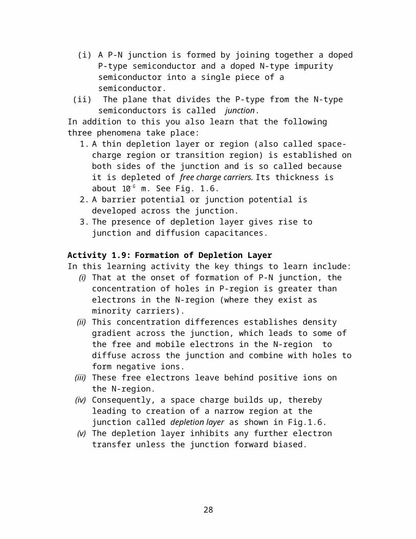
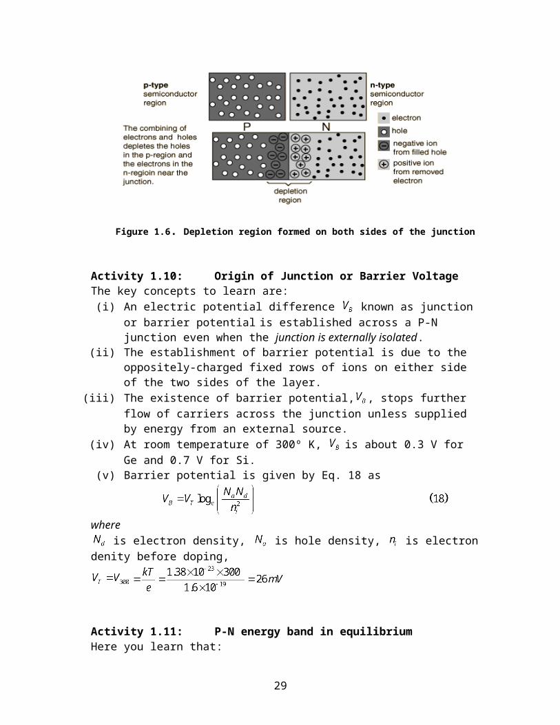
In addition to this you also learn that the following three phenomena take place:1. A thin depletion layer or region (also called space-charge region or
transition region) is established on both sides of the junction and is so called because it is depleted of free charge carriers. Its thickness is about m. See Fig. 1.6.
2. A barrier potential or junction potential is developed across the junction.3. The presence of depletion layer gives rise to junction and diffusion
capacitances.
Activity 1.9: Formation of Depletion LayerIn this learning activity the key things to learn include:
(i) That at the onset of formation of P-N junction, the concentration of holes in P-region is greater than electrons in the N-region (where they exist as minority carriers).
(ii) This concentration differences establishes density gradient across the junction, which leads to some of the free and mobile electrons in the N-region to diffuse across the junction and combine with holes to form negative ions.
19
(iii) These free electrons leave behind positive ions on the N-region. (iv) Consequently, a space charge builds up, thereby leading to creation of a
narrow region at the junction called depletion layer as shown in Fig.1.6. (v) The depletion layer inhibits any further electron transfer unless the
junction forward biased.
Figure 1.6. Depletion region formed on both sides of the junction
Activity 1.10: Origin of Junction or Barrier VoltageThe key concepts to learn are:
(i) An electric potential difference known as junction or barrier potential is established across a P-N junction even when the junction is externally isolated.
(ii) The establishment of barrier potential is due to the oppositely-charged fixed rows of ions on either side of the two sides of the layer.
(iii) The existence of barrier potential, , stops further flow of carriers across the junction unless supplied by energy from an external source.
(iv) At room temperature of 300º K, is about 0.3 V for Ge and 0.7 V for Si. (v) Barrier potential is given by Eq. 18 as
where is electron density, is hole density, is electron denity before doping,
Activity 1.11: P-N energy band in equilibriumHere you learn that:
20
(i) At equilibrium, the Fermi level match on the two sides of the junctions. Thus, electrons and holes reach an equilibrium at the junction and form a depletion region as in Fig.1.7.
(ii) The upward direction in Fig.1.7 represents increasing electron energy. This means that energy has to be supplied in order for an electron to go up on the diagram, and supply energy to get a hole to go down.
Figure 1.7. Position of Fermi level in P-N energy band in equilibrium
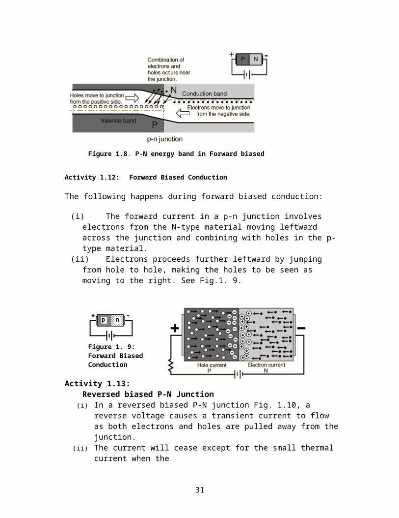
Activity 1.11: P-N energy band in Forward biasedIn this section you learn that when the p-n junction is forward biased, as shown in Fig. 1.8:
the electrons in the conduction band in the n-type material on diffusing across the junction find themselves at a higher energy than the holes in the p-type material.
As a consequence, they readily combine with those holes, making possible a continuous forward current through the junction.For demonstration of P-N junction diode under bias, seehttp://jas.eng.buffalo.edu/education/pn/biasedPN/index.html. 5th October 2007.
Figure 1.8. P-N energy band in Forward biased
Activity 1.12: Forward Biased Conduction
The following happens during forward biased conduction:
21
(i) The forward current in a p-n junction involves electrons from the N-type material moving leftward across the junction and combining with holes in the p-type material.
(ii) Electrons proceeds further leftward by jumping from hole to hole, making the holes to be seen as moving to the right. See Fig.1. 9.
Figure 1. 9: Forward Biased Conduction
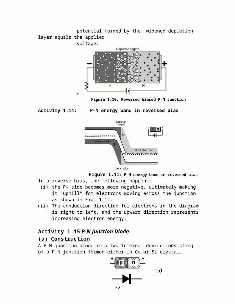
Activity 1.13: Reversed biased P-N Junction(i) In a reversed biased P-N junction Fig. 1.10, a reverse voltage causes a
transient current to flow as both electrons and holes are pulled away from the junction.
(ii) The current will cease except for the small thermal current when the potential formed by the widened depletion layer equals the applied voltage.
Figure 1.10: Reversed biased P-N Junction
Activity 1.14: P-N energy band in reversed bias
22
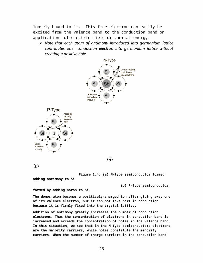
Figure 1.11: P-N energy band in reversed biasIn a reverse-bias, the following happens:
(i) the P- side becomes more negative, ultimately making it "uphill" for electrons moving across the junction as shown in Fig. 1.11.
(ii) The conduction direction for electrons in the diagram is right to left, and the upward direction represents increasing electron energy.
Activity 1.15 P-N Junction Diode(a) ConstructionA P-N junction diode is a two-terminal device consisting of a P-N junction formed either in Ge or Si crystal.
Figure 1.12: P-N Junction Diode
Its circuit symbol is shown in Fig. 1.12(b). The P- and N-type regions are referred to as anode and cathode respectively. In Fig. 1.12 (b), arrow-head indicates the conventional direction of current flow when forward-biased. It is the same direction in which hole flow takes place.
Activity 1.16: Applications of Diodes
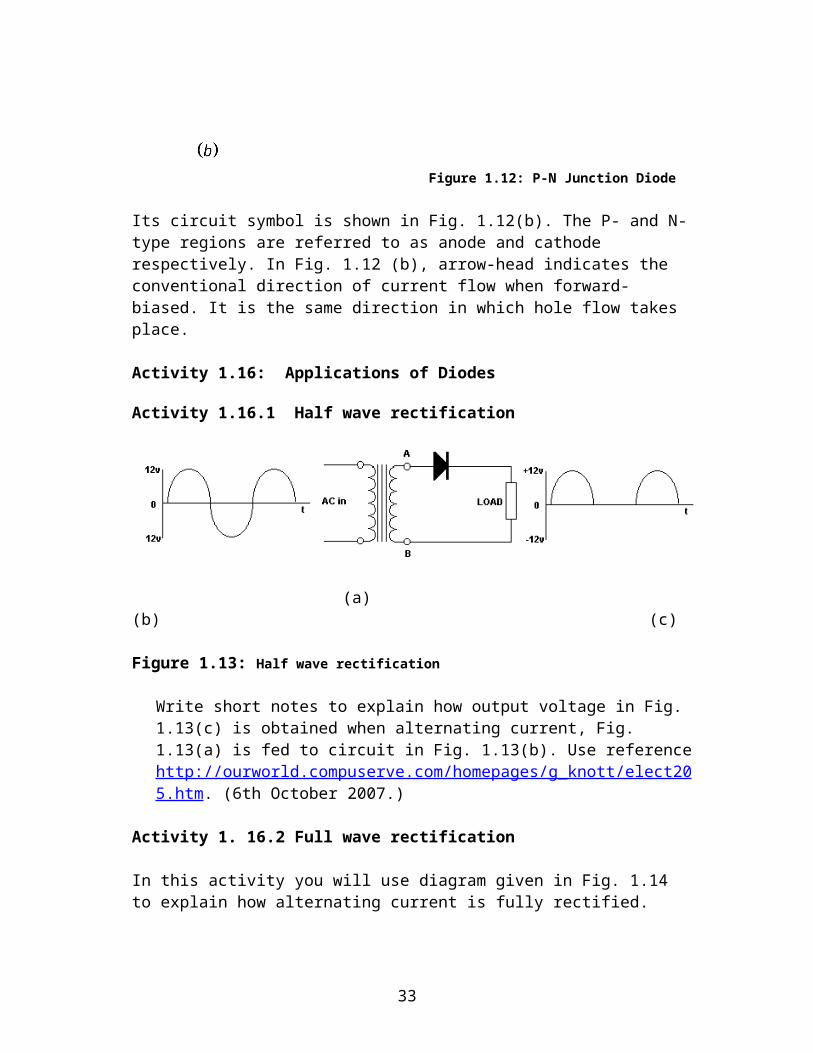
Activity 1.16.1 Half wave rectification
(a) (b) (c)
23
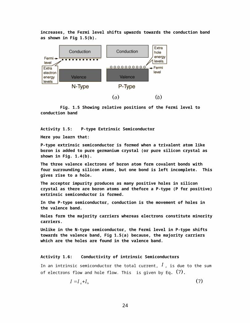
Figure 1.13: Half wave rectification
Write short notes to explain how output voltage in Fig. 1.13(c) is obtained when alternating current, Fig. 1.13(a) is fed to circuit in Fig. 1.13(b). Use reference http://ourworld.compuserve.com/homepages/g_knott/elect205.htm. (6th October 2007.)
Activity 1. 16.2 Full wave rectification
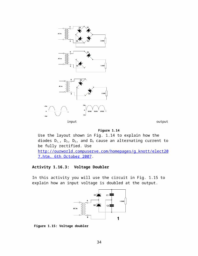
In this activity you will use diagram given in Fig. 1.14 to explain how alternating current is fully rectified.
input output
Figure 1.14Use the layout shown in Fig. 1.14 to explain how the diodes D1,, D2, D3, and D4 cause an alternating current to be fully rectified. Use http://ourworld.compuserve.com/homepages/g_knott/elect207.htm. 6th October 2007.
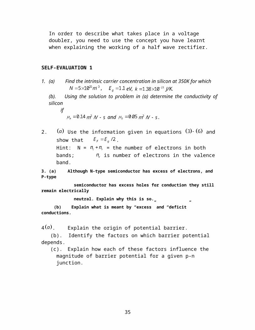
Activity 1.16.3: Voltage Doubler
In this activity you will use the circuit in Fig. 1.15 to explain how an input voltage is doubled at the output.
24
Figure 1.15: Voltage doubler
In order to describe what takes place in a voltage doubler, you need to use the concept you have learnt when explaining the working of a half wave rectifier.
SELF-EVALUATION 1
1. (a) Find the intrinsic carrier concentration in silicon at 350K for which eV, J/K.(b). Using the solution to problem in (a) determine the conductivity of silicon if and .
2. Use the information given in equations and show that
.Hint: N = = the number of electrons in both bands; is number of electrons in the valence band.
3. (a) Although N-type semiconductor has excess of electrons, and P-type semiconductor has excess holes for conduction they still remain electrically neutral. Explain why this is so. (b) Explain what is meant by “excess” and “deficit” conductions.
4 . Explain the origin of potential barrier. (b). Identify the factors on which barrier potential depends. (c). Explain how each of these factors influence the magnitude of barrier
potential for a given p-n junction.
25
ACTIVITY 2: Transistor CircuitsYou will require 25 hours to complete this activity. Only basic guidelinesare provided to help you go through the activity.
Specific Teaching and Learning Objectives
(i) Explain how a Bipolar Junction Transistor (BJT) works(ii) Design and analyse basic BJT circuits in various configurations (CE, EB, CB)
(iii) Explain how a junction Field Effect Transistor (JFET) works.(iv) Design and analyse JFET circuits in both configurations (CD, CS).(v) Explain how MOSFET works .
(vi) Design and analyse MOSFET circuits.
Summary of the Learning Activity
This activity is about the working of BJT. This includes among others forward-biased E-B junction; reverse-biased B-C junction, Voltage, current, and charge control, Transistor configuration, Transistor circuits, Leakage Currents in Transistor. A number of equations are also derived. These include among others the relation between transistor currents. Further the activity involves learning about transistor static characteristics, i.e. Input chracteristics; output characteristics; and Constant-current transfer characteristics. The last part of this activity is about the working of field effect transistor (FET) and MOSFET.
List of REQUIRED readings
Reading 1 Electronics WIKIBOOKSReference: http://en.wikibooks.org/wiki/Electronics. 5th October 2007.Abstract: Topics covered in this reading include: Analogue circuits, Digital circuits, Elements of Digital Circuits, Computer architecture, Analogue-to-Digital and Digital-to-Analogue converters.Rationale: The reading adequately covers the basic course of electronics outline in the activity.Reading 2. ElectronicsReference: http://en.wikipedia.org/wiki/electronics. 5th October 2007.Abstract: This reading is formed from references obtained from many sites. Their URLs can be obtained from a soft copy of this reading. Basically all the essential topics of the course are covered in this reading 2.Rationale. The reference provide easy reading sources on electronics that a reader should have no problem using them.
List of relevant MULTIMEDIA resources
Reference: http://jas.eng.buffalo.edu/education/semicon/fermi/bandAndLevel/index.html.
26
4th October 2007.Summary: The resource shows Fermi levels vs. carrier concentration and doping of
donor and acceptor impurities.Rationale: This aids in the learning of carrier concentration and doping of donor and
acceptor impuritiesReference: http://jas.eng.buffalo.edu/education/fab/BjtFet/index.html. 4th October 2007.Summary: The fabrication steps of a pair of Metal-Oxide-Semiconductor (MOS) Field Effect Transistor (FET) and a Bipolar Junction Transistor (BJT) on a Silicon wafer is illustrated in this applet. The four buttons, 'first', 'previous', 'next', and 'last' let you view the static images at various points of the device fabrication. The 'animate_next' button shows you through the animated 'time sequence' of the fabrication flow from this step to the next step. The animation capability teaches you most clearly the detailed physical steps involved. The fabrication steps of Semiconductor Devices involve many physical, chemical and thermal steps which this applet let you understand.Rational: This is a useful learning resource to use.
Reference: http://jas.eng.buffalo.edu/education/transistor/n_MOS_IV/mosfet.html. 4th October 2007.
Summary: The resource shows an applet which calculates and plots the output characteristics of an n-channel (enhancement-mode) MOSFET. Try to change the drain-source voltage (Vds) range and/or the gate bias starting value ('begin') or other values and see the drain current vs. drain bias (Vds) change Rationale: This is a useful resource for one to learn how to calculate and plot the output characteristics of an n-channel MOSFET.
List of relevant useful links
Title: MOSFET amplifier
URL: http://ocw.mit.edu/OcwWeb/Electrical-Engineering-and-Computer-Science/6-002Circuits-and-ElectronicsFall2000/VideoLectures/index.htm. 4th October 2007.
Abstract: This contains the course lecture slides accompanying videos lectures, and description of live demonstration shown by instructor during lectures
Title: BJT and FET transistorsURL: http://www.nhn.ou.edu/~bumm/ELAB/Lect_Notes/BJT_FET_transitors_v1_1.html.3rd October 2007.Abstract: This site provides good reading materials on BJT and FET transistor.
Title: Bipolar junction transistor.URL: "http://en.wikipedia.org/wiki/Common_collector. 4th October2007.
27
Abstract: This provides very good reading materials on structure of NPN, PNP, heterojunction bipolar transistor, transistor circuits and applications of transistors.
Title: CMOS.URL: "http://en.wikipedia.org/wiki/CMOS. 4th October 2007.Abstract: This site provides some good reading materials on structure of NAND gate, power switching, and leakage.
Title: Common SourceURL: "http://en.wikipedia.org/wiki/Common_source. 4th October 2007.Abstract: This provides some reading on characteristics of bandwidth.
Title: JFET.URL: "http://en.wikipedia.org/wiki/JFET”. 4th October 2007.Abstract: This is a source of good reading materials about JFET on the structure, function, schematic symbols, and comparison with other transistors.
Detailed description of activityIn this section, a mixture of the theory, instructions of what the learner should do while learning the module are prescribed. The learner is advised to complete fully each section of the module before moving to the next section or activity. For each section, the learner is advised to consult the references recommended. This is important because the instructions and activities described are in brief forms.
Activity 2.1: How a Bipolar Junction Transistor (BJT) works
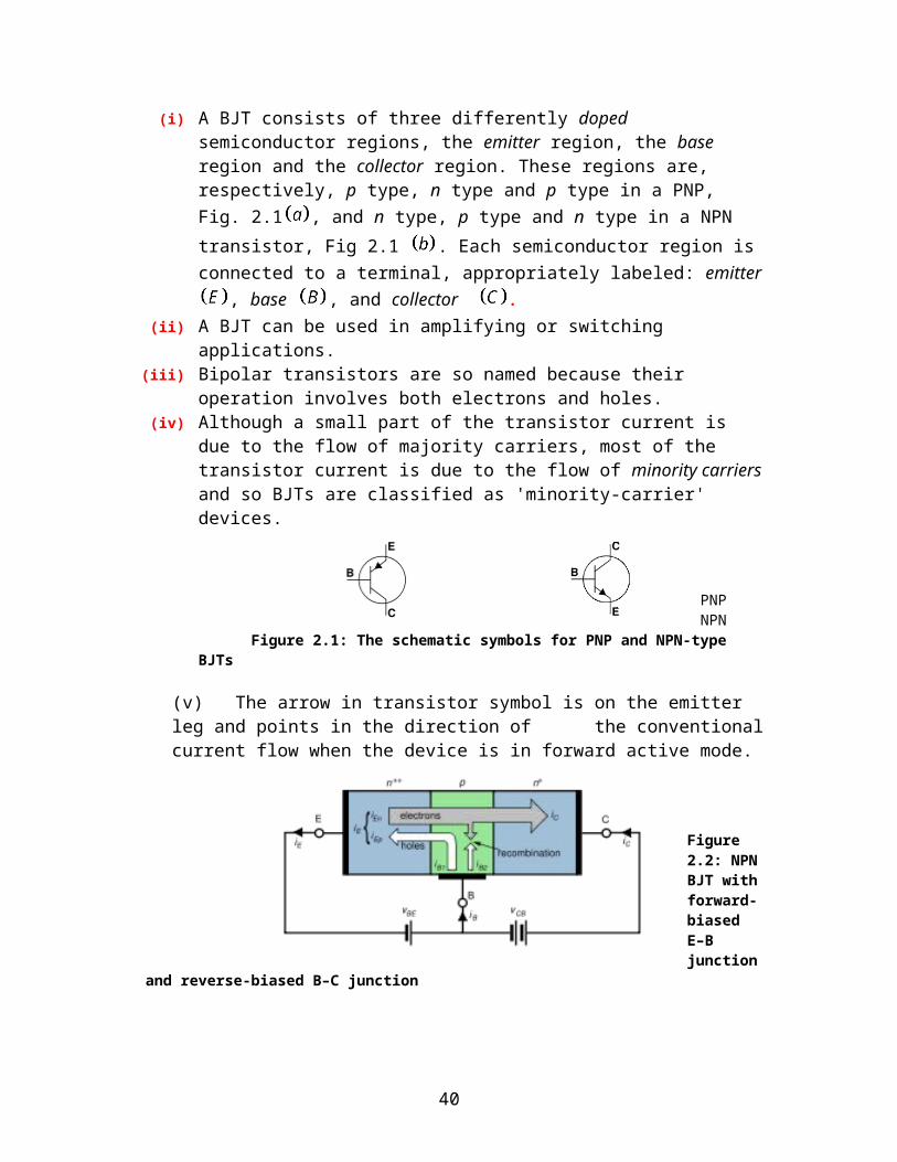
In this section you will learn how a BJT works and the key learning will include that:(i) A BJT consists of three differently doped semiconductor regions, the emitter
region, the base region and the collector region. These regions are, respectively, p type, n type and p type in a PNP, Fig. 2.1 , and n type, p type and n type in
a NPN transistor, Fig 2.1 . Each semiconductor region is connected to a
terminal, appropriately labeled: emitter , base , and collector .(ii) A BJT can be used in amplifying or switching applications.
(iii) Bipolar transistors are so named because their operation involves both electrons and holes.
(iv) Although a small part of the transistor current is due to the flow of majority carriers, most of the transistor current is due to the flow of minority carriers and so BJTs are classified as 'minority-carrier' devices.
PNP NPNFigure 2.1: The schematic symbols for PNP and NPN-type BJTs
28
(v) The arrow in transistor symbol is on the emitter leg and points in the direction of the conventional current flow when the device is in forward active mode.
Figure 2.2: NPN BJT with forward-biased E–B junction and reverse-biased B–C junction
(vi) In typical operation of NPN, the emitter–base junction is forward biased and the base–collector junction is reversed biased as shown in Fig.2.2
NB. In Fig. 2.2, the voltage between E and B is denoted as and that between C and
B as . The siginificance of the subscripts is that, the base is positive with respect to the emitter; and that, the collector is positive with respect to the base.
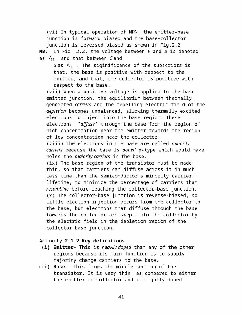
(vii) When a positive voltage is applied to the base–emitter junction, the equilibrium between thermally generated carriers and the repelling electric field of the depletion becomes unbalanced, allowing thermally excited electrons to inject into the base region. These electrons "diffuse" through the base from the region of high concentration near the emitter towards the region of low concentration near the collector. (viii) The electrons in the base are called minority carriers because the base is doped p-type which would make holes the majority carriers in the base.(ix) The base region of the transistor must be made thin, so that carriers can diffuse across it in much less time than the semiconductor's minority carrier lifetime, to minimize the percentage of carriers that recombine before reaching the collector–base junction. (x) The collector–base junction is reverse-biased, so little electron injection occurs from the collector to the base, but electrons that diffuse through the base towards the collector are swept into the collector by the electric field in the depletion region of the collector–base junction.
Activity 2.1.2 Key definitions(i) Emitter- This is heavily doped than any of the other regions because its main
function is to supply majority charge carriers to the base.(ii) Base- This forms the middle section of the transistor. It is very thin as
compared to either the emitter or collector and is lightly doped.(iii) Collector- Its main function is to collect majority charge carriers coming from
the emitter and passing through the base.(iv) The structure of NPN, BJT is shown in Fig. 2.3.
29
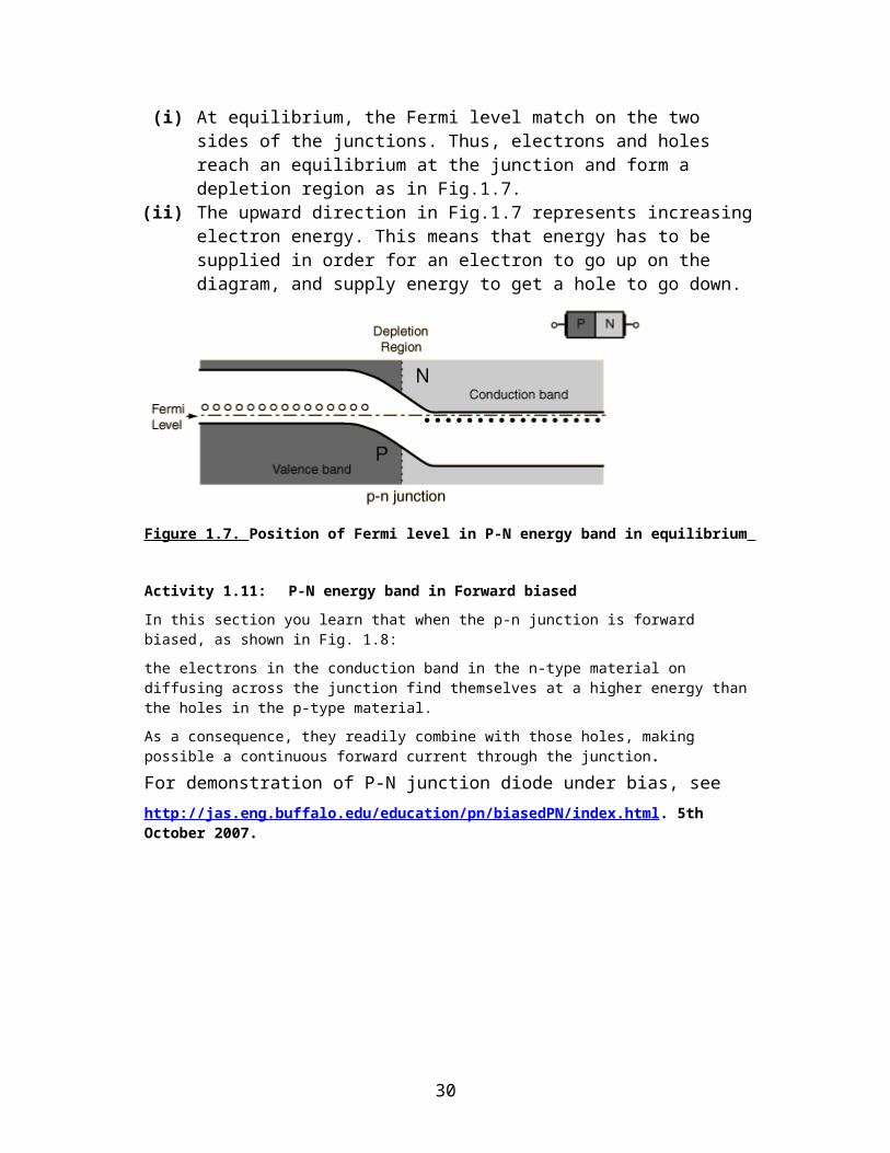
Figure 2.3: Structure of a NPN, BJT
(v) The collector region is much larger than the emitter region because it has to dissipate much greater power and also to collect much of the incoming charge carriers.
Task 2.1: Use "http://en.wikipedia.org/wiki/Bipolar_junction_transistor, (7th October 2007), and Theraja, ; and writeshort notes on:
(i) PNP transistors.(ii) How transistors are constructed.
(iii) List the key physical practical features of NPN, BJT.(iv) Five distinct regions of operation of BJT: Forward-active; Reverse-active; saturation; cutoff;
and Avalanche breakdown region.
Activity 2.1.3: Voltage, current, and charge control
Using reference "http://en.wikipedia.org/wiki/Bipolar_junction_transistor, (7th October 2007) you will learn that the collector-emitter current:
(i) can be viewed as being controlled by the base–emitter current (current control), or
(ii) by the base–emitter voltage (voltage control). (iii) These views are related by the current–voltage relation of the base–emitter
junction.(iv) The physical explanation for collector current is the amount of minority-carrier
charge in the base region. (v) In linear circuit design, the current-control view is often preferred, since it is
approximately linear. That is, the collector current is approximately (See equation 2.2) times the base current. The voltage-control model requires an exponential function to be taken into account.
Activity 2.1.4: Transistor configuration In this section you will learn about the three types of circuit connection of a BJT
1. There are three types of circuit connections for operating a transistor as shown in Fig.2.4.. common-base CB; . common-emitter CE; and . common-
collector CC.
30
where I/P is the input; O/P is the output.
Figure 2.4: Three types of Circuit connections of the BJT
The term common is used to denote the electrode that is common to the input and output.
2. For demonstration of common emitter amplifier, log to http://www.ngsir.netfirms.com/englishhtm/Amplifier.htm: 7August 2007.
Vary the different components as much as you can and observe and note the variation of the output varies.
3.For npn transisitor biasing see: http://server.oersted.dtu.dk/personal/ldn/javalab/Circuit04.html. 6th August 2007.
4. Single stage BJT amplier Analysis Applet: http://jas.eng.buffalo.edu/education/ckt/bjtamp/index.html# 6th
August 2007.
Activity 2.1.5: Transistors in circuits
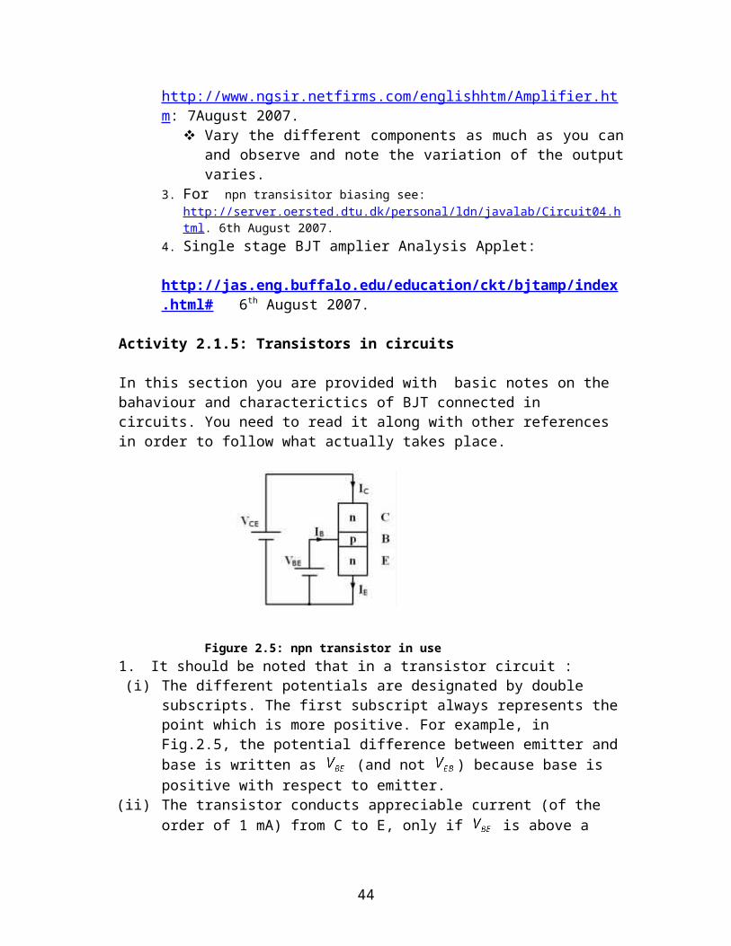
In this section you are provided with basic notes on the bahaviour and characterictics of BJT connected in circuits. You need to read it along with other references in order to follow what actually takes place.
Figure 2.5: npn transistor in use1. It should be noted that in a transistor circuit :
(i) The different potentials are designated by double subscripts. The first subscript always represents the point which is more positive. For example, in Fig.2.5, the potential difference between emitter and base is written as (and not ) because base is positive with respect to emitter.
31
B
E
C
I/P
O/P
I/P
B
C
E
O/PI/P
B
E 0VO/P
(ii) The transistor conducts appreciable current (of the order of 1 mA) from C to E, only if is above a threshold voltage sometimes referred to as the cut-in voltage, which is about 600 mV for silicon BJTs.
(iii) This applied voltage causes the lower p-n junction to 'turn-on' allowing a flow of electrons from the emitter into the base.
(iv) Because of the electric field existing between base and collector (caused by), the majority of these electrons cross the upper p-n junction into the collector to form the collector current, . The remainder of the electrons recombine with holes, the majority carriers in the base, making a current through the base connection to form the base current, . As shown in the diagram, the emitter current, , is the total transistor current which is the sum of the other terminal currents. That is:
(v) (vi) By normal convention, currents flowing into a transistor are taken as positive
whereas those flowing out of it are taken as negative. Hence, is positive whereas and are negative.
2. Key learning points The four basic guideposts about all transistor circuits are:
i. Conventional current flows along the arrow whereas electrons flow against it;ii. junction is always forward-biased;
iii. junction is always reverse-biased; iv.
Activity 2.1.6: Transistor 'alpha' and 'beta'
1. You need to learn about some key terms used in connection with transistors. The principle concepts to learn are that :
(i) The efficiency of a BJT is measured by the the proportion of electrons able to cross the base and reach the collector.
(ii) The heavy doping of the emitter region and light doping of the base region cause many more electrons to be injected from the emitter into the base than holes to be injected from the base into the emitter.
(iii) The common emitter current gain is represented by or . It is approximately the ratio of the DC collector current to the DC base current in forward-active mode and common-emitter configuration and is typically greater than 100.
(iv) Another important parameter is the common-base current gain, . This is approximately the gain of current from emitter to collector in common-base configuration. This ratio usually has a value close to unity; between 0.98 and 0.998. Alpha and beta are more precisely related by the following identities (NPN transistor):
32
For Demonstration Applets of BJT, log to http://jas.eng.buffalo.edu/. 6th August 2007.
For Fabrication steps of an FET and BJT: http://jas.eng.buffalo.edu/education/fab/BjtFet/index.html. 6th August 2007.
For high current gain, most of the carriers injected into the emitter–base junction must come from the emitter.
(i) Small changes in the voltage applied across the base–emitter terminals causes the current that flows between the emitter and the collector to change significantly. This effect can be used to amplify the input voltage or current. BJTs can be thought of as voltage-controlled current sources, but are more simply characterized as current-controlled current sources, or current amplifiers, due to the low impedance at the base.
(ii) Most bipolar transistors used today are NPN, because electron mobility is higher than hole mobility in semiconductors, allowing greater currents and faster operation.
1. An ac for a transistor in, CB configuration ,is the ratio of change in collector current to the change in emmitter current.
This is also known as the short-circuit gain of a transistor, and written as 2. Likewise in a CE configurations is given by
Eqs. .
Example: 2.1In a CB configuration, and in a transistor are 1.5 mA and 30 . Calculate
the values of and . Solution:
33
PNP
CI
BI
EI
CI
NPNEI
BI
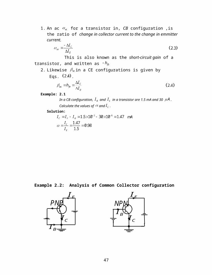
Example 2.2: Analysis of Common Collector configuration
Figure 2.6: Analysis of Common Collector configurationNote that the input is applied between base and collector, while ouput is taken out from emitter-collector Fig. 2.4. is the input current. Thus current gain is given by Eq. 2.5
Thus, Output current, input current
In both Fig. 2.6 and , .For demonstration of common emitter amplifier (demonstration of its working) see:
http://www.educypedia.be/electronics/javacollectors.htm. 10th August 2007.http://www.educypedia.be/electronics/composemiconductors.htm. 10th August 2007.
Summary of Learning activity.
Remember that relations between transistor currents are:
From Eq. You should be able to show that:
and that
The three transistor dc currents are in the following ratios
.
34
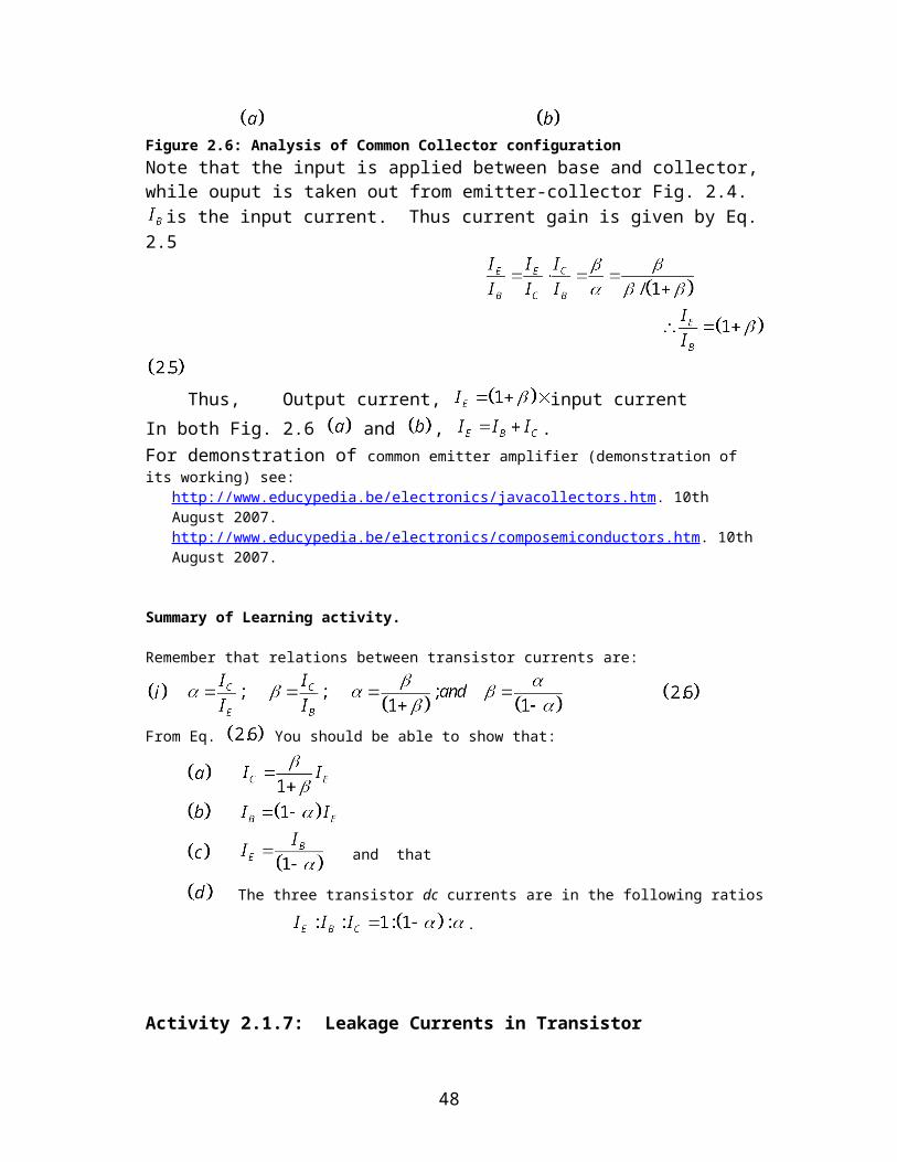
Activity 2.1.7: Leakage Currents in Transistor
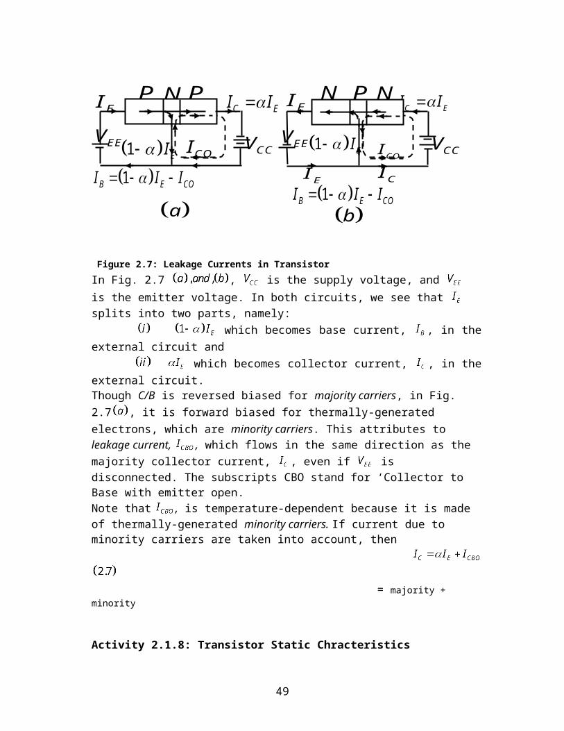
Figure 2.7: Leakage Currents in Transistor
In Fig. 2.7 , is the supply voltage, and is the emitter voltage. In both circuits, we see that splits into two parts, namely: which becomes base current, , in the external circuit and
which becomes collector current, , in the external circuit.
Though C/B is reversed biased for majority carriers, in Fig. 2.7 , it is forward biased for thermally-generated electrons, which are minority carriers. This attributes to leakage current, , which flows in the same direction as the majority collector current, , even if is disconnected. The subscripts CBO stand for ‘Collector to Base with emitter open.Note that , is temperature-dependent because it is made of thermally-generated minority carriers. If current due to minority carriers are taken into account, then = majority + minority
Activity 2.1.8: Transistor Static Chracteristics
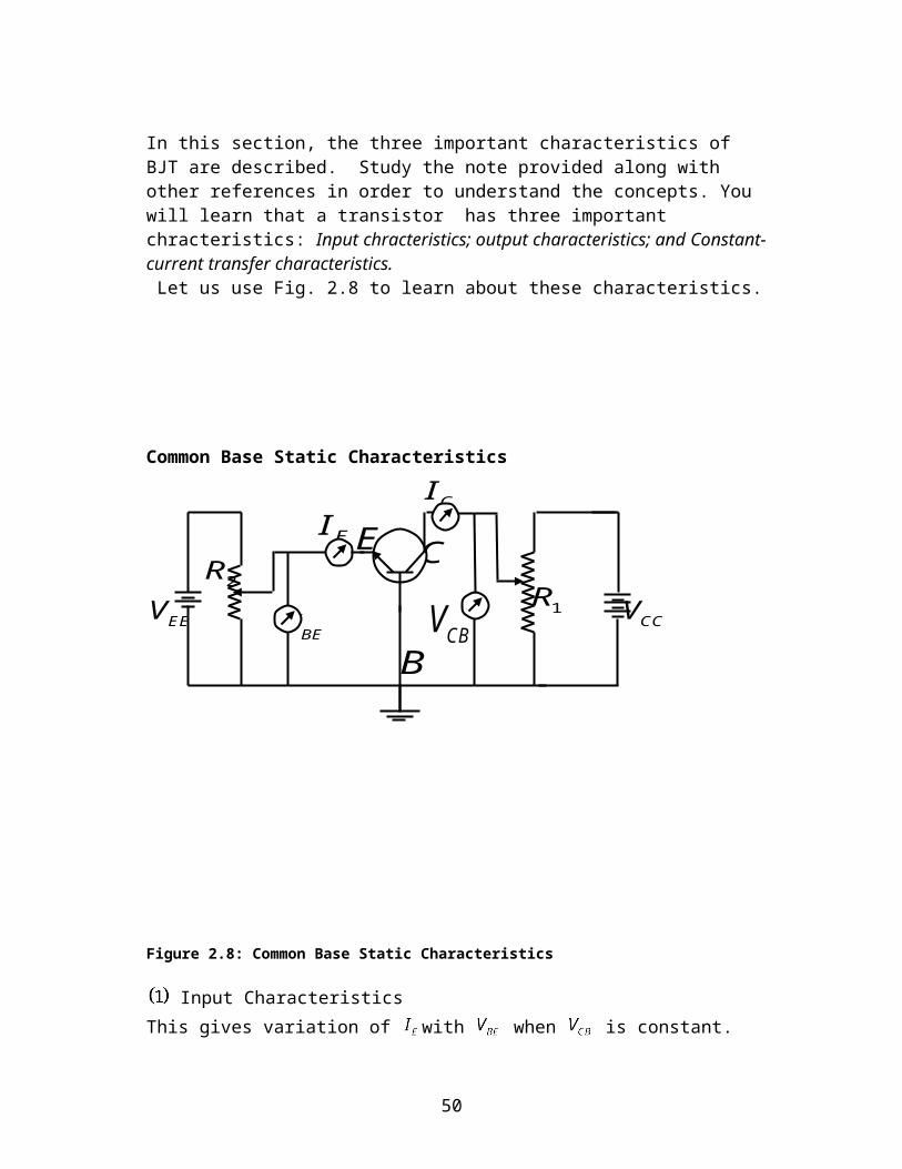
In this section, the three important characteristics of BJT are described. Study the note provided along with other references in order to understand the concepts. You will learn that a transistor has three important chracteristics: Input chracteristics; output characteristics; and Constant-current transfer characteristics. Let us use Fig. 2.8 to learn about these characteristics.
Common Base Static Characteristics
35
COI
N NP
CIEI
PNP
EEV
1B E COI I I
EI
CCV 1 EI
C EI I
COI EEV
1B E COI I I
EI
CCV 1 EI
C EI I
a b
BEV
B
ECI
EEV2R
CCV1RCBV
EIC
Figure 2.8: Common Base Static Characteristics
Input Characteristics
This gives variation of with when is constant.(i) Use the references at your disposal and describe how sets of values and are obtained
when is constant.
(ii) Sketch graphs showing variations of of with for different values of
(iii) On a given graph obtain instantaneous input resistance, , is obtained from the reciprocal of the slope. i.e.
Note that, variation in with usually gives rise to distortion of signals.
Output Characteristics: (Best done through experiment)This is a relation showing variation of with when is constant.
(i) The whole of activity 2.1.8 may be carried out experimentally. Get the components shown in Fig. 2.8 and carry out this activity practically.
(ii) In order to obtain the output characteristics, record corresponding values of and for different values of .
(iii) You should be able to note that the small amount of flows even when =0.
36
(iv) Use the characteristics obtained to find of the transistor.
Learning points(i) Beyond a certain value of , rapidly increases to a near saturation level due to
avalanche breakdown. This may damage the transistor.(ii) The small amount of which flows even when =0 is the collector leakage current .
(iii) The reciprocal odf the near horizontal part of the characteristics gives the output resistance, of the transistor which it woulf offer to input signal.
Current Transfer CharacteristicsThis is the relationship showing variation of with when is constant.
(i) Decribe how you may obtain corresponding values of and when is constant.
(ii) Typical transfer characteristics is calculated using the diagram given in Fig. 2.9.
The slope =
Figure 2.9: Current Transfer Characteristics(iii) If you have carried out this activity practically, determine the values of
.
Task 2.3: Further readings and Note makingRepeat activity 2.1.8 for Common emitter static characterics.
Common Colector Static Characteristics.
Activity 2.1.9: Different ways of Drawing Transistor Circuits
The essential concepts to learn here is how different transistor circuits can be drawn. The important learning point to remember is that in an NPN transistor, both collector and base have to be positive with respect to the emitter.Figures 2.10-2.12 show how power supply voltage can be represented with only one terminal of the battery, and the other terminal is understood to be grounded so as to provide a complete path for the current.
37
mA
mA
CI
EIEI
CI
Common Base configuration
Figure 2.10: Common Base configuration
Fig. 2.10 can be redrawn as shown in Fig. 2.10 in which the negative terminal of and positive terminal of are supposed to be grounded.
Common Emitter Configuration
Figure 2.11: Common Emitter Configuration
38
PNPER20K
10VEBV
LR
10KCCV25V
EI
( )a
BCVEBV
CIEI
LR10K20KER
25CCV V10EEV V
PNPCB
B
BR
1M
BBV10V
BEV
LR
10K
CCV
20VCEV
EI
CI
BI
( )a
CEVBEV
CIBI
LR10K1M BR
CCVBBV
NPN
EI
( )b
NPNsignal
+9V-
SD
A more popular way of indicating power supply voltages in Fig. 2.11 is given in
Fig. 2.11 . Since both collector and base are positive with respect to emitter, a single battery can be used.
Sketch a new circuit for 2.11 in which there is only one battery.
Common Collector Configuration
Figure 2.12
The power supply voltages in Fig. 2.12 for CC configuration can be redrawn as
shown in 2.12 .
Numerical Examples Calculations of voltages and currents in the circuits
Consider Fig. 2.10 . Starting from the ground and applying Kirchoff’s law for the left part of the circuit, we have
For Si, V mA
In most cases . Thus
mA
State the reasons for this approximation.
39
BI
CI
+
+ + + +
NPN
CICBVBBV
EEVBR
EREI
CEV-
+
++++CBV CEVNPNBR ER
EIBI
+-
p-type gate region
DG
SN
Similarly the circuit on the right, and starting from the ground, we have
V
Activity 2.2: Field Effect Transistors You will learn that:
(i) Field effect transistors are also three-terminal devices, which is widely used in linear and digital integrated circuits.
(ii) In a FET only one type of charge carrier is involved in its action, the electron or positive hole. On this account, FET is called a unipolar transistor
(iii) There are two common types of field effect transistors: junction field effect transsitor ; and metal-oxide semiconductor field effect
(iv) One important advantage FET has over BJT is a very high input impedance.
Activity 2.2.1: Action of JFET n-type channel
Figure 2.13: n-type channel
The features in Fig. 2.13, include:(i) S and D which are two connections called the source and drain respectively.
When these are connected to a d.c power supply, electrons flow through the channel from the source, S, to the drain, D.
(ii) A p-type region called the gate, G which is alloyed into the n-channel. This is input controlling electrode.
For demonstration see: http://jas.eng.buffalo.edu/education/pn/biasedPN/index.html. 8th August 2007.N-channel JFET: http://www-g.eng.cam.ac.uk/mmg/teaching/linearcircuits/jfet.htmlJFET: http://jas.eng.buffalo.edu/education/jfet/index.html#. 8th August 2007.
Task 2.4 Note making Write short notes on the formation of depletion regions when the gate, G, is made
negative with respect to the n-channel as shown in Fig. 2.13. Describe how the magnitude of the applied voltage determines the width of the depletion layer, the resistance of the channel, and the value of the drain current.Sketch FET symbols and basic d.c circuits for both n-channel and p-channel.
Use output characteristics of FET, to show that the a.c. output resistance, , is the slope of the output, where the current levels off. That is:
40
0.2DI mA DI
6
2GS VV
DSV2 100.1
a.c. output resistance, = when constant
Use also mutual characteristics, to show that mutual conductance which is concerned with the sensitivity of the gate control on the drain current is given by Eq. 2.10. That is:
Mutual conductance, when is constant
Activity 2.2.2: Pinch Off The major concept that you will learn here is about the relation between depletion region with changes in potential between S and D.
Figure 2.14: showing the pinch-off
Observations made: 1. As the distance from S towards D increases:
(i) the channel potential become more positive; (ii) the reverse p.d between the gate and channel increases towards D, and
(iii) the width of the channel between the depletion region decreases along the length of the gate.
2. Increasing the positive voltage on the drain causes the depletion regions to come together at the drain end, thus pinching-off the current at a certain value.
Numerical Example
Use Fig. 2.15 and to calculate the value of when is -2 V and the
value of mutual conductance, when is 6 v and is -2 V.
41
Pinch-off point channel
+-
Depletion region region
DG
S
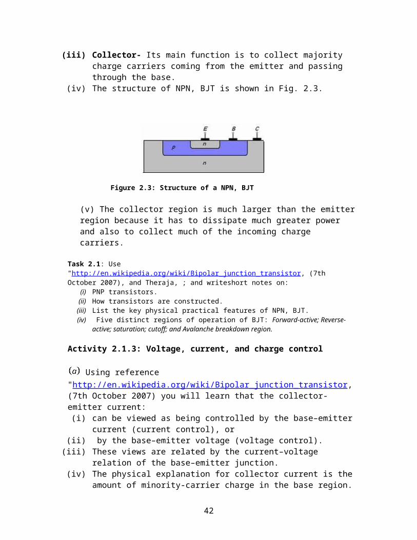
Figure 2.15
From Eq. 2.9, = =
From Eq. 2.10, mA/V
Activity 2.2.3: FET equivalent a.c. circuit
42
1.5GSV V
3
2
1
6DSV V
-1-2-3
DI
GSV
signal iV
iV
m i
m gs
g V
g V
D
S
DRdr1M
DR
-
+9V
0V0.1
0V
FET equivalent circuit Basic FET amplifier circuit
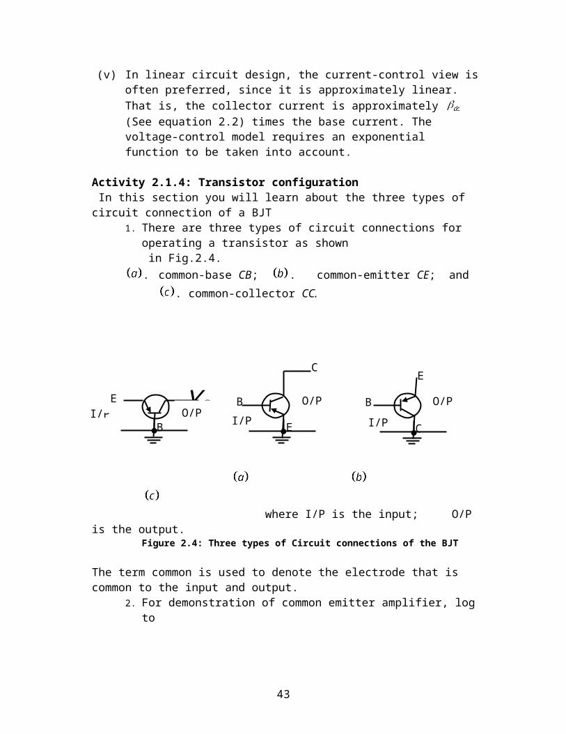
Figure 2.16
You will learn that in FET(i) Very small leakage flows between source and gate.
(ii) Source current = Drain current.(iii) Gate-to-source capacitance is very small, while in BJT it is much higher.
Illustration of basic FET amplifier Circuit.
(i) In Fig. 2. 16 the purpose of the capacitor is to isolate the signal source from the gate as far as d.c. is concerned.
(ii) The value of the capacitance, C, has to be large enough to diminish the signal. In this case, the value of the frequency, f, is calculated for C = 0.1 and reactance = 1 as follows.
Hz.
Equivalent a.c. CircuitThe equivalent circuit of Fig.2.16 is given in Fig. 2.16 is drawn after identifying that:
(i) is connected between drain and the source.(ii) The output resistance, , inside FET between the drain and source is parallel
to .(iii) The signal voltage or develops a signal current which
divides between , and .
Activity 2.2.4: Voltage gain at Mid-frequency
Middle range of frequencies in a.f. band lies between 300 Hz and 5000 Hz.
Voltage gain
are r.m.s values. From Fig. 2.16 ,
where , and are in parallel.
43
Numerical ExampleA field effect transistor having = 4 mA/V and =60 is used with a drain load resistance of 30
in a.f. voltage amplifier. Find the voltage gain.
Solution
Task 2.5: Note making and further readingUse the references and make notes on
i. Output and output phase relationii. Gate biasing
iii. Load line calculations
Activity 2.2.5: MOSFET
1. Structure(i) MOSFET is a form of FET where the gate is insulated from the channel by a
thin layer of silicon oxide as shown in Fig. 2.17.(ii) Accordingly, in a MOSFET,
- no leakage of current between gate and channel occurs and- the input resistance is of hundreds of megohms.
Figure 2.17: Construction of MOSFET (depletion type)
Note that the gate is coupled by capacitance effect through the oxide and channel.
When gate is provided with positive bias, a field is set up through the oxide which attracts electrons to the gate region. This conduction takes place between source and drain. The degree of conduction depends on how positive the gate is with respect to source.
44
DGS
N-channel
Base
P-substrate
Silicon oxide
For: n-channel MOSFET output characteristics see: http://jas.eng.buffalo.edu/education/transistor/n_MOS_IV/mosfet.html. 10 th August 2007.
Task 2.6: Note making and further readingUse the references and complete the notes on:-output characteristics curves when the magnitude of positive bias in MOSFET is varied
SELF EVALUATION 2
1. Carry out the analysis of CE and show that .
Hint: Write the relation for in terms of collector and base currents first.2. Show that in a CC configuration
Output current input current3. With reference to a transistor
Show that and
Similarly, show that
Repeat activity 2.1.7 for CE Circuit
45
ACTIVITY 3: Operational Amplifiers
You will require 10 hours to complete this activity. Only basic guidelinesare provided to help you go through the activity.
Specific Teaching and Learning Objectives
In this activity you will be required to:i. Explain the construction of operational amplifier, and
ii. Design, analyse and synthesize operational amplifier circuits.
Summary of the learning activity
The activity involves learning about the general features of an operational amplifier, the principles behind its operation and its applications in classical computation which include addition, subtraction, multiplication, division, integration and differentiation. Relevant equations are derived and used to solve numerical problems.
List of REQUIRED readings
Reading 1 Electronics WIKIBOOKSReference: http://en.wikibooks.org/wiki/Electronics. 5th October 2007.Abstract: Topics covered in this reading include: Analogue circuits, Digital circuits, Elements of Digital Circuits, Computer architecture, Analogue-to-Digital and Digital-to-Analogue converters.Rationale: The reading adequately covers the basic course of electronics outline in the activity.
Reading 3: Operational Amplifier WIKIBOOKS
Reference: http://en.wikibooks.org/wiki/Electronics/Op-Amp. 5th October 2007.Abstract: Reading 3 include: Amplifiers, op-amp, notation, quick design process, ideal op-amps, basic op-amps configuration, advanced op-amp configurations and real op-amp.Rationale: This provides most of the required reading on operational amplifier that is needed for the course.
List of relevant MULTIMEDIA resources.
Reference: http://server.oersted.dtu.dk/personal/ldn/javalab/Circuit03.html . 3rd October 2007.
46
Summary: This resource is on inverting amplifier where the voltage source is turned on in order to check the circuit for different values of the resistances and/or the open-loop gain of the opamp.Rationale: In the (normal) case of a large open-loop gain of the opamp (typically >100 dB) the feedback mechanism will force the inverting input terminal to be virtually grounded. In this limit the closed-loop amplification factor of the circuit will be determined solely by the resistance values.
List of Relevant Useful Links.Title: Operational amplifier.URL: http://ocw.mit.edu/OcwWeb/Electrical-Engineering-and-Computer-Science/6- 002Circuits-and-ElectronicsFall2000/VideoLectures/index.htm. 3rd October 2007.
Abstact: These contain course lecture slides accompanying video lectures, and descriptions of live demonstration shown by instructor during lectures.
Title: OP-Amps.URL: "http://en.wikibooks.org/wiki/Electronics/Op-Amps". 4th October 2007.Abstract: Provides good reading materials on amplifiers, Op-Amp, notation, ideal Op-
Amps, basic Op-Amp configurations, and real Op-Amp.
Title: Operational Amplifier.URL: "http://en.wikipedia.org/wiki/Operational_amplifier. 4th October 2007.Abstract: This has good reading materials on operational amplifier. The topics include: basic operation, the ideal op-amp, limitations of real op-amps, notations, use of electronics system design, DC behaviour, AC behaviour, Basic non-inverting amplifier circuit, internal circuitry of 741 type of op-amp, and common applications.
Activity 3.1: Construction of operational amplifierUsing references like: "http://en.wikipedia.org/wiki/Operational_amplifier 6th August 2007.You will learn that Operational amplifier:
(i) is usually abbreviated as an op-amp, and its usual circuit symbol is shown in Fig. 3.1
(ii) has two inputs and one output, where the inputs are assumed to have very high impedance and therefore negligible current flows into or out of the inputs.
(iii) has output which is controlled by a negative feedback in ordinary usage.
(iv) has an output voltage of an input is determined by the negative feedback because of the amplifier’s high gain.
(v) has ideally an output impedance of zero. This means that an op-amp can deliver an infinitely large current to the load or circuit connected to it.
47
(vi) Makes all classical computation possible including addition, subtraction, multiplication, division, integration and differentiation.
where:
V+: non-inverting input V−: inverting input
Vout: output VS+: positive power supply (sometimes also VDD, VCC, or VCC + ) VS−: negative power supply
(sometimes also VSS, VEE, or VCC − )
Figure 3.1:Circuit symbol for an op-amp
The commonest type of op-amp is the “741”. It has 8 pins. Fig. 3.2 gives their physical appearance.
Figure 3.2: Typical physical appearance of 741 Op-amp
Activity 3.2: Basic non-inverting amplifier circuitIn this activity you will learn that :
The output voltage is the difference between the + and - inputs multiplied by the open-loop gain: .
48
inV outV_ inV
outV
V
V
V outV
_
SV
Inverting amplifier Non-inverting amplifierFigure 3.3: Basic inverting and non-inverting amplifier circuits
(i) If an op-amp is connected as in Fig. 3.3 and , the ratio of would be very high. This is called open-loop gain. When an Op-amp is operated without connecting any resistor or capacitor from its output to any one of its input (i.e., without feedback), it is said to be in the open-loop condition. The word “open loop” means that the feedback path or loop is open.
(ii) In a non-inverting arrangement, the output, , is in phase with the input voltage and is an exact amplified copy of the input, but
(iii) In this case of inverting arrangement, the output voltage is exactly opposite, amplified copy of input voltage i.e. output voltage is 180 degrees out of phase with input voltage.
Task 3.1: Further reading and note making
Use the following references:
1. "http://en.wikipedia.org/wiki/Operational_amplifier. 12 August 2007.2. B.L Theraja and R.S. Sedha: “Principles of Electronic devices and circuits”
a. Make complete notes about non-inverting amplifier circuit b. State the two “golden rules” as you make the note.c. Make notes on the difference between open loop gain and closed
loop gain
For simulation of an inverting amplifier see: http://server.oersted.dtu.dk/personal/ldn/javalab/Circuit03.html. 7th July 2007.http://www.ngsir.netfirms.com/englishhtm/Amplifier.htm: : http://server.oersted.dtu.dk/personal/ldn/javalab/Circuit03.html
Activity 3.2.1: Negative Feedback
Figure 3.4: Negative Feedback
49
x
3R
1R
2R
inVoutV
_
Negative feedback occurs when a little of the output signal is fed back to the inverting input using circuit arrangement in Fig. 3.4. Since is 180 out of phase with input, the feedback reduces the signal the amplifier has to amplify and therefore reduces the gain. The amount of output fed back is controlled by .
Some of the advantages in using negative feedback are:1. Amplifiers with almost infinitely variable gain can be produced using one standard Op amp circuit2. The use of negative feedback improves the range of frequencies that the amplifier will amplify and improve stability.
Some OP amp characteristics (i) There is a very high impedance between the + and the – input and
ground. Idealy this impedance is infinite but in practice it is approximately 2 . This ensures that no current flows into the amplifier input terminals
(ii) There is zero output impedance which ensures that the amplifier is unaffected by load
Short noteDue to the high open loop gain, a slight difference between + and – input voltages makes the output go to its highest value which is the voltage of the supply. This is called the saturation value, as the output can go no higher. If the voltage supply is 15V and the open loop gain is 105 then the difference in voltage of 15/105 =150 produces saturation. With a any small difference in voltage, can swing from +15 V to -15 V or the other way. NB. Sketch the variation of with for this observation For the amplifier to be of any use, the – input must be at virtually the same voltage as the + input. In the inverter amplifier circuit the + input is connected to earth which is also 0 V, so the – input must be always virtually at the same voltage. The – input is known as a virtual earth
Activity 3.2.2: Gain of Inverting AmplifierIn Fig. 3.3 the input is kept balanced as far as possible if resistor is connected between + input and 0V, in parallel to .
Since the + input is at earth potential (virtual earth) the current through will be and the current through .
Since the input impedance is very high, no current can flow into the – input. Therefore the sum of currents at junction X must equal to zero. i.e.
50
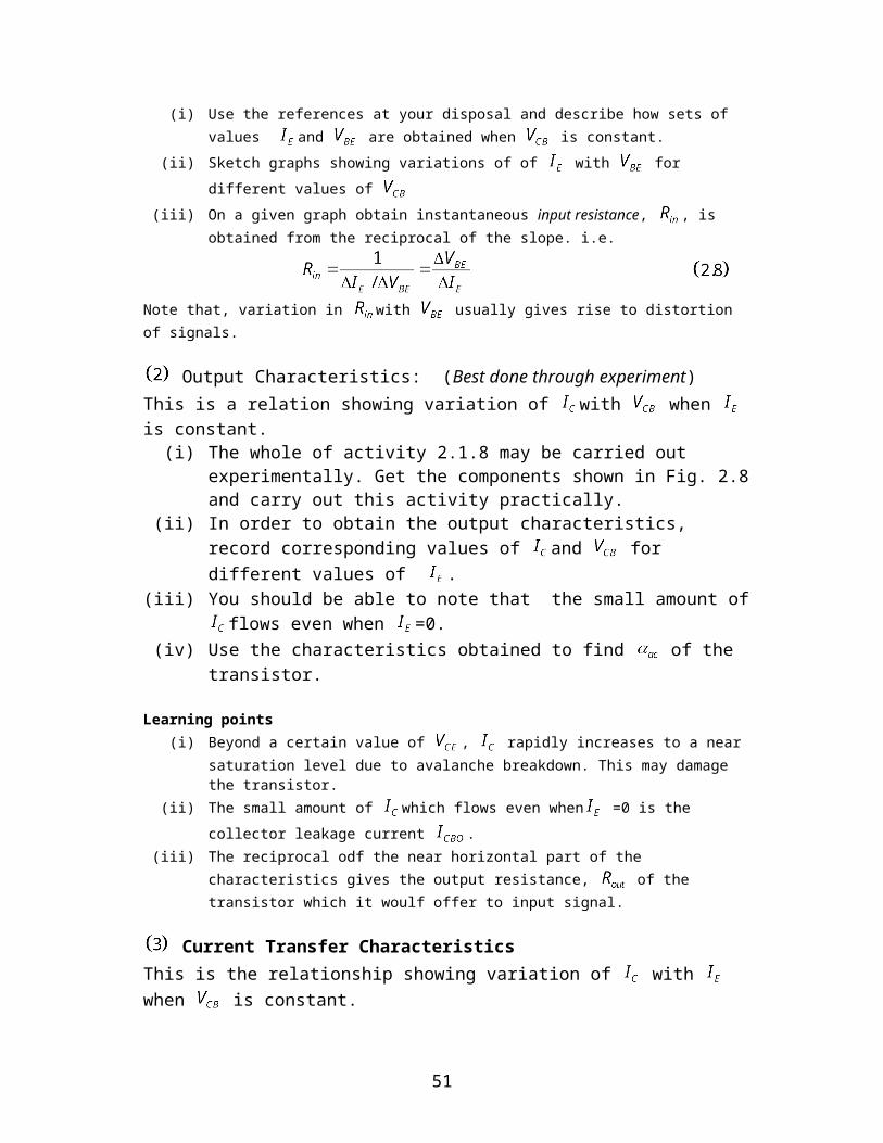
But
So gain of this inverting amplifier = . The minus sign indicates that the output is inverted. The gain depends on . This means that the gain is not affected by any changes that may take place inside the op-amp, such as a change in gain due to temperature change. So the negative feedback provides stability.
Task 3.2: Further reading and note makingUse the references and make notes on 1. Gain of non-inverting Amplifiers.2. Voltage follower.3. Frequency Response of op-amp Circuit.
Activity 3.2.3: Gain of non-inverting Amplifier
Using Fig. 3.4, the gain of non-inverting amplifier is derived as follows.
Figure 3.5: Gain of non-inverting AmplifierThe input is applied to the + input, but the feedback is applied to the – input as shown in Fig. 3.5. The fraction of the output signal to be fed back to the input is determined by the potential divider ..
Let the fraction of sent to the inverting (-) input is , where
.Let the voltage difference between the two inputs be where.
In this case, is the voltage amplified i.e..
is the open-loop gain. Thus, substituting for in Eq. using Eq. we get
and
.
51
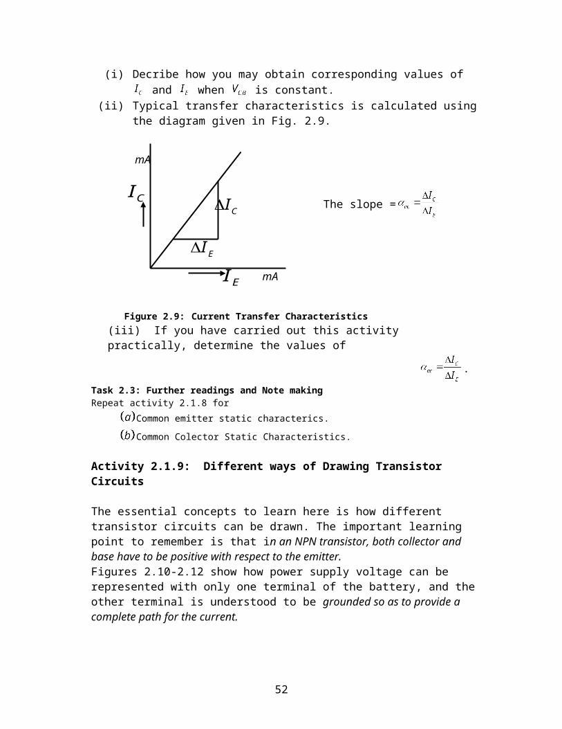
Again, substituting for in Eq. using Eq. we have
From Eq. 3.7, gain depends on .
ExampleCalculate the output voltage in a noninverting amplifier for an input of 120 if R1 = 2.4 k and .Solution
The gain of an op-amp circuit is given by
The output voltage is then.
Activity 3.2.4: Op-amps as summing amplifier
An op-amp is used in audio pre-amplifiers and mixers. When used to add any number of signals or voltages, the circuit is called a summing amplifier, Fig. 3.6
Point x is a virtual earth, therefore input currents into point X are
And feedback current =
By Kirchoff’s law
52
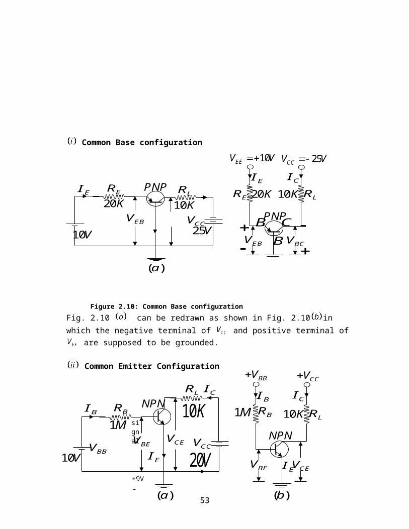
Figure 3.6: Op-amps as summing amplifier
Thus is the sum of the three inputs with each input multiplied by a factor , , is the corresponding input resistance. The minus sign for V0 indicates that V0
is anti-phase to the inputs. This result applies to ac and dc voltages and is quite useful for a microphone mixture since we do not want one microphone to affect another.
Activity 3.2.5: Positive Feedback, Square Wave Oscillator or A stable Multivibrator.
You have already learnt that:1. Negative feedback reduces the differential voltage at the input. 2. Likewise +ve feedback tends to increase the differential voltage at the
input since output voltage will be in phase with input voltage. 3. Thus the output quickly reaches saturation voltage. VS. If the Opamp
circuit is designed to make the output switch continually from +VS to –VS and from –VS to +VS an oscillating output voltage is obtained.
A circuit with positive feedback which produces square wave oscillations and acts as a stable multivibrator is shown in Fig. 3.7.
53
x
5R
4R
outV
_3R
2R1R
3V2V1V
0V2V1V
2R3R
1C
_1R
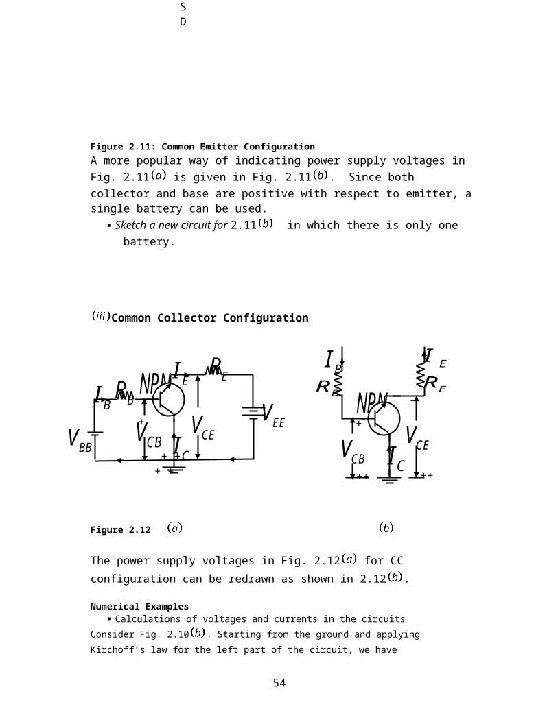
Figure 3.7: Positive Feedback, Square Wave Oscillator or A stable Multivibrator.
Action of the circuit.
Description of what takes place Read through and follow the explanation provided:
Let initially be uncharged and has its maximum positive value (+ V) due to a small differential voltage at the inputs.
A fraction of is fed back to the + input. Whereby
.
is also fed back to the – input through . This causes (which is initially uncharged) to charge up through towards +V and rises exponentially with time. As shown in Fig. 3.8
(a)
(b)
Figure 3.8: Variation of voltage with time
After a time which depends on the time constant reaches a value higher than ; & the output switches over so that the output is –V as shown in Fig. 3.8
54
Volta
ge
Time
Periodic time
Time
Volta
ge
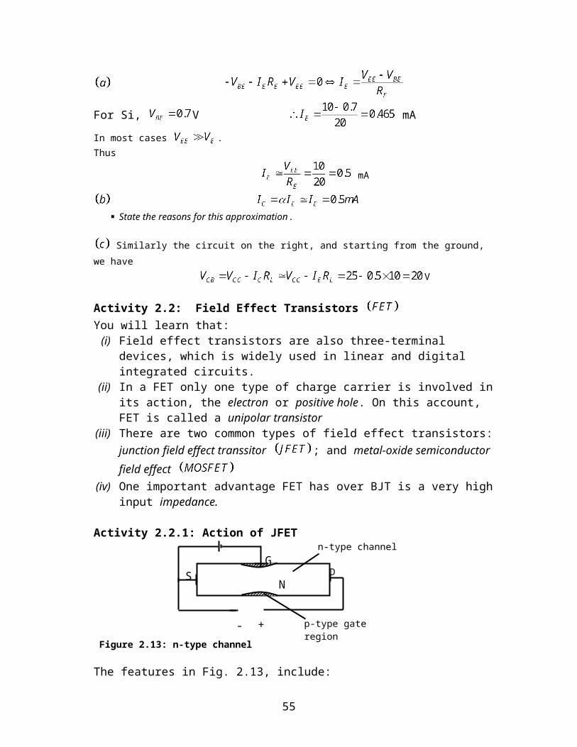
The positive feedback encourages the op-amp to switch quickly since then drops, making it much lower than and so forcing to go negative even more quickly. C1 now discharges (and starts to discharge in the opposite direction) until
becomes lower than . The op-amp then switches back again so that becomes positive (+V) again. The cycle is then repeated.Fig 3.8 shows how varies with time, and Fig 3.8 shows how the output voltage varies with time. The periodic time of the multivibrator is given by
Task 3.3: Further reading and Note makingUse the available references and make notes on
1. Sine wave Oscillator: write out the expression for the output frequency2. Op-amp as Comparator, and switching Cicuit
Activity 3.2.6: Op-amp as an integrator
1. Under this section the action of an op-amp as an integrator is presented for you. Read through and make sure that you understand the description.
Figure 3.9: Op-amp as an integrator
The circuit in Fig. 3.9 provides an output, that is an integral of the input voltage, . Point X is a virtual earth. The p.d. across is and the p.d across, C is . But,
and
55
-1I 2I
XinV
0 V
C
0V
R
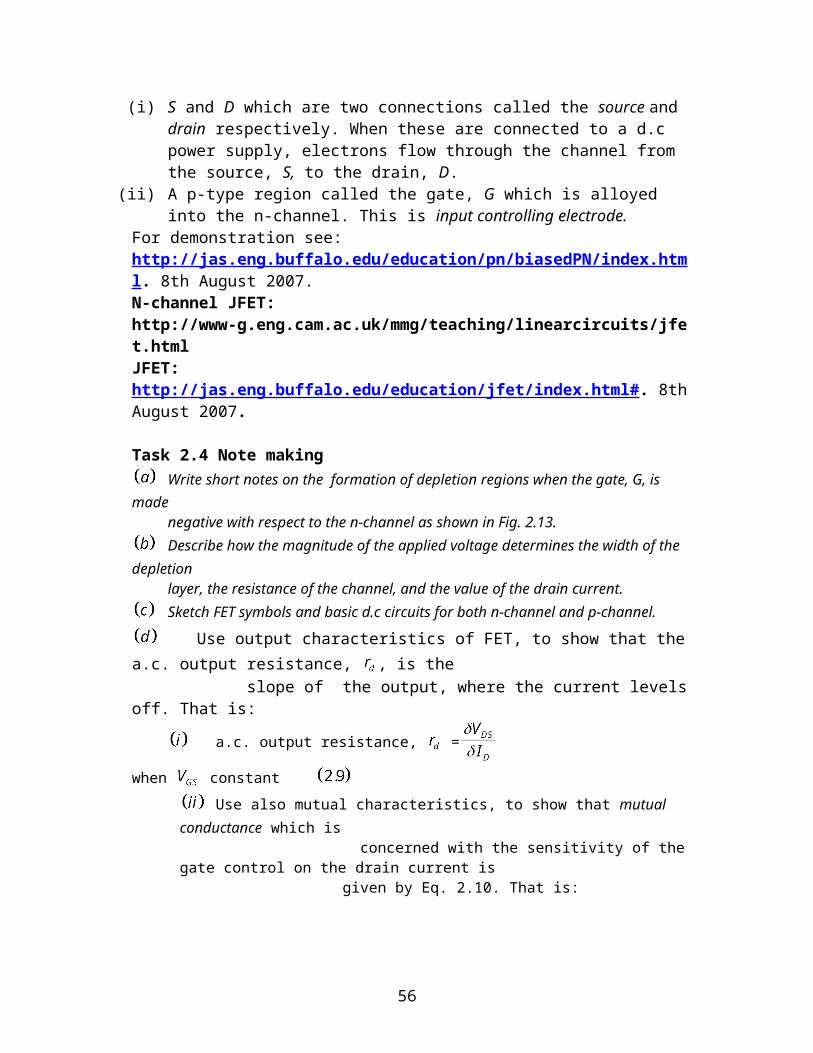
x
5R
3R
outV
_1R
2V1V
2R
At X,
Thus
the output voltage is proportional to the integral of the input voltage.From Eq. ,
(constant).
This means that varies linearly with time, t, and has a negative gradient.
SELF EVALUATION 3
1. List the factors which may lead to a specific op-amp being selected for use2. Calculate the output voltage in a non inverting amplifier for an input of 420 if
R1 = 1.7 k and .
3.
Calculate the output voltage for the circuit above, if mV and mV
56
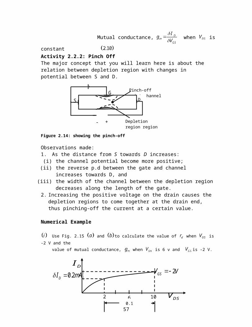
ACTIVITY 4: Digital Circuits
You will require 30 hours to complete this activity. Only basic guidelinesare provided to help you go through the activity.
Specific Teaching and Learning Objectives
In this activity you will be required to (i) Manipulate numbers in various bases (2,8,10,16)
(ii) Apply Boollean algebra in design of logic circuits and (iii) Design, analyse and synthesize logic circuits (multiplexer, decoders, Schmitt
triggers, flip-flops, registers) (iv) Explain the systems level components of a microprocessor
Summary of the learning activity
In this activity different number systems including decimal, binary, octal and hexadecimal Number System are learnt. In addition conversion from one system to another number systems, and how each number system is coded are considered. The last part of the activity is on Logic gates where characteristics of different logic gates are presented and discussed with suitable examples using Boolean algebra.
List of REQUIRED readings
Reading 1: Electronics WIKIBOOKSComplete Reference: http://en.wikibooks.org/wiki/Electronics. 5th October 2007.Abstract: Topics covered in this reading include: Analogue circuits, Digital circuits, Elements of Digital Circuits, Computer architecture, Analogue-to-Digital and Digital-to-Analogue converters.Rationale: The reading adequately covers the basic course of electronics outline in the activity.
Reading 2. Reference: http://en.wikipedia.org/wiki/electronics. 5th October 2007.Abstract: This reading is formed from references obtained from many sites. Their URLs can be obtained from a soft copy of this reading. Basically all the essential topics of the course are covered in this reading 2.Rationale. The reference provide easy reading sources on electronics that a reader should have no problem using them.
Reading 4: Boolean Algebra + Notes on Designing simulation of Schmitt’sTrigger circuitReference: http://en.wikipedia.org/wiki/Electronics/Boolean-Algebra. 5th October 2007.Rationale: This provides easy reading materials on Boolean Algebra.
57
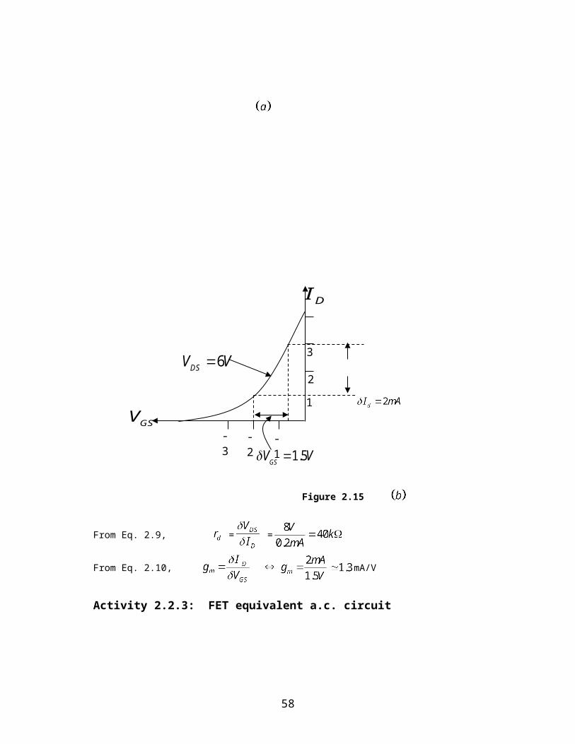
List of relevant MULTIMEDIA resources.
Reference: http://jas.eng.buffalo.edu/ 3rd October 2007.Summary: Useful illustration of amplifiers with BJT and MOSFET are used to promote easy understanding of the topics Rationale: Provides useful video about amplifiers with BJT or MOSFET -Circuit models of four basic amplifiers -Single-stage BJT amplifier circuits (CE, CB, and CC) -Single-stage common-emitter amplifier bias design (java1.1) -Single-stage MOSFET amplifier circuits (CS, CG and CD) -Different load types in an IC Amplifier Circuit (a CS amp example)
List of relevant useful links
Title: Digital Logic URL: http://www.educypedia.be/electronics/digital.htm. 3rd October 2007.Abstract: This site provides reading materials on logic gates, Venn diagrams, de Morgan's theorems, combinatorial logic circuits, canonical forms, Boolean algebra, Karnaugh maps, truth tables, switch debouncing, JK flip-flop, master-slave flip-flop, binary subtraction, binary arithmetic, JK Flip-Flop, D latch, D Flip-Flop, Flip-Flop symbols, converting Flip-Flop inputs, alternate flip-flop circuits, D Flip-Flop; using NOR latches, CMOS Flip-Flop construction, counters, ripple counter.
Title: Schmitt’s triggerURL: http://www.visionics.ee/curriculum/Experiments/Schmitt%20Trigger/Schmitt%20Trigger1.html. 3rd October 2007.Abstract: This provides additional reading on the theory of Schmitt’s trigger.
Title: Logic GatesURL: http://www.shef.ac.uk/physics/teaching/phy107/phy107.htmlhttp://www.shef.ac.uk/physics/teaching/phy107/phy107.html. 3rd October 2007.
Abstract: This reading equips the student with the fundamental skills required in digital circuit design. No prior knowledge of digital techniques is assumed. The reading first introduces the basic logic gates which form the fundamental building blocks of all digital circuits. It then progresses to combine these circuit elements in a number of ways in order build circuits which provide certain functionalities such as counting and addition. Aspects
of circuit design are also covered.
Title: Boolean AlgebraURL: "http://en.wikibooks.org/wiki/Electronics/Boolean_Algebra. 4th October 2007.Abstract: Here formal mathematical operations are presented along with Boolean
algebra laws. In addition, a number of examples are given.
Title: Multiplexing
58
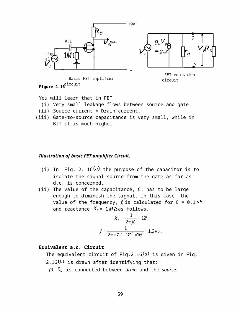
URL: "http://en.wikipedia.org/wiki/Multiplexing. 4th October 2007.Abstract: The reading includes telegraphy, video processing, digital broadcasting,
and analogue broadcasting.
Introduction
There are two basic types of circuits that may be considered as digital devices: Logic Gates, and Flip-flop. Electronic calculator is an example of a digital circuits, where information is processed in binary form, and the output are displayed as decimal numbers. The gradual turning of the potentiometer shaft is the analog input in a circuit consisting of a battery, potentiometer and ammeter all in series.
Examples of analog signals include: sine wave, audio and video signals, while the square wave is an example of a digital signal. A digital signal has two distinct amplitudes such as 0 and +5 V. The pulse is either all on or all off i.e. High or Low.
Activity 4.1.1 Number Systems
Manipulation of numbers in different basesActivity 4.1: Number systems:
A number system is a set of numbers, together with one or more operations, such as addition or multiplication.Examples of number systems include: natural numbers, integers, rational numbers, algebraic numbers, real numbers, complex numbers, p-adic numbers, surreal numbers, and hyperreal numbers.
NumeralThe numerals used when writing numbers with digits or symbols can be divided into two types that might be called the arithmetic numerals 0,1,2,3,4,5,6,7,8,9 and the geometric numerals 1,10,100,1000,10000... respectively.
There are four systems of arithmetic numerals which are often used in digital circuits. These systems are:
1. Decimal; it has a base (or radix) of 10 i.e. it uses 10 different symbols to represent numbers.
2. Binary; it has a base of two i.e. it uses only two different symbols.3. Octal; it has a base of 8 i.e. it uses eight different symbols.4. Hexadecimal; it has a base of 16, i.e. it uses sixteen different symbols.All these systems use the same type of positional notation except that a) decimal system which uses powers of 10 are used to represent quantities
which are outside the digital system. a. binary system which uses power of 2, is extensively used by digital
systems like digital computers which operate on binary information.b. octal system which uses power of 8, has certain advantages in digital
work because it requires less circuitry to get information into and out
59
of a digital system. Moreover, it is easier to read, record and print out octal numbers than binary numbers.
c. hexadecimal system which uses power of 16 is particularly suited for microcomputers
Activity 4.2: The decimal Number System. :
(i) Base or Radix The decimal number system has a base of 10 meaning that it contains ten unique symbols (or digits). These are: 0,1,2,3,4,5,6,7,8,9. Any one of these may be used in each position of the number.
(ii) Position Value Position value of a number 2573 given by:
2573 = 2*103 + 5*102 + 7*101 + 3*100
The number, 3 is the least significant digit (LSD) whereas 2 is the most significant digit (MSD). Again, the number 2573.469 can be written as
2573.469 = 2*103 +5*102 + 7*101 +3*100 +4*10-1 +6*10-2 +9*10-3
Activity 4.3: Binary Number SystemLike decimal number (or denary) system, it has a radix and it also uses the same type of position value system.
RadixIts base or radix is two because it uses only two digits 0 and 1 (the word ‘binary digit’ is contracted to bit). All binary numbers consist of a string of 0s and 1s. Examples are 10, 101, and 1011 which are read as one-zero, one-zero-one and one-zero-one-one. To avoid confusion subscripts of 10 for decimal and of 2 for binary are added as shown below.1010 , 10110 , 657410 ___ decimal number and
102 , 1012 , 1100012 ____ binary numbers.
Position ValueThe position value of each bit corresponds to some power of 2. A 7-bit binary number 1101.011 is as illustrated below MSD LSD
1 1 0 1 0 1 1
Binary PointThe decimal equivalent is
60
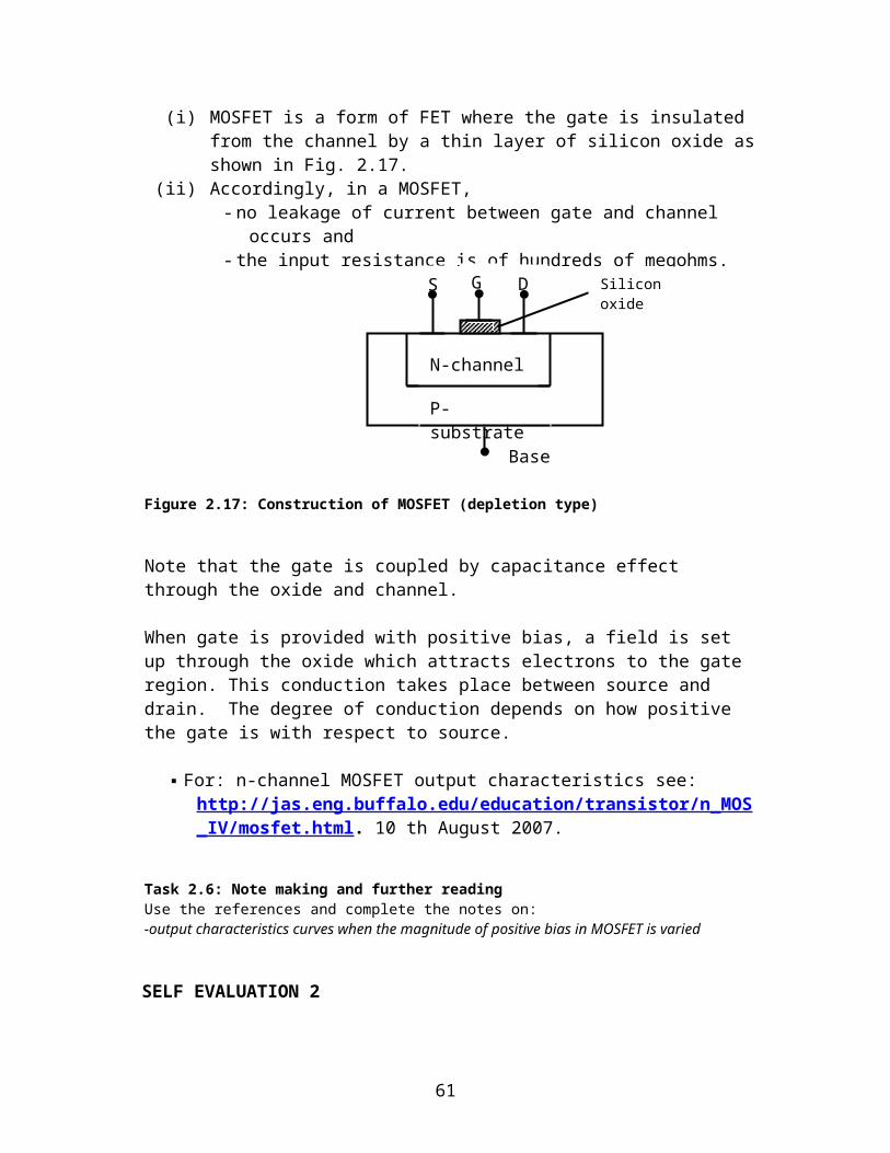
Binary numbers are used extensively by all digital systems primarily due to the nature of electronics itself. The bit 1 may be represented by a saturated (fully-conducting) transistor, a light turned ON, a relay energised or a magnet magnetized in a particular direction. The bit 0, on the other hand, can be represented as a cut-off transistor, a light turned OFF, a relay de-energised or a magnet magnetised in the opposite direction. In such cases, there are only two values which a device can assume.
Activity 4.4: Binary to Decimal Conversion The following procedures should be adopted for converting a given binary integer (whole number) into its equivalent decimal number:Step 1. Write the binary number i.e. all its bits in a row.Step 2. Directly under the bits, write 1, 2, 4, 8, 16, …… Starting from right to left.Step 3. Cross out the decimal weights which lie under the0 bits.Step 4. Add the remaining weights to get the decimal equivalent.
Example 4.1 Convert 11012 to its equivalent decimal number
Solution The four steps involved in the conversion are given as follow.
Step 1. 1 1 0 0 1Step 2 16 8 4 2 1Step 3 16 8 4 2 1
Step 4 16+8+1 = 25.
Activity 4.5: Binary FractionsThe procedure is the same as binary integers except that the following weights are used for different bit positions.
Example 4.2. Convert the binary fraction 0.101 into its decimal equivalent.
Solution. The following four steps will be used for this purpose. Step 1. 0 1 0 1Step 2. ½ ¼ 1/8Step 3. ½ ¼ 1/8Step 4. ½ +1/8 = 0.625
Example 4.3. Find the decimal equivalent of the 6-bit binary number 101.1012
Solution
61
1 0 1 1 0 14 2 1 ½ ¼ 1/84 2 1 ½ ¼ 1/8
= 5 + ½ +1/8 = 5.625
Activity 4.6: Double-Dadd Method This method of converting binary integers into decimal equivalents is much simpler and quicker than the method so far given especially in the case of large numbers. The three steps are involved:1. Double the first bit to the extreme left and add this doubled value to the next bit on
the right.2. Double the sum obtained and add the doubled value to the next bit.3. Continue step 2 until the last bit has been added to the previously-doubled sum.The conversion of 110012 is as follows. It is seen that 110012 =2510
1 1 0 0 1
Using double-dadd method, let us convert into its binary equivalent.
1. , add next bit 1 so that 2+1 =32. , add next bit 1 so that 6+1 =73. , add next bit 0 so that 14+0 =144. , add next bit 1 so that 28+1 =295. , add next bit 0 so that 58+0 =58
Therefore 1110102 = 5810 .
4.7. Decimal to Binary Conversion(a) IntegersSuch conversions can be achieved by using the so-called double-dadded method. Or by divide-by-two methods. As an example, let us convert 2510 into its binary equivalent.
25 ÷ 2 =12+ remainder of 1 TOP12 ÷ 2 = 6 + remainder of 06 ÷ 2 = 3 + remainder of 03 ÷ 2 = 1 + remainder of 11 ÷ 2 = 0 + remainder of 1 BOTTOM
Therefore 2510 = 110012
(b) Fractions
62
In this case, Multiply-by-two rule is used we multiply each bit by 2 and record the carry in the integer position.. The steps below shows how 0.812510 is converted into its binary equivalent.
0.8125 2 = 1.625 = 0.625 with a carry of 1 0.625 2 = 1.25 = 0.25 with a carry of 1 0.25 2 = 0.5 = 0.5 with a carry of 0 0.5 2 = 1.5 = 0.0 with a carry of 1
0.8125 = 0.1101
Activity 4.9: Binary OperationsThe following four binary operations are considered:1. addition 2. subtraction 3. multiplication 4. division
Use your school knowledge of mathematics to carry out binary addition.
Binary subtraction. Binary subtraction requires more borrowing operations than decimal subtraction. The four rules for binary subtraction are provided as follows:
1. 0 – 0 = 0, 2. 1 - 0 = 1, 3. 1 – 1 = 0,4. 0 – 1 = 1 with a borrow of 1 from the next column of the minuend or 10 – 1 = 1
Example 4.4 Let us subtract 01012 from 11102 . The various steps are explained below:
1110-0101 1001
Explanation1. In the first column, since we can not subtract 1 from 0, we borrow 1 from the next
column to the left. Hence, we put down 1 in the answer and change the 1 of the next left column to a 0.
2. We apply Rule 1 to the next column i.e. 0 – 0 = 0.3. We apply Rule 3 to the third column i.e. 1 – 1 = 0.4. Finally, we apply Rule 2 to the last i.e. fourth column it. 1 – 0 = 1
As a check, it may be noted that talking in terms of decimal numbers, we have subtracted 5 from 14. Obviously, the answer has to be 9 (10012).
Activity 4.10: Complement of a Number.In digital work, two types of compliments of binary number are used for complemental subtraction:
63
(a) 1’s complementThe 1’s complement of a binary number is obtained by changing its each 0 into a 1 and each 1 into a 0. It is also called radix-minus-one-complement. For example, 1’s complement of 1002 is 0112 and of 11102 is 00012.
(b) 2’s complementThe 2’s complement of a binary number is obtained by adding 1 to its 1’s complement.
2’s complement = 1’s complement + 1 This is also known as true complement.
Example: 4.5
The 2’s complement of 10112 is found as follows:Step 1: Its 1’s complement is 0100 .
Step 2: Add 1 to 0100 in order to get 01012.
Step 3: Thus, 2’s complement of 1011 is 0101 .The complement method of subtraction reduces subtraction to an addition process.In digital computers this method is popular because
1. Only adder circuits are needed thus simplifying the circuitry.2. It is easy with digital circuits to get the complements.
Activity 4.10: 1’s Complemental Subtraction.Subtracting of a number is done by adding its 1’s complement to the minuend, using the following rules:
1. Compute the 1’s complement of the subtrahend by changing all its 1s to 0s and all its 0s to 1s..
2. Add this complement to the minuend.3. Perform the end-around carry of the last 1 or 0.4. If there is no end-around carry (i.e. 0 carry), then the answer must be
recomplemented and a negative sign attached to it.5. No recomplementing is necessary if the end-around carry is 1.
Example 4.6:Subtracting 101 from 111 is performed as follows:
Solution111
+ 010 1’s complement of subtrahend 101 1001
1 end-round carry010
The final answer is obtained by removing from the addition sum carry in the last position and added it onto the remainder. This is called end-round carry.Task 4.1: Using the rules stated under 4.13 in solving problems
Use the rules for subtraction and carry out the following subtractions.
64
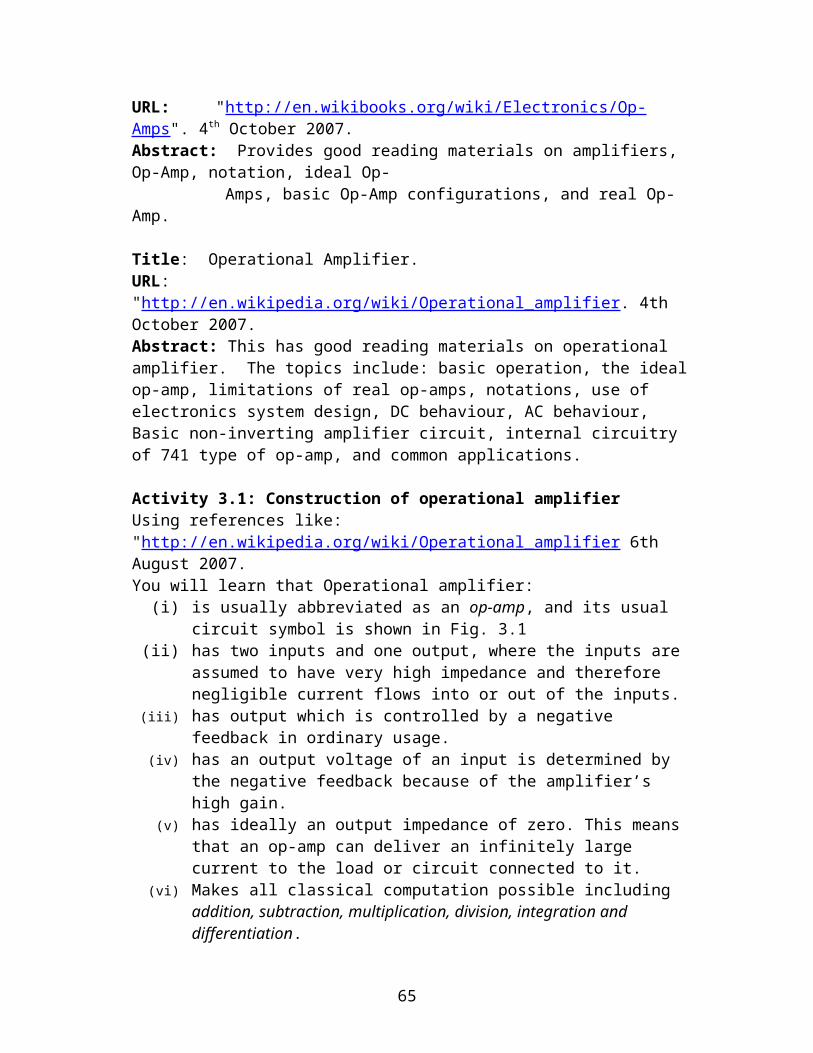
a. Subtract 1101 from 1010 . The final answer is -0011. Explain how this is obtained.
b. Subtract 1110 from 0110 . The answer is -1000 .
c. Subtract 01101 from 11011 . The answer is 01110 .
Activity 4.11: 2’s Complemental SubtractionThe essential steps are given as follows:
1. Find the 2’s complement of the subtrahend,2. Add this complement to the minuend,3. Drop the final carry,4. If the carry is 1, the answer is positive and needs no recomplementing, 5. Recomplement the answer and attach minus sign if there is no carry.
Example 4.7: Using 2’s complemental subtraction
Subtract 1010 from 1101Solution.
The 1’s complement of 1010 is 0101The 2’s complement is 0101 + 1 = 0110Adding this to 1101 we get
1101 +0110 10011
Dropping the final carry gives the final answer as 0011 .
Activity 4.12: Binary Multiplication and DivisionThe procedure for multiplication and division are the same as for decimal multiplication and division. The four simple rules for multiplication are:i. 0 0 = 0, ii. 0 1 = 0, iii. 1 0 = 0, iv. 1 1 = 1.
Rules for division are:i. 0 1=0 ii. 1 1= 1 iii. Division of 1 by 0 is meaningless Task 4.2: Further Reading and note making
a) Use available references and read about multiplication and division of binary numbers.
b) Do as many examples as possible in order to come to grip with such problems.
c) Multiply 1101 by 1100 (Answer is 1001100 ).d) Multiply 111 by 111 (Answer is 101001 ).e) Divide 11001 by 101 (Answer is 101 ).f) Divide 110011 by 100 (Answer is 110.11 ).
Activity 4.13: Octal Number System. (i) Radix or Base
65
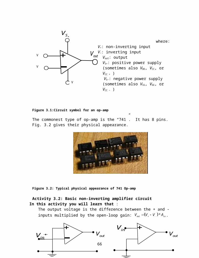
It has a base of 8 which means that it has eight distinct counting digits:0,1,2,3,4,5,6, and7
These digits 0 through 7 have exactly the same physical meaning as in decimal system. Beyond 7, the counting becomes
0, 1, 2, 3, 4, 5, 6, 7,10, 11, 12, 13, 14, 15, 16, 17,
20, 21, 22, 23, 24, 25, 26, 27, 30, 31, 32, … … … … …
(ii) Position valueThe position value (or weight) for each digit is given by different powers of 8 as shown below:
8 8 8 8 8 8 8
octal pointExample 4.8: Conversion of octal numbers to decimal453
453.27
Example 4.9: Conversion of decimal numbers to octalHere 8 acts as a multiplying factor for integers and as a dividing factor for fractions.256
with 0 remainderwith 0 remainderwith 4 remainder
Similarly, is worked out as follows
with a carry 3with a carry 3with a carry 4with a carry 1with a carri 1 etc.
.
Activity 4.14: Binary to Octal Conversion
66
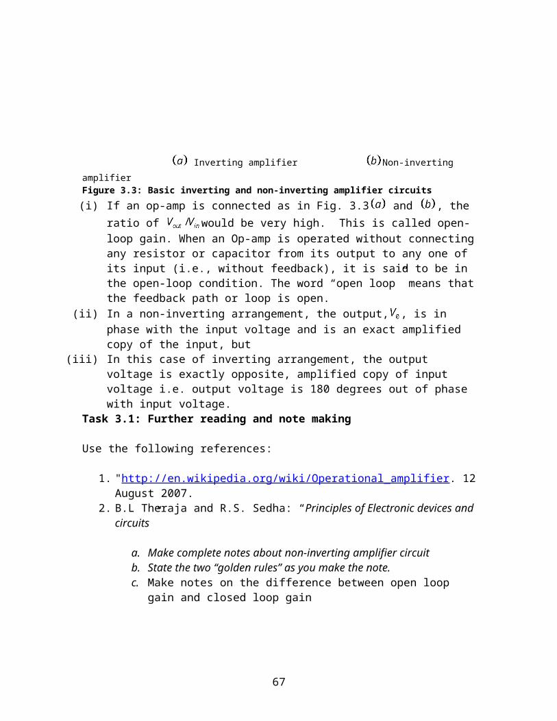
The simplest procedure is to use the binary-triplet method, where the given binary number is arranged into groups of 3 bits starting from the binary point and then each group is converted to its equivalent octal number.
Example 4.10 convert 101011 into its octal equivalent.
SolutionStep 1: Start by converting the bits into groups of three, i.e.
101011 101 011Step 2: Convert each of these into octal
101 is 5 octal and 011 is 3 octal.
5 3
Convert 1101.11 into octal
SolutionStep 1. Group the bits into three i.e
1101.11 001 101 110Step 2
1 5 6
Activity 4.14.1: Usefulness of Octal Number System.The ease with which conversions can be made between octal and binary makes the octal system attractive as a ‘’shorthand’’ means of expressing large binary numbers. It should be noted that some binary numbers, in computers do not always represent a numerical quantity but are often some type of code that conveys non numerical information, like
(i) actual numerical data,(ii) numbers corresponding to a location called (address) in memory,
(iii) an instruction code,(iv) a code representing alphabetic and other non numerical characters,(v) group of bits representing the status of devices internal or external to the
computer.It is convenient and more efficient to write a number in octal rather than binary when dealing with a large quantity of binary numbers of many bits. But, remember that the digital circuits and systems work strictly in binary.
Activity 4.15. Hexadecimal Number System.Hexadecimal Number System
1. It has a base of 16 and therefore, it uses sixteen distinct counting digits 0 through 9 and A through F as follows: 0,1,2,3,4,5,6,7,8,9,A,B,C,D,E,F
2. Place value for each digit is in ascending powers of 16 for integers and descending for powers of 16 for fractions.
67
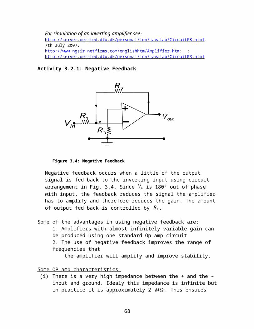
This system is used for specifying addresses of different binary numbers stored in computer memory.
Example 4.11: Counting beyond F………F 10 11 12 13 14 15 16 17 18 19 1A 1B 1C 1D 1E 1F 20 21 22….
Activity 4.16: Digital Coding
In digital logic circuits, each number or piece of information is represented by an equivalent combination of binary digits called digital code.The usefulness of a code among others is to
(i) Reduce on the circuitry requirement.(ii) Increases on the reliability of digital system.
(iii) Allows for error detected to be corrected.
Activity 4.16.1: Binary Coded Decimal (BCD) code
Binary Coded Decimal (BCD) code is used to represent a decimal digit by a group of four bits. From right-to-left the weighting of the 4-bit positions is 8-4-2-1 This is also called 8421 code. It is a weighted numerical code. Each decimal digit from 0 through 9 requires a 4-bit binary-coded number as shown in Table 4.1
Table 4.1
Decimal BCD0 00001 00012 00103 00114 01005 01016 01107 01118 10009 1001
a) However, any decimal number is expressed in BCD code by replacing each decimal digit by the appropriate 4-bit combination.
b) Conversely, a BCD number is converted into a decimal number by dividing the coded number into groups of four bits (starting with LSB) and then writing down the decimal digit represented by each four-bit group.
Example 4.12: Write the decimal number 674 in BCD code.
Solution. 0110 0111 0100.Similarly, the BCD codes for the following decimal numbers are shown in Table 4.2.
68
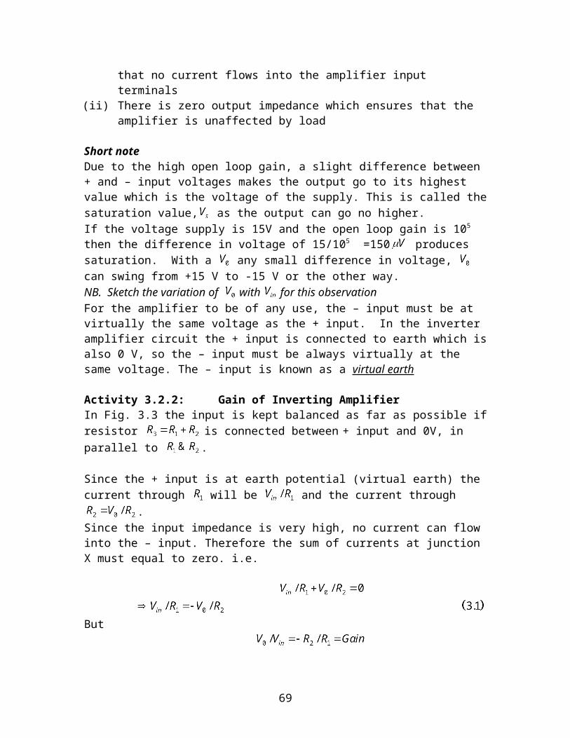
Table 4.2
Decimal BCD51 0101 0001428 0100 0010 10007369 0111 0011 0110 100121057 0010 0001 0000 0101 0111
Activity 4.16.3: Octal Coding.It involves grouping the bits in three’s. For example, (2341)8 = (010 011 100 001)2 = (010011100001)2. Similarly, the 24-bit number stored in the computer memory such as 110 010 101 001 010 111 000 011 can be read in the octal as
110 010 101 001 010 111 000 011
6 2 5 1 2 7 0 3
Activity 4.16.4: Hexadecimal Coding.The advantage of this coding is that four bits are expressed by a single character. However, the disadvantage is that new symbols have to be used to represent the values from 1010 to 1111 binary.
LOGIC GATES
Activity 4.17: Definition of a logic gateA logic gate is an electronic circuit which
(i) makes logic decisions based on certain combinations of input signals. (ii) has one output and one or more inputs.
(iii) implement the hardware logic function based on Boolean algebra. The variables used in Boolean algebra is either a 0 or a 1. The commonest ICs of these gates are: transistor-transistor logic (TTL), emitter-coupled logic (ECL), metal-oxide semiconductor (MOS), and complementary metal-oxide-semiconductor. (CMOS).
For demonstration see the following Useful Applets: http://jas.eng.buffalo.edu/CMOS Inverter Gate Applet: http://jas.eng.buffalo.edu/education/mos/inverter/index2.html: 4th October 2007.
Analog Switch & Transmission Gate: http://jas.eng.buffalo.edu/education/mos/tgate/index.html. 4th October 2007.
Activity 4.17.1: Positive and Negative Logic The number symbols 0 and 1 represent possible states of a circuit or device in computing systems where we can have a positive logic or negative logic. In a positive logic, a 1
69
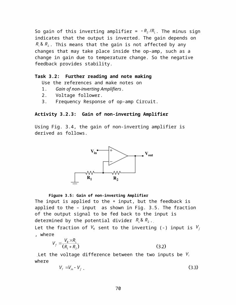
represents either: an ON circuit, a CLOSED switch, a HIGH voltage, a PLUS sign, or a TRUE statement. On the other hand a 0 represents either: an OFF circuit, an OPEN switch, a LOW voltage, a MINUS sign, or a FALSE statement. In a negative logic, just opposite conditions prevail.
For a digital system with two voltage levels 0V and 5V, we have a positive logic system if the symbol 1 stands for 5V and symbol 0 for 0V. But if one makes a 1 to represent 0V and 0 to represent 5V, then we will get negative logic system.
Basically, the more positive of the two voltage levels represent the 1 while in negative logic, the more negative voltage represents the 1, and it is not essential that a 0 has to be represented by 0V.
Activity 4.17.2: The OR GateThis activity requires you to learn that
The symbol for a two-input OR gate with its inputs marked as A and B and the output as X is as shown in Fig 4.1 (a). Its equivalent switching circuit is shown in Fig 4.1 (b). The three variables A, B and X can have either 1 or 0 only at a time.
AX
BA + B = X
Figure 4.1: The OR Gate
Activity 4.17.3: Logic operation.
The key learning points are:a) The OR gate has an output of 1 when either A or B or BOTH are 1.b) That is, it is an any-or-all gate because an output occurs when any or
all the inputs are present. c) In Fig.4.1 (b), the lamp will light up (logic 1) when either switch A or
B or both are closed.
But, the output is 0 if and only if both inputs are 0. In switching conditions, the lamp is OFF (logic 0) only when both switches A and B are OFF.
The OR gate represents the Boolean equation A + B = X. In Eq. 4.1, X is true when either A is true or B is true or both are true. Alternatively, it means that output X is 1 when either A or B or both are 1. The OR gate in this case is called inclusive OR gate because it includes the case when both inputs are true. The ‘+’ sign in Eq. 4.1 indicates OR operation and not that the sum of A and B equals X. The other symbols used instead of ‘+’ are U and V. Thus, Eq. 4.1 can also be written as:
AUB = X or AVB = X.Example 4.13: Transistor OR Gate
70
X
AB
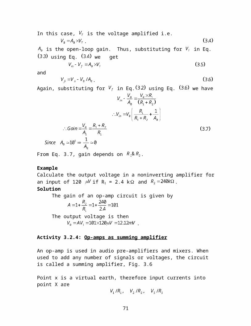
MN
3Q2Q1QA
1R 2R5V
X B
This example, illustrates a possible transistor OR gate consisting of three interconnected transistors Q1, Q2, and Q3 supplied from a common supply = +5V as shown in Fig 4.3.
Figure 4.2: Transistor OR Gate consisting of three interconnected transistorsDescription of what takes place in Fig.4.2
(i) When +5V is applied to A, Q1 is forward-biased and so it conducts. Assuming that is
saturated, entire = 5V drops across thus causing N to go to ground. This, in turn, cuts off
thereby causing X to go to i.e. +5V.
(ii) When +5V is applied to B, conducts thereby driving N to ground i.e. 0V. With no forward
bias on its base, is cut-off thus driving X again to i.e. +5V.
(iii) If both inputs A and B are grounded and are cut-off driving N to +5V. As a result,
becomes forward-biased and conducts fully. In that case, entire drops across driving M and hence X to ground.
Task 4.3: Construction of a Truth table for the OR gate. For all possible input combinations, use Fig.4.1 and construct a truth table which gives the output
state. Explain the meaning of each combination. Construct a truth table for a three input OR gate
Activity 4.17.4: Exclusive OR GateIn this section you will learn that:
a) The symbol for Exclusive OR Gate is as shown in Fig. 4.3 (a) and its equivalent switching circuit in Fig 4.3 (b).
b) In this type of gate, the output is 1 when its inputs are different and the output is 0 when both inputs are the same.
c) The circuit is also called an equality comparator or detector because it produces an output only when the two inputs are different.
: Exclusive OR Gate : Equivalent switching circuit
Figure 4.3: Here we deal only with exclusive statements such as:
You can be rich OR you can be poor,
71
VoltageVoltage
Voltage
VoltageVoltage
VoltageVoltage
VoltageVoltage
Time
Periodic time
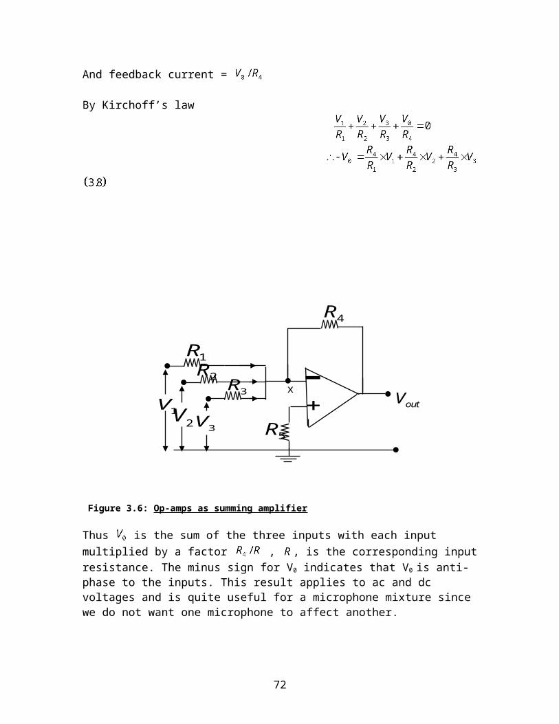
lampX
AB
Obviously, you can not be both at the same time.The change-over switching circuit of Fig 4.3 (b) simulates the exclusive OR (XOR) gate. Switch positions A and B will individually light up the lamp but a combination of A and B is not possible. You may construct the truth table.
Activity 4.17.5: The AND Gate The logic symbol for a 2-input AND gate is shown in Fig 4.4 (a) and its equivalent switching circuit in Fig 4.4 (b). Each of the three variables A, B, X can have a value of either 0 or 1.
Figure 4.4: 2-input AND gate Equivalent switching circuit Logic operation.
The AND gate gives an output only when all its inputs are present. The AND gate has a 1 output when both A and B are 1. Hence, this gate is an all-
or-nothing gate whose output occurs only when all its inputs are present. In true / false terminology, the output of an AND gate will be true only if all its
inputs are true. Its output would be false if any of its inputs is false.The AND gate works on the Boolean algebra .
This is different from the arithmetic multiplication. The logical meaning of Eq. is that
output X is 1 only when both A and B are 1. output X is true only when both A and B are true.
Task 4.4: construction of a truth tableConstruct a truth table for a 2-input AND gate.
Construct a truth table for a 3-input AND gate.
Design the equivalent electrical circuits for the AND gate.
Activity 4.17.6: AND Gates Symbolizes Logic Multiplication. According to Boolean algebra, the AND gate performs logical multiplication on its inputs according to Eq. 4.4.
0.0 = 0 , 1.0 = 00.1 = 0, 1.1 = 1
In general, the Boolean laws of multiplication are given by Eq. :A.1 = A, A.0 = 0
72
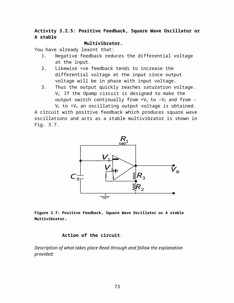
XBA
A.A = A
Activity 4.17.7: The NOT Gate
The output for this gate is NOT the same as its input. This gate is also called an inverter because it inverts the input signal. It has one input and one output as shown in Fig 4.5(a) and the truth table is shown in Fig. 4.5 (b). The schematic symbol for inversion is a small circle as shown in Fig. 4.5 (a).
The symbol for inversion or negation or complementation is a bar over the function to indicate the opposite state. For example, means not-A. Similarly, means the
complement of .
The NOT OperationThis is a complementation operation and its symbol is an overbar. For example Thus, the double complementation gives the original value.
Activity 4.17.8: The NOR Gate. This is a NOT-OR gate that can be made out of an OR gate by connecting an inverter in its output as shown in Fig 4.6 (a).
Figure 4.6: A NOT-OR gate that can be made out of an OR gate
The output equation is given by
A NOR function is just the reverse of the OR function.
Task 4.5: Equivalent Circuits for a NOT Gate.
A B01
10
73
Time
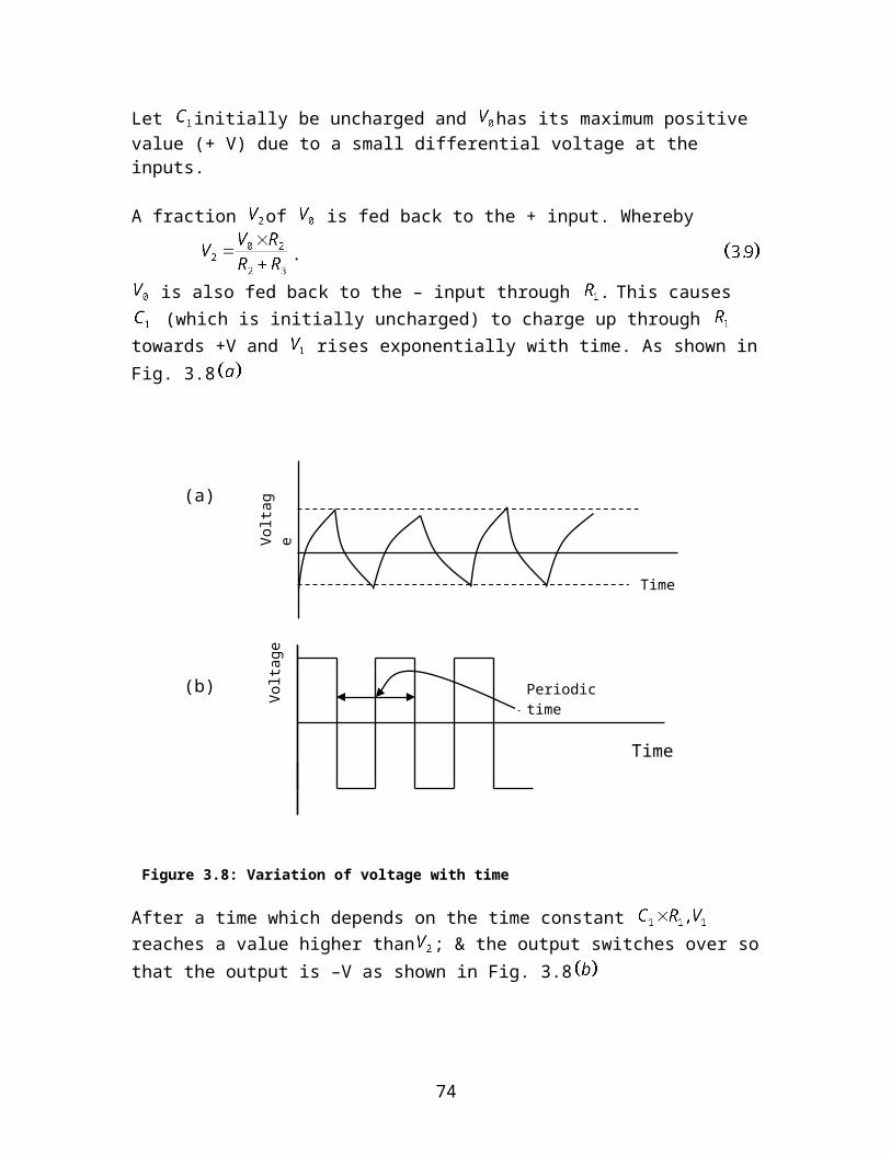
As OR gate
X AB
A
B BA X A B A B
BA
=AAA
a b
c
As AND gate
As NOT gate
NOR Gate is a Universal GateA NOR gate is often referred to as a universal gate because it can be used to realize the basic logic functions: OR, AND and NOT.
Figure 4.7:
As OR Gate
In Fig.4.7 the output from NOR gates is A + B. By using another inverter in the output, the final output is inverted and is given by X = A + B which is the logic function of a normal OR gate.
As AND GateIn order to use a NOR gate as an AND gate, two invertors are used, one for each input as shown Fig 4.7 .
As NOT Gate
As a NOT gate, the two inputs are connected together as shown in Fig. 4.7 . The output is .
Activity 4.17.8: The NAND GateThe NAND Gate is a NOT-AND gate. It can be obtained by connecting a NOT gate in the output of an AND gate as shown in Fig 4.8. Its output is given by the Boolean equation.
74
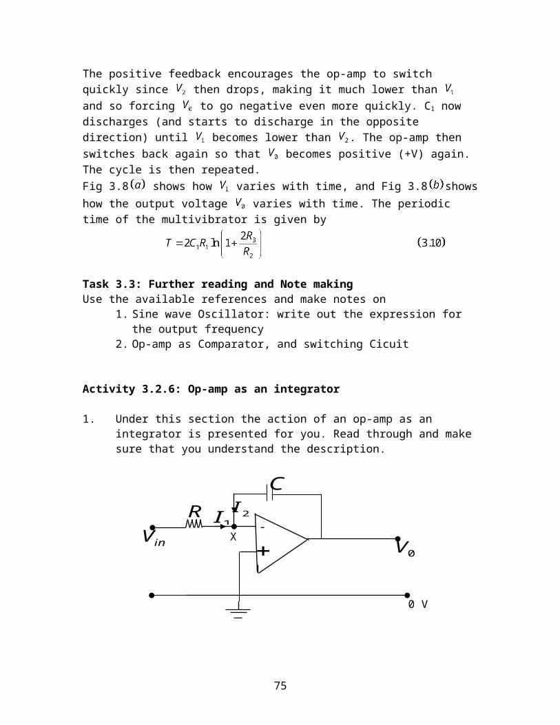
X X ABAB
AB
a b
00
110101
00 1 1 output signal
input signal
Figure 4.8
If both inputs are not 1, then the output of the gate will be 1.
NAND Gate is a universal Gate.NAND gate is called universal gate because it can perform all the three logic functions of an OR gate, AND gate and inverter.
Task 4.6: Further Reading and Note Making Show how a NOT gate can be made out of a NAND gate.
Show how you can use two NAND gates to produce an AND gate.
Show how an OR gate can be made out of three NAND gates.Example 1: An electrical signal is expressed as 101011. Explain its meaning. If this signal is applied
to a NOT gate, what would be the output signal?Solution
The binary number for the input signal is represented as a train of of pulses. The positive logic, 1
represents high voltage and 0 represents low. The binary number for the output signal is
Example 2. Two electrical signals represented by A = 101101 and B =110101 are applied to 2-input AND gate. Sketch the output signal and the binary number it represents.
Solution. The pulse trains corresponding to A and B are shown in Fig 4.9. In an AND gate, C is 1 only when both A and B are 1.
75
01 011
00
1
0 0 1111
A
B
1 0 11C output signal
input signal
input signal
1 2 3 4 5 6 Time intervals
Combinational outputs
Combinational Logic gates
External inputs
Figure 4.9. Showing input signals A, and B, and output signal C
The output can be found in different time intervals as follows:
1. 1st interval : 1 + 1 = 12. 2nd interval : 0 + 1 = 03. 3rd interval : 1 + 0 = 04. 4th interval : 1 + 1 = 15. 5th interval : 0 + 0 = 06. 6th interval : 1 + 1 = 1
Hence, output of the AND gate is .
Activity 4.17.8: Combinational Logic Circuit.
Combinational logic circuit is a circuit built from various logic gate combinations. The circuit possesses a set of inputs, a memoryless logic network to operate on the inputs and a set of outputs as shown in Fig. 4.10. The output from a combinational logic circuit depends solely on the present input value and not on the previous ones.. Examples of such a circuit are: decoders, adders, multiplexer and demultiplexer etc.
76
F2c1c
3coutput
Address
0C1C
1nC
1-4multiplexer
input
A Bselect
output
Figure 4.10: Combinational Logic Circuit
Activity 4.17.9: Multiplexer and DemultiplexerThe multiplexer (MUX) is a device which selects only one input out of N input data sources, under the influence of a select input, shown in Fig.4.11 . It has a single output line. Thus the multiplexer is a combinational logic switch which is controlled by a logical signal.
(a) (b)Figure 4.11 (a) Mechanical analogue of multiplexer; 4 to 1 multiplexer, (b) Block diagram
Demultiplexer
A demultiplexer performs the inverse process of a multiplexer. It can take one input and transfer the data on that input line to the correct one of several output lines, under the influence of a select input.
Use standard electronic textbooks and compile notes on the working of a demultiplexer.
Activity 4.17.11: Flip-Flops
The name flip-flop describes the ability of a circuit to change between two stable states. A flip-flop, which is also called a bi-stable multi-vibrator, constitutes a basic digital memory circuit because it has two stable states. One of the stable states is known as SET or logic 1, and the other stable state is called RESET, CLEAR or 0.
Most flip-flops are of the clocked type, in which the change of flip-flop state takes place at some definite rate. Some of the most widely used flip-flops are of SR, JK, D and T types
77
QR
S
SR-flip-flop. The simplest type of flip-flop is the set-reset or S-R flip-flop. It has two inputs: the S and R inputs and the two outputs, which are complementary to each other, denoted by and . The SR-flip-flop circuit is sometimes called SR-latch. The latching means the circuit maintains one condition, in the disabled mode, until it is released by an S or R pulse. The construction of SR latch is shown in Fig. 4.12.
Figure 4.12: SR Flip-flop circuit with two NOR gates
There are four modes of operation: (i) disabled or inhibited mode, (ii) set mode (iii) reset or clear mode and (iv) prohibited or not allowed mode.
Activity 4.19: BOOLEAN ALGEBRA
4.18.1: IntroductionBoolean Algebra is not the ordinary numerical algebra we know from high schools but a totally new system called logic algebra.As already seen before, Boolean algebra is ideal for the design and analysis of logic circuits used in computers. It provides an economical and straight forward way of describing computer circuitry and complicated switching circuits. As compared to other mathematical tools of analysis and design, Boolean algebra has the advantages of simplicity, speed and accuracy.
4.18.2: Unique Feature of Boolean Algebra. Unlike in ordinay algebra, the variables used in Boolean algebra have a unique
property i.e. they can assume only one of the two possible values of 0 and 1. Each of the values used in a logical or Boolean equation can assume only the value of 0 or 1. For example, in the logical equation A + B = C, each of the three variables A, B and C can have only the value of either 0 or 1.
4.18.3: Laws of Boolean AlgebraBoolean algebra is a system of Mathematics based on logic. It has its own set of fundamental laws which are necessary for manipulating different Boolean expressions.
1. OR Laws
78
Law 1. Law 3.Law 2. Law 4.
2. AND LawsLaw 5. Law 7.Law 6 Law 8.
3. Laws of complementationLaw 9. Law 12. If A = 0, then Law10. Law 13.Law 11. If A = 0, then
4. Commutative laws These laws allow change in the position of variables in OR and AND expressions.
Law 14. A+ B = B + A Law 15. A.B = B.A
Laws 14 & 15 means that the order in which a combination of terms is performed does not affect the final result of the combination.
5. Associative lawsThese laws allow removal of brackets from logical expression and regrouping of variables.
Law 16.
Law 17.
Law 18.
6. Distributive LawsThese laws permit factoring or multiplying out of an expression. Law 19. .
Law 20. . Law 21. .
7. Absorptive Laws
These enable us to reduce a complicated logic expression to a simpler form by absorbing some of the terms into existing terms.
Law 22. Law 23.
Law 24. .
SELF EVALUATION 4
1. Convert the binary fraction 0.111 into its decimal equivalent.
79
X
AB
C
2 Convert into its binary equivalent.
3. Convert 25.625 into its binary equivalent. 4. In the following conversions, comment on the answers that you get i - 1101.0 and 11010.0 .
ii- 1101.0 and 110.10 .5. Carry out the following binary subtraction
a. 1000 - 0001 .
b. 1001 - 0111 .
c. 1101 - 1010 .6. Express the following hexadecimal numbers as binary numbers
D8 4E.7. (a) Use references to a draw equivalent circuits for a NOT Gate and explain how the circuit works.
(b)
Find the Boolean equation for the output X.
Evaluate X when: A = 0, B = 1, C = 1 , and when A = 1, B = 1, C = 1 (c) Construct a logic operation for a NOR gate and explain how it works8. i) Draw the logic circuit for the multiplexer shown in Fig. 4.11
ii) Write the logic equation which provides the switching function.iii) The demultiplexer performs the inverse process of a multiplexer. Write a
short note on it.9. Construct a Truth table for Fig. 4.13
Use Fig. 4.13 to describe how the four modes of operation: disabled or inhibited mode; set mode; reset or clear mode; and prohibited or not allowed mode that can be obtained.
Draw a Clocked SR-Flip flop circuit and describe its mode of operations.
80
ACTIVITY 5: Data Acquisition and Processes Control
You will require 20 hours to complete this activity. Only basic guidelinesare provided to help you go through the activity.
Specific Teaching and Learning Objectives
In this activity you will be required to: (i) Explain the operation of a transducer in various modes (strain, light, piezo,
temp)(ii) Explain and apply transducer signal conditioning processes and
(iii) Apply conditioned signal in digital form
Summary of the learning activity
In this activity, different types of transducers are considered in relation to how processing of information is done. The discussion on processing of information is in three parts: sensors, signal conditioning, and data acquisition. As an example of sensors, piezoelectric sensor is discussed and expression for voltage generated is derived. Under signal conditioning some of the following are discussed: requirements for analogue-digital converters; signal isolation, signal processing; removal of undesired signals. In addition, coversions of sensor voltage, current, and resistance to voltage are discussed. The last section of the activity considers data acquisition where the topics
81
discussed include anti-aliasing; sample and hold; analogue to digital conversion; and system integrations. In some instances, some equations are derived and used for numerical problems.
List of REQUIRED readings
Reading 1 WIKIBOOKS.
Complete reference: http://en.wikibooks.org/wiki/Electronics/Boolean_Algebra. 5th October 2007.Abstract: Topics covered include among others: formal mathematical operators, Boolean algebra laws (Associativity, distributivity and commutivity).Rationale. This provides basic reading materials on Boolean Algebra.
Reading 5: Sensors.
Reference: http://Soundlab.cs.princeton.ed/learning/tutorials/sensors/node19.html. 7th July 2007.
Abstract: the topics included are data acquisition (piezoelectric sensors, accelerometer, force sensing resistors, microphones, biopotential sensors); Signal conditioning (Requirements for A-D converters, voltage to voltage, current to voltage, resistance to voltage,, capacitance to voltage); data acquisition(anti aliasing, analogue to digital conversion, data acquisition systems).Rationale. This reading provides good materials on this activity.
List of relevant MULTIMEDIA resources
Reference: http://images.google.co.uk/images?hl=en&q=Transducers&oe=UTF-8&um=1&ie=UTF-8&sa=N&tab=wi. 4th October 2007.Summary: Images of different types of transducers are provided.Rationale: The resource is quite good as it provides one with information about the different transducers.
Reference: http://images.google.co.uk/images?hl=en&q=sensors&oe=UTF-8&um=1&ie=UTF-8&sa=N&tab=wi. 4th October 2007.
Summary: the resource provides different types of sensors.Rational: The images reinforces the learning when one looks at them.
List of Relevant Useful Links
Title: Piezoelectricity
URL: http://en.wikipedia.org/wiki/Piezoelectricity. 4th October 2007.
82
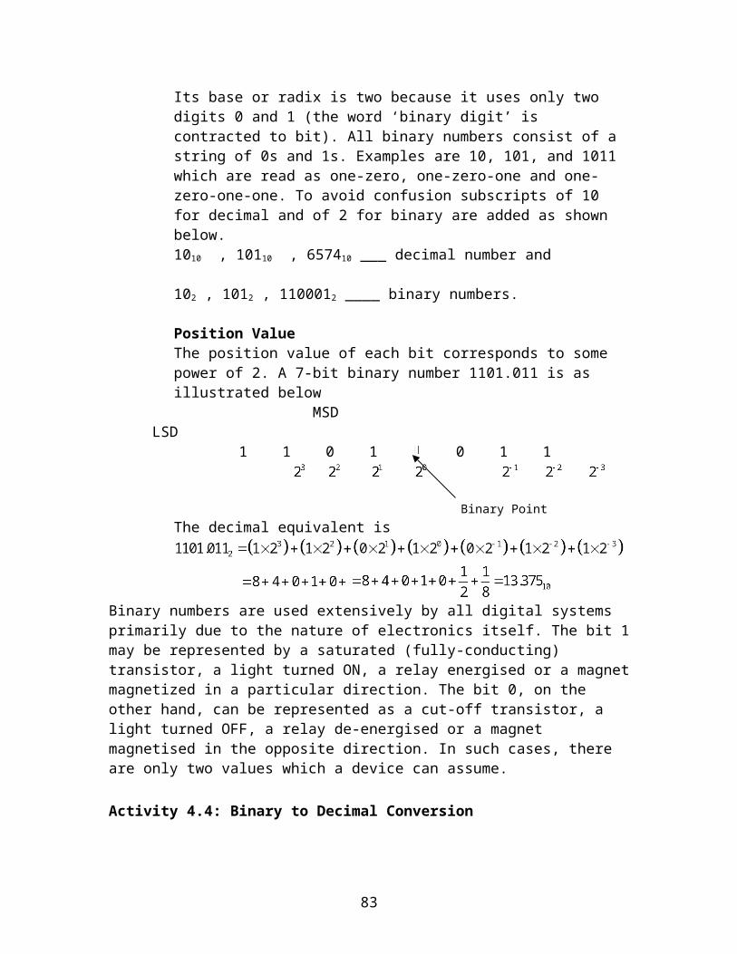
Abstract: This provides useful reading on : materials, applications which includes high voltage and power sources, sensors, actuators, piezoelectric motors, and crystal classes.
Title: Transducers URL:. "http://en.wikipedia.org/wiki/Transducer"; 4th October 2007. Abstract: This provides good reading about types of transducers, which include among
others: antenna, flourescent lamp, Hall effect sensor, rotary motor, vibration powered generator, piezoelectric crystal and photodiodes.
Activity 5.1: Operation of Transucers In this activity you will be required to:
(i) Explain the operation of a transducer in various modes.(ii) Explain and apply transducer signal conditioning processes.
(iii) Apply conditioned signal in digital form. Since electronics is a course which is not taught much at school, this activity will to a large extent provide you most of the basic information related to the different concepts. However, you will be required to carry out extensive reading in order to cover up the missing gaps. A number of references are given to you during your study, but you should not limit yourself to only these references.
Activity 5.1.1: Definition of TransducersA transducer is a device, usually electrical, electronic, electro-mechanical, electromagnetic, photonic, or photovoltaic that converts one type of energy to another for various purposes including measurement or information transfer (for example, pressure sensors). In a broader sense, a transducer is sometimes defined as any device that converts a signal from one form to another.
Activity 5.1.2: Processing of information
In this section, you will learn how processing of information is done. This in relation to the key principal areas. The path through which information are processed requires three parts: sensors, signal conditioning, and data acquisition as depicted in Fig.5.1.
83
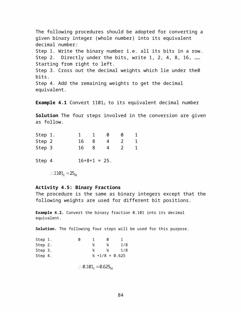
Figure 5.1: The three parts through which information is processed
Before, discussing the three parts through which information is processed, let us first look at the types of transducers.
Types of transducers
The types of transducers are given as follows: 1. Electromagnetic:
-Antenna- converts electromagnetic waves into electric current and vice versa. -Cathode ray tube (CRT) - converts electrical signals into visual form. -Flourescent lamp, light bulb - converts electrical power into visible light. -Magnetic cartridge - converts motion into electrical form. -Light-dependent resistor (LDR) - converts changes in light levels into resistance changes. -Tape head - converts changing magnetic fields into electrical form. -Hall effect sensor - converts a magnetic field level into electrical form.
2. Electrochemical: -pH probe. -Electro-galvanic fuel cell.
3. Electromechanical: -Rotary motor, linear motor. -Potentiometer when used for measuring position. -Load cell converts force to mV/V electrical signal using strain gauges. -Strain gauge. -Switch.
4. Electroacoustic: -Geophone - converts ground movement (displacement) into voltage. -Hydrophone - converts changes in water pressure into an electrical form. -Loudspeaker, earphone - converts changes in electrical signals into acoustic form. -Microphone - converts changes in air pressure into an electrical signal. -Piezoelectric crystal - converts pressure changes into electrical form. -Laser diode, light-emitting diode - convert electrical power into forms of light. -Photodiode. Photoresistor, phototransistor, photomultiplier tube - converts changing light levels into electrical form.
5. Electrostatic:
84
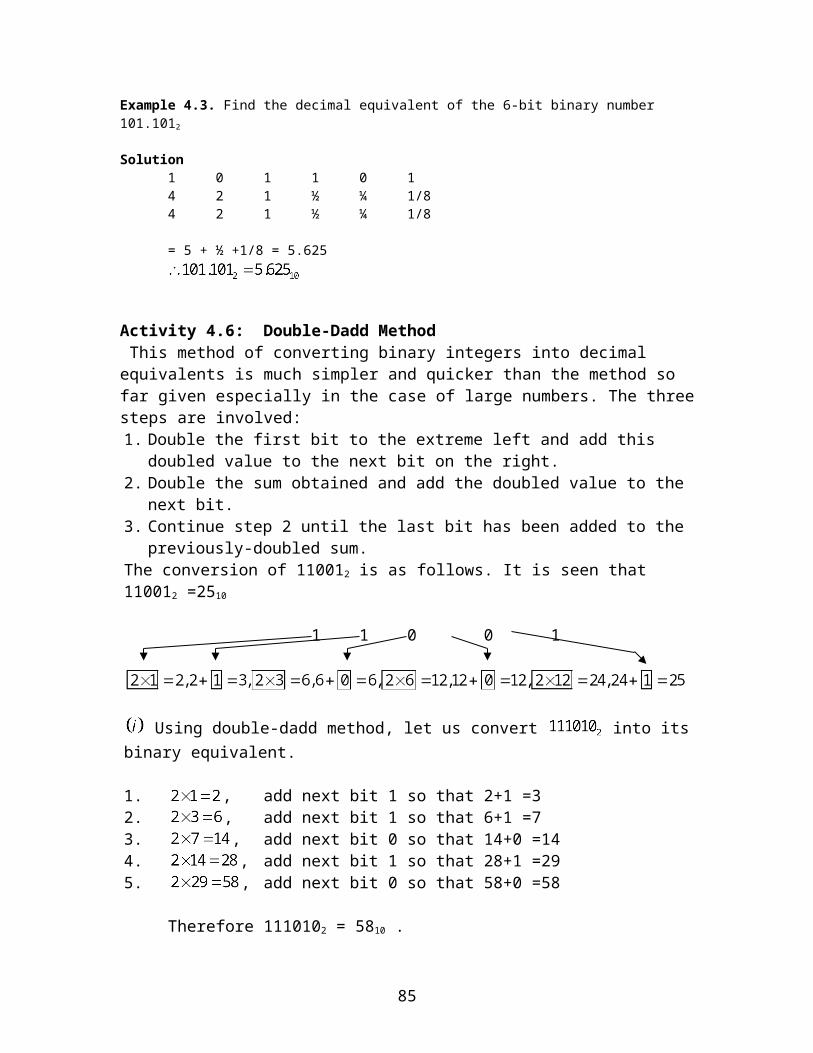
-Electrometer. -Liquid crysral dsiplay (LCD).
6. Thermoelectric: -RTD Resistance Temperature Detector. -Thermocouple. -Thermistor (includes PTC resistor and NTC resistor).
Task 5.1: Further Reading and Note making
You are required to use the references, "http://en.wikipedia.org/wiki/Transducer"; 8th October 2007.; http://soundlabs.princeton.edu/learning tutorials/sensors/node7, 12th August 2007., to make brief notes. You need to use the links within the reference in order to enrich the notes. Explain the operation of a transducer in the following modes
Strain Light, Piezo and Temperature
Activity 5.1.3: Brief Notes on sensor, signal conditioning and Data acquisition
In this section, the three stages of processing information in Fig. 5.1 are briefly discussed as follows. Most of the concepts are provided, thus what you need to do is to concentrate on understanding the concepts provided hereunder.
The Sensor Sensors can be categorized by the underlying physics of their operation, although one physical principle can be used to explain many different phenomena. For example, the piezoelectric effect can measure force, flexure, acceleration, heat, and acoustic vibrations. However, one phenomenon can also be measured by many physical principles. For example, sound waves can be explained by the piezoelectric effect, capacitance, electromagnetic field effects, and changes in resistance.
Signal Conditioning
The information from a sensor must be changed to a form appropriate for input into the data acquisition system. This means changing the sensors output to a voltage (if it isn't already), modifying the sensors dynamic range to maximize the accuracy of the data acquisition system, removing unwanted signals, and limiting the sensor's spectrum. In some cases, analog signal processing (both linear and
85
nonlinear) are desired to alleviate processing load from the data acquisition system and the computer.
Data Acquisition
The analog and continuous time signals measured by the sensor and modified by the signal conditioning circuitry must be converted into the form a computer can understand. This is what is referred to here as data acquisition.
Activity 5.1.4: Sensors
In this activity you will explain the operation of some of the sensors:
1. Pizoelectric sensors; and force sensing resistor; and microphones.2. The notes provided must be supplemented at all times.
Piezoelectric Sensors
The Piezoelectric effect is an effect in which energy is converted between mechanical and electrical forms. When a pressure is applied to a piezoelectric, the resulting mechanical deformation results in an electrical charge. For example, Piezoelectric microphones turns acoustical pressure into a voltage. Alternatively, when an electrical charge is applied to a polarized crystal, the crystal undergoes a mechanical deformation which can in turn create an acoustical pressure. (Read more about this).
How a voltage is created in a polarized crystal
Figure 5.2: Internal Structure of an electret
Solids which have permanent electrical polarization are called electrets, Fig. 5.2. Similar permanent polarization is also observed in crystals where, each cell of the crystal has an electric dipole, oriented such that the electric dipoles are aligned. But, this results in excess surface charge which attracts free charges from the surrounding atmosphere which makes the crystal electrically neutral. If a sufficient force is applied to piezoelectric crystal, the deformation which takes place disrupts the orientation of the electrical dipoles and a situation where
86
charge is not completely canceled is created. This results in a temporary excess of surface charge, which subsequently manifests as a voltage that is developed across the crystal.
Figure 5.3: A sensor based on the piezoelectric effect
If the surface the charge on a crystal is known, this physical principle is used to make a sensor which measures force. A force sensor is made of a capacitor formed by sandwiching a piezoelectric crystal between two metal plates as shown in Fig. 5.3. When an external force acts on a crystal, a charge, which is a function of the applied force is created due to defomation of the crystal. This charge results into a voltage, V given by Eq. 5.1
is the charge resulting from a force f, and C is the capacitance of the device.
As described above, piezoelectric crystals act as transducers which turn force, or mechanical stress into electrical charge which in turn can be converted into a voltage. Conversely, if one applies a voltage to the plates of the system in Fig. 5.3, the resultant electric field causes the internal electric dipoles to re-align which would cause a deformation of the material. An example of this is that piezoelectric transducers find use both as speakers (voltage to mechanical) and microphones (mechanical to electrical).
Task 5.2: Further reading and Note making
Use Compulsory Reading 5, and other references to write notes explaining the principles and operation of
Force sensing resistors.
Accelerometer (Analog Devices ADXL50).
Microphones.
Activity 5.1.5: Signal Conditioning
Requirements for A-D converters
87
The primary purpose for the analog signal conditioning circuitry is to modify the sensor output into a form that can be optimally converted to a discrete time digital data stream by the data acquisition system. Some important input requirements of most data acquisition systems are:
1. The input signal must be a voltage waveform. The process of converting the sensor output to a voltage can also be used to reduce unwanted signals, i.e., noise.
2. The dynamic range of the input signal should be at or near the dynamic range of the data acquisition system (usually equal to the voltage reference level, , or 2* ). This is important in maximizing the resolution of the analog to digital converter (ADC).
3. The source impedance, , of the input signal should be low enough so that changes in the input impedance, , of the data acquisition system do not affect the input signal.
4. The bandwidth of the input signal must be limited to less than half of the sampling rate of the analog to digital conversion.
Short Notes on Additional Requirements for Signal Conditioning
There are many other uses for the signal conditioning circuitry depending on a particular application. Some of these are:
(i) Signal isolation In many applications it is necessary to isolate the sensor from the power supply of the computer. This is done in one of two ways: magnetic isolation or optical isolation.
(ii) Signal preprocessing Generally it is desirable to perform preprocessing on the sensor signal before data acquisition in order to lower the required computer processing time, lower the necessary system sampling rate, or even perform functions that will enable the use of a much simpler data acquisition system entirely.
(iii) Removal of undesired signals Many sensors output signals may have many different components. Some of these additional signals may corrupt the sensor output need to to be removed before the signal is digitized. The ``noise'' which results from the undesired signals can also be removed using analog circuitry. For example, 60Hz interference can distort the output of low output sensors. The signal conditioning circuitry can remove this before it is amplified and digitized.
88
Voltage to Voltage
Motivation
Many sensors output a voltage waveform. Thus no signal conditioning circuitry is needed to perform the conversion to a voltage. However, dynamic range modification, impedance transformation, and bandwidth reduction may all be necessary in the signal conditioning system depending on the amplitude and bandwidth of the signal and the impedance of the sensor.
As you proceed from this stage, it is important to review the analysis of ideal op-amp circuits discussed in activity 3 (Non-Inverting ,The Summing Amplifier…).
Circuits: Amplifiers
Inverting The most common circuit used for signal conditioning is the inverting amplifier
circuit shown in Fig. 5.4. The voltage gain of this amplifier is . Thus the level
of sensor outputs can be matched to the level necessary for the data acquisition system. The input impedance is approximately and the output impedance is nearly zero. Thus, this circuit provides impedance transformation between the sensor and the data acquisition system.
Figure 5.4: Inverting Amplifier
The voltage swing of the output of the amplifier is limited by the amplifier's power supply as shown in Fig. 5.5. In this example, the power supply is +/- 13V. When the amplifier output exceeds this level, the output is ``clipped''.
89
Figure 5.5: Clipping of an Amplifier's OutputThe bandwidth is limited in the same way as dynamic range of the amplifier. The gain-bandwidth of an Op-amps is fixed. When an op-amp gain-bandwidth is connected to have a gain of 100, then the bandwidth of the amplifier will be limited to . All op-amps introduce noise to the signal and this is a major limitation of the amplifier circuit. Resistors also introduce noise in the circuit. The equation for this thermal noise is
where k is Boltzmann's constant, T is the temperature, B is the bandwidth of the measurement device, and R is the value of the resistance.
Anothere limitation of the op-amp is offset voltage. All op-amps have a small amount of voltage present between the inverting and non-inverting terminals. This DC potential is then amplified just as if it was part of the signal from the sensor.
Instrumentation amplifier
Possibly the most important circuit configuration for amplifying sensor output is the instrumentation amplifier (IA). An IA should have:
1. Finite, accurate and stable gain, usually between 1 and 1000. 2. Extremely high input impedance. 3. Extremely low output impedance 4. Extremely high CMRR.
Note that CMRR (common mode rejection ratio) is defined as:
90
Where:
differential-mode gain
common-mode gain
The difference amplifier described here, does not satisfy the second requirement of high input impedance. This problem is solved by placing a non-inverting amplifier at each one of the inputs to the difference amplifier as shown in Fig. 5.6. Remember that a non-inverting amplifier has a nearly infinite input impedance. In Fig. 5.6, the two resistors are connected together to create one common resistor,
instead of grounding the resistors. The overall differential gain of the circuit is given by Eq. 5.6:
Figure 5.6: Instrumentation AmplifierExample: Numerical Calculation
Determine the overall gain of the amplifier in Fig. 5.6 if
Solution
Lowpass and highpass active filters
The bandwidth of the incoming signal can be limited by modifying the non-inverting amplifier as shown in Fig. 5.7. That is, the feedback resistor is replaced with a resistor/capacitor combination. Thus the gain of the circuit is now given by Eq. 5.7.
91
where: and
Figure 5.7: Single Pole Low-Pass Filter
Activity 5.2: Current to Voltage
In this section you will learn how current output of a sensor can be converted into a voltage.
Activity 5.2.1: Motivation
Some sensors output a current rather than a voltage. The most common sensor of this type is the photodiode which has a current output proportional to the amount of light shining on it. In this case, the signal conditioning circuitry is required to convert the current output of the sensor to a voltage.
Activity 5.2.2: Circuits
An inverting amplifier configuration is used instead of a non-inverting amplifier in converting a current to a voltage. This is because a non-inverting amplifier draws very little current. Fig. 5.8 shows a current amplifier connected to a photodiode.As the light increases, the current output of the photodiode increases, thus increasing proportionally:
Figure 5.8: Photocell Connected to a Current Amplifier
92
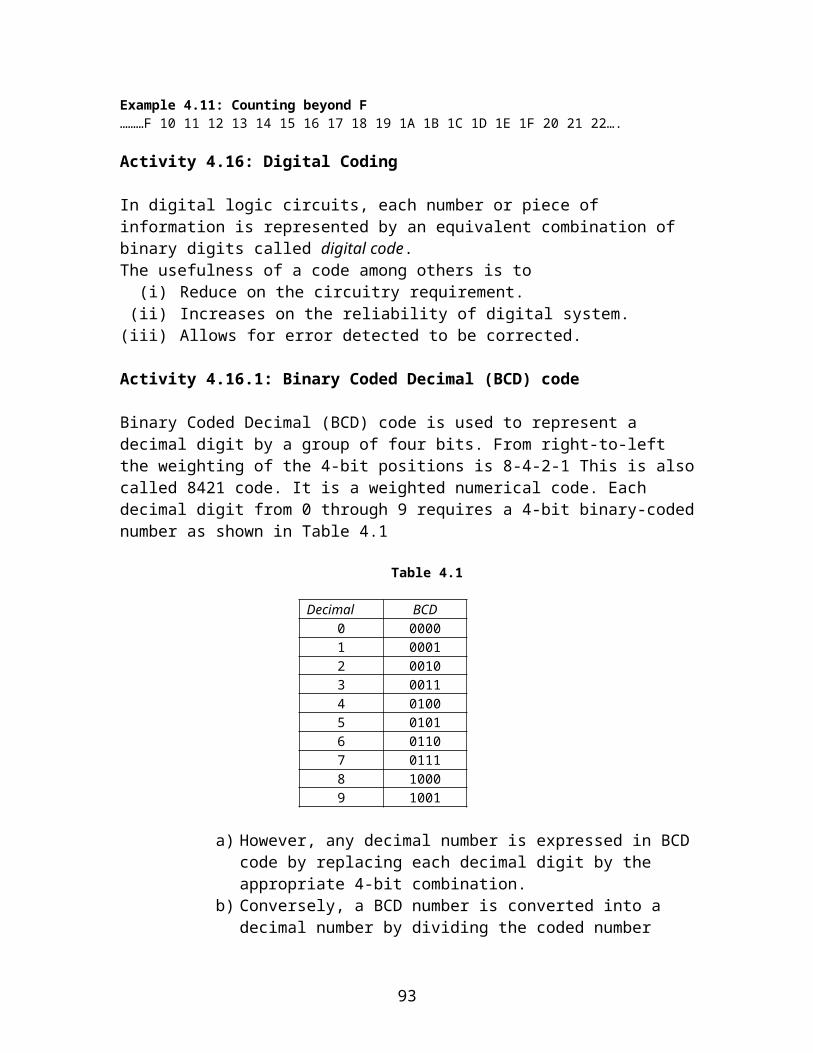
Activity 5.3: Resistance to Voltage
Activity: 5.3.1 Motivation
Many sensors cause changes in electrical resistance in response to the quantity they measure. For example in force sensing resistors, their resistances decrease when a force is applied, in thermistors the resistance change as a function of the temperature and in carbon microphones their resistance alter in response to changing acoustical pressure. What is therefore needed here is to convert the resistance of the device into a usable voltage which can be read by the analog to digital converters. Some circuits which perform these measurements are described as follows.
Activity 5.3.2: Circuits
There are two ways to convert resistance of a sensor to a voltage. The first, and simplest way is to apply a voltage to a resistor divider network composed of a reference resistor, , and the sensor, , as shown in Fig. 5.9.
Figure 5.9: Resistance to Voltage
The voltage that appears across the sensor (or the reference resistor) is then buffered before being sent to the ADC. The output voltage is given by Eq. 5.10
In this case, the amplifier amplifies the entire voltage measured across the sensor, and yet it is much better to amplify only the change in the voltage due to a change in the resistance of the sensor. This is achieved by using a bridge as shown in Fig. 5.10.
93
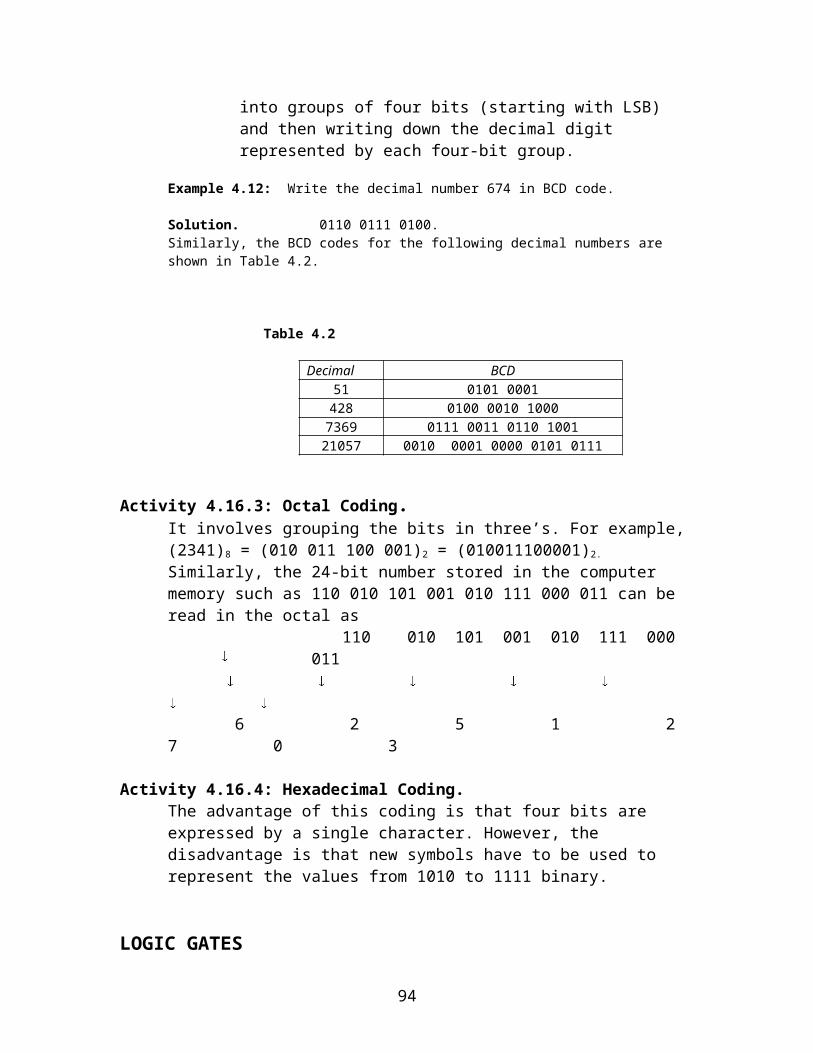
Figure 5.10: A Resistance Bridge Connected to an Instrumentation Amplifier (IA)
If is set equal to R, then the approximate output of this circuit is given by Eq. 5.11.
Where A is the gain of the IA and is the change in the resistance of the sensor corresponding to some physical action. Here only, is being amplified.
Activity 5.4: Capacitance to Voltage
Activity 5.4.1: Motivation
The electrical property of capacitance is a physical principle behind many of the sensors because it is a property which varies directly proportionally to the distance between the metal plates.
Capacitors can be used as sensors which can detect the presence of an object between their plates. This is because capacitors are sensitive to the material that resides between their metal plates. Thus, this principle can be used as a detector to determine when someone enters a space. In the case of the piezoelectric sensor, we use the fact that the voltage of a charged capacitor will vary inversely proportional to its capacitance. The output voltage is amplified to a usable level by an op-amp circuit.
Activity 5.4.2: Circuits
This activity briefly describes how capacitance can be measured. It should be noted that capacitance can be measured in the same ways for measuring resistance i.e by using a voltage divider or a bridge circuit, See Fig. 5. 9 and Fig. 5.10. Instead of using resistors, capacitors are used. However, one critical difference is that must be a sinusoidal signal since the capacitor blocks DC.
Activity 5.5: Data Acquisition
94
In this section you will learn about the functions of the different sections of data acquistion. Fig. 5.11 shows the steps into which Data acquisition can be divided. Each step of the data acquistion process: Anti-aliasing; sample/Hold ; and Quantization are described as follows.
.
Figure 5.11: Data Acquisition .
Activity 5.5.1: Anti-aliasing
The essential requirement is that all signals must be bandlimited to less than half the sampling rate of the sampling system. For broad spectrum signals, an analog lowpass filter must be placed before the data acquisition system. The minimum attenuation of this filter at the aliasing frequency should be at least:
Where B is the number of bits of the ADC. This formula is derived from the fact that there is a minimum noise level inherent in the sampling process and there is no need to attenuate the sensor signal more than to below this noise level.
Task 5.3: Further reading and Note making
Use Compulsory Reading 5 and other references to write short notes on-the problems with the Anti-aliasing Filter:-how the problems can be solved.
Activity 5.5.2: Sample and Hold
In this section you will learn that:
The purpose of the sample and hold circuitry is to take a snapshot of the sensor signal and hold the value. This happens once every sample period when the switch connects the capacitor to the signal conditioning circuit. During this period, the capacitor holds the voltage value measured until a new sample is acquired. Amidst all these the ADC must have a stable signal in order to accurately perform a conversion. Fig. 5.13 is an equivalent circuit for the sample and hold circuit. Many times, the sample and hold circuitry is incorporated into the same integrated circuit package.
95
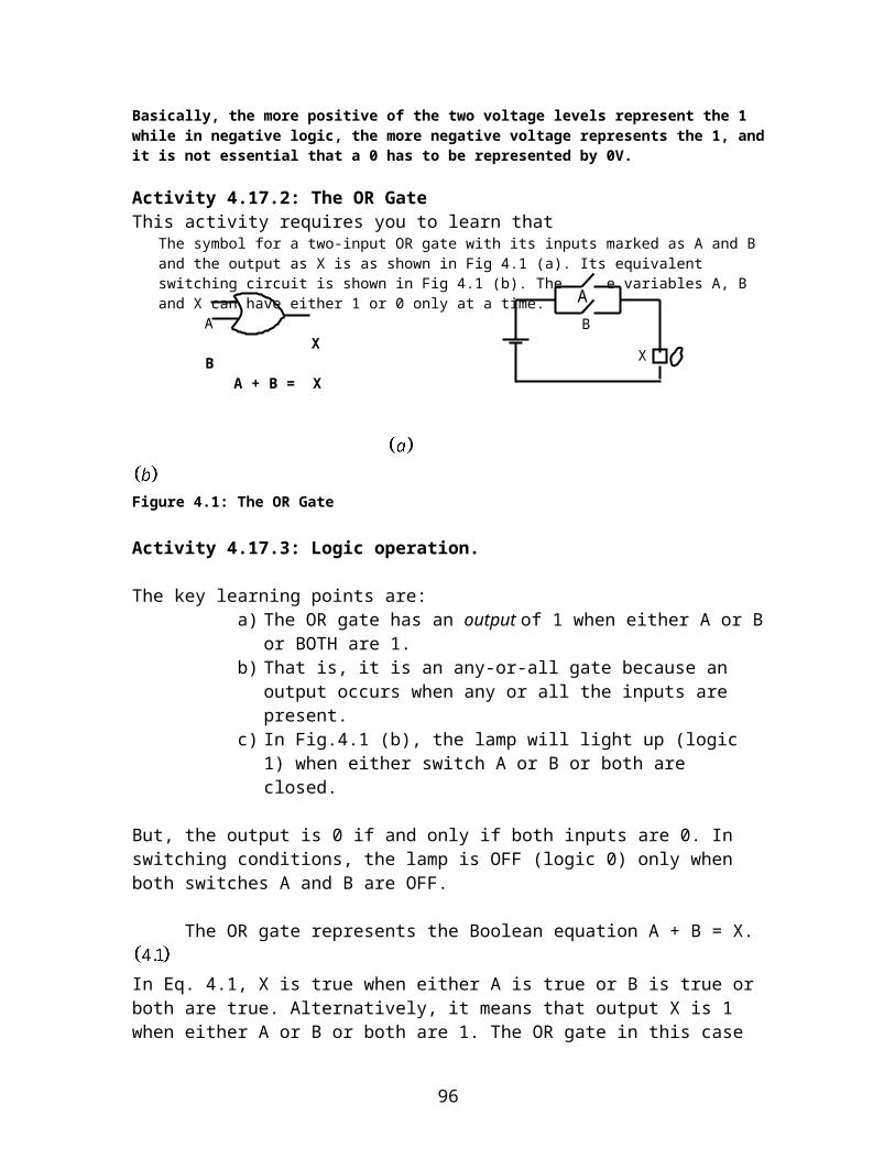
C
Figure 5.13: Equivalent Circuit for a Sample and Hold
However, a Sample and Hold circuit has problems which are attributed to: Finite Aperture Time; Signal Feedthrough; and Signal Droop.
Activity 5.5: Analog to Digital Conversion
In this section you will learn that:
(i) The purpose of the analog to digital is to quantize the input signal from the sample and hold circuit to 2B discrete levels - where B is the number of bits of the analog to digital converter (ADC).
(ii) The input voltage can range from 0 to (or to + for a bipolar ADC). What this means is that the voltage reference of the ADC is used to set the range of conversion of the ADC.
(iii) For a monopolar ADC, a 0 V input will cause the converter to output all zeros.
(iv) If the input to the ADC is equal to or larger than then the converter will output all ones.
(v) For inputs between these two voltage levels, the ADC will output binary numbers corresponding to the signal level.
(vi) For a bipolar ADC, the minimum input is and not 0 V.
1. Problems with ADC
ADC have problems due to noise in the quantized output signal. This is because it outputs only levels. The ratio of the signal to this quantization noise is called SQNR. The SQNR in decibels (dB) is approximately equal to 6 times the number of bits of the ADC given by Eq. 5.13.
For a 8 bit ADC, the SQNR is approximately equal to 48dB. However, other sources of noise that corrupts the output of the ADC include noise from the sensor, from the signal conditioning circuitry, and from the surrounding digital circuitry.
2. How to reduce the noise
96
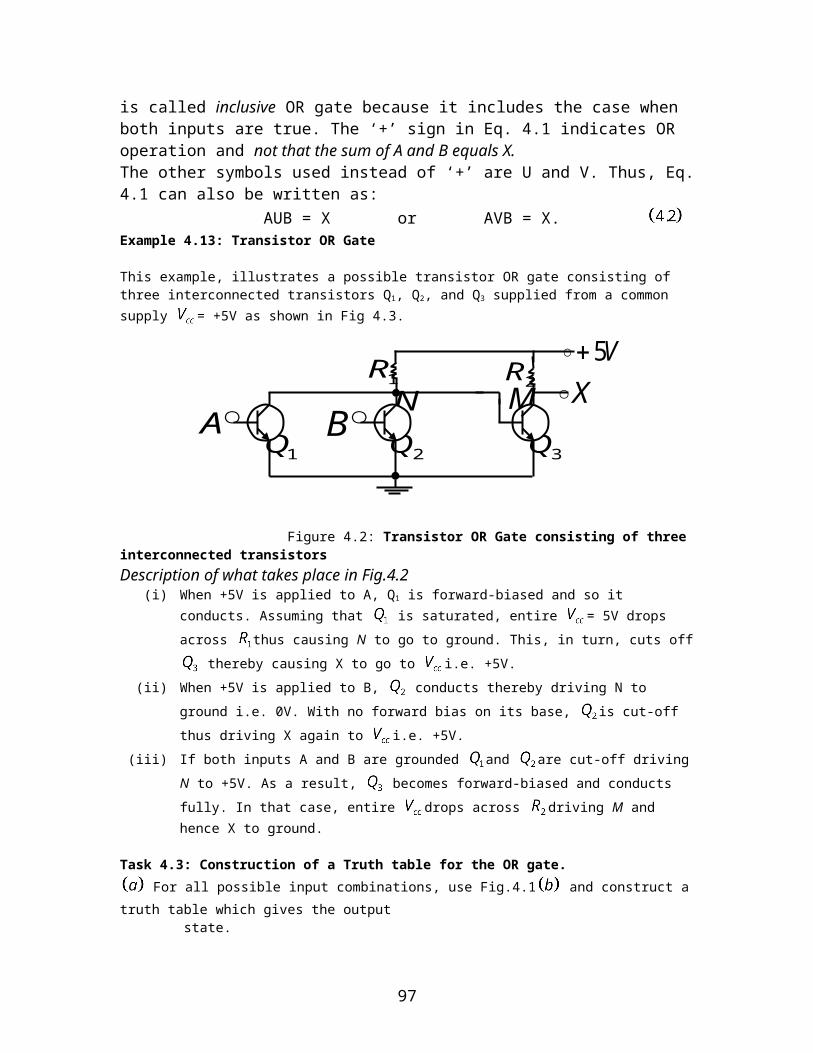
The effects of the noise can be reduced by maximizing the input signal level. That is by increasing the gain of the signal conditioning circuitry until the maximum sensor output is equal to the of the ADC. It is also possible to reduce the down to the maximum level of the sensor. The problem with this is that the noise will corrupt the small signals. A good rule of thumb is to keep at least as large as the maximum digital conversion signal, usually 5V.
Activity 5.6: System Integration
Figure 5.14: Block diagram of the National Instruments data acquisition card
Activity 5.6.1: Data Acquisition system
Fig. 5.14 depicts a simplified hardware block diagram of the National Instruments data acquisition card that can be used in the lab portion of a class. It has 16 analog channels which can either be configured as 16 single ended inputs, or 8 differential inputs. This is accomplished by the multiplexer, or switching circuit and is software configurable.
The output of the multiplexer feeds into an amplifier whose gain is programmable through software. This circuit allows the programmer to select an amplification appropriate to the signal that is to be measured. The board used in the lab is capable of implementing gains from 0.5 up to 100. As an example of how this programmable gain would be used, consider a bipolar (both positive and negative) input signal. The analog to digital converter has an input voltage range of V, hence a gain of 0.5 would enable the board to handle voltages ranging between V (5/0.5). Similarly, a gain of 100 would result in a maximum range of mV (5/100) at the input to the board.
97
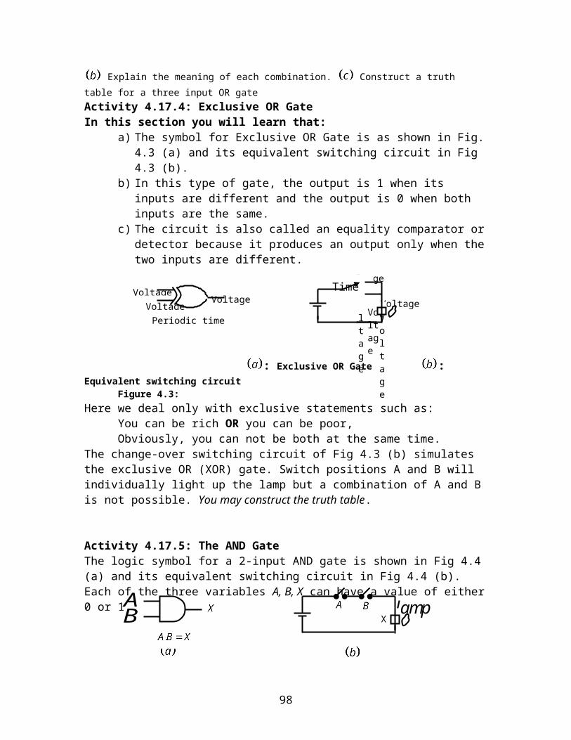
In addition to the analog to digital converters, there are 2 digital to analog converters which allow one to generate analog signals. Eight general purpose digital I/O lines are also provided which allow the board to control external digital circuitry or monitor the state of external devices such as switches or buttons.
Self evaluation 5.
1. (a) What is meant by the following? Finite Aperture Time.
Signal Feedthrough.
Signal Droop.
Describe how the problems in can be solved.
2. Explain what is meant by magnetic isolation and optical isolation.3. Explain the basic theory optical isolation.
ACTIVITY 6: Computers and Device Interconnection
You will require 15 hours to complete this activity. Only basic guidelinesare provided to help you go through the activity.
98
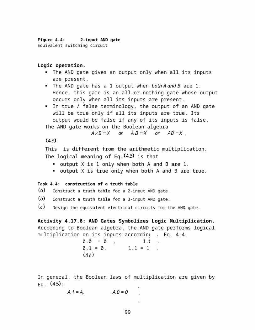
Specific Teaching and Learning Objectives
In this activity you will be expected to: Explain the systems level components of a microprocessor.
Summary of learning activityThe activity starts by first giving the definitions of the essential terms. This is followed by considerations of types and classification of computers such as analogue computers, digital computers and hybrid computers. In each case three main units of a computer:-Input devices, Output devices, and Central processing unit is discussed. In the case of CPU, a meaning of a term like 16 bit 64 K memory are clearly explained.
List of Reading Materials
Reading 7: Computers WIKIBOOKS
Reference: http://en.wikipedia.org/wiki/Computer. 4th October 2007.Abstract: The reference provides reading on stored programs architecture, and
how computer works. This includes control unit, arithmetic/logic unit (ALU), memory, input/output (I/O), multitasking, multiprocessing, and networking and internet.
Rationale: This provides a simple basic reading for someone beginning to learn about computer.
List of relevant MULTIMEDIA resources.
Reference: http://www.eastaughs.fsnet.co.uk/cpu/index.htm. 7th October 2007.Summary: Topics covered include computer tutorial, microprocessor tutorial that discusses about CPP structure and instruction to execution.Rationale:. This provides concise illustration and explanation of a computer.
List of Relevant Useful Links.
Title: ComputersURL: http://en.wikipedia.org/wiki/Computer 4th October 2007.Abstract: The resource provides reading on stored programs in architecture, and how computer works. This includes control unit, arithmetic/logic unit (ALU), memory, input/output (I/O), multitasking, multiprocessing, and networking and internet.
Title: Microprocessor. URL: http ://en.wikipedia.org/wiki/Microprocessor . 5th October 2007.Abstract: This providess some basic reading materials on: notable 8-bit designs, 16-bit
designs, 32-bit designs, and 64-bit designs in personal computers.
99
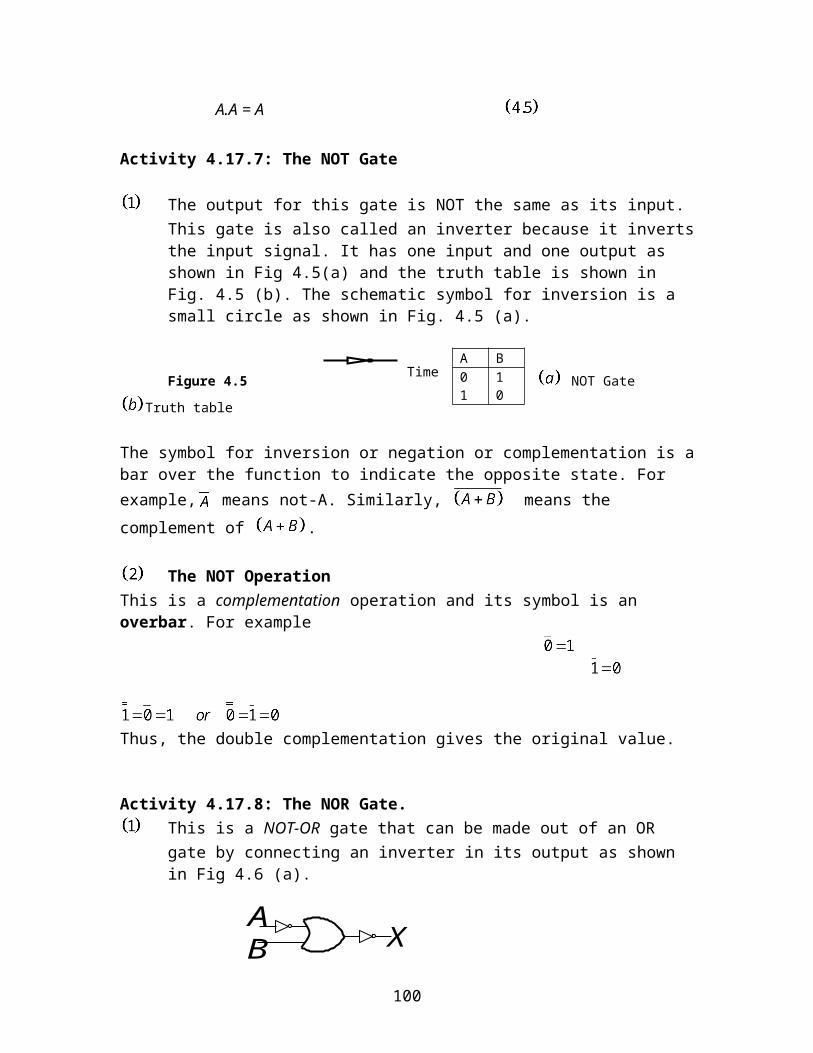
Title: 32-bit in computer architectureURL: http://en.wikipedia.org/wiki/32-bitAbstract: This gives the meaning of a 32-bit processor
Title: 8-bit in computer architecturehttp://en.wikipedia.org/wiki/8-bitAbstract. The topic includes list of 8 bits CPUs
Activity 6.1 Computer
In this activity we start by giving a definition of a digital computer before moving on to explaining the systems level components of a microprocessor
Activity 6.1.1:DefinitionA digital computer is a complex array of logic gates, registers, and associated circuitry organized to perform logic computation by manipulating waveforms representing digital numbers and words.
The circuits of digital computers are designed to carry out logic computations of all kinds. Therefore, the machine is furnished detailed instructions pertaining to every specific step in the calculation desired, as well as all of the digital numbers involved. The complete set of instructions is called the program and is stored within the computer. Since the program and data are easily changed for different problems, the stored-program digital computer is a very flexible and powerful processing instrument.
Activity 6.1.2: Types of computers
In this activity you will learn that computers may be divided according to size and memory. These include:a. Micro computers. A micro or personal computer is the smallest general
purpose computer system. It can execute programme to perform a variety of instructions. Such computers usually have a 8, 16 or a 32 bit microprocessor. An 8-bit microprocessor means that it can process 8 bits or 1 byte of data at a single given time.
b. Minicomputers. A minicomputer system is a small general purpose computer. The minicomputers are multi-user computers in contrast to the micros. They are very useful in distributed data processing networks. Most of the minicomputers designed now-a-days are with the 32-bit microprocessor.
c. Mainframe computers. A mainframe computer system is a fast computer, can process data much faster, and as several microprocessors are used in place of the single one used in micro and minicomputer systems. 2 to 8 bytes can be operated automatically in the same unit of time.
d. Super computers. Super computers are the most powerful and expensive computers. The time required to execute a single operation may even be of
100
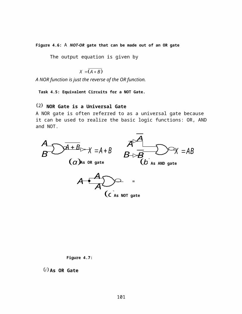
CPU
Arithmetic & Logic Unit
Main memory
Control Unit
OutputInput
the order of nanoseconds. Such computers are very much useful in research and defence.
Activity 6.1.3: Classification of computers
In this section you will learn that computers may also be classified according to the data they process. The classification include analogue computers, digital computers and hybrid computers
a) Analog computers. (i) handle data that is represented by physical quantities of continuously
variable size such as voltage current, temperature, length etc. (ii) get up the mathematical analog of the problem.
However and an analogue computer is less accurate (1 part in ) and has limited memory.
b) Digital computers. These handle actual numbers expressed in digits and the qualities in the problem are represented by discrete numbers. The pulse circuitry is used in such computers. It breaks down the problem into logical arithmetical steps. It has very large memory and is highly accurate ( 1 part in 1012 or more)
c) Hybrid computers. The hybrid computers are those in which the desirable characteristics of both analog and digital computers are integrated.
Activity 6.1.4: Essential components of a computer system.
In this activity you learn about the functions of the main units of a computer. A computer can be divided into three main units:
-Input devices, Output devices, and Central processing unit.
The block diagram of a computer system is shown in Fig 6.1.
101
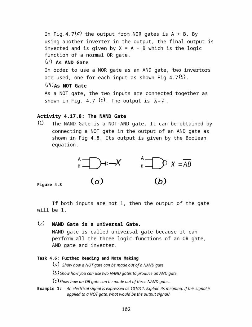
Figure 6.1: Block diagram of a Computer system
Input devices. The necessary data and instructions are fed to the computer through the input device of the computer. The input devices can basically be divided into two types:
-Direct input devices, and Indirect input devices
The direct input devices consists of: Key board, Data entry terminal, Bar code reader, Tourch screen (visual display unit), light pen, Input table, Mouse, Voice drive ,Magnetic ink character reader, and Optical character reader.
While the indirect devices consists of: Punched card reader, Floppy disk reader,compact disks, memory sticks and Magnetic tape Reader.
Output devices. These devices take the output generated from the computer in the machine code and either convert it into a form understandable by human beings or store in some convenient manner. The output devices may be divided into three categories: Displayed output, Printed output, and Stored output. Most of the computers have display devices. The display devices are cathode ray tube (CRT). The plasma display has come into the limelight in the portable computers. The printed output device generates the output in the printed form on paper. The printers may be broadly divided into following four types:
-Dot matrix printers, Letter quality printers, Line printers, Laser printers. The different forms of stored output also known as secondary storage of the system are as follows:
-Punched paper, Magnetic tape, Magnetic disk, RAM disc storage, Magnetic bubble storage, Optical disk.
Central Processing Unit (CPU). The CPU is the heart of the computer and consists of three components namely:
-Memory or main storage, Arithmetic and logic unit, and Control UnitAll these components are electronic circuits. The main storage or memory area may be divided into four sections as follows:
- Input storage area where data is held until it is processed
102
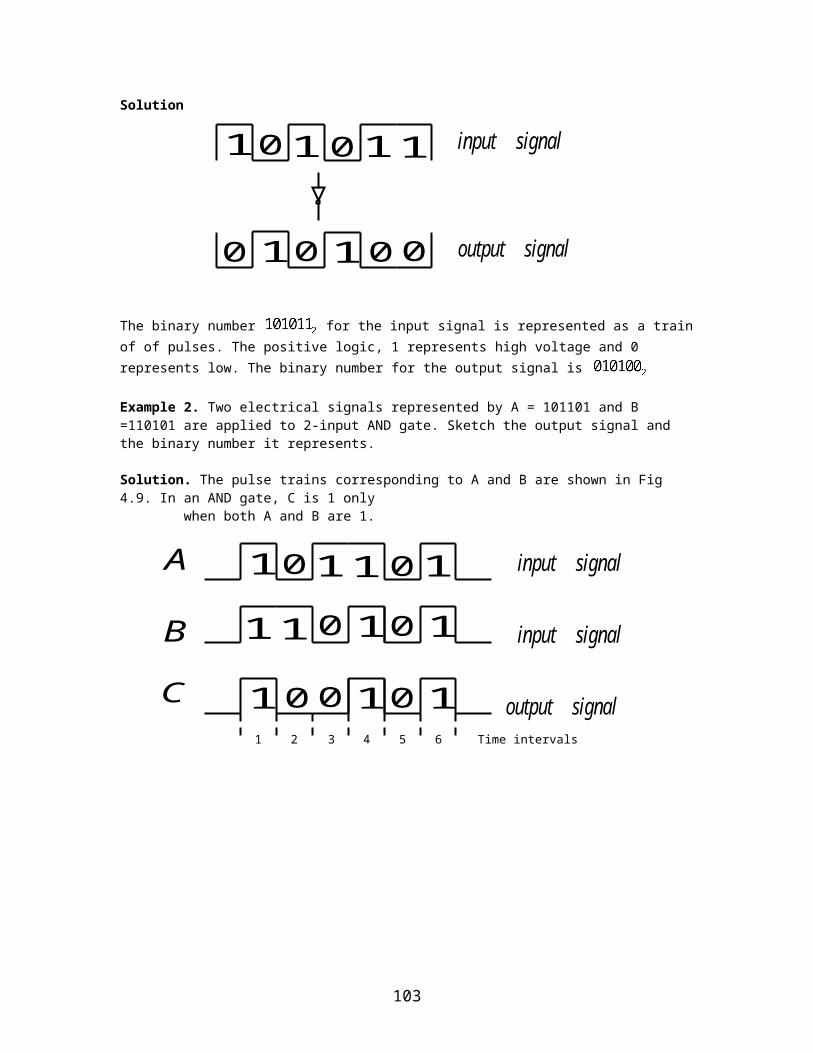
- Programme storage area where the processing instructions area held.- Working storage area (scratch pad) where intermediate data is held while being processed.- Output storage area where the final results are held.
The main storage memory is of two types:-magnetic core memory.-Semiconductor memory.
The former type is non volatile i.e., does not cease to store data when supply is switched off. It is now almost superceded by the latter type. The semiconductor memories are faster to access, more compact and cheap. The common types are:
- Random access Memory (RAM), - Read Only Memory (ROM), - Programmable ROM (PROM), - Erasable PROM (EPROM).
The memory is measured in terms of words, location or addresses.
For example number of bytes in a 16 bit 64 K memory is given as follows: 16 bit 64 K memory = 64 * 1024 locations
= 64 * 1024 * 16 = 1048576 bits = 131072 bytes,
Where 1 byte = 8 bits of storage locations and 1 K = 1024 locations.
Activity 6.2: Microprocessor
In this activity we learn about a microprocessor and then we explain its system level components.
A microprocessor is a computer processor on a microchip. It's sometimes called a logic chip. It is the "engine" that goes into motion when you turn your computer on. A microprocessor is designed to perform arithmetic and logic operations that make use of small number-holding areas called registers. Typical microprocessor operations include adding, subtracting, comparing two numbers, and fetching numbers from one area to another. These operations are the result of a set of instructions that are part of the microprocessor design. When the computer is turned on, the microprocessor is designed to get the first instruction from the basic input/output system (BIOS) that comes with the computer as part of its memory. After that, either the BIOS, or the operating system that BIOS loads into computer memory, or an application program is "driving" the microprocessor, giving it instructions to perform.
In short the microprocessor is the integration of a number of useful functions into a single IC package. These functions are:
103
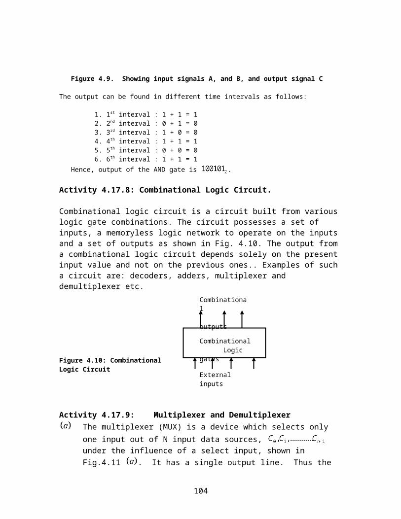
a. The ability to execute a stored set of instructions to carry out user defined tasks.
b. The ability to be able to access external memory chips to both read and write data from and to the memory.
Activity 6.2.1: Computer Architecture
You will learn that:a. The major parts of a digital computer can be interconnected in various ways to
emphasize different operating features.b. The internal structure of each part may be configured to perform certain tasks
most efficiently. These aspects of digital computer design are referred to as computer architecture.
Activity 6.2: Architecture of microprocessors
This activity deals with learning of architecture of microprocessors which include: memory organization, central processing unit, and input/output.
Activity 6.2.1: Memory Organization
Here you learn that the Read Only Memory (ROM), and Random Access Memory (RAM) used in microprocessor systems are based among others on Bipolar-transistor integrated-circuit gates (DTL NAND gate, TTL NAND gate, ECL NOR gate, I2L OR gate); and integrated-circuit MOSFET gates (NMOS NOR gate, CMOS NAND gate).
WRITE SHORT NOTES TO EXPLAIN THE FOLLOWINGa. Random access memory (RAM)b. Read only memory (ROM)
Learning Points Among other points you should learn that:
(i) One measure of the power of a microprocessor system is the memory capacity, for this determines the length of the program and the amount of the data that can be handled.
(ii) Ordinarily, the smallest unit of information accessed out of memory is one word, and that the most commonly used word length in microprocessor is an 8-bit word, called byte.
(iii) Memory words can be interpreted by the CPU in three fundamentally different ways: Pure binary numeric data; Instructions, and data code.
(iv) Binary data are the numerics associated with the program. For example, one memory byte can represent any number from 0000 0000, that is, 0 to 1111 1111, or 255.
Activity 6.2.2: Central Processing Unit (CPU)
104
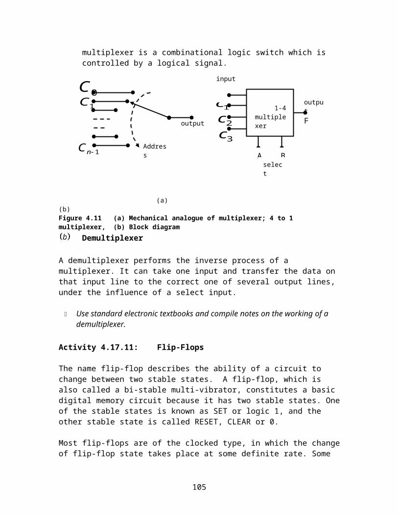
16-bit memory address
6-bit 10-bit chip select word select
In this activity you will learn that (i) Every CPU has at least one register in which data words fetched from memory
can be stored.(ii) The primary working register of the CPU is called accumulator.
(iii) The accumulator stores the data word to be operated upon by the CPU USE AVAILABLE REFERENCES AND WRITE SHORT NOTES TO EXPLAIN THE
WORKING OF THREE OTHER OPERATIONAL REGISTERS: instruction register; program register, and data counter.
Activity 6.2.3: Input/Output
This activity looks briefly at what happens in the input/output of the microprocessor. The key learning are that:
(i) In a complete microprocessor system, the CPU exchanges data and address words with memory chips and input/output or I/O devices.
(ii) A straight forward way to accomplish this is with a data bus and address bus, which are common signal paths interconnecting all devices. (The term bus is derived from the latin omnibus, which means “for all”).
(iii) The CPU may place an address word on the address bus which is decoded by each of the other chips and results in some appropriate response. This response, which might be for a memory chip to place the addressed memory word on the data bus, is triggered by an enabling signal on a control line, such as the read/write control line.
(iv) A commonly used address-word length in classic 8-bit microprocessors is composed of 16 bits, that is, 2 bytes.
(v) A popular convention is to assign the lowest 10 digits to the word address and the remaining 6 most significant binary digits to chip selection as shown below:
Using this convention , or 64, different memory chips (and/or I/O devices) can be selected and up to , or 1024, individual words on each chip can be addressed.
Most often I/O devices communicate with microprocessor through I/O interface buffer chips which are addressed by the CPU much like memory chips.
WRITE SHORT NOTES TO EXPLAIN WHAT IS MEANT BY THE FOLLOWING IN THE INPUT/OUTPUT
105
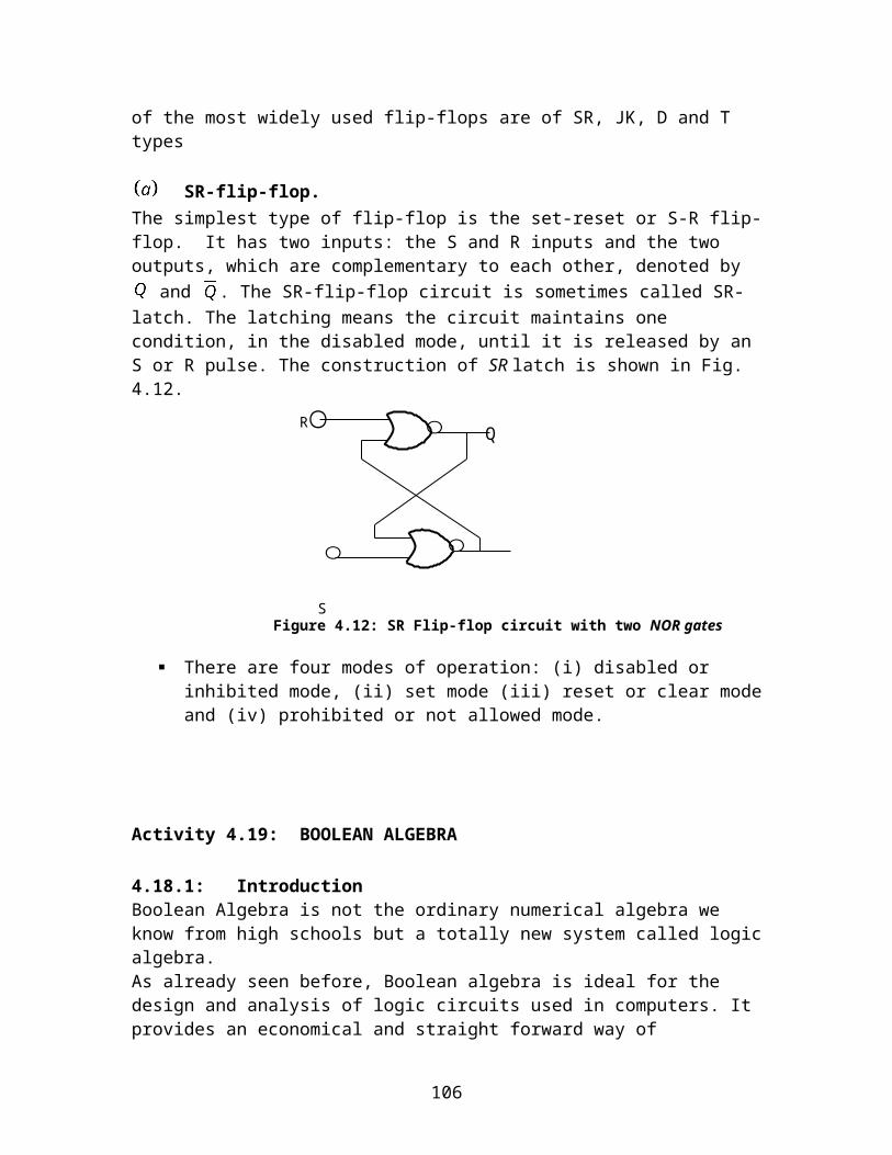
i. Interrupt prioritiesii. Direct memory access (DMA)
Activity 6.3: Encoder and Decoder.
In this activity we learn that in a computer:(i) The encoding process transforms the desired signals into binary words
which can be stored in memory for use when needed.(ii) The word length (number of bits) is much less than the number of lines.
(iii) The circuit of an encoder also has many input lines but the output is a coded pattern which identifies each of the inputs. For example seven input signals are encoded to produce three bit binary words.
In general a total of 2n – 1 input lines can be represented by n-bit binary words.
Example: Find the number of input lines that can be coded to
1. eight bit word2. sixteen bit word
SolutionTotal number input lines =
For 8-bit word, the total number of input lines = For 16-bit word, the total number of input lines =
Word lengths of 8, 16, 32 and 64 bits are in common use on computer systems. Words are often divided into eight-bit segments, called bytes.
Example: To determine the minimum number of bits required
A keyboard on which there are 26 lower case and 26 capital letters, 10 numericals and 22 special characters needs a total number of 84= codes if we require to transmit a binary code with every stroke of the key board
Since total number input lines = The number of bits, n, is determined as follows:
If n =6 then, . This is less than the required total of 84 codesIf n = 7 then, . This is greater than 84. Therefore a minimum of 7 bits will be required.
Activity 6.3.1: Illustration of an encoder A block diagram for such an encoder is shown in Fig 6.2. If the key is depressed, a switch, ,is closed then a 1V supply (corresponding to the 1 state) is connected to input line.
106
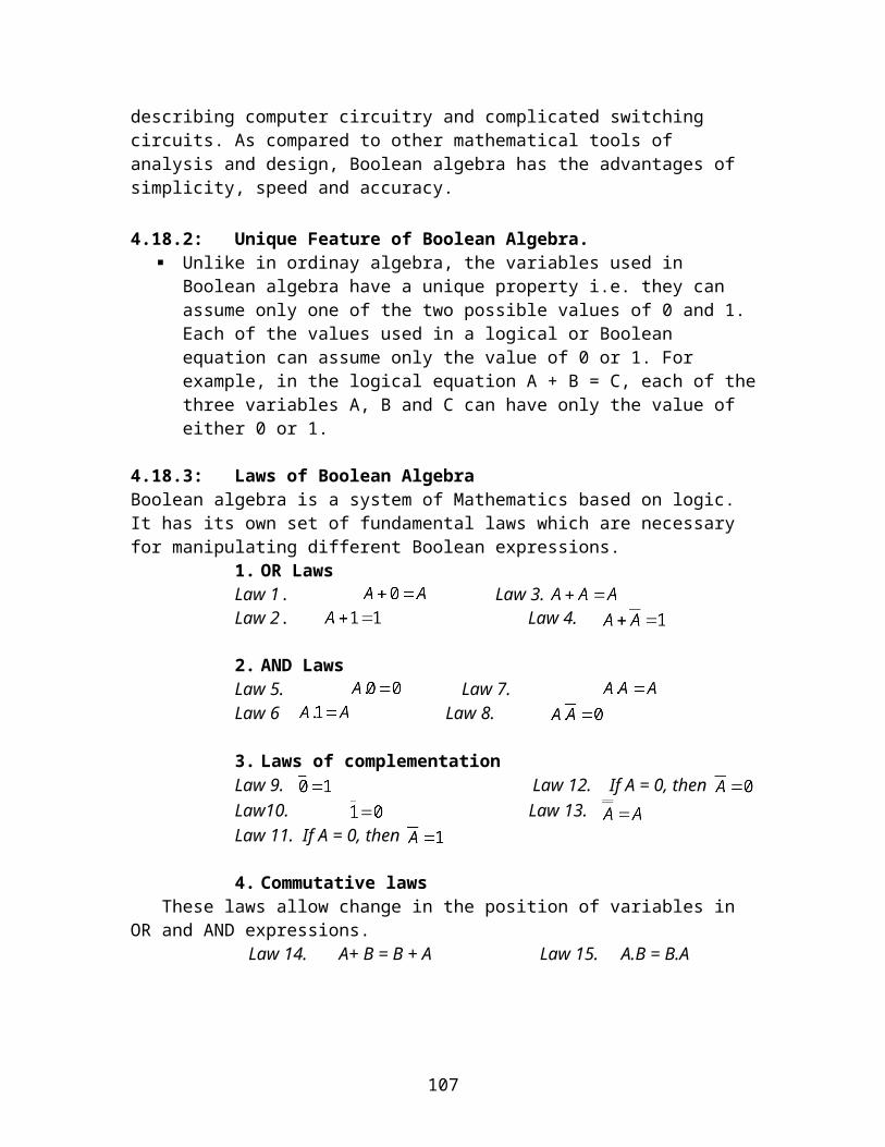
1V
0K
83K
A
B
C
D
E
F
G
1K
Encoder
Figure 6.2: Block diagram for keyboard encoder
Activity 6.4: Practical Microprocessors
In this activity the different practical microprocessors: 8-Bit systems, 16-Bit and 32-Bit CPUs are discussed and learnt.
Activity 6.4.1: 8-Bit Systems
In this activity you will learn that:(i) An 8-bit processors have instruction sets (78 instructions), chip architecture and
a 2- s instruction cycle.(ii) Both instruction and data words are 8-bits long.
(iii) But the address word length is 16 bits, which addresses , or 65,536 locations.(iv) Separate 8-bit data and 16-bit address buses communicate with peripheral chips,
and a region of RAM is reserved to act as the stack, which permits virtually unlimited subroutine nesting.
(v) Thus, in computer architecture, 8-bit integers, memory addresses, or other data units are those that are at most 8 bits (1 octet) wide. Also, 8-bit CPU and ALU architectures are those that are based on registers, address buses, or data buses of that size.
(vi) The first widely adopted 8-bit microprocessor was the Intel 8080, being used in many hobbyist computers of the late 1970s and early 1980s, often running the CP/M operating system.
WRITE A SHORT NOTE ON WHAT IS MEANT BY instruction cycle
Activity 6.4.1: 16-Bit Systems The key learning points here are that:
107
(i) Increased precision in microprocessor circuits is attained through the use of longer data words. For this, the 16-bit and 32-bit microprocessors are used.
(ii) It is desirable to use longer address words so that larger memories can be accessed and also faster clock speeds in order to reduce execution time.
(iii) Modern 16- and 32-bit chips achieve these goals by using longer lengths and also by employing advanced architecture.
(iv) A number of different parameters specify the performance of microprocessors and determine their suitability for any given application.
(v) Thus in computer architecture, 16-bit integers, memory addresses, or other data units are those that are at most 16 bit (2 octets) wide. Also, 16-bit CPU and ALU architecture are those that are based on registers, address buses, or data buses of that size.
(vi) The memory capacity is indicated by a commonly used power-of-2 convention. That is, K is the symbol for bytes, or kilobytes, andM signifies bytes, or one megabyte, whileG = bytes, or one gigabyte.
(vii) Prominent 16-bit processors include the PDP-11, INTEL 8086, Intel 80286 and the WDC 65C816. The Motorola 68000 was 16-bit in that its data buses were 16 bits long; however, it was 32-bit in that the general purpose registers were 32 bits long and most arithmetic instructions supported 32-bit arithmetic, and 24-bit in that the address bus was 24 bits long.
A 16-bit integer can store 216 (or 65536) unique values. In an unsigned representation, these values are the integers between 0 and 65535; using two’a component, possible values range from −32768 to 32767.
Activity 6.4.3: 32-Bit Systems The key learning points here are that:
(i) In computer architecture, 32-bit integers, memory addresses, or other data units are those that are at most 32 bits (4 octets) wide. Also, 32-bit CPU and ALU architecture are those that are based on registers, address buses, or data buses of that size. 32-bit is also a term given to a generation of computers in which 32-bit processors were the norm.
(ii) The range of integer values that can be stored in 32 bits is 0 through 4,294,967,295 or −2,147,483,648 through 2,147,483,647 using two’s complement encoding. Hence, a processor with 32-bit memory addresses can directly access 4 gigabytes of byte-addressable memory memory.
Activity 6.4.4: Kibibyte vs Kilobyte
In this activity we will differentiate between kibibyte and kilobyte. First, we define the kibibyte. That is,
108
A kibibyte (a contraction of kilo binary byte) is a unit of information or computer storage, established by the International Electrtechnical Commission in 2000. Its symbol is KiB.
1 kibibyte = 210 bytes = 1 024 byte You should note that:
The kibibyte is closely related to the kilobyte, which can be used either as a synonym for kibibyte or to refer to 10³ bytes = 1,000 bytes, whereby
1 kilobyte = = 1000 byteThus, the term kibibyte has evolved to refer exclusively to 1,024 bytes.
You should note that:If one expects power-of-two values to refer to capacity, and manufacturers use power-of-ten values, the difference could be substantial.
(i) With a kilobyte (1024 versus 1000), the difference is 2.4%. (ii) With megabyte (1024² or 1,048,576, versus 1,000,000 - a difference of 4.9%.
(iii) With "gigabytes", if one uses 1024³, the size of a drive would be expected to be 1,073,741,824 bytes per gigabyte versus a mere 1,000,000,000 - a difference of 7.4%.
This should tell you that, confusion can be compounded by the use of both 1,024 and 1,000 in a single definition.
The quoted capacity of 3½ inch HD floppy disks is 1.44 MB, where MB stands for 1000 times 1024 bytes. The total capacity is thus 1474560 bytes, or approximately 1.41 MiB.
ExampleThe above relation can be shown as follows:
1.44 MB = = 1474560 bytesDivide this by 1,048,576, i.e.
MiB
Thus, 1.44 MB floppy disks can store 1474560 bytes of data when MB means 1000 times 1024 bytes.
Self Evaluation 6
1. Explain the meaning of the term program in computing.2. Find the number of input lines that can be coded to 32 bit word3. Explain what is meant by an instruction and register in computing.4. Express 3.7MB in bytes MiB
SOLUTIONS TO SELF EVALUATION
109
Solution to Self Evaluation 11. (a) (b) 0.01859 s/m
2. This is because, by addition of donor impurity, the number of electrons available for conduction purposes becomes more than the number of holes available intrinsically. But the total charge of the semiconductor does not change because the donor impurity brings in as much negative charge (by way of electrons) as positive charge (by way of protons in its nucleus).
3. Barrier voltage depends on doping density, electronic charge and temperature. For a given junction, the first two factors are constant, thus making depending on temperature. With increase in temperature, more minority charge carriers are reduced, leading to their increased drift across the junction. As a result, equilibrium occurs at lower barrier potential. It is found that both for Ge and Si, decreases by about 2mV / ºC.
SOLUTION TO SEL EVALUATION 21. Physical features BJT are that
-The base is lightly doped, with high resistivity material. -The collector surrounds the emitter region, making it almost impossible for the electrons injected into the base region to escape being collected, thus making the resulting value of α very close to unity, and so, giving the transistor a large β. A cross section view of a BJT indicates that the collector–base junction has a much larger area than the emitter–base junction.-The bipolar junction transistor, unlike other transistors, is not a symmetrical device. This means that interchanging the collector and the emitter makes the transistor leave the forward active mode and start to operate in reverse mode. Because the transistor's internal structure is usually optimized to forward-mode operation, interchanging the collector and the emitter makes the values of α and β in reverse operation much smaller than those found in forward operation; often the α of the reverse mode is lower than 0.5. The lack of symmetry is primarily due to the doping ratios of the emitter and the collector. The emitter is heavily doped, while the collector is lightly doped, allowing a large reverse bias voltage to be applied before the collector–base junction breaks down. The collector–base junction is reverse biased in normal operation. -The reason the emitter is heavily doped is to increase the emitter injection efficiency: the ratio of carriers injected by the emitter to those injected by the base. -For high current gain, most of the carriers injected into the emitter–base junction must come from the emitter.
110
Small changes in the voltage applied across the base–emitter terminals causes the current that flows between the emitter and the collector to change significantly. This effect can be used to amplify the input voltage or current. BJTs can be thought of as voltage-controlled current sources, but are more simply characterized as current-controlled current sources, or current amplifiers, due to the low impedance at the base.NPN is one of the two types of bipolar transistors, in which the letters "N" and "P" refer to the majority charge carriers inside the different regions of the transistor. Most bipolar transistors used today are NPN, because electron mobilty is higher than hole mobility in semiconductors, allowing greater currents and faster operation.NPN transistors consist of a layer of P-doped semiconductor (the "base") between two N-doped layers. A small current entering the base in common-emitter mode is amplified in the collector output.The arrow in the NPN transistor symbol is on the emitter leg and points in the direction of the conventional current flow when the device is in forward active mode.A convenient mnemonic device for identifying the symbol for the NPN transistor and, by elimination, the PNP transistor is "NPN is Not Pointed iN."
Solution to Self Evaluation 3
1. A specific op-amp may be chosen for its: open loop gain, bandwidth, noise performance, input impedance, power consumption, or a compromise between any of these factors.2. 84.42 mV3 The output voltage is
Soultions to Self Evaluation 4
1. The following four steps will be used for this purpose. Step 1. 0 1 1 1Step 2. ½ ¼ 1/8Step 3. ½ ¼ 1/8Step 4. ½ + ¼ +1/8 = 0.875
4. 0.77 = 0.1100015. 25.625 = 11001.101
111
6. i- 13 and 26; ii- 13 and 6.5
This implies that shifting binary point to right is equivalent to multiplying the number by 2, while shifting the binary point to the left is equivalent to dividing the number by 2
5 a. 111b. 0010c. 0011
6. 11101000 1001111
7. i. X = AB + C ii. X = 1; and X = 1
8 The logic equation which provides the switching function is given by
For A = B = 0, we get F = ,
For A = 0, B = 1, we get F =
For A = 1, B = 0, we get F =
For A = 1, B = 1, we get F =
Thus for to be selected AB = 10, which enables and will appear at the output F
Solution to Self evaluation 5
1. -Finite Aperture Time: The sample and hold takes a period of time to capture a sample of the sensor signal. This is called the aperture time. Since the signal will vary during this time, the sampled signal can be slightly off.
-Signal Feedthrough: When the sample and hold is not connected to the signal, the value being held should remain constant. Unfortunately, some signal does bleed through the switch to the capacitor, causing the voltage being held to change slightly. -Signal Droop: The voltage being held on the capacitor starts to slowly decrease over time if the signal is not sampled often enough. The main solution to these problems is to have a small aperture time relative to the sampling period. This means that if the HCI designer uses a high sampling rate, the aperture time of the sample and hold must be quite small.
112
2 -Magnetic isolation is primarily used for coupling power from the computer or the
wall outlet to the sensor. This is done through the use of a transformer.
- Optical isolation is used for coupling the sensor signal to the data acquisition input. This is usually done through the use of a light emitting diode and a photodetector. This can be integrated into a single IC package such as the 6N139.
The Basic Theory Optical isolation has two basic elements: a light source(usually a light emitting diode) and a photo-sensitive detector. These twoelements are positioned facing one another and inserted in an electrical circuitto form an optocoupler. The key property of an optocoupler is that there is aninsulating gap between the light source and the detector. No current passesthrough this gap, only the desired light waves representing data. Thus the twosides of the circuit are effectively "isolated" from one another. PrimaryApplication In data communications, the primary application for optical isolation isin a point-to-point data circuit that covers a distance of several hundred feet ormore. Because the connected devices are presumably on different powercircuits, a ground potential difference likely exists between them. When such acondition exists, the voltage of "ground" can be different, sometimes by severalhundred volts.Where a ground potential difference exists, a phenomenon called groundlooping can occur. In this phenomenon, current will flow along the data line in aneffort to equalize the ground potential between the connected devices. Groundlooping can, at the very least, severely garble communications--if not damagehardware!Optical isolation solves the problem of ground looping by effectively lifting theconnection between the data line and "ground" at either end of the line. If anoptically coupled connection exists at each end, the data traffic "floats" abovethe volatility of ground potential differences.
Solution to self Assessment 6.
1. In computing, a program is a specific set of ordered operations for a computer to perform. In the modern computer, the program contains a one-at-a-time sequence of instructions that the computer follows. Typically, the program is put into a storage area accessible to the computer. The computer gets one instruction and performs it and then gets the next instruction. The storage area or memory can also contain the data that the instruction operates on. (Note that a program is also a special kind of "data" that tells how to operate on "application or user data.")
Programs can be characterized as interactive or batch in terms of what drives them and how continuously they run. An interactive program receives data from an interactive user (or possibly from another program that simulates an interactive user). A batch program runs and does its work, and then stops. Batch programs can be started by interactive users who request their interactive program to run the batch program. A command interpreter or a Web browser is an example of an interactive program. A program that computes and
113
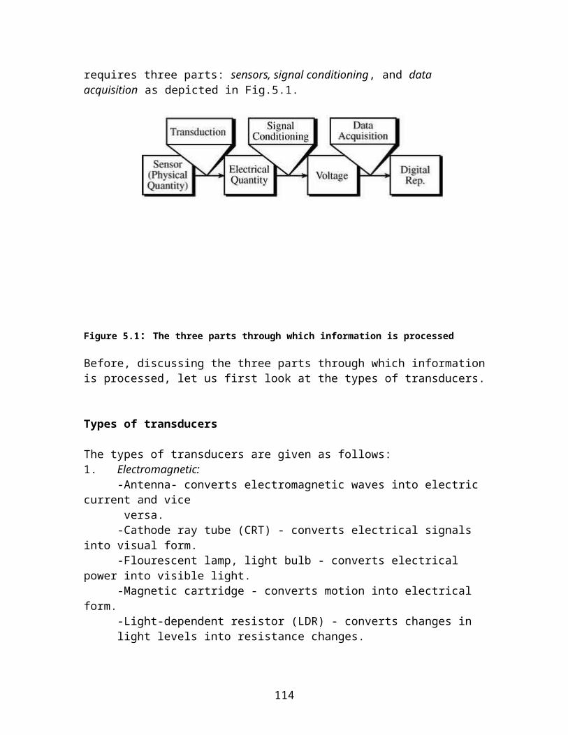
prints out a company payroll is an example of a batch program. Print jobs are also batch programs.
When you create a program, you write it using some kind of computer language. Your language statements are the source program. You then "compile" the source program (with a special program called a language compiler) and the result is called an object program. There are several synonyms for object program, including object module and compiled program. The object program contains the string of 0s and 1s called machine language that the logic processor works with.
The machine language of the computer is constructed by the language compiler with an understanding of the computer's logic architecture, including the set of possible computer instructions and the length (number of bits) in an instruction
2. For 32-bit word, the total number of input lines = 4294967295
3. InstructionAn instruction is an order given to a computer processor by a computer program. At the lowest level, each instruction is a sequence of 0s and 1s that describes a physical operation the computer is to perform (such as "Add") and, depending on the particular instruction type, the specification of special storage areas called registers that may contain data to be used in carrying out the instruction, or the location in computer memory of data. In a computer's assembler language, each language statement generally corresponds to a single processor instruction. In high-level languages, a language statement generally results (after program compilation) in multiple processor instructions
Register.In a computer, a register is one of a small set of data holding places that are part of a computer processor. A register may hold a computer instruction, a storage address, or any kind of data (such as a bit sequence or individual characters). Some instructions specify registers as part of the instruction. For example, an instruction may specify that the contents of two defined registers be added together and then placed in a specified register. A register must be large enough to hold an instruction - for example, in a 32-bit instruction computer, a register must be 32 bits in length. In some computer designs, there are smaller registers - for example, half-registers - for shorter instructions. Depending on the processor design and language rules, registers may be numbered or have arbitrary names.
4. 3788800 bytes 3.61 MiB
XI. Compiled list of all key concepts
Intrinsic conductivity- Is the conductivity of a semiconductor that is associated with the semiconductor itself and is not contributed by impurities. At any given
114
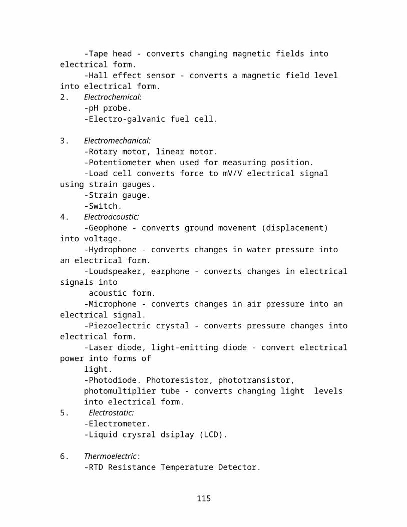
temperature equal numbers of charge carriers: electrons and holes are thermally generated, and it is these which give rise to the intrinsic conductivity.
Intrinsic semiconductor - Is a pure semiconductor in which the electrons and hole densities are equal under condition of thermal equilibrium. In practice absolute purity is unattainable and the term is applied to nearly pure materials.
Extrinsic semiconductor – Is asemiconductor in which the charge carrier concentration is dependent is dependent upon impurities or other imperfections.
Depletion layer: Is a space-charge region in a semiconductor in which there is a net charge due to insufficient mobile charge carriers. Depletion layers are formed, for example, at the interface between a p-type and n-type semiconductor in the absence of an applied field. They are also formed at the interface of a metal and a semiconductor.
Rectifier- Is an electrical device that permits current to flow in only one direction and can thus make alternating into direct current. It operates either by suppressing or attenuating alternate half-cycles of the current waveform or by reversing them. The most common rectifiers are semiconductor diodes.
Threshold voltage- Is the voltage at which a particular characteristic of an electric device first occurs. For an insulated-gate field-effect transistor, it is the voltage at which channel formation occurs.
Leakage- Is the flow of an electric current, due to imperfect insulation, in a path other than that intended.
Leakage current- Is a fault due to leakage. It is small in magnitude compared with that of a short circuit.
Amplifier- Is a device for reproducing an electrical input at an increased intensity. If an increased e.m.f.is produced operating into a high impedance, the device is a voltage amplifier, and if the output prodvides an appreciable current flow into a relativiely low impedance, the device is a power amplifier. The most commonly used amplifiers operate by transistors.
Logic circuit- Is a circuit designed to perform a particular logical function based on the concepts of “and”, “either-or”, etc. Normally these circuits operate between two discrete voltage levels, i.e. high and low logic levels, and are described as binary logic circuits. Logic using three or more logic levels is possible, but not common.
Logic gates- Is a device used to implement the elementary logic functions. These basic gates include among others: AND gate; Inverter (NOT gate); NAND gate; NOR gate…
115
Transducers- Is any device for converting a nonelectrical signals (or vice versa), the variations in the electrical signal being a function of the input. The transducers are used as measuring instruments and in the electroacoustic field, the term being applied to gramophone pick-ups, the microphones, and loudspeakers. The physical quantity measured by the transducer is the measurand, the portion of the transducer in which the output originates is the transducer elements, and the nature of the operation is the transduction principle. The device in the transducer that responds directly to the measurand is the sensing element and the upper and lower limits of the measurand value for which the trandsucer provides a useful output is the dynamic range.
Microprocessor- Is the integration of a number of useful functions into a single IC package. These functions are the ability to execute a stored set of instructions to carry out user defined tasks, and the ability to be able to access external memory chips to both read and write data from and to the memory.
XII. Compiled List of Compulsory Readings
Reading 1Complete reference: http://en.wikibooks.org/wiki/Electronics. 3rd October 2007.
Abstract: This is a complete textbook on electronics that deals with among others: analogue circuits: vacuum tubes; diodes, transistors; amplifiers; operational amplifiers, and analogue multipliers
Rationale: Each of the topic is presented in very simple form that makes it easier for one to read through. However, these simply serve to supplement the learning process.
Reading 2. Reference: http://en.wikipedia.org/wiki/electronics. 5th October 2007.Abstract: This reading is formed from references obtained from many sites. Their URLs can be obtained from a soft copy of this reading. Basically all the essential topics of the course are covered in this reading 2.Rationale. The reference provide easy reading sources on electronics that a reader should have no problem using them.
Reading 3: Operational Amplifier WIKIBOOKS
Reference: http://en.wikibooks.org/wiki/Electronics/Op-Amp. 5th October 2007.Abstract: Reading 3 include: Amplifiers, op-amp, notation, quick design process, ideal op-amps, basic op-amps configuration, advanced op-amp configurations and real op-amp.
116
Rationale: The provides most of the required on operational amplifier that is needed for the course.
Reading 4: Boolean Algebra + Notes on Designing simulation of Schmitt’sTrigger circuitReference: http://en.wikipedia.org/wiki/Electronics/Boolean-Algebra. 5th October 2007.Rationale: This provides easy reading materials on Boolean Algebra.
Reading 5: SensorsReference: http://Soundlab.cs.princeton.ed/learning/tutorials/sensors/node19.html. 7th July 2007.Abstract: the topics included are data acquisition (piezoelectric sensors, accelerometer, force sensing resistors, microphones, biopotential sensors); Signal conditioning (Requirements for A-D converters, voltage to voltage, current to voltage, resistance to voltage,, capacitance to voltage); data acquisition(anti aliasing, analogue to digital conversion, data acquisition systems).Rationale. This reading provides good materials on this activity.
Reading 7: Computers WIKIBOOKSReference: http://en.wikipedia.org/wiki/Computer. 4th October 2007.Abstract: The reference provides reading on stored programs architecture, and
how computer works. This includes control unit, arithmetic/logic unit (ALU), memory, input/output (I/O), multitasking, multiprocessing, andnetworking and internet.
Rationale: This provides a simple basic reading for someone beginning to learn about computer
XIII. Compiled List of Multimedia Resources Reference: http://www.educypedia.be/electronics/javacollectors.htmSummary: This resource enables a one to study Characteristics of NPN transistor Rationale: The site gives an elegant simple virtual experiment that one can carry to study the characteristics of NPN transistor.
Reference: http://server.oersted.dtu.dk/personal/ldn/javalab/Circuit04.htmlSummary: The resource is for circuit of a primitive common-emitter (CE) amplifier
comprising an npn-transistor and external basis-, collector- and load resistors. The learner will find for a fixed set of component parameters the ranges of input voltage that make the transistor cut off, active or saturated, respectively. In the case of analogue applications the learner will determine the differential voltage amplification of the circuit when the transistor is in the active range. While for digital applications one is expected to find the smallest possible current gain (beta) and a corresponding collector resistance
that makes the circuit a functional logical inverter.Rationale: This resource serves to aid one in learning about npn transisitor biasing.
Reference: http://server.oersted.dtu.dk/personal/ldn/javalab/Circuit01.html
117
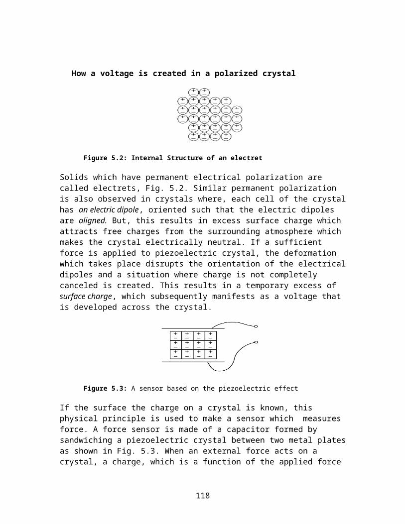
Summary: This resource gives a circuit of a Thevenin equivalent with a load in whichpower P is delivered to the load.
Rationale: This site provides a useful resource for learning about voltage divider.
Reference: http://jas.eng.buffalo.edu/education/semicon/fermi/bandAndLevel/index.html.
4th October 2007.Summary: The resource shows Fermi levels vs. carrier concentration and doping of donor and acceptor impurities.Rationale: The aids in the leaning of carrier concentration and doping of donor and
Reference: http://jas.eng.buffalo.edu/education/fab/BjtFet/index.html. 4th October 2007.Summary: The fabrication steps of a pair of Metal-Oxide-Semiconductor (MOS) Field Effect Transistor (FET) and a Bipolar Junction Transistor (BJT) on a Silicon wafer is illustrated in this applet. The four buttons, 'first', 'previous', 'next', and 'last' let you view the static images at various points of the device fabrication. The 'animate_next' button shows you through the animated 'time sequence' of the fabrication flow from this step to the next step. The animation capability teaches you most clearly the detailed physical steps involved. The fabrication steps of Semiconductor Devices involve many physical, chemical and thermal steps which this applet let you understand.Rational: This is a useful learning resource to use.
Reference: http://jas.eng.buffalo.edu/education/transistor/n_MOS_IV/mosfet.html. 4th October 2007.Summary: The resource shows an applet which calculates and plots the output characteristics of an n-channel (enhancement-mode) MOSFET. Try to change the drain-source voltage (Vds) range and/or the gate bias starting value ('begin') or other values and see the drain current vs. drain bias (Vds) change Rationale: This is a useful resource for one to learn hw to calculate and plot the output characteristics of an n-channel MSOFET.
Reference: http://server.oersted.dtu.dk/personal/ldn/javalab/Circuit03.html . 3rd October 2007.Summary: This resource is on inverting amplifier where the voltage source is turned on in order to check the circuit for different values of the resistances and/or the open-loop gain of the opampRationale: In the (normal) case of a large open-loop gain of the opamp (typically >100 dB) the feedback mechanism will force the inverting input terminal to be virtually grounded. In this limit the closed-loop amplification factor of the circuit will be determined solely by the resistance values.
Reference: http://jas.eng.buffalo.edu/ 3rd October 2007.Summary: Useful illustration of amplifiers with BJT and MOSFET are used to promote easy understanding of the topics
118
Rationale: Provides useful video about amplifiers with BJT or MOSFET -Circuit models of four basic amplifiers -Single-stage BJT amplifier circuits (CE, CB, and CC) -Single-stage common-emitter amplifier bias design (java1.1) -Single-stage MOSFET amplifier circuits (CS, CG and CD) -Different load types in an IC Amplifier Circuit (a CS amp example)
Reference: http://images.google.co.uk/images?hl=en&q=Transducers&oe=UTF-8&um=1&ie=UTF-8&sa=N&tab=wi. 4th October 2007.Summary: Images of different types of transducers are provided.Rationale: The resource is quite good as it provides one with information about the different transducers.
Reference: http://images.google.co.uk/images?hl=en&q=sensors&oe=UTF-8&um=1&ie=UTF-8&sa=N&tab=wi. 4th October 2007.
Summary: the resource provides different types of sensors.Rational: The images reinforces the learning when one looks at them.
Reference: http://www.eastaughs.fsnet.co.uk/cpu/index.htm. 7th October 2007.Summary: Topics covered include computer tutorial, microprocessor tutorial that discusses about CPP structure and instruction to executionRationale:. This provides concise illustration and explanation of a computer.
XIV. Compiled List of Useful Links Title: Basic circuit analysisURL: http://ocw.mit.edu/OcwWeb/Electrical-Engineering-and-Computer-Science/6-002Circuits-and-ElectronicsFall2000/VideoLectures/index.htm. 6th October 2007.Abstract: These contain the course lecture slides accompanying video lectures, and description of live demonstration shown by the instructor
Title: Diodes URL: http://jersey.uoregon.edu/~rayfrey/431/lab2_431.pdfhttp://jersey.uoregon.edu/Abstract: This site provides practical work V-I characteristics. In addition, the site
provides reading on transistor junctions, transistor switch and saturation etc.
Title: Diode applicationsURL: http://morley.eng.ua.edu/G332BW.pdf.Abstract: Various applications of diodes including power supply, half-wave rectifier,
bridge rectifier, full-wave rectifier with filter etc. are presented.
Title: MOSFET amplifierURL: http://ocw.mit.edu/OcwWeb/Electrical-Engineering-and-Computer-Science/6-002Circuits-and-ElectronicsFall2000/VideoLectures/index.htm. 4th October 2007.
119
Abstract: This contains the course lecture slides accompanying videos lectures, and description of live demonstration shown by instructor during lectures
Title: BJT and FET transistorURL: http://www.nhn.ou.edu/~bumm/ELAB/Lect_Notes/BJT_FET_transitors_v1_1.html.3rd October 2007.Abstract: This site provides good reading materials on BJT and FET transistor
Title: Bipolar junction transistorURL: "http://en.wikipedia.org/wiki/Common_collector. 4th October2007.Abstract: This provides very good reading materials on structure of NPN, PNP, heterojunction bipolar transistor, transistor circuits and applications of transistors.
Title: CMOSURL: "http://en.wikipedia.org/wiki/CMOS. 4th October 2007.Abstract: This site provides some good reading materials on structure of NAND gate, power switching, and leakage
Title: Common SourceURL: "http://en.wikipedia.org/wiki/Common_source. 4th October 2007.Abstract: This provides some reading on characteristics of bandwidth.
Title: JFETURL: "http://en.wikipedia.org/wiki/JFET”. 4th October 2007.Abstract: This is a source of good reading materials about JFET on the structure, function, schematic symbols, and comparison with other transistors
Title: Operational amplifierURL: http://ocw.mit.edu/OcwWeb/Electrical-Engineering-and-Computer-Science/6- 002Circuits-and-ElectronicsFall2000/VideoLectures/index.htm. 3rd October 2007.
Abstact: These contain course lecture slides accompanying video lectures, and descriptions of live demonstration shown by instructor during lectures
Title: OP-AmpsURL: "http://en.wikibooks.org/wiki/Electronics/Op-Amps". 4th October 2007.Abstract: Provides good reading materials on amplifiers, Op-Amp, notation, ideal Op-
Amps, basic Op-Amp configurations, and real Op-Amp.
Title: Operational AmplifierURL: "http://en.wikipedia.org/wiki/Operational_amplifier. 4th October 2007.
Abstract: This has good reading materials on operational amplifier. The topics include: basic operation, the ideal op-amp, limitations of real op-amps, notations, use of
120
electronics system design, DC behaviour, AC behaviour, Basic non-inverting amplifier circuit, internal circuitry of 741 type of op-amp, and common applications.
Title: Digital LogicURL: http://www.educypedia.be/electronics/digital.htm. 3rd October 2007.Abstract: This site provides reading materials on logic gates, Venn diagrams, de Morgan's theorems, combinatorial logic circuits, canonical forms, Boolean algebra, Karnaugh maps, truth tables, switch debouncing, JK flip-flop, master-slave flip-flop, binary subtraction, binary arithmetic, JK Flip-Flop, D latch, D Flip-Flop, Flip-Flop symbols, converting Flip-Flop inputs, alternate flip-flop circuits, D Flip-Flop; using NOR latches, CMOS Flip-Flop construction, counters, ripple counter.
Title: Schmitt’s triggerURL: http://www.visionics.ee/curriculum/Experiments/Schmitt%20Trigger/Schmitt%20Trigger1.html. 3rd October 2007.Abstract: This provides additional reading on the theory of Schmitt’s trigger.
Title: Logic GatesURL: http://www.shef.ac.uk/physics/teaching/phy107/phy107.htmlhttp://www.shef.ac.uk/physics/teaching/phy107/phy107.html. 3rd October 2007.
Abstract: This reading equips the student with the fundamental skills required in digital circuit design. No prior knowledge of digital techniques is assumed. The reading first introduces the basic logic gates which form the fundamental building blocks of all digital circuits. It then progresses to combine these circuit elements in a number of ways in order build circuits which provide certain functionalities such as counting and addition. Aspects
of circuit design are also covered.
Title: Boolean AlgebraURL: "http://en.wikibooks.org/wiki/Electronics/Boolean_Algebra. 4th October 2007.Abstract: Here formal mathematical operations are presented along with Boolean
algebra laws. In addition, a number of examples are given.
Title: MultiplexingURL: "http://en.wikipedia.org/wiki/Multiplexing. 4th October 2007.Abstract: The reading includes telegraphy, video processing, digital broadcasting,
and analogue broadcasting.
Title: PiezoelectricityURL: http://en.wikipedia.org/wiki/Piezoelectricity. 4th October 2007.Abstract: This provides useful reading on : materials, applications which includes high voltage and power sources, sensors, actuators, piezoelectric motors, and crystal classes.
Title: Transducers URL:. "http://en.wikipedia.org/wiki/Transducer"; 4th October 2007. Abstract: This provides good reading about types of transducers, which include among
121
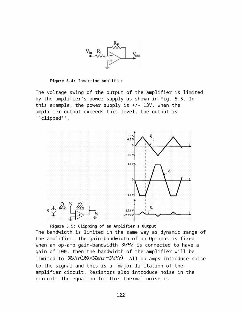
others: antenna, flourescent lamp, Hall effect sensor, rotary motor, vibration powered generator, piezoelectric crystal and photodiodes.
Title: ComputersURL: http://en.wikipedia.org/wiki/Computer 4th October 2007.Abstract: The resource provides reading on stored programs architecture, and how computer works. This includes control unit, arithmetic/logic unit (ALU), memory, input/output (I/O), multitasking, multiprocessing, and networking and internet.
Title: Microprocessor URL: http ://en.wikipedia.org/wiki/Microprocessor . 5th October 2007.Abstract: This providess some basic reading materials on: notable 8-bit designs, 16-bit
designs, 32-bit designs, and 64-bit designs in personal computers.
Title: 32-bit in computer architectureURL: http://en.wikipedia.org/wiki/32-bitAbstract: This gives the meaning of a 32-bit processor
Title: 8-bit in computer architecturehttp://en.wikipedia.org/wiki/8-bitAbstract. The topic includes list of 8 bits CPUs
XV. Synthesis of the Module As a starting point, devices like resistors, capacitors, and inductors are called linear components because the current increases in direct proportion to the applied voltage in accordance with Ohm’s law. However, we learnt that components like diodes, for which this proportionality does not hold are termed nonlinear devices, and that they are the basis for all practical electronic circuits. The key concepts that this activity provided was the examination of the properties of one of the nonlinear devices, the diode rectifier. Here the learning showed that a rectifier passes a greater current for one polarity of the applied voltage than the other. In addition, when a rectifier is included in an ac circuit, the current is negligible whenever the polarity of the voltage across the rectifier is in the reverse direction. The key principal applications considered the use of diodes in full wave rectification.
We also learnt that, the versatility inherent in nonlinear electronic components is enhanced immeasurably by the capability to influence current in the device in accordance with signals introduced at a constant electrode, which are considered active devices, because the control electrode permits active interaction with currents in the device. Principally, you encountered that, electrical properties of active devices are described by current-voltage characteristics. Basically, the current-voltage characteristics of electronics electronic devices depend primarily upon the motions of free electrons in them. Accordingly, the properties of transistors and other semiconductor devices, such as
122
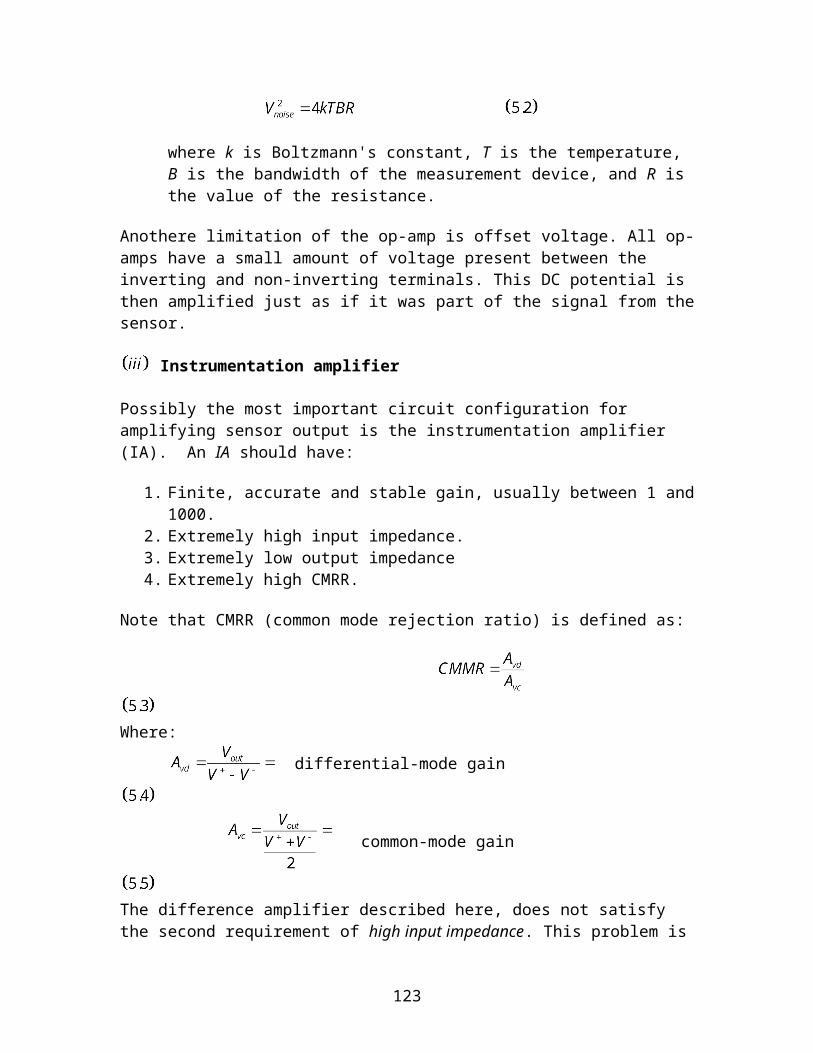
the junction diode, stem directly from the behaviour of electrons in semiconductor crystals. Different types and applications of of transistors were discussed and learnt in the module. Just like diodes, transistors are also nonlinear devices. Their operation is determined by graphical analysis using the description of their electrical properties given by current-voltage characteristics. The analysis differs in detail for voltage-controlled devices such as the field-effect transistor compared to current-controlled devices such as bipolar transistor, but is not different in principle.
In the module we saw that the performance of transistor amplifiers is enhanced in any respects by returning a fraction of the output signal to the input terminals. This process is called feedback. We saw that the feedback signal may either augment the input or tend to cancel it, and the latter, is called negative feedback. The learning activity showed that, improved frequency-response characteristics and reduced waveform distortion are attained with negative feedback. In addition, we saw that, amplifier performance is much less dependent upon change in transistor parameters caused by aging or temperature effects. The module discussion included a particular form of negative feedback, known as operational feedback used in amplifiers which perform mathematical operations such as addition or integration on an input signal. We saw that operational amplifiers are widely in measurement and control applications, as well as in electronic analog computers.In activity 4, we saw that numerical digits can be represented by electric signals which have only two possible magnitudes, say, zero and some finite value. In this situation we saw that, only the existence of one signal state or the other is significant, and the actual magnitude is relatively unimportant. That, digital circuits need have only two stable conditions represented by a transistor fully conducting, or completely cut off. Such circuits are inherently more reliable than those which must handle continuous range of signal levels. That any given number can be represented by a digital waveform so accuracy is not limited by the stability of circuit parameters. That, digital signals are manipulated by circuits according to specific logic statements which make possible exceedingly flexible and powerful processing of information. The module culminated into producing very complex digital processing logic on single chips. Such microprocessors use the techniques of digital computers which are used for several different applications.
XVI. Summative Evaluation 1. Discuss the operation of a PNP transistor
Describe how the static characteristics of a NPN transistor connected in the common-base configuration can be determined.A transistor operating in CB configuration has =3.0 mA, mA and = 0.02 mA. What current will flow in the collector circuit of this transistor when connected in CE configuration?
7. Show that in a CE configuration and have a relation given by
123
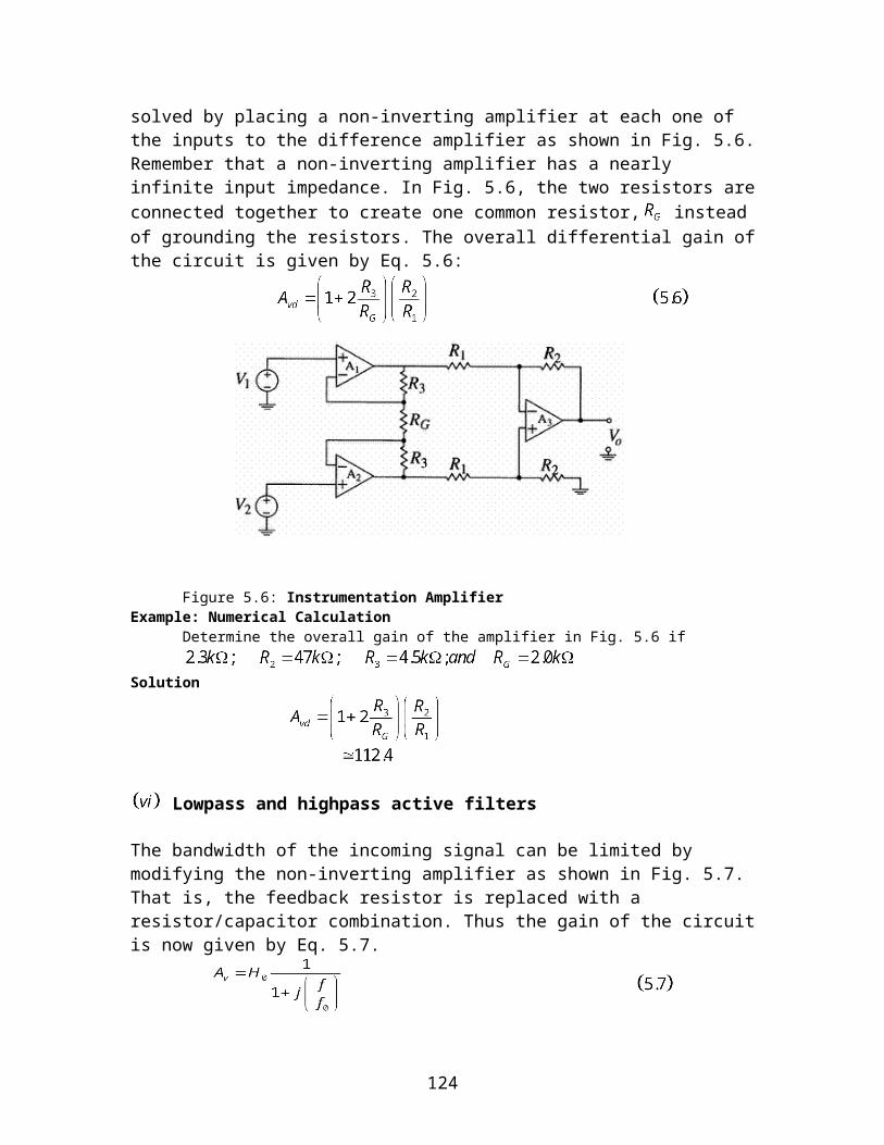
MN
3Q2Q1QA
1R 2R5V
X B
Discuss the origin of leakage current in a transistor
For a certain transistor, = 5.450 mA, . Find
the values of .
3. Use suitable examples to distinguish between intrinsic semiconductors and extrinsic semiconductorsFind the intrinsic carrier concentration in silicon at K for which
,
4. Explain the formation of depletion layer in a P-N junction.
With the use of suitable diagrams, describe a P-N junction in the forward mode.
5. Briefly describe the three essential parts through which information are processed: sensors, signal conditioning, and data acquisition 6. Briefly describe the working of a multiplexer and a decoder.
Find the number of input lines that can be coded to3. eight bit word4. sixteen bit word
7. Use the diagram below, to describe what takes place in a possible transistor OR gate consisting of three interconnected transistors Q1, Q2, and Q3 supplied from a common supply = +5V .
Construct a truth table for a 3-input AND gate
Design the equivalent electrical circuits for the AND gate.
8 Convert the binary fraction 0.101 into its decimal equivalent.
Use Double-Dadd Method and convert and convert 110012 to decimal
Cconvert 101011 into its octal equivalent.
124
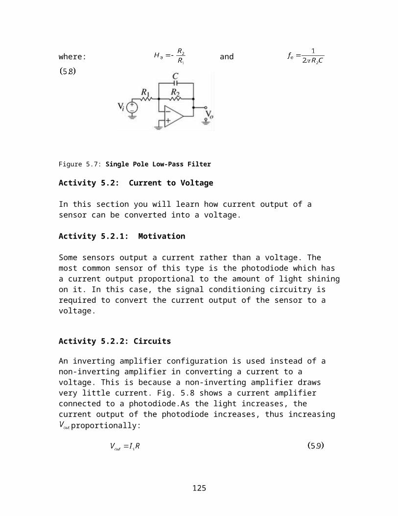
9. With the aid of suitable diagram describe the action of a JFET.
A field effect transistor having = 3 mA/V and =60 is used with a drain load resistance of 35 in a.f. voltage amplifier. Find the voltage gain.
10. Describe an Op-amps may be used as summing amplifier.
Show that the gain in a non-inverting amplifier is given by
XVII. References
1. Frederick F. Driscoll; Robert F. Coughlin. Solid State devices and Applications, D.B Taraporevala Sons & Co.PVT, Published with arrangement withPrentice Hall, Inc. 1981.
2. Bernard Grob, Basic Electronics, 4th ed., McGraw Hill International Book Company, London, 1983.
3. Close K.J & J Yarwood. Experimental Electronics for Students, London Chapman and Hall, Halsted Press Book, John Woley & Sons, 1179.
4. Tayal D.C. Basic Electronics. 2nd ed. Himalaya Publishing House Mumbai, 1998.5. Theraja B.L., R.S. Sedha. Principles of Electronic Devices and Circuits, S.Chand &
Company Ltd, New Delhi, 2004.6. Sparkes J.J. Semiconductor Devices 2nd ed. Chapman & Hall, London, 1994.7. Richard R. Spenser & Mohammed S. Ghaussi. Introduction to Electronic Circuit Design,
Prentice Hall, Pearson Education, Inc 2003.8. Noel M Morriss. Semiconductor Devices, MacMillan Publishers Ltd. 1984.9. Robert Boylestad& Louis Nashelsky. Electronic Devices and Circuit Theory, Prentice-Hall
International Editions. 1992.10. James J. Brophy. Basic Electronics for Scientists. 5th Edition, McGraw-Hill Publishing
Company, New York, 1990.
XVIII STUDENT RECORD
NAMEREGISTRATION No Assign 1 Assign. 2 Assign 3 Av. Assign Test 1 Test 2 Av. Test TOTAL
XVIII. Main Author of the Module
Dr. Obwoya Kinyera Sam is a Senior Lecturer in the Department of Physics at Kyambogo University, Uganda. He is currently the Director of Open Distance and e-Learning at Kyambogo University. He has
125
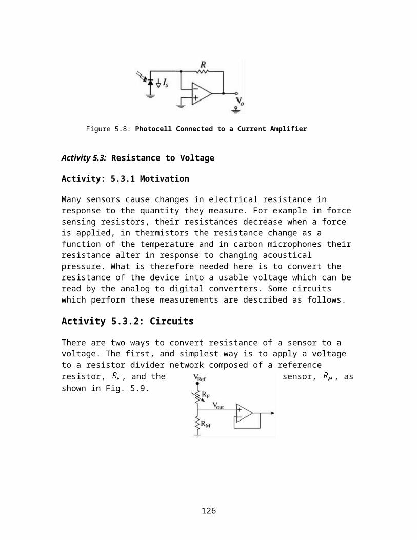
been a teacher educator since 1984. Between 1978 and 1984, he was Head of physics Department at Old Kampala Secondary school, in Uganda.His e-mail address is [email protected].
126