Embed Size (px)
DESCRIPTION
na
Citation preview
Leakage Current Reduction in VLSI Systems
David Blaauw, Steve Martin, *Krisztian Flautner, Trevor MudgeUniversity of Michigan, Ann Arbor, MI
*ARM Ltd, Cambridge, UK
Abstract
There is a growing need to analyze and optimize the stand-by component of power in digital circuits designed forportable and battery-powered applications. Since these circuits remain in stand-by (or sleep) mode significantlylonger than in active mode, their stand-by current, and not their active switching current, determines their batterylife. Hence, stringent specifications are being placed on the stand-by (or leakage) current drawn by such devices.As the power supply voltage is reduced, the threshold voltage of transistors is scaled down to maintain a constantswitching speed. Since reducing the threshold voltage increases the leakage of a device exponentially, leakagecurrent has become a dominant factor in the design of VLSI circuits. In this paper, we describe a method that usessimultaneous dynamic voltage scaling (DVS) and adaptive body biasing (ABB) to reduce the total power con-sumption of a processor under dynamic computational workloads. Analytical models of the leakage current,dynamic power, and frequency as a function of supply voltage and body bias are derived and verified with SPICEsimulation. Given these models, we show how to derive an analytical expression for the optimal trade-offbetween supply voltage and body bias, given a required clock frequency and duration of operation. The proposedmethod is then applied to a processor and is compared with DVS alone for workloads obtained using real-timemonitoring of processor utilization for four typical applications.
1. IntroductionPower consumption has become an overriding constraint for microprocessor designs, not only in mobile
environments, but in desktop and server applications as well. Traditionally, the supply voltage of microproces-
sors has been set at the maximum allowable voltage based on device breakdown potentials, and the processor is
run at maximum clock frequency. During typical use, however, the dynamic load of applications running on a
processor results in substantial periods of operation where the maximum performance of the processor is not
required. A number of methods have been proposed that take advantage of these periods of low utilization by
scaling the supply voltage and clock frequency, resulting in a reduction in dynamic power consumption [1-3].
While these dynamic voltage scaling (DVS) methods are effective in addressing the dynamic power con-
sumption, they are not as effective in reducing the leakage or static power. As minimum feature size continues to
shrink, the scaling of the maximum supply voltage requires a reduction in the threshold voltage which results in
an exponential increase of leakage current with each new technology generation. Even in today’s technologies, it
is not uncommon for leakage power to comprise as much as 20% of the total power consumption [4]. As technol-
ogies continue to scale, it is expected that leakage power consumption will become comparable to dynamic
power consumption [5]. Furthermore, during periods of low utilization, the lower clock frequency and lower cor-
responding voltage level result in reduced dynamic power consumption, thereby causing leakage power to dom-
inant.
1
For processors operating under dynamic computational loads, it is therefore essential that both leakage and
dynamic power are addressed effectively. Previously, adaptive reverse body biasing (ABB) has been proposed to
control the leakage current during standby mode [6-8]. Recently, methods using forward body biasing have also
been proposed [9,10]. Adaptive body biasing has the advantage that it reduces the leakage current exponentially,
whereas dynamic voltage scaling reduces leakage current linearly. In this paper, we propose the use of simulta-
neous dynamic voltage scaling and adaptive reverse body biasing to control both dynamic and leakage power.
The difficulty in employing simultaneous DVS and ABB is in determining the optimal trade-off between
supply voltage and reverse body bias voltage, such that the total power consumption at a particular frequency of
operation is minimized. The optimal trade-off between supply voltage and body voltage depends on the fre-
quency of operation, since this determines the relative magnitude of the dynamic and static power consumption.
The energy required for switching the supply voltage and the body voltage is amortized over the period of opera-
tion at a particular frequency. Since the switching energy for the body voltage and supply voltage differ, the opti-
mal trade-off therefore also depends on the length of the operation at a particular frequency. Finally, the possible
combinations of supply voltage and body-bias are constrained by the requirement that the circuit delay meets the
specified clock frequency.
In this paper, we derive an analytical expression for the optimal supply voltage and body voltage for a given
processor frequency and duration of operation. We present analytical models that express the power consumption
and processor performance as a function of the body voltage and supply voltage and show how to fit these func-
tions to SPICE simulation results with good accuracy. By using the performance of the processor as a constraint,
the resulting two dimensional optimization task is reduced to a one dimensional task and is solved through differ-
entiation. The analytical expression for the optimal supply voltage and body bias was verified through SPICE
simulations.
The proposed simultaneous DVS and ABB method was then applied to a processor and was compared with
using DVS alone. The dynamic processor loads were obtained through measurements on a 600MHz Crusoe pro-
cessor for four different applications. Expected gains from using simultaneous DVS and ABB were evaluated at a
current 0.18µm technology as well as for a projected 0.07µm technology. The simulations show that the proposed
method improves the total power consumption by an average of 23% for the 0.18µm process and by an average of
49% for the 0.07µm process. These substantial savings in total power result from the fact that for many applica-
tions, the processor spends substantial periods of time at very low performance levels where leakage current
dominates the total power consumption. The results also indicate that for future technologies with higher leakage
power, the effectiveness of the proposed method will increase.
The remainder of this paper is organized as follows. In Section 2, the models for dynamic power, leakage
power, and performance as a function of supply voltage and body bias are presented. In Section 3, we derive the
optimal trade-off point for the supply voltage and body bias. In Section 4 we apply these optimization techniques
to the Crusoe processor and in Section 5 we draw our conclusions.
2
2. Power and Performance ModelsWe first derive the threshold voltage as function of the supply and bias voltages and then express the total
power consumption as function of these voltages. We then derive the performance as a function of the supply and
body bias voltage. In all cases, we compare the analytical model to SPICE simulation results.
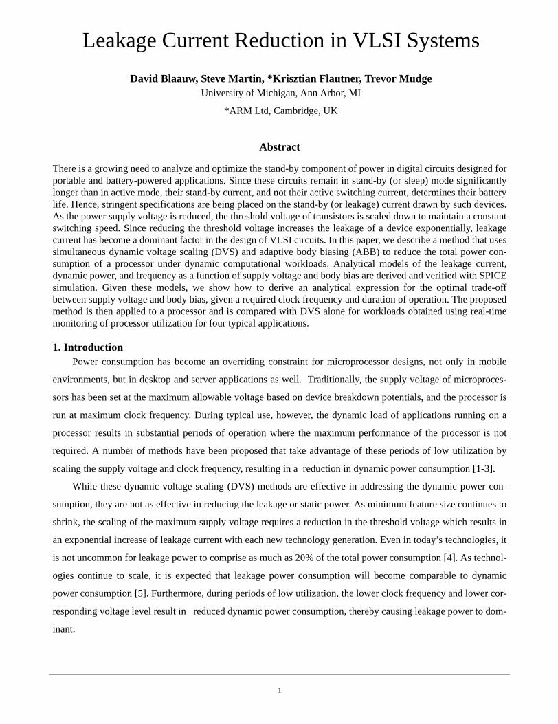
2.1 Threshold VoltageThe threshold voltage of a short-channel MOSFET transistor in the BSIM model [11,12] is given by,
(1)
where Vth0 is the zero-bias threshold voltage, Φs and γ are constants for a given technology, Vbs is the voltage
applied between the body and source of the transistor, ∆Vsce is the dependence of the threshold voltage on short
channel effects and drain induced barrier lowering, and ∆VNW is a constant for a given transistor size that models
narrow width effects. The change in threshold voltage due to short channel effects is given by,
(2)
where θ(DIBL) is a function dependent only on process dependent fitting parameters and effective length of the
transistor, θ(SCE) is approximately a constant, and Vdd is the supply voltage. Combining (1) and (2) shows that
Vth has a linear dependence with Vdd. If then can be linearized as which yields,
(3)
where K1, K2 and Vth1 are constant fitting parameters. Figure 1 shows the linear dependence of Vth versus Vdd and
Vbs as given by SPICE simulation of the Berkeley predictive models for a 0.07µm process [13]. A least squares
method linear regression of Vth vs. Vdd and Vbs matches with (3) with a regression coefficient, R2, of 0.997, where
an R2 value of 1 is a perfect linear fit.
Vth Vth0 γ Φs Vbs– ΦS–( ) ∆VSCE ∆VNW+ + +=
∆VSCE θ SCE( )–≈ θ DIBL( ) Vdd⋅–
Vbs Φs≈ Φs V– bs Φs– k Vbs⋅
Vth Vth1 K1 Vdd⋅ K2– Vbs⋅–=
Figure 1. Vth vs. both Vdd and Vbs as generated by SPICE simulation for a deep-submicron process.
Vdd(V)-Vbs(V)
Vth
(V)
3
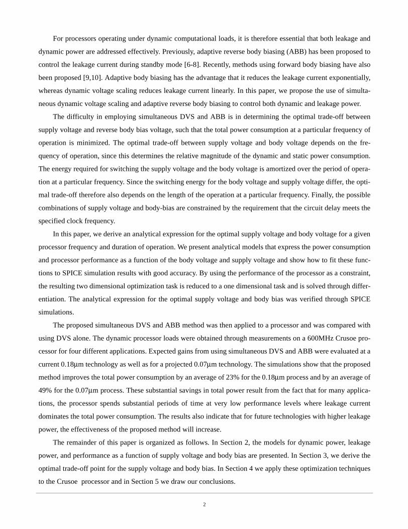
2.2 Power ConsumptionThe power consumed in a processor consists of three components as given by,
(4)
where PAC is the dynamic power, PDC is the static power due to leakage, and PSC is the negligible power due to
short circuits when both PMOS and NMOS devices are on during signal transitions [14]. The dynamic power is
given by,
(5)
where Ceff is the average switched capacitance per cycle, and f is the clock frequency. Figure 2 shows the major
components of static current in a standard inverter. Although [15,16] consider only the leakage due to Isubn and
Isubp, as [7,17] points out, the contributions of Ij and Ib can be significant. Thus, the static power consumption is
given by,
(6)
where Isubn is the subthreshold leakage current, Ijn is the drain to body junction leakage current, and Ibn is the
source to body junction leakage current through the NMOS device. Equation (6) is given for the inverter when its
output state is high (i.e. the NMOS device is leaking). A similar equation can be derived for the inverter when the
output state is low and the PMOS device is leaking.
The subthreshold leakage current through a transistor with Vds=Vdd and Vgs=0 is modeled by,
(7)
where W and L are the device geometries, Is, n, and Voff are empirically determined constants for a given process,
and VT is the thermal voltage [11]. Since Voff is typically small and is nearly 1 for all Vdd, (7)
can be approximated as,
(8)
where K3 and K4 are constant fitting parameters. Substitution of (3) into (8) yields,
P PAC PDC PSC+ +=
PAC Ceff Vdd2
f=
Vdd
GND
Vdd
GND
0 01 1
V+Vbs
-Vbs -Vbs
IjnIsubn
Ibn
Ijp
Isubp
Ibp
Vdd+Vbs
Figure 2. Static current sources for an inverter.
PDC VddIsubn Vbs Ijn( Ibn )+ +≈
IsubnWL-----
IS 1 e
Vdd–
VT
-----------
– eVth(– Voff )+
n VT
---------------------------------=
1 Vdd– VT⁄( )exp–
Isubn K3eK4Vth–
=
4
(9)
where K5 and K6 are constant fitting parameters. As |Vbs| is increased, the current due to junction leakage, Ij,
increases and counteracts the savings achieved by lowering Isubn. The maximum value of |Vbs| before junction
leakage overrides subthreshold current reduction is dependent on process and has been shown to vary from as
high as -0.6V to -2.5V [8,18]. This crossover point is also highly dependent on temperature, where at higher oper-
ating temperatures, transistors exhibit a larger reduction in Isubn (and thus tolerate a larger |Vbs|) before Ij
increases [8]. SPICE simulations for the 0.07µm process show that the crossover point is about -1.2V. Therefore,
to be safe, Vbs was constrained between 0 and -1V, although in a different process, a lower cutoff point might be
needed. Ij can be approximated as a constant,
(10)
and the total static current, Istat, becomes,
(11)
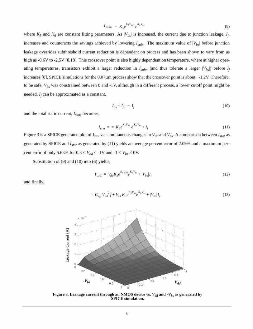
Figure 3 is a SPICE generated plot of Istat vs. simultaneous changes in Vdd and Vbs. A comparison between Istat as
generated by SPICE and Istat as generated by (11) yields an average percent error of 2.09% and a maximum per-
cent error of only 5.63% for 0.3 < Vdd < -1V and -1 < Vbs < 0V.
Substitution of (9) and (10) into (6) yields,
(12)
and finally,
(13)
Isubn K3eK5Vdd e
K6Vbs=
Ibn Ijn+ Ij=
Istat K3eK5Vdd e
K6Vbs Ij+==
Figure 3. Leakage current through an NMOS device vs. Vdd and -Vbs as generated by SPICE simulation.
Lea
kage
Cur
rent
(A
)
Vdd-Vbs
PDC VddK3eK5Vdde
K6Vbs Vbs Ij+=
Ceff Vdd2
f Vdd K3eK5Vdde
K6Vbs Vbs Ij++=
5
2.3 DelayThe delay of a gate is a function of both the power supply and the threshold voltage of the internal transis-
tors. Since the delay of complex gates remains proportional to the delay of a standard inverter, the circuit delay
can be modeled similarly to the alpha-power model of an inverter [19,20] as,
(14)
where K7 is a constant for a given process technology, and α is an indication of the amount of velocity saturation
occurring in the device (α is typically 1.3-1.5 for short channel devices). The critical path delay in a circuit can be
modeled as,
(15)
where tcrit is the delay of the critical path and Ld is the so-called logic depth of the path [15]. Substitution of (3)
and (14) into (15) yields,
(16)
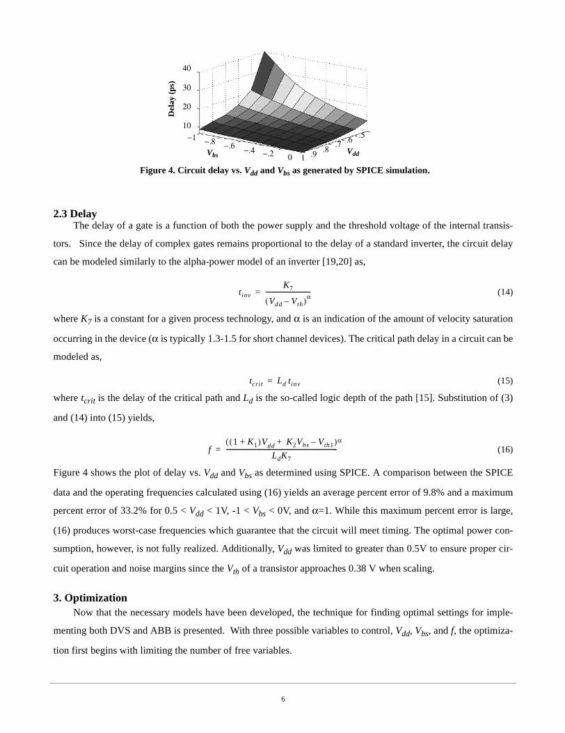
Figure 4 shows the plot of delay vs. Vdd and Vbs as determined using SPICE. A comparison between the SPICE
data and the operating frequencies calculated using (16) yields an average percent error of 9.8% and a maximum
percent error of 33.2% for 0.5 < Vdd < 1V, -1 < Vbs < 0V, and α=1. While this maximum percent error is large,
(16) produces worst-case frequencies which guarantee that the circuit will meet timing. The optimal power con-
sumption, however, is not fully realized. Additionally, Vdd was limited to greater than 0.5V to ensure proper cir-
cuit operation and noise margins since the Vth of a transistor approaches 0.38 V when scaling.
3. OptimizationNow that the necessary models have been developed, the technique for finding optimal settings for imple-
menting both DVS and ABB is presented. With three possible variables to control, Vdd, Vbs, and f, the optimiza-
tion first begins with limiting the number of free variables.
tinv
K7
Vdd Vth–( )α-----------------------------=
tcrit Ld tinv=
f1 K1+( )Vdd K2Vbs Vth1–+( )
LdK7
------------------------------------------------------------------------α
=
Figure 4. Circuit delay vs. Vdd and Vbs as generated by SPICE simulation.D
elay
(ps
)
VddVbs 0 1 .9 .8 .7 .6 .5
−.2−.4−.6−.8−110
20
30
40
6
3.1 Variable ReductionThe processor’s algorithm for determining utilization based on workload generates a value for the required
frequency eliminating one free variable. In order to eliminate a second variable, this frequency is treated as a con-
stant for a given optimization point and (16) can be solved to find Vdd as a function of Vbs. If α =1 then (16)
yields,
(17)
which may be rewritten as,
(18)
where, for a given frequency,
(19)
This leaves Vbs as the only free variable.
3.2 Energy MinimizationThe energy consumed per cycle is defined as,
(20)
By substituting in (13), the total energy consumed per cycle for an entire circuit is given by,
(21)
where Lg is the number of logic gates in the circuit. Unfortunately, there is also energy required in switching the
circuit between varying power modes. This switching energy, Es, is given by,
(22)
where ∆Vdd is the change in Vdd, ∆Vbs is the change in Vbs, Cr is the capacitance of the power rail, and Cs is the
total capacitance of the substrate and wells of the device. Let t be the duration of time in a given power mode
then the total energy consumed in a particular mode is given by,
(23)
Differentiating (23) with respect to Vbs yields,
(24)
where by substituting in (18),
dd
Ld K7 f K2Vbs– Vth1+
1 K1+----------------------------------------------------=
VddK8Vbs Kf1+ if Vdd >0.5
0.5 otherwise
=
K8
K2–
1 K1+--------------- ,= Kf1
Vth1 Ld K7 f+
1 K1+-------------------------------=
Ecyc Pf1–=
Ecyc CeffVdd2 Lgf 1– Vdd K3e
K5VddeK6Vbs Vbs Ij+( )+=
Es ∆Vdd2Cr ∆Vbs
2Cs+=
Etot Es t f Ecyc⋅ ⋅+=
Etot∂Vbs∂
-----------Es∂Vbs∂
---------- t f⋅( )Ecyc∂Vbs∂
-------------+=
7
(25)
and
(26)
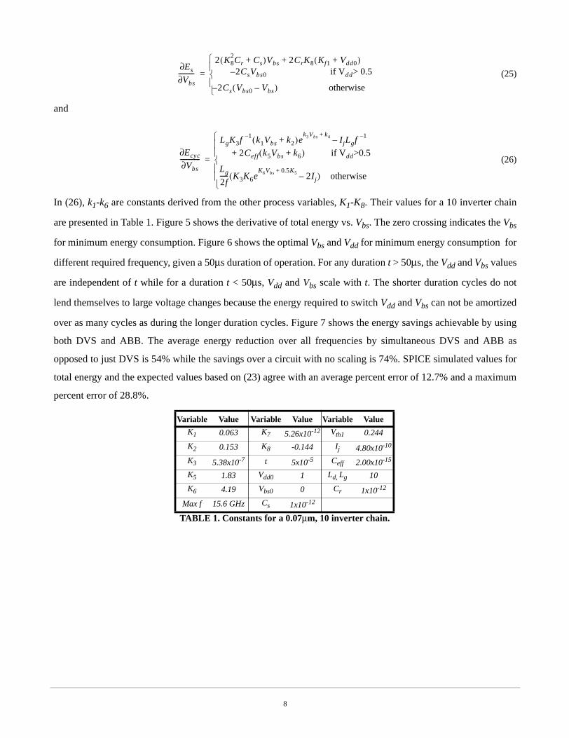
In (26), k1-k6 are constants derived from the other process variables, K1-K8. Their values for a 10 inverter chain
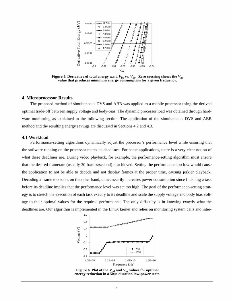
are presented in Table 1. Figure 5 shows the derivative of total energy vs. Vbs. The zero crossing indicates the Vbs
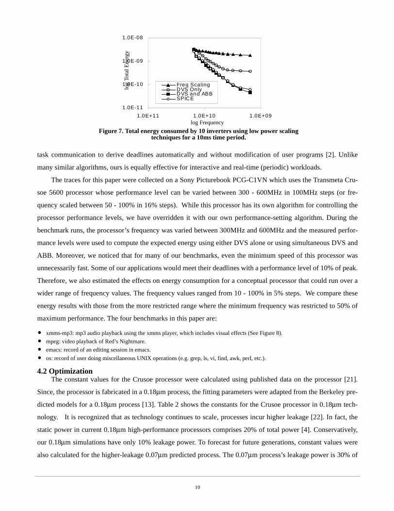
for minimum energy consumption. Figure 6 shows the optimal Vbs and Vdd for minimum energy consumption for
different required frequency, given a 50µs duration of operation. For any duration t > 50µs, the Vdd and Vbs values
are independent of t while for a duration t < 50µs, Vdd and Vbs scale with t. The shorter duration cycles do not
lend themselves to large voltage changes because the energy required to switch Vdd and Vbs can not be amortized
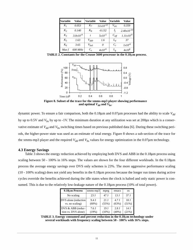
over as many cycles as during the longer duration cycles. Figure 7 shows the energy savings achievable by using
both DVS and ABB. The average energy reduction over all frequencies by simultaneous DVS and ABB as
opposed to just DVS is 54% while the savings over a circuit with no scaling is 74%. SPICE simulated values for
total energy and the expected values based on (23) agree with an average percent error of 12.7% and a maximum
percent error of 28.8%.
Es∂Vbs∂
----------
2 K82Cr Cs+( )Vbs 2CrK8 Kf1 Vdd0+( )+2CsVbs0– if Vdd> 0.5
2Cs Vbs0 Vbs–( )– otherwise
=
Ecyc∂Vbs∂
-------------
LgK3f 1– k1Vbs k2+( )ek3Vbs k4+
IjLgf 1––
2Ceff k5Vbs k6+( )+ if Vdd>0.5
Lg
2f----- K3K6e
K6Vbs 0.5K5+2Ij–( ) otherwise
=
Variable Value Variable Value Variable Value
K1 0.063 K7 5.26x10⁻¹² Vth1 0.244
K2 0.153 K8 -0.144 Ij 4.80x10⁻¹⁰
K3 5.38x10⁻⁷ t 5x10⁻⁵ Ceff 2.00x10⁻¹⁵
K5 1.83 Vdd0 1 Ld, Lg 10
K6 4.19 Vbs0 0 Cr 1x10-12
Max f 15.6 GHz Cs 1x10-12
TABLE 1. Constants for a 0.07µm, 10 inverter chain.
8
4. Microprocessor ResultsThe proposed method of simultaneous DVS and ABB was applied to a mobile processor using the derived
optimal trade-off between supply voltage and body-bias. The dynamic processor load was obtained through hard-
ware monitoring as explained in the following section. The application of the simultaneous DVS and ABB
method and the resulting energy savings are discussed in Sections 4.2 and 4.3.
4.1 WorkloadPerformance-setting algorithms dynamically adjust the processor’s performance level while ensuring that
the software running on the processor meets its deadlines. For some applications, there is a very clear notion of
what these deadlines are. During video playback, for example, the performance-setting algorithm must ensure
that the desired framerate (usually 30 frames/second) is achieved. Setting the performance too low would cause
the application to not be able to decode and not display frames at the proper time, causing jerkier playback.
Decoding a frame too soon, on the other hand, unnecessarily increases power consumption since finishing a task
before its deadline implies that the performance level was set too high. The goal of the performance-setting strat-
egy is to stretch the execution of each task exactly to its deadline and scale the supply voltage and body bias volt-
age to their optimal values for the required performance. The only difficulty is in knowing exactly what the
deadlines are. Our algorithm is implemented in the Linux kernel and relies on monitoring system calls and inter-
Figure 5. Derivative of total energy w.r.t. Vbs vs. Vbs. Zero crossing shows the Vbs value that produces minimum energy consumption for a given frequency.
-1.0E-11
-5.0E-12
0.0E+00
5.0E-12
1.0E-11
-0.4 -0.39 -0.38 -0.37 -0.36 -0.35 -0.34
11 GHz
9.4 GHz
8.6 GHz
7.8 GHz
7.0 GHz
6.2 GHz
5.5 GHz
4.7 GHz
Vbs
Der
ivat
ive
Tota
l Ene
rgy
(J/V
)
-1.2
-0.8
-0.4
0
0.4
0.8
1.2
1.0E+08 5.1E+09 1.0E+10 1.5E+10
VbsVdd
Vol
tage
(V
)
Frequency (Hz)
Figure 6. Plot of the Vdd and Vbs values for optimal energy reduction in a 50µs duration low-power state.
9
task communication to derive deadlines automatically and without modification of user programs [2]. Unlike
many similar algorithms, ours is equally effective for interactive and real-time (periodic) workloads.
The traces for this paper were collected on a Sony Picturebook PCG-C1VN which uses the Transmeta Cru-
soe 5600 processor whose performance level can be varied between 300 - 600MHz in 100MHz steps (or fre-
quency scaled between 50 - 100% in 16% steps). While this processor has its own algorithm for controlling the
processor performance levels, we have overridden it with our own performance-setting algorithm. During the
benchmark runs, the processor’s frequency was varied between 300MHz and 600MHz and the measured perfor-
mance levels were used to compute the expected energy using either DVS alone or using simultaneous DVS and
ABB. Moreover, we noticed that for many of our benchmarks, even the minimum speed of this processor was
unnecessarily fast. Some of our applications would meet their deadlines with a performance level of 10% of peak.
Therefore, we also estimated the effects on energy consumption for a conceptual processor that could run over a
wider range of frequency values. The frequency values ranged from 10 - 100% in 5% steps. We compare these
energy results with those from the more restricted range where the minimum frequency was restricted to 50% of
maximum performance. The four benchmarks in this paper are:
• xmms-mp3: mp3 audio playback using the xmms player, which includes visual effects (See Figure 8).
• mpeg: video playback of Red’s Nightmare.
• emacs: record of an editing session in emacs.
• os: record of user doing miscellaneous UNIX operations (e.g. grep, ls, vi, find, awk, perl, etc.).
4.2 OptimizationThe constant values for the Crusoe processor were calculated using published data on the processor [21].
Since, the processor is fabricated in a 0.18µm process, the fitting parameters were adapted from the Berkeley pre-
dicted models for a 0.18µm process [13]. Table 2 shows the constants for the Crusoe processor in 0.18µm tech-
nology. It is recognized that as technology continues to scale, processes incur higher leakage [22]. In fact, the
static power in current 0.18µm high-performance processors comprises 20% of total power [4]. Conservatively,
our 0.18µm simulations have only 10% leakage power. To forecast for future generations, constant values were
also calculated for the higher-leakage 0.07µm predicted process. The 0.07µm process’s leakage power is 30% of
1.0E-11
1.0E-10
1.0E-09
1.0E-08
1.0E+091.0E+101.0E+11
Freq ScalingDVS OnlyDVS and ABBSPICE
Figure 7. Total energy consumed by 10 inverters using low power scaling techniques for a 10ms time period.
log
Tota
l Ene
rgy
log Frequency
10
dynamic power. To ensure a fair comparison, both the 0.18µm and 0.07µm processes had the ability to scale Vdd
by up to 0.5V and Vbs by up to -1V. The minimum duration at any utilization was set at 200µs which is a conser-
vative estimate of Vdd and Vbs switching times based on previous published data [6]. During these switching peri-
ods, the higher-power state was used as an estimate of total energy. Figure 8 shows a sub-section of the trace for
the xmms-mp3 player and the required Vdd and Vbs values for energy optimization in the 0.07µm technology.
4.3 Energy SavingsTable 3 shows the energy reduction achieved by employing both DVS and ABB in the 0.18µm process using
scaling between 50 - 100% in 16% steps. The values are shown for the four different workloads. In the 0.18µm
process the average energy savings over DVS only schemes is 23%. The more aggressive performance scaling
(10 - 100% scaling) does not yield any benefits in the 0.18µm process because the longer run times during active
cycles override the benefits achieved during the idle states when the clock is halted and only static power is con-
sumed. This is due to the relatively low-leakage nature of the 0.18µm process (10% of total power).
Variable Value Variable Value Variable Value
K1 0.053 K7 51x10-12 Vth1 0.359
K2 0.140 K8 -0.132 Ij 2.40x10⁻¹⁰
K3 3.0x10⁻⁹ t 5x10⁻⁵ Ceff 1.11x10⁻⁹
K5 1.63 Vdd0 1.6 Ld 37
K6 3.65 Vbs0 0 Cr 1x10⁻⁶
Max f 600 MHz Cs 4x10⁻⁶ Lg 4x10⁶
TABLE 2. Constants for the Crusoe 5600 processor in the 0.18µm process.
Time (s)
Vol
tage
(V
)
Perf
orm
ance
(%
)
Vbs
Vdd
Freq
Figure 8. Subset of the trace for the xmms-mp3 player showing performance and optimal Vdd and Vbs.
0.18µm Process xmms-mp3 mpeg emacs os
No scaling 23 J 47 J 13 J 37 J
DVS alone (reduction vs. no scaling)
9.4 J (60%)
21 J (55%)
4.7 J (63%)
18 J (51%)
DVS & ABB (reduc-tion vs. DVS alone)
7.6 J (19%)
19 J (10%)
2.8 J (40%)
14 J (21%)
TABLE 3. Energy consumed and percent reduction in the 0.18µm technology under several workloads with frequency scaling between 50 - 100% with 16% steps.
11
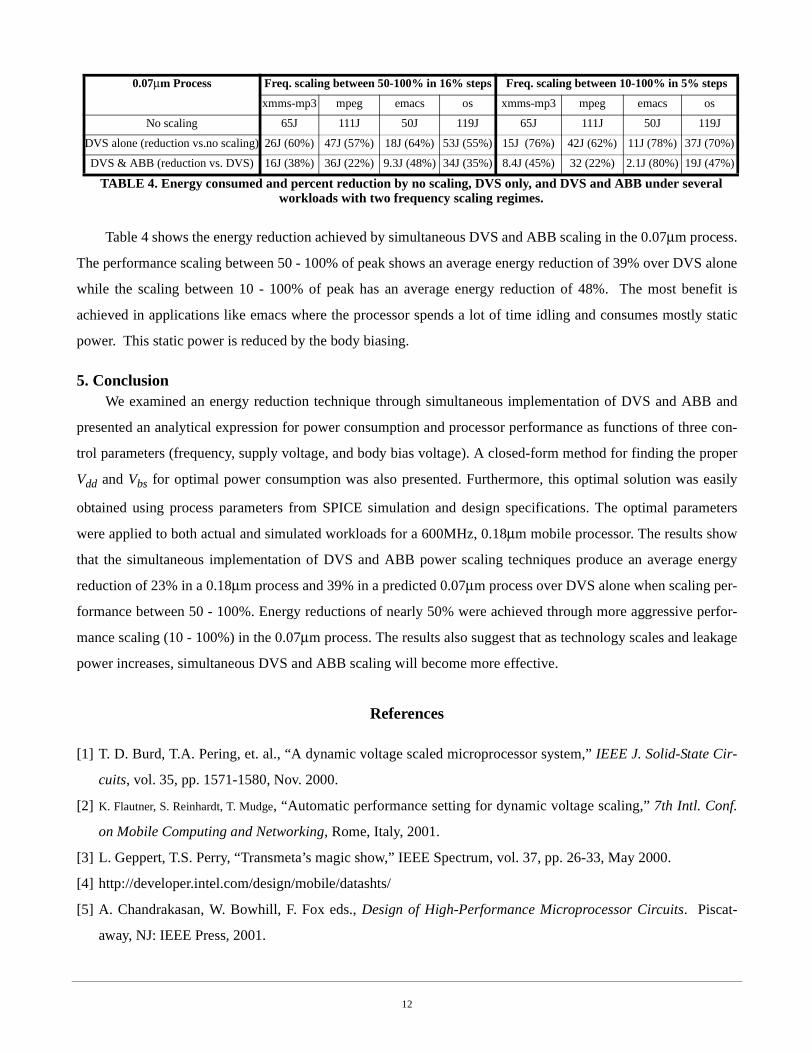
Table 4 shows the energy reduction achieved by simultaneous DVS and ABB scaling in the 0.07µm process.
The performance scaling between 50 - 100% of peak shows an average energy reduction of 39% over DVS alone
while the scaling between 10 - 100% of peak has an average energy reduction of 48%. The most benefit is
achieved in applications like emacs where the processor spends a lot of time idling and consumes mostly static
power. This static power is reduced by the body biasing.
5. ConclusionWe examined an energy reduction technique through simultaneous implementation of DVS and ABB and
presented an analytical expression for power consumption and processor performance as functions of three con-
trol parameters (frequency, supply voltage, and body bias voltage). A closed-form method for finding the proper
Vdd and Vbs for optimal power consumption was also presented. Furthermore, this optimal solution was easily
obtained using process parameters from SPICE simulation and design specifications. The optimal parameters
were applied to both actual and simulated workloads for a 600MHz, 0.18µm mobile processor. The results show
that the simultaneous implementation of DVS and ABB power scaling techniques produce an average energy
reduction of 23% in a 0.18µm process and 39% in a predicted 0.07µm process over DVS alone when scaling per-
formance between 50 - 100%. Energy reductions of nearly 50% were achieved through more aggressive perfor-
mance scaling (10 - 100%) in the 0.07µm process. The results also suggest that as technology scales and leakage
power increases, simultaneous DVS and ABB scaling will become more effective.
References
[1] T. D. Burd, T.A. Pering, et. al., “A dynamic voltage scaled microprocessor system,” IEEE J. Solid-State Cir-
cuits, vol. 35, pp. 1571-1580, Nov. 2000.
[2] K. Flautner, S. Reinhardt, T. Mudge, “Automatic performance setting for dynamic voltage scaling,” 7th Intl. Conf.
on Mobile Computing and Networking, Rome, Italy, 2001.
[3] L. Geppert, T.S. Perry, “Transmeta’s magic show,” IEEE Spectrum, vol. 37, pp. 26-33, May 2000.
[4] http://developer.intel.com/design/mobile/datashts/
[5] A. Chandrakasan, W. Bowhill, F. Fox eds., Design of High-Performance Microprocessor Circuits. Piscat-
away, NJ: IEEE Press, 2001.
0.07µm Process Freq. scaling between 50-100% in 16% steps Freq. scaling between 10-100% in 5% steps
xmms-mp3 mpeg emacs os xmms-mp3 mpeg emacs os
No scaling 65J 111J 50J 119J 65J 111J 50J 119J
DVS alone (reduction vs.no scaling) 26J (60%) 47J (57%) 18J (64%) 53J (55%) 15J (76%) 42J (62%) 11J (78%) 37J (70%)
DVS & ABB (reduction vs. DVS) 16J (38%) 36J (22%) 9.3J (48%) 34J (35%) 8.4J (45%) 32 (22%) 2.1J (80%) 19J (47%)
TABLE 4. Energy consumed and percent reduction by no scaling, DVS only, and DVS and ABB under several workloads with two frequency scaling regimes.
12
[6] H. Mizuno, K. Ishibashi, T. Shimura, T. Hattori, S. Narita, K. Shiozawa, S. Ikeda, K. Uchiyama, “A 18uA-
Standby-Current 1.8V 200MHz Microprocessor with Self Substrate-Biased Data-Retention Mode,” Proc.
IEEE International Solid-State Circuits Conference, pp.280-281, 1999.
[7] A. Keshavarzi, S. Narendra, et. al., “Effectiveness of reverse body bias for leakage control in scaled dual Vt
CMOS ICs,” Intl. Symp. on Low Power Electronics and Design, 2001.
[8] X. Liu, S. Mourad, “Performance of submicron CMOS devices and gates with substrate biasing,” IEEE Intl.
Symp. Circuits and Systems, Geneva, Switzerland, May 28-31.
[9] M. Miyazaki, J. Kao, A. Chandrakasan, “A 175mV Multiply-Accumulate Unit using an Adaptive Supply
Voltage and Body Bias Architecture,” IEEE Intl. Solid-State Circuits Conf., pp.58-59, 2002.
[10]S. Narendra, M. Haycock, et. al., “1.1V 1GHz Communications router with On-Chip Body Bias in 150nm
CMOS,” IEEE Int. Solid-State Circuits Conf, pp. 270-271, 2002.
[11]P. Ko, J. Huang, et. al., “BSIM3 for Analog and Digital Circuit Simulation,” Proc. IEEE Symposium on VLSI
Technology CAD, pp. 400-429, Jan. 1993.
[12]Z.H. Liu, C. Hu, J.H. Huang, et. al., “Threshold voltage model for deep-submicrometer MOSFETs,” IEEE
Tran. Electron Devices, vol. 40, pp. 86-95, 1993.
[13]http://www-device.eecs.berkeley.edu/~ptm/introduction.html
[14]H. Veendrick, “Short-circuit dissipation of static CMOS circuitry and its impact on the design of buffer cir-
cuits,” IEEE J. Solid-State Circuits, vol. 19, pp. 468-473, Aug. 1984.
[15]R. Gonzalez, et.al., “Supply and Threshold Voltage Scaling for Low Power CMOS,” IEEE J. Solid-State Cir-
cuits, vol. 32, pp. 1210-1216, Aug. 1997.
[16]M.R. Stan, “Optimal Voltages and Sizing for Low Power,” Intl. VLSI Design Conf., Goa, India, Jan. 1999.
[17]M. Chen, H. Huang, et. al., “Back-gate bias enhanced band-to-band tunneling leakage in scaled MOSFETS,”
IEEE Electron Device Letters, vol. 19, no. 4, pp. 134-136, Apr. 1998.
[18]A. Kesharvarzi, S. Narenda, et. al., “Technology scaling behavior of optimum reverse body bias for standby
leakage power reduction in CMOS ICs,” Intl. Symp. on Low Power Electronics and Design, pp. 252-254,
1999.
[19]T. Sakurai, A.R. Newton, “Alpha-power law MOSFET model and its applications to CMOS inverter,” IEEE
J. Solid-State Circuits, vol. 25, no. 2, pp. 584-594, Apr. 1990.
[20]K.A. Bowman, B.L. Austin, et. al., “A physical alpha-power law MOSFET model,” IEEE J. Solid-State Cir-
cuits, vol. 34, pp. 1410 -1414, Oct. 1999.
[21]http://www.transmeta.com/pdf/specifications/productbrief_tm5600_02aug00.pdf
[22]S. Thompson, P. Packan, and M. Bohr, “MOS Scaling: Transistor Challenges for the 21st Century.” Intel
Technology Journal, Q3 1998.
13


