Embed Size (px)
Citation preview
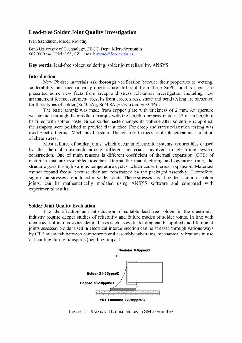
Lead-free Solder Joint Quality Investigation Ivan Szendiuch, Marek Novotný
Brno University of Technology, FECC, Dept. Microelectronics 602 00 Brno, Udolní 53, CZ email: [email protected] Key words: lead-free solder, soldering, solder joint reliability, ANSYS Introduction New Pb-free materials ask thorough verification because their properties as wetting, solderability and mechanical properties are different from these SnPb. In this paper are presented some new facts from creep and stress relaxation investigation including new arrangement for measurement. Results from creep, stress, shear and bend testing are presented for three types of solder (Sn/3.5Ag, Sn/3.8Ag/0.7Cu and Sn/37Pb). The basic sample was made from copper plate with thickness of 2 mm. An aperture was created through the middle of sample with the length of approximately 2/3 of its length to be filled with solder paste. Since solder paste changes its volume after soldering is applied, the samples were polished to provide flat surface. For creep and stress relaxation testing was used Electro-thermal Mechanical system. This enables to measure displacement as a function of shear stress. Most failures of solder joints, which occur in electronic systems, are troubles caused by the thermal mismatch among different materials involved in electronic system construction. One of main reasons is different coefficient of thermal expansion (CTE) of materials that are assembled together. During the manufacturing and operation time, the structure goes through various temperature cycles, which cause thermal expansion. Materiasl cannot expand freely, because they are constrained by the packaged assembly. Thereofore, significant stresses are induced in solder joints. These stresses creaating destruction of solder joints, can be mathematically modeled using ANSYS software and compared with experimental results. Solder Joint Quality Evaluation The identification and introduction of suitable lead-free solders in the electronics industry require deeper studies of reliability and failure modes of solder joints. In line with identified failure modes accelerated tests such as cyclic loading can be applied and lifetime of joints assessed. Solder used in electrical interconnection can be stressed through various ways by CTE mismatch between components and assembly substrates, mechanical vibrations in use or handling during transports (bending, impact).
Figure 1: X-axis CTE mismatches in SM assemblies
The main variables in assessment of material lifetime are strain and stress. Strain is simply a relative displacement of material particles per unit length and stress is a force per unit area generated by the relative displacement of various components. The stress generated by applied strain can result in elastic and/or plastic deformations. All elastic and some plastic deformation happen instantaneously. Most of the plastic deformation in solders develops with time and it is called creep strain, which is a function of applied stress. If the resultant stress occurs due to the application of a fixed strain the accumulated stress naturally decreases with time, this behavior is called stress relaxation and is expressed as a function of the strain initially applied (i.e. behavior of material after a strain is reached). The materials data for solders in the literature has been measured on dumb bell sized samples with a gauge diameter of a few millimeters. Today’s electronic assemblies have joints that are measured in microns, and hence are a few multiples of the grain size. What means the quality of solder joint and how to evaluate it? The solder joint quality is often uptake as general term without concrete definition simply evaluated on the base of subjective discussion. Before considering the criteria of solder joint quality, solder joint design and solder pads on substrate must be corresponding. Then we can put two questions, what the measurable criteria are and how to measure them to say this concrete solder joint is good or poor quality. There are three fundamental criteria to achieve final results for solder joint quality evaluation by visual inspection:
• The wetting of the solder pad surface • The shape of solder joint (depending on the amount of solder) • The condition of solder surface (color and smoothness)
Basic Approach to Solder Joint Quality
Solder joint quality can be judged in different point of views. In functional point joint life is the decisive parameter. It is time, when reliable function that means necessary conductivity is warranted. The most important factors influencing solder joint life are:
a) material ageing b) stress (mechanical) c) thermal stress
Ad a) The soldered joint represents heterogeneous dynamic system whose approximate constitution can be determined in this way: 75% solder 20% contact area on substrate (pad) 5% component outlet (contact)
Although individual components’ percentage is rather dissimilar, their influence on joint reliability could be nearly the same. That means it is necessary to focus on all three components. Basic task is how to determine the joint life or more precisely how long life can be warranted for given application. Joint life can be perceived as time when reliable function is warranted. It was approved than soldered joint ageing is mostly influenced by diffusion layer generated on boundary between tin and copper as can be seen in Figure 2. This layer affirms that soldered joint has been created but on the other side it is dangerous because of property deterioration, whether resistance increase or mechanical failure. Diffusion layer consists by SnPb solder compounds of intermetallic alloys Cu6Sn5 and Cu3Sn above all, which property is
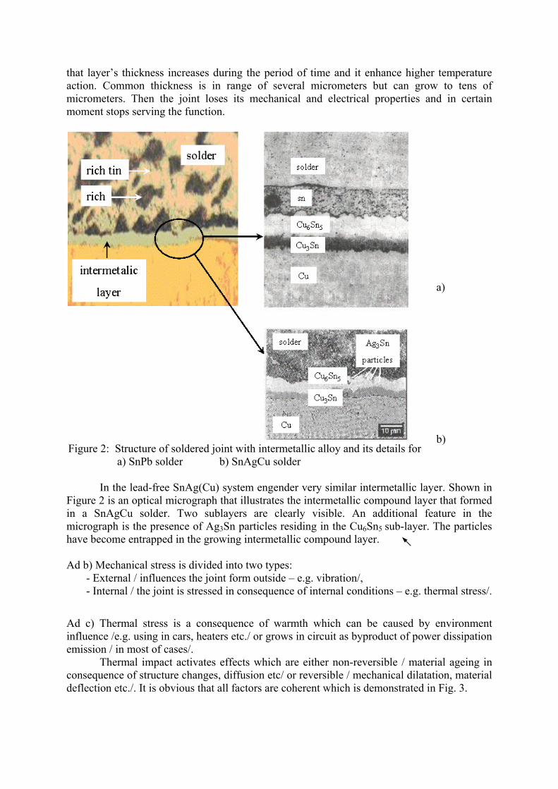
that layer’s thickness increases during the period of time and it enhance higher temperature action. Common thickness is in range of several micrometers but can grow to tens of micrometers. Then the joint loses its mechanical and electrical properties and in certain moment stops serving the function.
Figure 2: Structure of soldered joint with intermetallic alloy and its details for a) SnPb solder b) SnAgCu solder
In the lead-free SnAg(Cu) system engender very similar intermetallic layer. Shown in Figure 2 is an optical micrograph that illustrates the intermetallic compound layer that formed in a SnAgCu solder. Two sublayers are clearly visible. An additional feature in the micrograph is the presence of Ag3Sn particles residing in the Cu6Sn5 sub-layer. The particles have become entrapped in the growing intermetallic compound layer. Ad b) Mechanical stress is divided into two types: - External / influences the joint form outside – e.g. vibration/, - Internal / the joint is stressed in consequence of internal conditions – e.g. thermal stress/.
Ad c) Thermal stress is a consequence of warmth which can be caused by environment influence /e.g. using in cars, heaters etc./ or grows in circuit as byproduct of power dissipation emission / in most of cases/. Thermal impact activates effects which are either non-reversible / material ageing in consequence of structure changes, diffusion etc/ or reversible / mechanical dilatation, material deflection etc./. It is obvious that all factors are coherent which is demonstrated in Fig. 3.
a)
b)
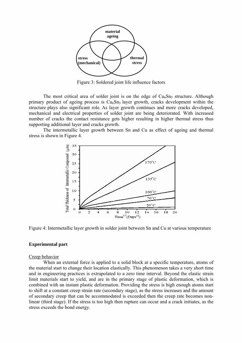
Figure 3: Soldered joint life influence factors
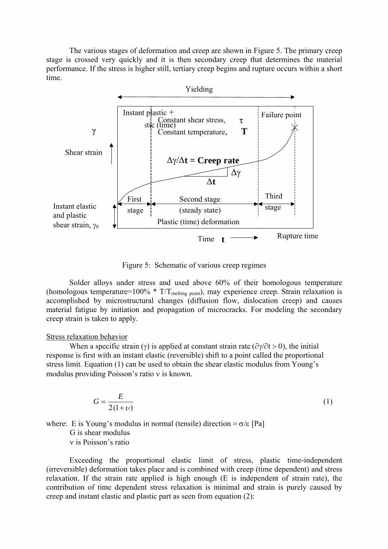
The most critical area of solder joint is on the edge of Cu6Sn5 structure. Although
primary product of ageing process is Cu6Sn5 layer growth, cracks development within the structure plays also significant role. As layer growth continues and more cracks developed, mechanical and electrical properties of solder joint are being deteriorated. With increased number of cracks the contact resistance gets higher resulting in higher thermal stress thus supporting additional layer and cracks growth.
The intermetallic layer growth between Sn and Cu as effect of ageing and thermal stress is shown in Figure 4.
Figure 4: Intermetallic layer growth in solder joint between Sn and Cu at various temperature
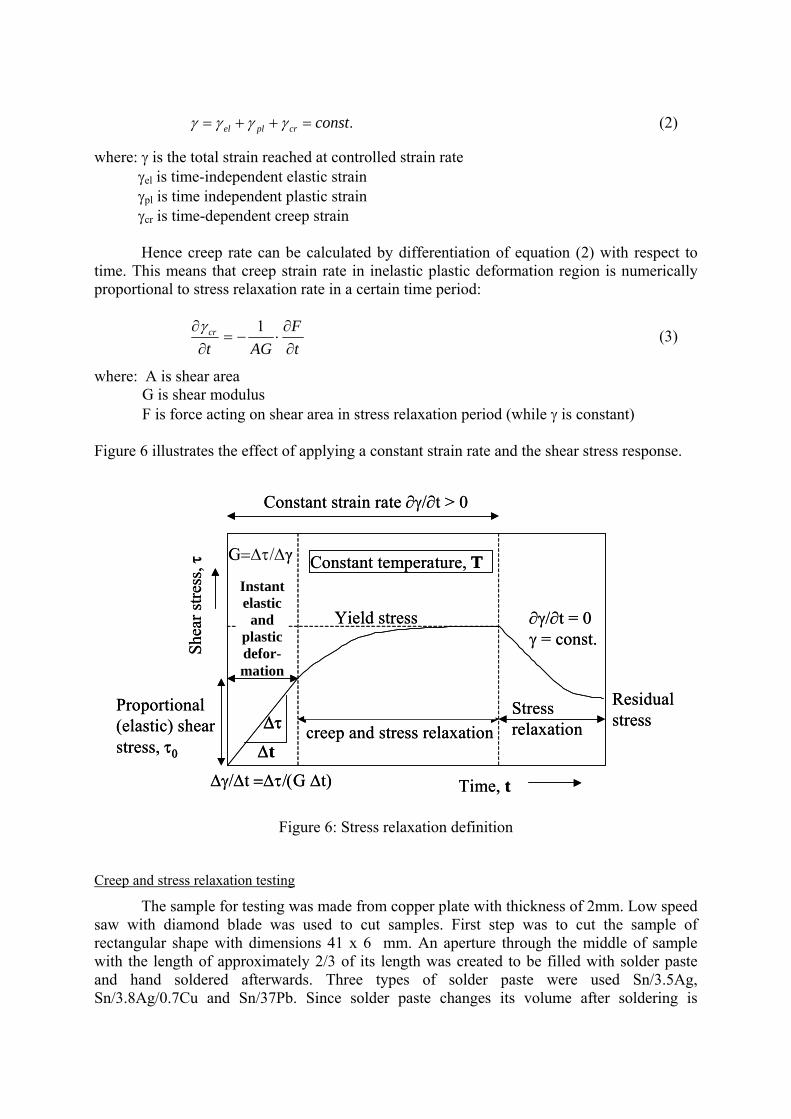
Experimental part Creep behavior When an external force is applied to a solid block at a specific temperature, atoms of the material start to change their location elastically. This phenomenon takes a very short time and in engineering practices is extrapolated to a zero time interval. Beyond the elastic strain limit materials start to yield, and are in the primary stage of plastic deformation, which is combined with an instant plastic deformation. Providing the stress is high enough atoms start to shift at a constant creep strain rate (secondary stage), as the stress increases and the amount of secondary creep that can be accommodated is exceeded then the creep rate becomes non-linear (third stage). If the stress is too high then rupture can occur and a crack initiates, as the stress exceeds the bond energy.
material ageing
thermal stress
stress (mechanical)
The various stages of deformation and creep are shown in Figure 5. The primary creep stage is crossed very quickly and it is then secondary creep that determines the material performance. If the stress is higher still, tertiary creep begins and rupture occurs within a short time.
Figure 5: Schematic of various creep regimes
Solder alloys under stress and used above 60% of their homologous temperature (homologous temperature=100% * T/Tmelting point), may experience creep. Strain relaxation is accomplished by microstructural changes (diffusion flow, dislocation creep) and causes material fatigue by initiation and propagation of microcracks. For modeling the secondary creep strain is taken to apply. Stress relaxation behavior
When a specific strain (γ) is applied at constant strain rate (∂γ/∂t > 0), the initial response is first with an instant elastic (reversible) shift to a point called the proportional stress limit. Equation (1) can be used to obtain the shear elastic modulus from Young’s modulus providing Poisson’s ratio ν is known.
)1(2 υ+
=EG (1)
where: E is Young’s modulus in normal (tensile) direction = σ/ε [Pa] G is shear modulus ν is Poisson’s ratio
Exceeding the proportional elastic limit of stress, plastic time-independent (irreversible) deformation takes place and is combined with creep (time dependent) and stress relaxation. If the strain rate applied is high enough (E is independent of strain rate), the contribution of time dependent stress relaxation is minimal and strain is purely caused by creep and instant elastic and plastic part as seen from equation (2):
Time t Rupture time
Shear strain
γ
Instant elastic shear strain, γ0
Constant shear stress, τConstant temperature, T
Firststage
Third stage
∆γ/∆t = Creep rate
Second stage (steady state)
∆t∆γ
Yielding
Failure point Instant plastic + plastic (time)
Plastic (time) deformation
Instant elastic and plastic shear strain, γ0
.constcrplel =++= γγγγ (2)
where: γ is the total strain reached at controlled strain rate γel is time-independent elastic strain γpl is time independent plastic strain γcr is time-dependent creep strain
Hence creep rate can be calculated by differentiation of equation (2) with respect to time. This means that creep strain rate in inelastic plastic deformation region is numerically proportional to stress relaxation rate in a certain time period:
tF
AGtcr
∂∂
⋅−=∂
∂ 1γ (3)
where: A is shear area G is shear modulus F is force acting on shear area in stress relaxation period (while γ is constant) Figure 6 illustrates the effect of applying a constant strain rate and the shear stress response.
Time, t
Shea
r stre
ss, τ
Proportional (elastic) shear stress, τ0
Constant temperature, T
Stress relaxation
Constant strain rate ∂γ/∂t > 0
Elas
tic
defo
rmat
ion
Instant plastic deformation+
creep and stress relaxation
G=∆τ/∆γ
∆t
∆τ
∆γ/∆t =∆τ/(G ∆t)
∂γ/∂t = 0γ = const.
Residual stress
Yield stress
Time, t
Shea
r stre
ss, τ
Proportional (elastic) shear stress, τ0
Constant temperature, T
Stress relaxation
Constant strain rate ∂γ/∂t > 0
Elas
tic
defo
rmat
ion
Instant plastic deformation+
creep and stress relaxation
G=∆τ/∆γ
∆t
∆τ
∆γ/∆t =∆τ/(G ∆t)
∂γ/∂t = 0γ = const.
Residual stress
Yield stress
Figure 6: Stress relaxation definition
Creep and stress relaxation testing
The sample for testing was made from copper plate with thickness of 2mm. Low speed saw with diamond blade was used to cut samples. First step was to cut the sample of rectangular shape with dimensions 41 x 6 mm. An aperture through the middle of sample with the length of approximately 2/3 of its length was created to be filled with solder paste and hand soldered afterwards. Three types of solder paste were used Sn/3.5Ag, Sn/3.8Ag/0.7Cu and Sn/37Pb. Since solder paste changes its volume after soldering is
Instant elastic
and plastic defor-mation
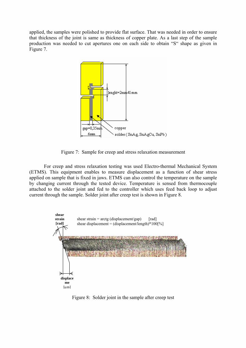
applied, the samples were polished to provide flat surface. That was needed in order to ensure that thickness of the joint is same as thickness of copper plate. As a last step of the sample production was needed to cut apertures one on each side to obtain “S“ shape as given in Figure 7.
Figure 7: Sample for creep and stress relaxation measurement
For creep and stress relaxation testing was used Electro-thermal Mechanical System
(ETMS). This equipment enables to measure displacement as a function of shear stress applied on sample that is fixed in jaws. ETMS can also control the temperature on the sample by changing current through the tested device. Temperature is sensed from thermocouple attached to the solder joint and fed to the controller which uses feed back loop to adjust current through the sample. Solder joint after creep test is shown in Figure 8.
Figure 8: Solder joint in the sample after creep test
displaceme
[µm]
shear strain [rad]
shear strain = arctg (displacement/gap) [rad] shear displacement = (displacement/length)*100[%]
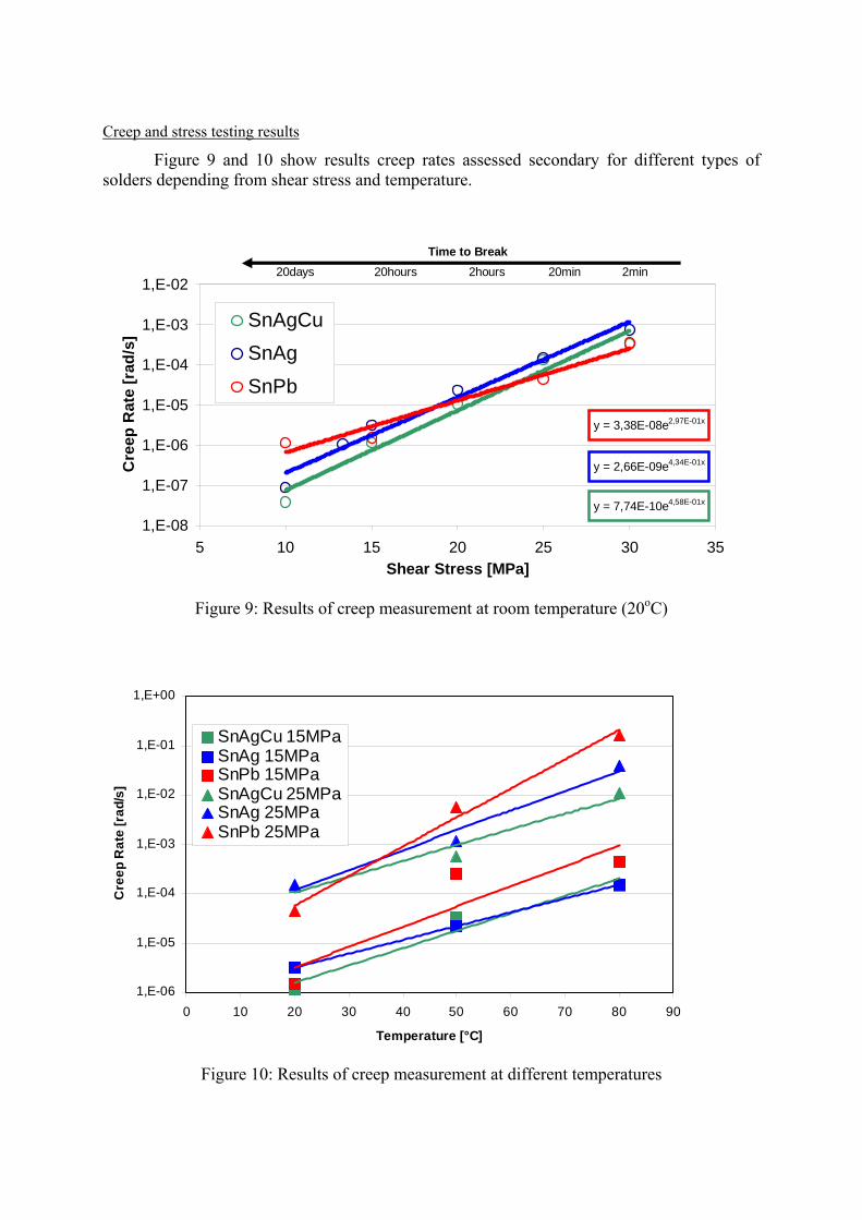
Creep and stress testing results
Figure 9 and 10 show results creep rates assessed secondary for different types of solders depending from shear stress and temperature.
y = 7,74E-10e4,58E-01x
y = 2,66E-09e4,34E-01x
y = 3,38E-08e2,97E-01x
1,E-08
1,E-07
1,E-06
1,E-05
1,E-04
1,E-03
1,E-02
5 10 15 20 25 30 35Shear Stress [MPa]
Cre
ep R
ate
[rad
/s]
SnAgCuSnAgSnPb
Time to Break20days 20min2hours20hours 2min
Figure 9: Results of creep measurement at room temperature (20oC)
1,E-06
1,E-05
1,E-04
1,E-03
1,E-02
1,E-01
1,E+00
0 10 20 30 40 50 60 70 80 90
Temperature [°C]
Cre
ep R
ate
[rad
/s]
SnAgCu 15MPaSnAg 15MPaSnPb 15MPaSnAgCu 25MPaSnAg 25MPaSnPb 25MPa
Figure 10: Results of creep measurement at different temperatures
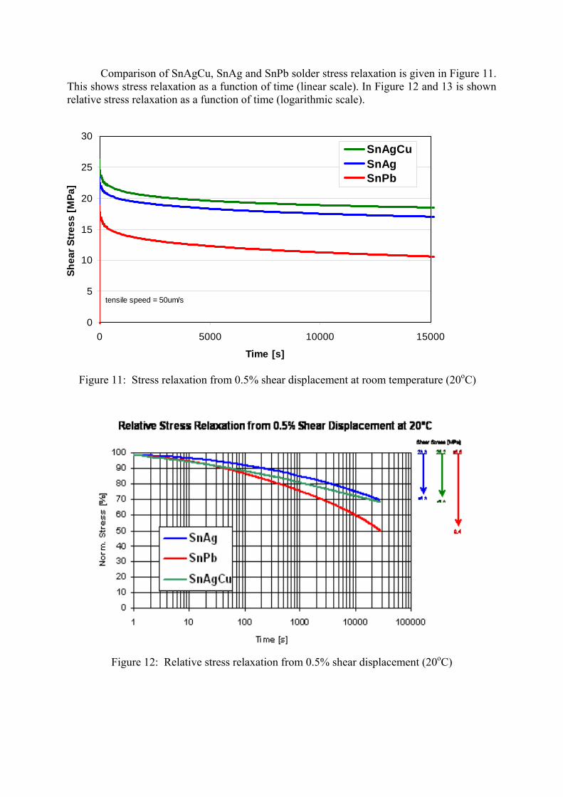
Comparison of SnAgCu, SnAg and SnPb solder stress relaxation is given in Figure 11. This shows stress relaxation as a function of time (linear scale). In Figure 12 and 13 is shown relative stress relaxation as a function of time (logarithmic scale).
0
5
10
15
20
25
30
0 5000 10000 15000
Time [s]
Shea
r Str
ess
[MPa
]
SnAgCuSnAgSnPb
tensile speed = 50um/s
Figure 11: Stress relaxation from 0.5% shear displacement at room temperature (20oC)
Figure 12: Relative stress relaxation from 0.5% shear displacement (20oC)
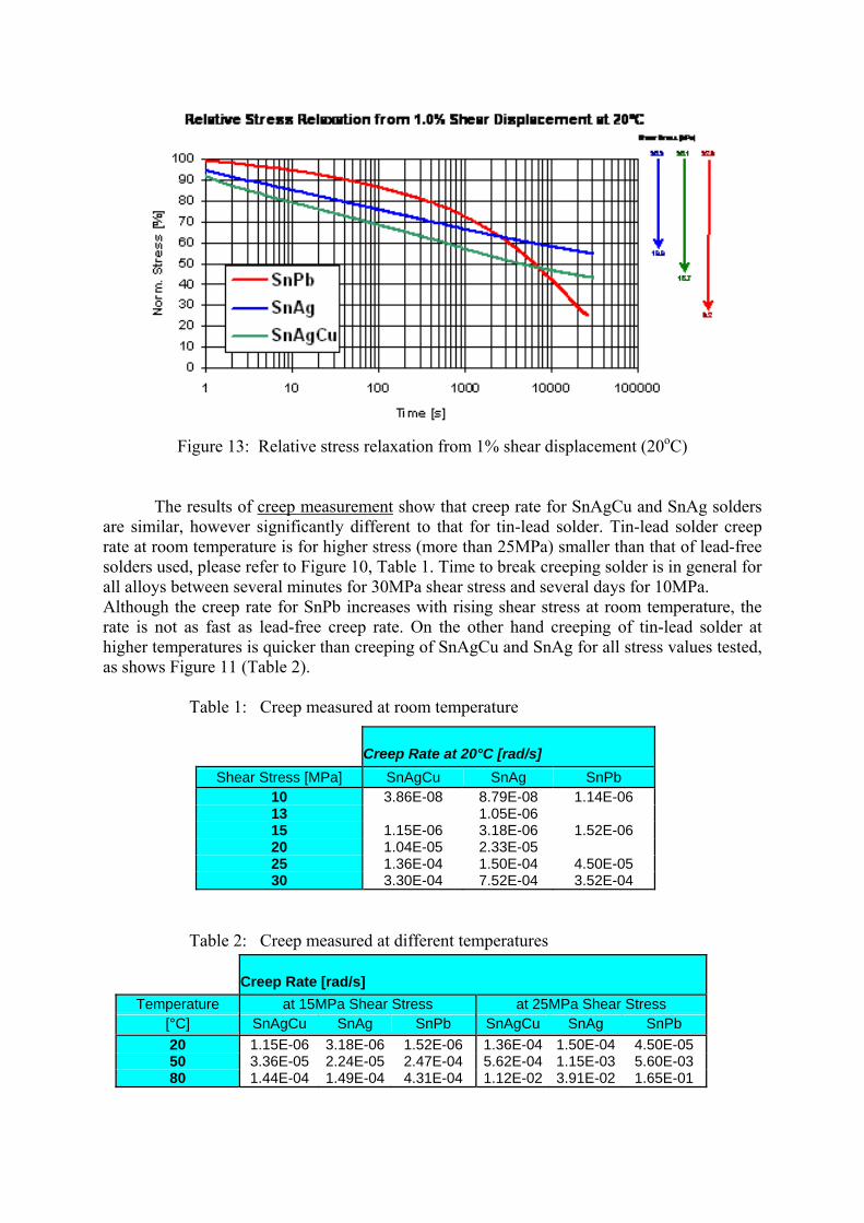
Figure 13: Relative stress relaxation from 1% shear displacement (20oC)
The results of creep measurement show that creep rate for SnAgCu and SnAg solders are similar, however significantly different to that for tin-lead solder. Tin-lead solder creep rate at room temperature is for higher stress (more than 25MPa) smaller than that of lead-free solders used, please refer to Figure 10, Table 1. Time to break creeping solder is in general for all alloys between several minutes for 30MPa shear stress and several days for 10MPa. Although the creep rate for SnPb increases with rising shear stress at room temperature, the rate is not as fast as lead-free creep rate. On the other hand creeping of tin-lead solder at higher temperatures is quicker than creeping of SnAgCu and SnAg for all stress values tested, as shows Figure 11 (Table 2).
Table 1: Creep measured at room temperature
Table 2: Creep measured at different temperatures
Creep Rate at 20°C [rad/s] Shear Stress [MPa] SnAgCu SnAg SnPb
10 3.86E-08 8.79E-08 1.14E-06 13 1.05E-06 15 1.15E-06 3.18E-06 1.52E-06 20 1.04E-05 2.33E-05 25 1.36E-04 1.50E-04 4.50E-05 30 3.30E-04 7.52E-04 3.52E-04
Creep Rate [rad/s] Temperature at 15MPa Shear Stress at 25MPa Shear Stress
[°C] SnAgCu SnAg SnPb SnAgCu SnAg SnPb 20 1.15E-06 3.18E-06 1.52E-06 1.36E-04 1.50E-04 4.50E-05 50 3.36E-05 2.24E-05 2.47E-04 5.62E-04 1.15E-03 5.60E-03 80 1.44E-04 1.49E-04 4.31E-04 1.12E-02 3.91E-02 1.65E-01
Stress relaxation was measured from constant displacement of the solder. This solution was chosen because the thermal stress applied on PCB evokes that all solder joints are not loaded with the same stress but with the same strain. Results of stress relaxation due to 0.5% shear displacement (Fig. 12) show that stress relaxation speeds are similar for all solders that were used in this measurement. To obtain 0.5% of shear displacement was needed to apply much higher stress in case of lead-free solders than in SnPb case. This is a consequence of higher strength of SnAgCu and SnAg solder. In Figure 13 is shown curve of stress relaxation due to 1% of shear displacement of solder joint. One can claim that SnAgCu and SnAg solders relax in first 500 seconds more quickly than standard SnPb solder. After this time the stress value for lead-free solders is converging to its residual point, whereas that for tin-lead solder is still decreasing. As can be seen in Figure 12 and 13 SnAgCu solder has performed even better in strength than SnAg solder.
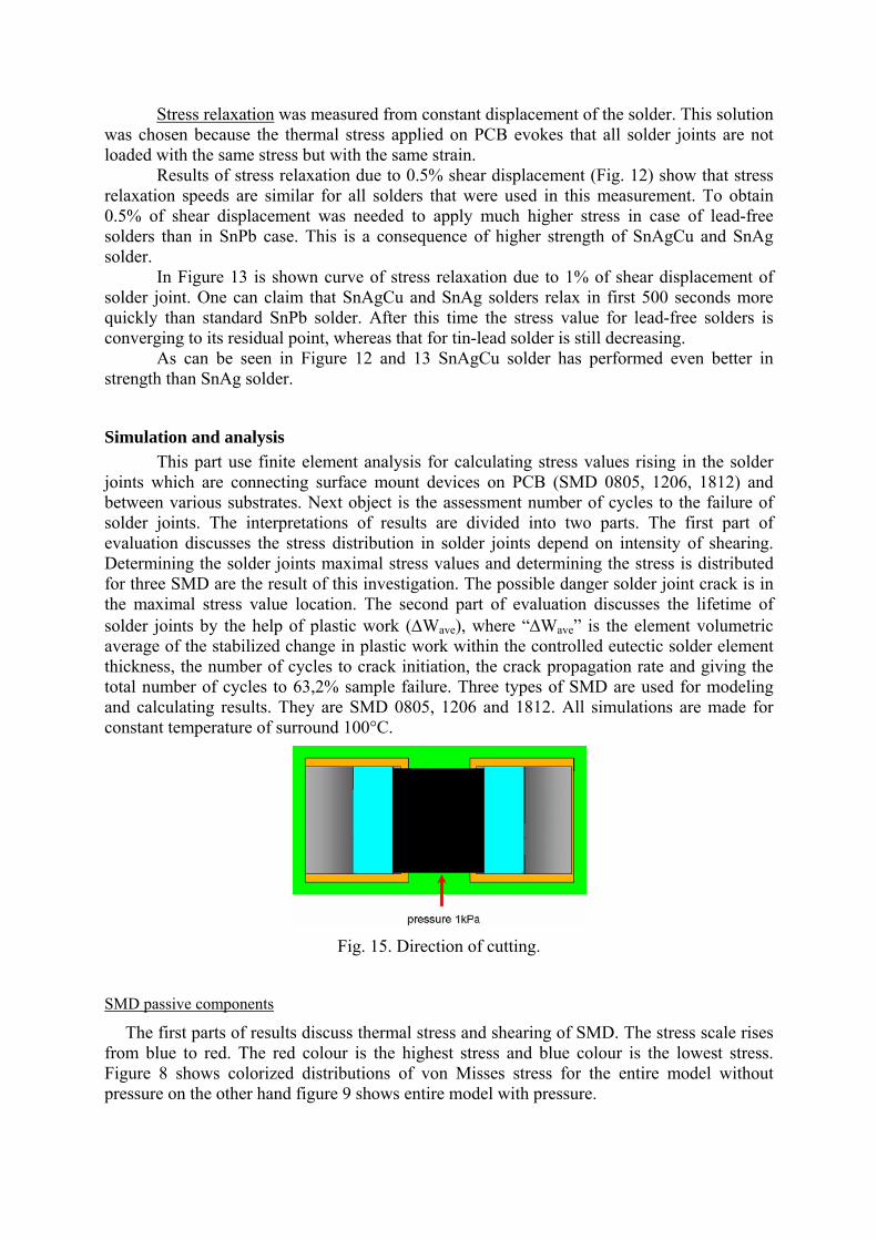
Simulation and analysis This part use finite element analysis for calculating stress values rising in the solder
joints which are connecting surface mount devices on PCB (SMD 0805, 1206, 1812) and between various substrates. Next object is the assessment number of cycles to the failure of solder joints. The interpretations of results are divided into two parts. The first part of evaluation discusses the stress distribution in solder joints depend on intensity of shearing. Determining the solder joints maximal stress values and determining the stress is distributed for three SMD are the result of this investigation. The possible danger solder joint crack is in the maximal stress value location. The second part of evaluation discusses the lifetime of solder joints by the help of plastic work (∆Wave), where “∆Wave” is the element volumetric average of the stabilized change in plastic work within the controlled eutectic solder element thickness, the number of cycles to crack initiation, the crack propagation rate and giving the total number of cycles to 63,2% sample failure. Three types of SMD are used for modeling and calculating results. They are SMD 0805, 1206 and 1812. All simulations are made for constant temperature of surround 100°C.
Fig. 15. Direction of cutting.
SMD passive components
The first parts of results discuss thermal stress and shearing of SMD. The stress scale rises from blue to red. The red colour is the highest stress and blue colour is the lowest stress. Figure 8 shows colorized distributions of von Misses stress for the entire model without pressure on the other hand figure 9 shows entire model with pressure.
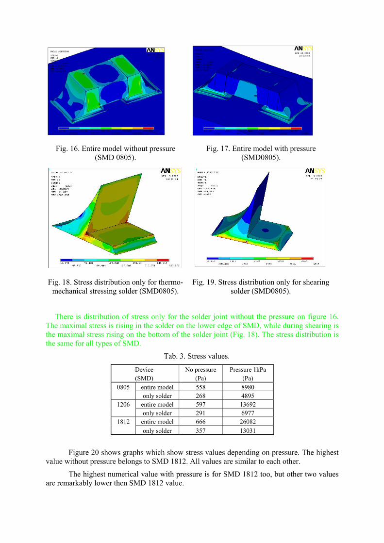
Fig. 16. Entire model without pressure (SMD 0805).
Fig. 17. Entire model with pressure (SMD0805).
Fig. 18. Stress distribution only for thermo-mechanical stressing solder (SMD0805).
Fig. 19. Stress distribution only for shearing solder (SMD0805).
There is distribution of stress only for the solder joint without the pressure on figure 16. The maximal stress is rising in the solder on the lower edge of SMD, while during shearing is the maximal stress rising on the bottom of the solder joint (Fig. 18). The stress distribution is the same for all types of SMD.
Tab. 3. Stress values.
Device No pressure Pressure 1kPa (SMD) (Pa) (Pa)
0805 entire model 558 8980 only solder 268 4895
1206 entire model 597 13692 only solder 291 6977
1812 entire model 666 26082 only solder 357 13031
Figure 20 shows graphs which show stress values depending on pressure. The highest value without pressure belongs to SMD 1812. All values are similar to each other.
The highest numerical value with pressure is for SMD 1812 too, but other two values are remarkably lower then SMD 1812 value.
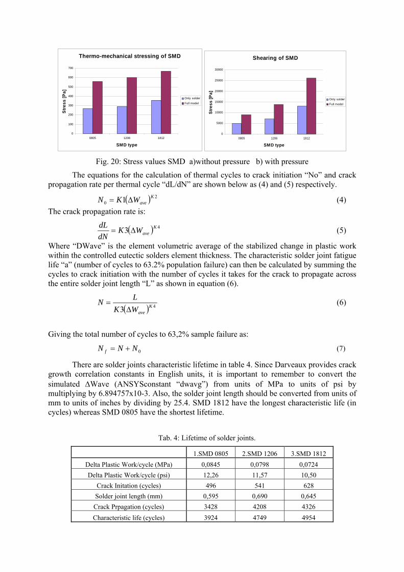
Thermo-mechanical stressing of SMD
0
100
200
300
400
500
600
700
0805 1206 1812
SMD type
Stre
ss [P
a]
Only solderFull model
Shearing of SMD
0
5000
10000
15000
20000
25000
30000
0805 1206 1812
SMD type
Stre
ss [P
a]
Only solderFull model
Fig. 20: Stress values SMD a)without pressure b) with pressure
The equations for the calculation of thermal cycles to crack initiation “No” and crack propagation rate per thermal cycle “dL/dN” are shown below as (4) and (5) respectively.
( ) 20 1 K
aveWKN ∆= (4) The crack propagation rate is:
( ) 43 KaveWK
dNdL
∆= (5)
Where “DWave” is the element volumetric average of the stabilized change in plastic work within the controlled eutectic solders element thickness. The characteristic solder joint fatigue life “a” (number of cycles to 63.2% population failure) can then be calculated by summing the cycles to crack initiation with the number of cycles it takes for the crack to propagate across the entire solder joint length “L” as shown in equation (6).
( ) 43 K
aveWKLN
∆= (6)
Giving the total number of cycles to 63,2% sample failure as:
0NNN f += (7)
There are solder joints characteristic lifetime in table 4. Since Darveaux provides crack growth correlation constants in English units, it is important to remember to convert the simulated ∆Wave (ANSYSconstant “dwavg”) from units of MPa to units of psi by multiplying by 6.894757x10⁻³. Also, the solder joint length should be converted from units of mm to units of inches by dividing by 25.4. SMD 1812 have the longest characteristic life (in cycles) whereas SMD 0805 have the shortest lifetime.
Tab. 4: Lifetime of solder joints.
1.SMD 0805 2.SMD 1206 3.SMD 1812 Delta Plastic Work/cycle (MPa) 0,0845 0,0798 0,0724 Delta Plastic Work/cycle (psi) 12,26 11,57 10,50
Crack Initation (cycles) 496 541 628 Solder joint length (mm) 0,595 0,690 0,645 Crack Prpagation (cycles) 3428 4208 4326 Characteristic life (cycles) 3924 4749 4954
Life time of solder joints
0
1000
2000
3000
4000
5000
6000
1 2 3
SMD
Cyc
les
Crack propagationCharacteristic life
Fig. 21. Life time of solder joints – co jsou jednotlivé sloupce?
In light of reliability of solder joints are SMD 1812 the best. Its lifetime is about 20%
higher then others.
Different substrates connection
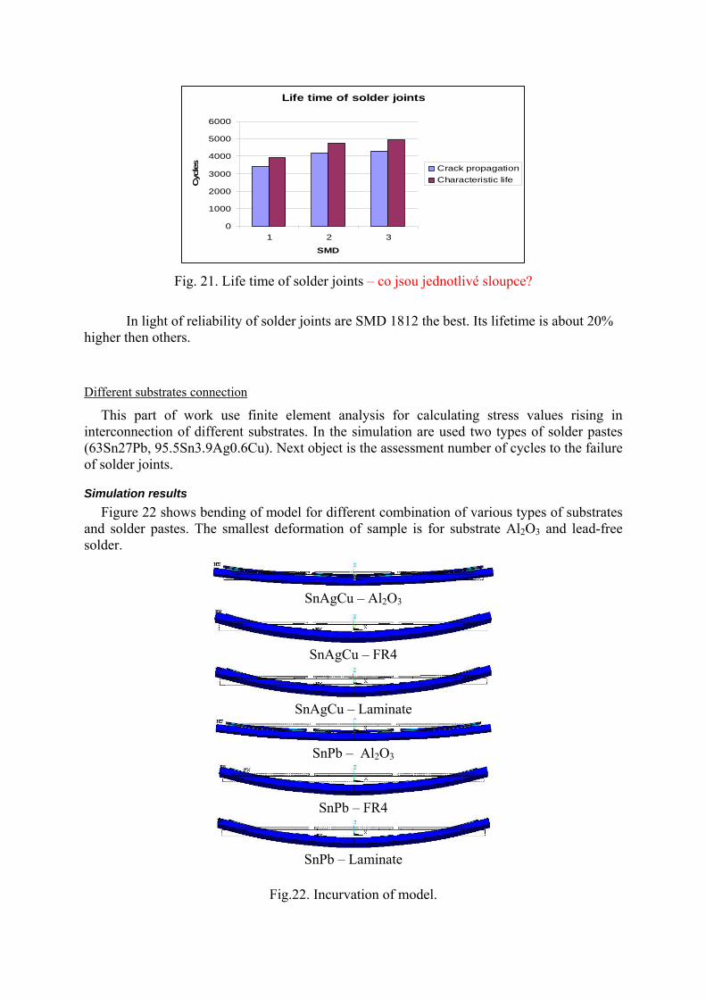
This part of work use finite element analysis for calculating stress values rising in interconnection of different substrates. In the simulation are used two types of solder pastes (63Sn27Pb, 95.5Sn3.9Ag0.6Cu). Next object is the assessment number of cycles to the failure of solder joints.
Simulation results Figure 22 shows bending of model for different combination of various types of substrates
and solder pastes. The smallest deformation of sample is for substrate Al2O3 and lead-free solder.
SnAgCu – Al2O3
SnAgCu – FR4
SnAgCu – Laminate
SnPb – Al2O3
SnPb – FR4
SnPb – Laminate
Fig.22. Incurvation of model.
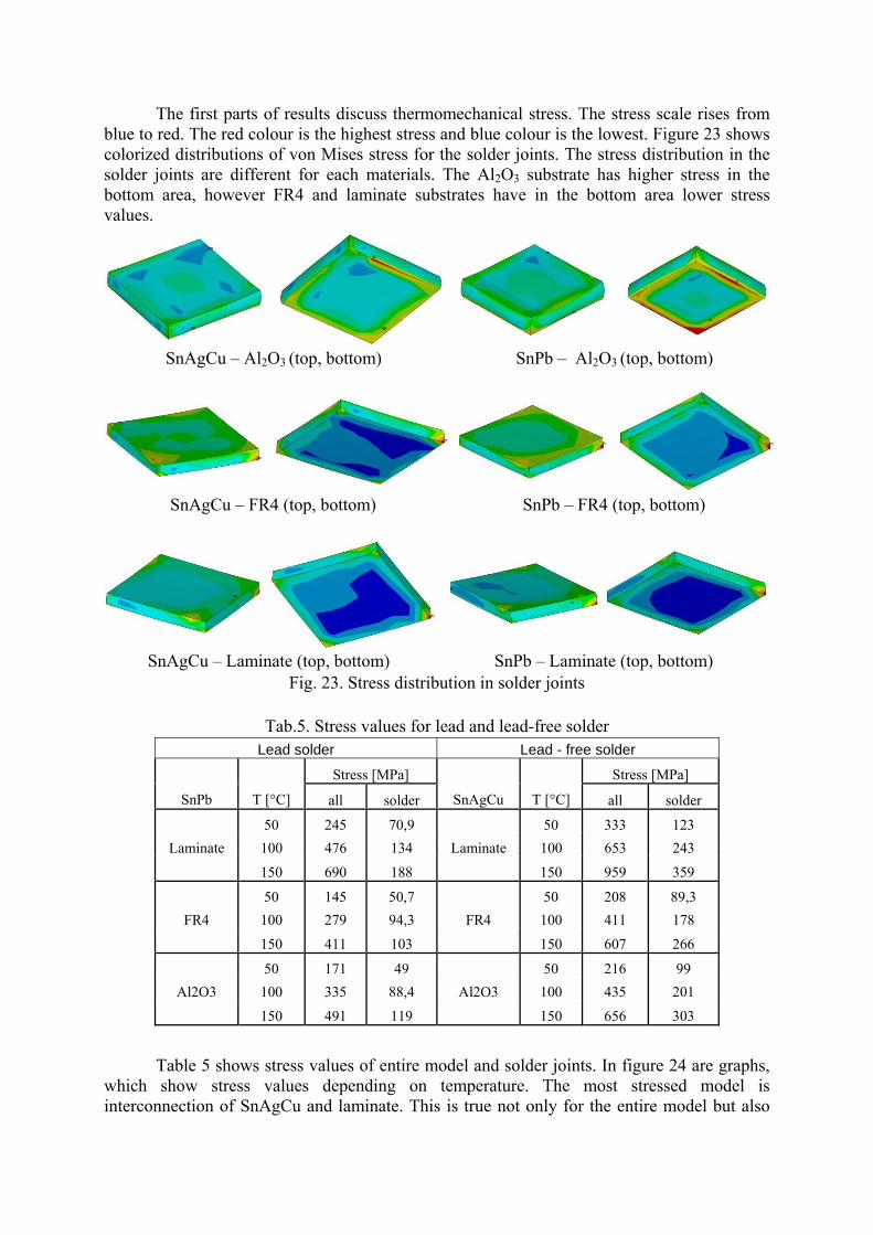
The first parts of results discuss thermomechanical stress. The stress scale rises from blue to red. The red colour is the highest stress and blue colour is the lowest. Figure 23 shows colorized distributions of von Mises stress for the solder joints. The stress distribution in the solder joints are different for each materials. The Al2O3 substrate has higher stress in the bottom area, however FR4 and laminate substrates have in the bottom area lower stress values.
SnAgCu – Al2O3 (top, bottom) SnPb – Al2O3 (top, bottom)
SnAgCu – FR4 (top, bottom) SnPb – FR4 (top, bottom)
SnAgCu – Laminate (top, bottom) SnPb – Laminate (top, bottom) Fig. 23. Stress distribution in solder joints
Tab.5. Stress values for lead and lead-free solder
Lead solder Lead - free solder
Stress [MPa] Stress [MPa]
SnPb T [°C] all solder SnAgCu T [°C] all solder
50 245 70,9 50 333 123 Laminate 100 476 134 Laminate 100 653 243
150 690 188 150 959 359
50 145 50,7 50 208 89,3 FR4 100 279 94,3 FR4 100 411 178
150 411 103 150 607 266
50 171 49 50 216 99 Al2O3 100 335 88,4 Al2O3 100 435 201
150 491 119 150 656 303
Table 5 shows stress values of entire model and solder joints. In figure 24 are graphs, which show stress values depending on temperature. The most stressed model is interconnection of SnAgCu and laminate. This is true not only for the entire model but also
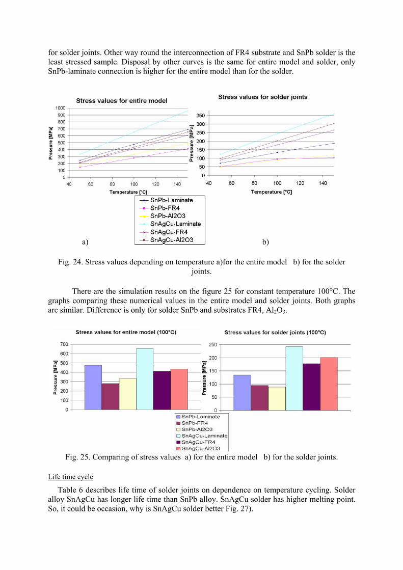
for solder joints. Other way round the interconnection of FR4 substrate and SnPb solder is the least stressed sample. Disposal by other curves is the same for entire model and solder, only SnPb-laminate connection is higher for the entire model than for the solder.
a) b)
Fig. 24. Stress values depending on temperature a)for the entire model b) for the solder joints.
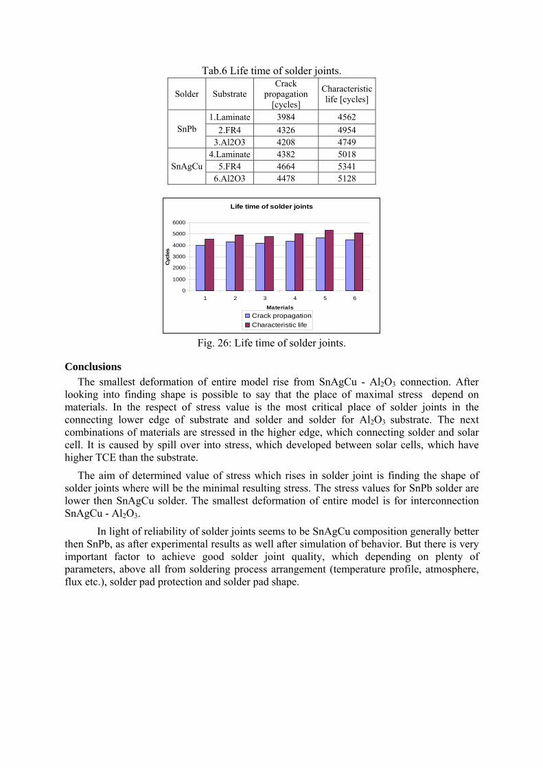
There are the simulation results on the figure 25 for constant temperature 100°C. The
graphs comparing these numerical values in the entire model and solder joints. Both graphs are similar. Difference is only for solder SnPb and substrates FR4, Al2O3.
Fig. 25. Comparing of stress values a) for the entire model b) for the solder joints.
Life time cycle
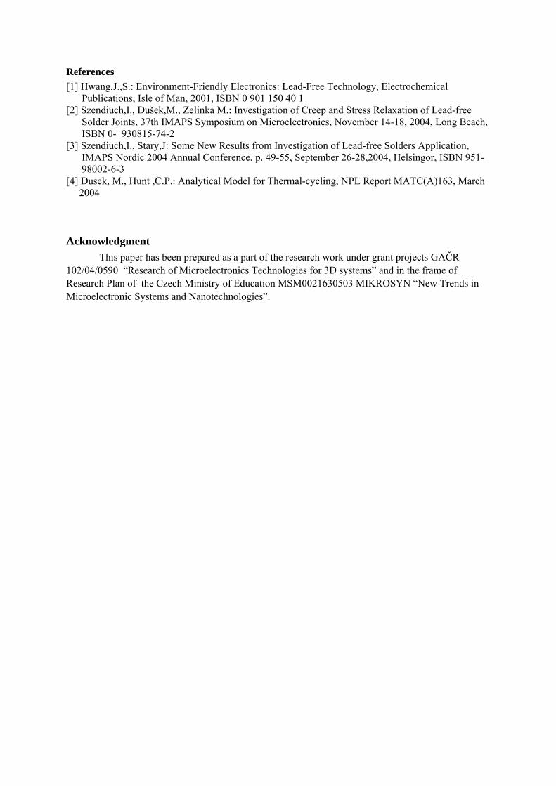
Table 6 describes life time of solder joints on dependence on temperature cycling. Solder alloy SnAgCu has longer life time than SnPb alloy. SnAgCu solder has higher melting point. So, it could be occasion, why is SnAgCu solder better Fig. 27).
Tab.6 Life time of solder joints.
Solder Substrate Crack
propagation [cycles]
Characteristic life [cycles]
1.Laminate 3984 4562 2.FR4 4326 4954 SnPb
3.Al2O3 4208 4749 4.Laminate 4382 5018
5.FR4 4664 5341 SnAgCu 6.Al2O3 4478 5128
Life time of solder joints
0
1000
2000
3000
4000
5000
6000
1 2 3 4 5 6
Materials
Cyc
les
Crack propagationCharacteristic life
Fig. 26: Life time of solder joints.
Conclusions The smallest deformation of entire model rise from SnAgCu - Al2O3 connection. After
looking into finding shape is possible to say that the place of maximal stress depend on materials. In the respect of stress value is the most critical place of solder joints in the connecting lower edge of substrate and solder and solder for Al2O3 substrate. The next combinations of materials are stressed in the higher edge, which connecting solder and solar cell. It is caused by spill over into stress, which developed between solar cells, which have higher TCE than the substrate.
The aim of determined value of stress which rises in solder joint is finding the shape of solder joints where will be the minimal resulting stress. The stress values for SnPb solder are lower then SnAgCu solder. The smallest deformation of entire model is for interconnection SnAgCu - Al2O3.
In light of reliability of solder joints seems to be SnAgCu composition generally better then SnPb, as after experimental results as well after simulation of behavior. But there is very important factor to achieve good solder joint quality, which depending on plenty of parameters, above all from soldering process arrangement (temperature profile, atmosphere, flux etc.), solder pad protection and solder pad shape.
References [1] Hwang,J.,S.: Environment-Friendly Electronics: Lead-Free Technology, Electrochemical Publications, Isle of Man, 2001, ISBN 0 901 150 40 1 [2] Szendiuch,I., Dušek,M., Zelinka M.: Investigation of Creep and Stress Relaxation of Lead-free Solder Joints, 37th IMAPS Symposium on Microelectronics, November 14-18, 2004, Long Beach, ISBN 0- 930815-74-2 [3] Szendiuch,I., Stary,J: Some New Results from Investigation of Lead-free Solders Application, IMAPS Nordic 2004 Annual Conference, p. 49-55, September 26-28,2004, Helsingor, ISBN 951- 98002-6-3 [4] Dusek, M., Hunt ,C.P.: Analytical Model for Thermal-cycling, NPL Report MATC(A)163, March 2004
Acknowledgment This paper has been prepared as a part of the research work under grant projects GAČR 102/04/0590 “Research of Microelectronics Technologies for 3D systems” and in the frame of Research Plan of the Czech Ministry of Education MSM0021630503 MIKROSYN “New Trends in Microelectronic Systems and Nanotechnologies”.