Embed Size (px)
Citation preview
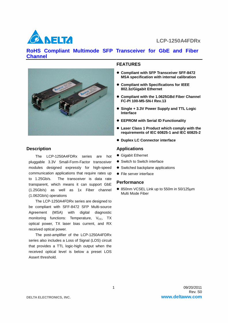
LCP-1250A4FDRx
DELTA ELECTRONICS, INC.
1 09/20/2011 Rev. S0
www.deltaww.com
RoHS Compliant Multimode SFP Transceiver for GbE and Fiber Channel
FEATURES
Compliant with SFP Transceiver SFF-8472 MSA specification with internal calibration
Compliant with Specifications for IEEE 802.3z/Gigabit Ethernet
Compliant with the 1.0625GBd Fiber Channel FC-PI 100-M5-SN-I Rev.13
Single + 3.3V Power Supply and TTL Logic Interface
EEPROM with Serial ID Functionality
Laser Class 1 Product which comply with the requirements of IEC 60825-1 and IEC 60825-2
Duplex LC Connector interface
Description
The LCP-1250A4FDRx series are hot
pluggable 3.3V Small-Form-Factor transceiver
modules designed expressly for high-speed
communication applications that require rates up
to 1.25Gb/s. The transceiver is data rate
transparent, which means it can support GbE
(1.25Gb/s) as well as 1x Fiber channel
(1.062Gb/s) operations
The LCP-1250A4FDRx series are designed to
be compliant with SFF-8472 SFP Multi-source
Agreement (MSA) with digital diagnostic
monitoring functions: Temperature, VCC, TX
optical power, TX laser bias current, and RX
received optical power.
The post-amplifier of the LCP-1250A4FDRx
series also includes a Loss of Signal (LOS) circuit
that provides a TTL logic-high output when the
received optical level is below a preset LOS
Assert threshold.
Applications Gigabit Ethernet
Switch to Switch interface
Switched backplane applications
File server interface
Performance 850nm VCSEL Link up to 550m in 50/125µm
Multi Mode Fiber
LCP-1250A4FDRx
DELTA ELECTRONICS, INC.
2 09/20/2011 Rev. S0
www.deltaww.com
Absolute Maximum Ratings
Parameter Symbol Min. Typ. Max. Unit Note Storage Temperature Ts -40 85 ºC Supply Voltage VCC 0 5 V
Recommended Operating Conditions
Parameter Symbol Min. Typ. Max. Unit Note Case Operating Temperature TC -5 70 ºC 1 Supply Voltage VCC 3.135 3.465 V
Note 1: See order information
Electrical Characteristics
(VCC=3.3V ± 5%)
Parameter Symbol Min. Typ. Max. Unit Note Total Supply Current ICCT 180 300 mA
Transmitter Transmitter Differential Input Voltage VDT 0.5 2.4 V 1 Transmitter Disable Input-High VDISH 2 VCC+0.3 V Transmitter Disable Input-Low VDISL 0 0.8 V Transmitter Fault Pull up Resistor RTX_FAULT 4.7 10 kΩ 2 Transmitter Fault Output-High VTXFH 2 VCC+0.3 V 2 Transmitter Fault Output-Low VTXFL 0 0.8 V 2
Receiver Receiver Differential Output Voltage VDR 0.35 1 2 V 3 Receiver LOS Load RRXLOS 4.7 10 kΩ 2 LOS Output Voltage-High VLOSH 2 VCC+0.3 V 2 LOS Output Voltage-Low VLOSL 0 0.8 V 2 Output Data Rise/Fall Time tr / tf 220 psec 4
Notes:
1. Internally AC coupled and terminated to 100Ohm differential load.
2. Pull up to VCC on host Board
3. Internally AC coupled, but requires a 100Ohm differential termination at or internal to Serializer/
Deserializer.
4. These are 20%~80% values
LCP-1250A4FDRx
DELTA ELECTRONICS, INC.
3 09/20/2011 Rev. S0
www.deltaww.com
Optical Characteristics (VCC=3.3V ± 5%, Data Rate=1250Mb/sec, PRBS=27-1 NRZ)
Parameter Symbol Min. Typ. Max. Unit Note Transmitter
Output Optical Power (Avg.) PO -9.5 -4 dBm Optical Extinction Ratio ER 9 dB Center Wavelength λC 830 850 860 nm Spectral Width (RMS) σ 0.85 nm Optical Rise/ Fall Time tr/tf 260 pec 1
Receiver Sensitivity (Avg.) PIN -17 dBm 2 Input Optical Wavelength λ 850 nm LOS-Deasserted (Avg.) PA -17 dBm LOS-Asserted (Avg.) PD -30 dBm LOS-Hysteresis PA-PD 0.5 dB Overload PO -3 dBm
Notes:
1. These are unfiltered 20%~80% values
2. The sensitivity is provided at a BER of 1×10-12or better with an input signal consisting of 1250Mb/s,
27-1 PRBS and ER=9dB.
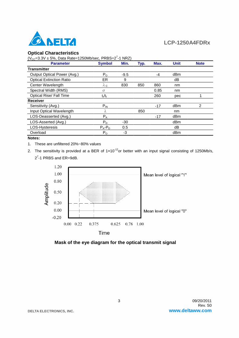
Mask of the eye diagram for the optical transmit signal
LCP-1250A4FDRx
DELTA ELECTRONICS, INC.
4 09/20/2011 Rev. S0
www.deltaww.com
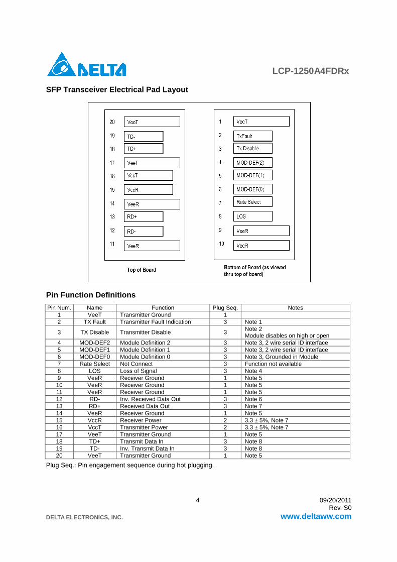
SFP Transceiver Electrical Pad Layout
Pin Function Definitions
Pin Num. Name Function Plug Seq. Notes 1 VeeT Transmitter Ground 1 2 TX Fault Transmitter Fault Indication 3 Note 1
3 TX Disable Transmitter Disable 3 Note 2 Module disables on high or open
4 MOD-DEF2 Module Definition 2 3 Note 3, 2 wire serial ID interface 5 MOD-DEF1 Module Definition 1 3 Note 3, 2 wire serial ID interface 6 MOD-DEF0 Module Definition 0 3 Note 3, Grounded in Module 7 Rate Select Not Connect 3 Function not available 8 LOS Loss of Signal 3 Note 4 9 VeeR Receiver Ground 1 Note 5 10 VeeR Receiver Ground 1 Note 5 11 VeeR Receiver Ground 1 Note 5 12 RD- Inv. Received Data Out 3 Note 6 13 RD+ Received Data Out 3 Note 7 14 VeeR Receiver Ground 1 Note 5 15 VccR Receiver Power 2 3.3 ± 5%, Note 7 16 VccT Transmitter Power 2 3.3 ± 5%, Note 7 17 VeeT Transmitter Ground 1 Note 5 18 TD+ Transmit Data In 3 Note 8 19 TD- Inv. Transmit Data In 3 Note 8 20 VeeT Transmitter Ground 1 Note 5
Plug Seq.: Pin engagement sequence during hot plugging.
LCP-1250A4FDRx
DELTA ELECTRONICS, INC.
5 09/20/2011 Rev. S0
www.deltaww.com
Notes:
1) TX Fault is an open collector/drain output, which should be pulled up with a 4.7K – 10KΩ resistor on the host
board. Pull up voltage between 2.0V and VccT, R+0.3V. When high, output indicates a laser fault of some kind.
Low indicates normal operation. In the low state, the output will be pulled to < 0.8V.
2) TX disable is an input that is used to shut down the transmitter optical output. It is pulled up within the module
with a 4.7 – 10 K Ω resistor. Its states are:
Low (0 – 0.8V): Transmitter on
(>0.8, < 2.0V): Undefined
High (2.0 – 3.465V): Transmitter Disabled
Open: Transmitter Disabled
3) Mod-Def 0,1,2. These are the module definition pins. They should be pulled up with a 4.7K – 10KΩresistor on the
host board. The pull-up voltage shall be VccT or VccR (see Section IV for further details). Mod-Def 0 is grounded
by the module to indicate that the module is present Mod-Def 1 is the clock line of two wire serial interface for
serial ID Mod-Def 2 is the data line of two wire serial interface for serial ID
4) LOS (Loss of Signal) is an open collector/drain output, which should be pulled up with a 4.7K – 10KΩ resistor.
Pull up voltage between 2.0V and VccT, R+0.3V. When high, this output indicates the received optical power is
below the worst-case receiver sensitivity (as defined by the standard in use). Low indicates normal operation. In
the low state, the output will be pulled to < 0.8V.
5) VeeR and VeeT may be internally connected within the SFP module.
6) RD-/+: These are the differential receiver outputs. They are AC coupled 100Ω differential lines which should be
terminated with 100Ω (differential) at the user SERDES. The AC coupling is done inside the module and is thus
not required on the host board. The voltage swing on these lines will be between 370 and 2000 mV differential
(185 – 1000 mV single ended) when properly terminated.
7) VccR and VccT are the receiver and transmitter power supplies. They are defined as 3.3V ±5% at the SFP
connector pin. Maximum supply current is 300mA. Recommended host board power supply filtering is shown
below. Inductors with DC resistance of less than 1 ohm should be used in order to maintain the required voltage
at the SFP input pin with 3.3V supply voltage. When the recommended supply-filtering network is used, hot
plugging of the SFP transceiver module will result in an inrush current of no more than 30mA greater than the
steady state value. VccR and VccT may be internally connected within the SFP transceiver module.
8) TD-/+: These are the differential transmitter inputs. They are AC-coupled, differential lines with 100Ω
differential termination inside the module. The AC coupling is done inside the module and is thus not
required on the host board. The inputs will accept differential swings of 500 – 2400 mV (250 – 1200
mV single-ended), though it is recommended that values between 500 and 1200 mV differential (250 –
600 mV single-ended) be used for best EMI performance.
LCP-1250A4FDRx
DELTA ELECTRONICS, INC.
6 09/20/2011 Rev. S0
www.deltaww.com
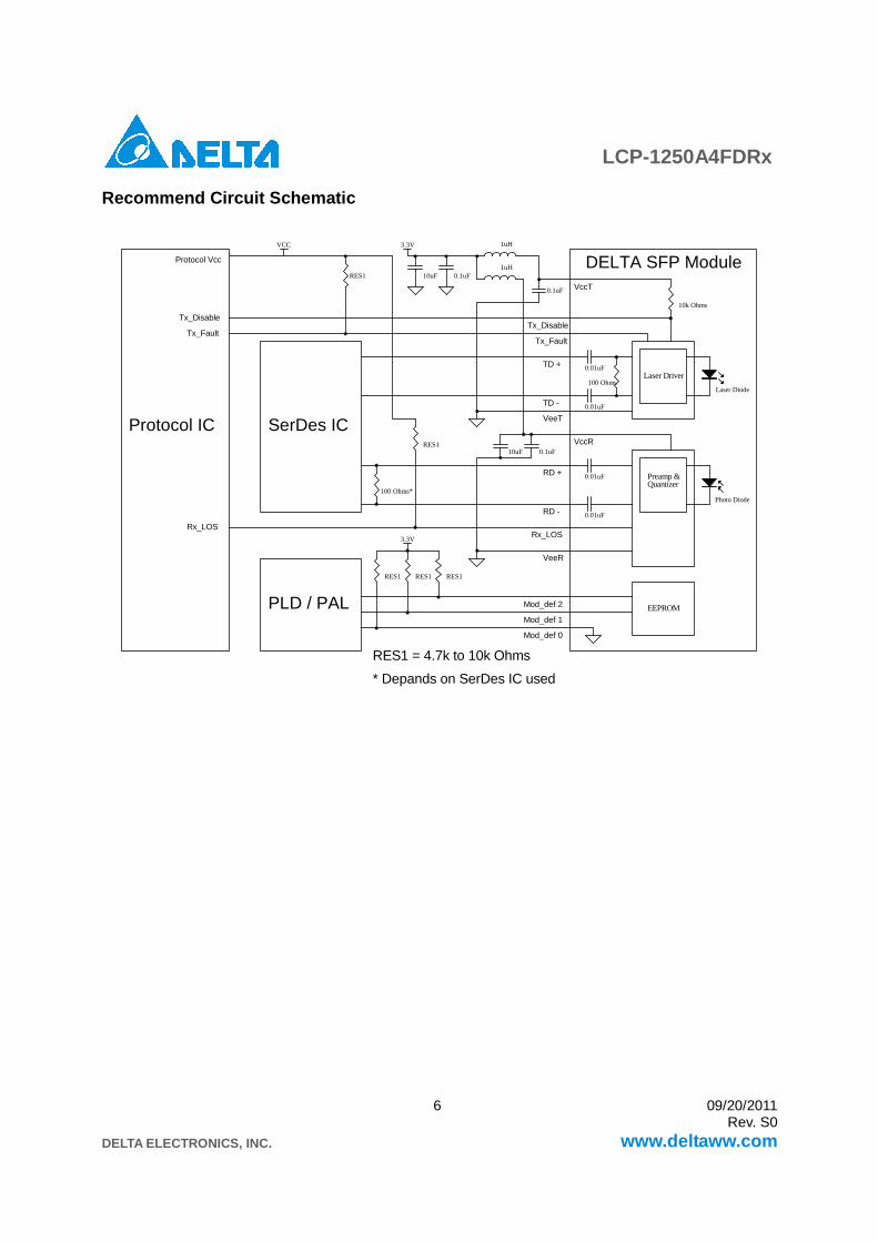
Recommend Circuit Schematic
Laser Diode
Photo Diode
1uH
1uH0.1uF10uF
0.1uF
0.01uF
0.01uF
0.01uF
0.01uF
0.1uF10uF
RES1
RES1
100 Ohms*
RES1 RES1 RES1
10k Ohms
100 Ohms
VCC
Protocol Vcc
SerDes ICProtocol IC
PLD / PAL Mod_def 2
Mod_def 1
Mod_def 0
3.3V
3.3V
DELTA SFP Module
Preamp &
Tx_Disable
Quantizer
Tx_Fault
TD +
TD -
VeeT
RD +
RD -
Rx_LOS
VeeR
Tx_Disable
Tx_Fault
Rx_LOS
RES1 = 4.7k to 10k Ohms
VccT
VccR
Laser Driver
* Depands on SerDes IC used
EEPROM
LCP-1250A4FDRx
DELTA ELECTRONICS, INC.
7 09/20/2011 Rev. S0
www.deltaww.com
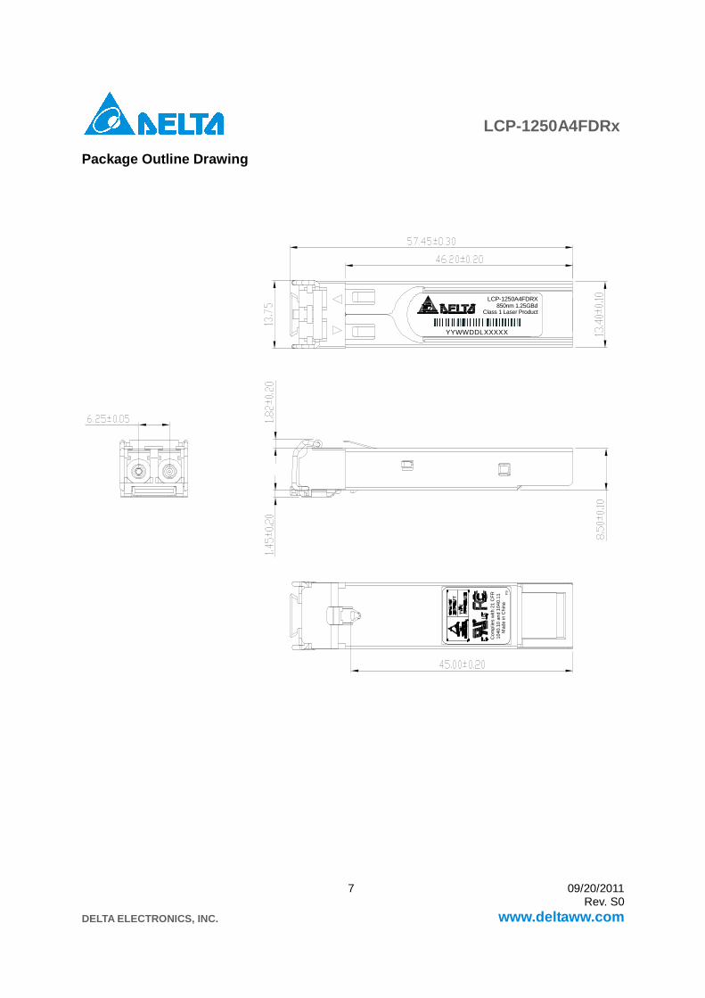
Package Outline Drawing
Com
plie
s w
ith 2
1 C
FR
1040
.10
and
1040
.11
Mad
e in
Chi
naF
S
LCP-1250A4FDRX850nm 1.25GBd
Class 1 Laser Product
YYWWDDLXXXXX
LCP-1250A4FDRx
DELTA ELECTRONICS, INC.
8 09/20/2011 Rev. S0
www.deltaww.com
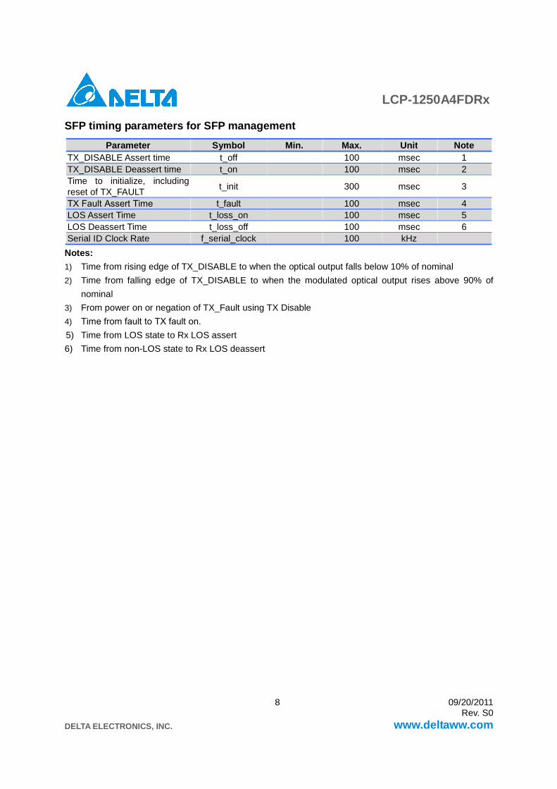
SFP timing parameters for SFP management
Parameter Symbol Min. Max. Unit Note TX_DISABLE Assert time t_off 100 msec 1 TX_DISABLE Deassert time t_on 100 msec 2 Time to initialize, including reset of TX_FAULT
t_init 300 msec 3
TX Fault Assert Time t_fault 100 msec 4 LOS Assert Time t_loss_on 100 msec 5 LOS Deassert Time t_loss_off 100 msec 6 Serial ID Clock Rate f_serial_clock 100 kHz
Notes:
1) Time from rising edge of TX_DISABLE to when the optical output falls below 10% of nominal
2) Time from falling edge of TX_DISABLE to when the modulated optical output rises above 90% of
nominal
3) From power on or negation of TX_Fault using TX Disable
4) Time from fault to TX fault on. 5) Time from LOS state to Rx LOS assert
6) Time from non-LOS state to Rx LOS deassert
LCP-1250A4FDRx
DELTA ELECTRONICS, INC.
9 09/20/2011 Rev. S0
www.deltaww.com
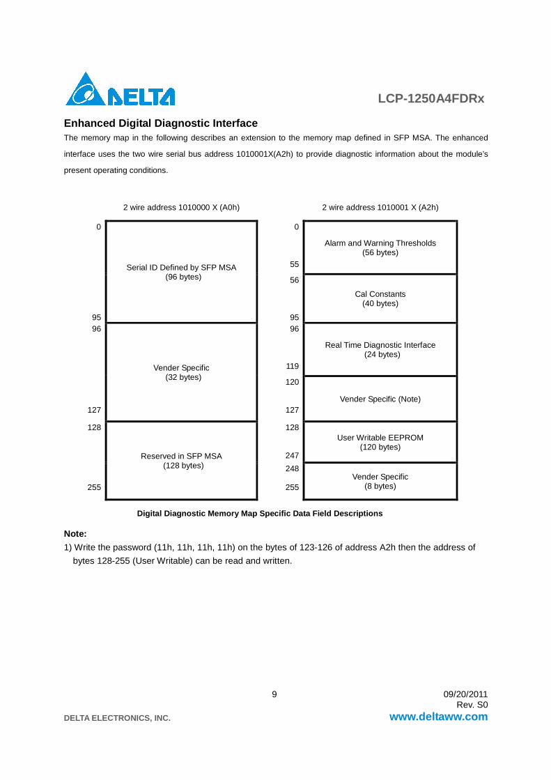
Enhanced Digital Diagnostic Interface
The memory map in the following describes an extension to the memory map defined in SFP MSA. The enhanced
interface uses the two wire serial bus address 1010001X(A2h) to provide diagnostic information about the module’s
present operating conditions.
2 wire address 1010000 X (A0h) 2 wire address 1010001 X (A2h)
0
Serial ID Defined by SFP MSA (96 bytes)
0
55
Alarm and Warning Thresholds (56 bytes)
95
56
95
Cal Constants (40 bytes)
96
Vender Specific (32 bytes)
96
119
Real Time Diagnostic Interface (24 bytes)
127
120
127 Vender Specific (Note)
128
Reserved in SFP MSA (128 bytes)
128
247
User Writable EEPROM (120 bytes)
255
248
255 Vender Specific
(8 bytes)
Digital Diagnostic Memory Map Specific Data Field Descriptions
Note:
1) Write the password (11h, 11h, 11h, 11h) on the bytes of 123-126 of address A2h then the address of
bytes 128-255 (User Writable) can be read and written.
LCP-1250A4FDRx
DELTA ELECTRONICS, INC.
10 09/20/2011 Rev. S0
www.deltaww.com
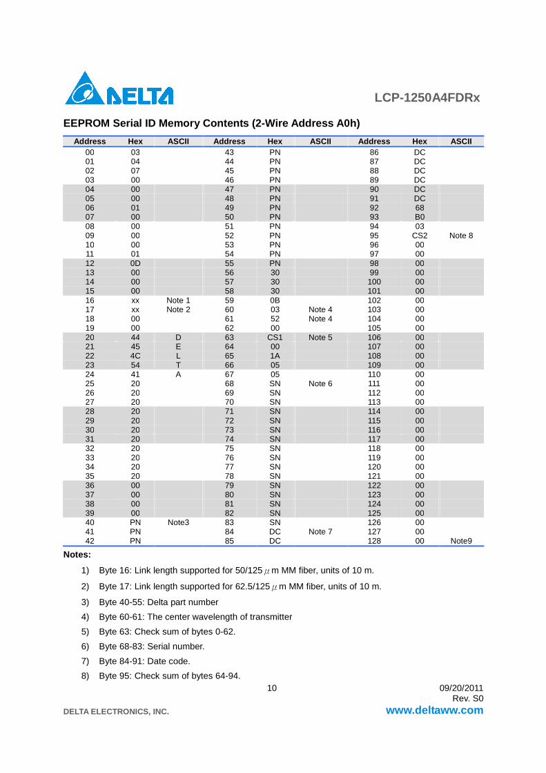
EEPROM Serial ID Memory Contents (2-Wire Address A0h)
Address Hex ASCII Address Hex ASCII Address Hex ASCII 00 03 43 PN 86 DC 01 04 44 PN 87 DC 02 07 45 PN 88 DC 03 00 46 PN 89 DC 04 00 47 PN 90 DC 05 00 48 PN 91 DC 06 01 49 PN 92 68 07 00 50 PN 93 B0 08 00 51 PN 94 03 09 00 52 PN 95 CS2 Note 8 10 00 53 PN 96 00 11 01 54 PN 97 00 12 0D 55 PN 98 00 13 00 56 30 99 00 14 00 57 30 100 00 15 00 58 30 101 00 16 xx Note 1 59 0B 102 00 17 xx Note 2 60 03 Note 4 103 00 18 00 61 52 Note 4 104 00 19 00 62 00 105 00 20 44 D 63 CS1 Note 5 106 00 21 45 E 64 00 107 00 22 4C L 65 1A 108 00 23 54 T 66 05 109 00 24 41 A 67 05 110 00 25 20 68 SN Note 6 111 00 26 20 69 SN 112 00 27 20 70 SN 113 00 28 20 71 SN 114 00 29 20 72 SN 115 00 30 20 73 SN 116 00 31 20 74 SN 117 00 32 20 75 SN 118 00 33 20 76 SN 119 00 34 20 77 SN 120 00 35 20 78 SN 121 00 36 00 79 SN 122 00 37 00 80 SN 123 00 38 00 81 SN 124 00 39 00 82 SN 125 00 40 PN Note3 83 SN 126 00 41 PN 84 DC Note 7 127 00 42 PN 85 DC 128 00 Note9
Notes:
1) Byte 16: Link length supported for 50/125μm MM fiber, units of 10 m.
2) Byte 17: Link length supported for 62.5/125μm MM fiber, units of 10 m.
3) Byte 40-55: Delta part number
4) Byte 60-61: The center wavelength of transmitter
5) Byte 63: Check sum of bytes 0-62.
6) Byte 68-83: Serial number.
7) Byte 84-91: Date code.
8) Byte 95: Check sum of bytes 64-94.
LCP-1250A4FDRx
DELTA ELECTRONICS, INC.
11 09/20/2011 Rev. S0
www.deltaww.com
9) Byte 128 to 255 had been set hex 00.
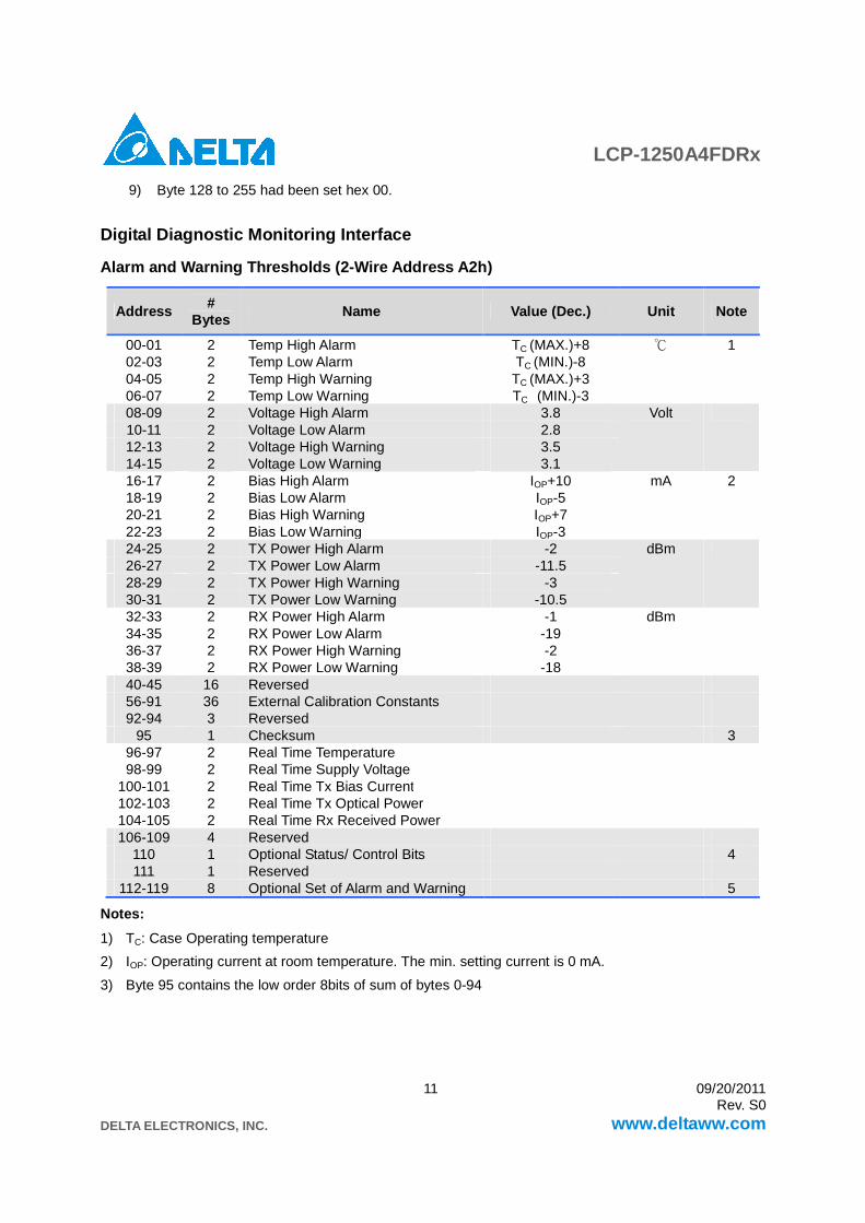
Digital Diagnostic Monitoring Interface
Alarm and Warning Thresholds (2-Wire Address A2h)
Address # Bytes
Name Value (Dec.) Unit Note
00-01 2 Temp High Alarm TC (MAX.)+8 1 02-03 2 Temp Low Alarm TC (MIN.)-8 04-05 2 Temp High Warning TC (MAX.)+3 06-07 2 Temp Low Warning TC (MIN.)-3 08-09 2 Voltage High Alarm 3.8 Volt 10-11 2 Voltage Low Alarm 2.8 12-13 2 Voltage High Warning 3.5 14-15 2 Voltage Low Warning 3.1 16-17 2 Bias High Alarm IOP+10 mA 2 18-19 2 Bias Low Alarm IOP-5 20-21 2 Bias High Warning IOP+7 22-23 2 Bias Low Warning IOP-3 24-25 2 TX Power High Alarm -2 dBm 26-27 2 TX Power Low Alarm -11.5 28-29 2 TX Power High Warning -3 30-31 2 TX Power Low Warning -10.5 32-33 2 RX Power High Alarm -1 dBm 34-35 2 RX Power Low Alarm -19 36-37 2 RX Power High Warning -2 38-39 2 RX Power Low Warning -18 40-45 16 Reversed 56-91 36 External Calibration Constants 92-94 3 Reversed
95 1 Checksum 3 96-97 2 Real Time Temperature 98-99 2 Real Time Supply Voltage
100-101 2 Real Time Tx Bias Current 102-103 2 Real Time Tx Optical Power 104-105 2 Real Time Rx Received Power 106-109 4 Reserved
110 1 Optional Status/ Control Bits 4 111 1 Reserved
112-119 8 Optional Set of Alarm and Warning 5
Notes:
1) TC: Case Operating temperature
2) IOP: Operating current at room temperature. The min. setting current is 0 mA.
3) Byte 95 contains the low order 8bits of sum of bytes 0-94
LCP-1250A4FDRx
DELTA ELECTRONICS, INC.
12 09/20/2011 Rev. S0
www.deltaww.com
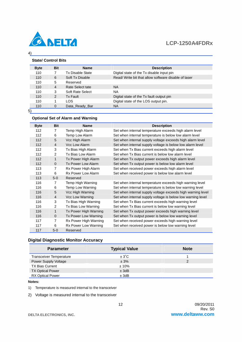
4)
State/ Control Bits
Byte Bit Name Description 110 7 Tx Disable State Digital state of the Tx disable input pin 110 6 Soft Tx Disable Read/ Write bit that allow software disable of laser 110 5 Reserved 110 4 Rate Select tate NA 110 3 Soft Rate Select NA 110 2 Tx Fault Digital state of the Tx fault output pin 110 1 LOS Digital state of the LOS output pin. 110 0 Data_Ready_Bar NA
5)
Optional Set of Alarm and Warning
Byte Bit Name Description 112 7 Temp High Alarm Set when internal temperature exceeds high alarm level 112 6 Temp Low Alarm Set when internal temperature is below low alarm level 112 5 Vcc High Alarm Set when internal supply voltage exceeds high alarm level 112 4 Vcc Low Alarm Set when internal supply voltage is below low alarm level 112 3 Tx Bias High Alarm Set when Tx Bias current exceeds high alarm level 112 2 Tx Bias Low Alarm Set when Tx Bias current is below low alarm level 112 1 Tx Power High Alarm Set when Tx output power exceeds high alarm level 112 0 Tx Power Low Alarm Set when Tx output power is below low alarm level 113 7 Rx Power High Alarm Set when received power exceeds high alarm level 113 6 Rx Power Low Alarm Set when received power is below low alarm level 113 5-0 Reserved 116 7 Temp High Warning Set when internal temperature exceeds high warning level 116 6 Temp Low Warning Set when internal temperature is below low warning level 116 5 Vcc High Warning Set when internal supply voltage exceeds high warning level 116 4 Vcc Low Warning Set when internal supply voltage is below low warning level 116 3 Tx Bias High Warning Set when Tx Bias current exceeds high warning level 116 2 Tx Bias Low Warning Set when Tx Bias current is below low warning level 116 1 Tx Power High Warning Set when Tx output power exceeds high warning level 116 0 Tx Power Low Warning Set when Tx output power is below low warning level 117 7 Rx Power High Warning Set when received power exceeds high warning level 117 6 Rx Power Low Warning Set when received power is below low warning level 117 5-0 Reserved
Digital Diagnostic Monitor Accuracy
Parameter Typical Value Note
Transceiver Temperature ± 3˚C 1 Power Supply Voltage ± 3% 2 TX Bias Current ± 10% TX Optical Power ± 3dB RX Optical Power ± 3dB
Notes:
1) Temperature is measured internal to the transceiver
2) Voltage is measured internal to the transceiver
LCP-1250A4FDRx
DELTA ELECTRONICS, INC.
13 09/20/2011 Rev. S0
www.deltaww.com
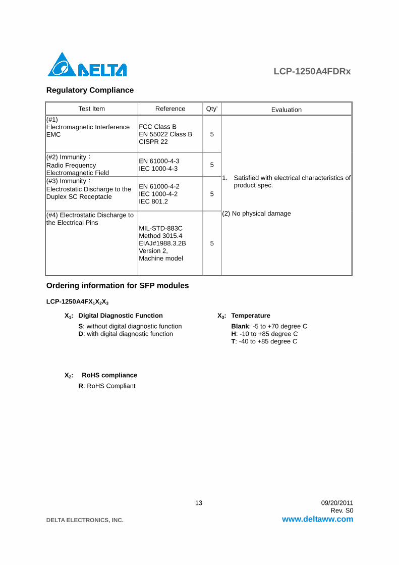
Regulatory Compliance
Test Item Reference Qty’ Evaluation
(#1) Electromagnetic Interference EMC
FCC Class B EN 55022 Class B CISPR 22
5
1. Satisfied with electrical characteristics of product spec.
(2) No physical damage
(#2) Immunity: Radio Frequency Electromagnetic Field
EN 61000-4-3 IEC 1000-4-3
5
(#3) Immunity: Electrostatic Discharge to the Duplex SC Receptacle
EN 61000-4-2 IEC 1000-4-2 IEC 801.2
5
(#4) Electrostatic Discharge to the Electrical Pins
MIL-STD-883C Method 3015.4 EIAJ#1988.3.2B Version 2, Machine model
5
Ordering information for SFP modules
LCP-1250A4FX1X2X3
X1: Digital Diagnostic Function
S: without digital diagnostic function D: with digital diagnostic function
X3: Temperature
Blank: -5 to +70 degree C H: -10 to +85 degree C T: -40 to +85 degree C
X2: RoHS compliance
R: RoHS Compliant
LCP-1250A4FDRx
DELTA ELECTRONICS, INC.
14 09/20/2011 Rev. S0
www.deltaww.com
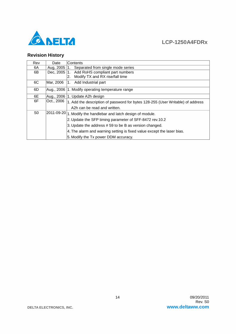
Revision History
Rev Date Contents 6A Aug, 2005 1. Separated from single mode series 6B Dec, 2005 1. Add RoHS compliant part numbers
2. Modify TX and RX rise/fall time
6C Mar, 2006 1. Add Industrial part
6D Aug., 2006 1. Modify operating temperature range
6E Aug., 2006 1. Update A2h design 6F Oct., 2006 1. Add the description of password for bytes 128-255 (User Writable) of address
A2h can be read and written. S0 2011-09-20 1. Modify the handlebar and latch design of module.
2. Update the SFP timing parameter of SFF-8472 rev.10.2
3. Update the address # 59 to be B as version changed.
4. The alarm and warning setting is fixed value except the laser bias.
5. Modify the Tx power DDM accuracy.