Embed Size (px)
Citation preview
1Mike Browne
BLM/PIC Hardware [email protected]@slac.stanford.edu
Mike Browne & John Dusatko
LCLS Undulator Beam loss MonitorPreliminary Design Review
BLM Control & Readout ElectronicsJanuary 24, 2008
Hardware Design Support Accelerator Controls DepartmentElectronics Engineering Section
Mike Browne, John Dusatko, Stephen Norum, Jeff Olsen, Chuck Yee
2Mike Browne
BLM/PIC Hardware [email protected]@slac.stanford.edu
Mike Browne & John Dusatko
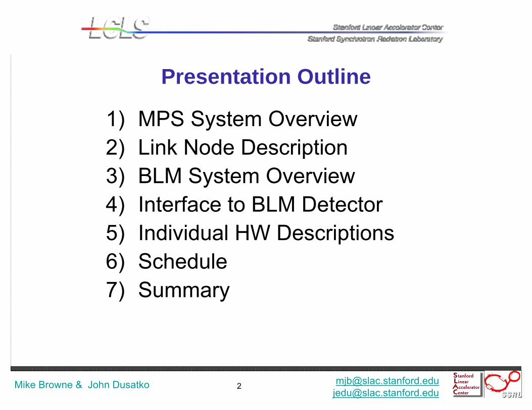
Presentation Outline
1) MPS System Overview2) Link Node Description3) BLM System Overview4) Interface to BLM Detector5) Individual HW Descriptions6) Schedule7) Summary
3Mike Browne
BLM/PIC Hardware [email protected]@slac.stanford.edu
Mike Browne & John Dusatko
MPS System Overview
4Mike Browne
BLM/PIC Hardware [email protected]@slac.stanford.edu
Mike Browne & John Dusatko
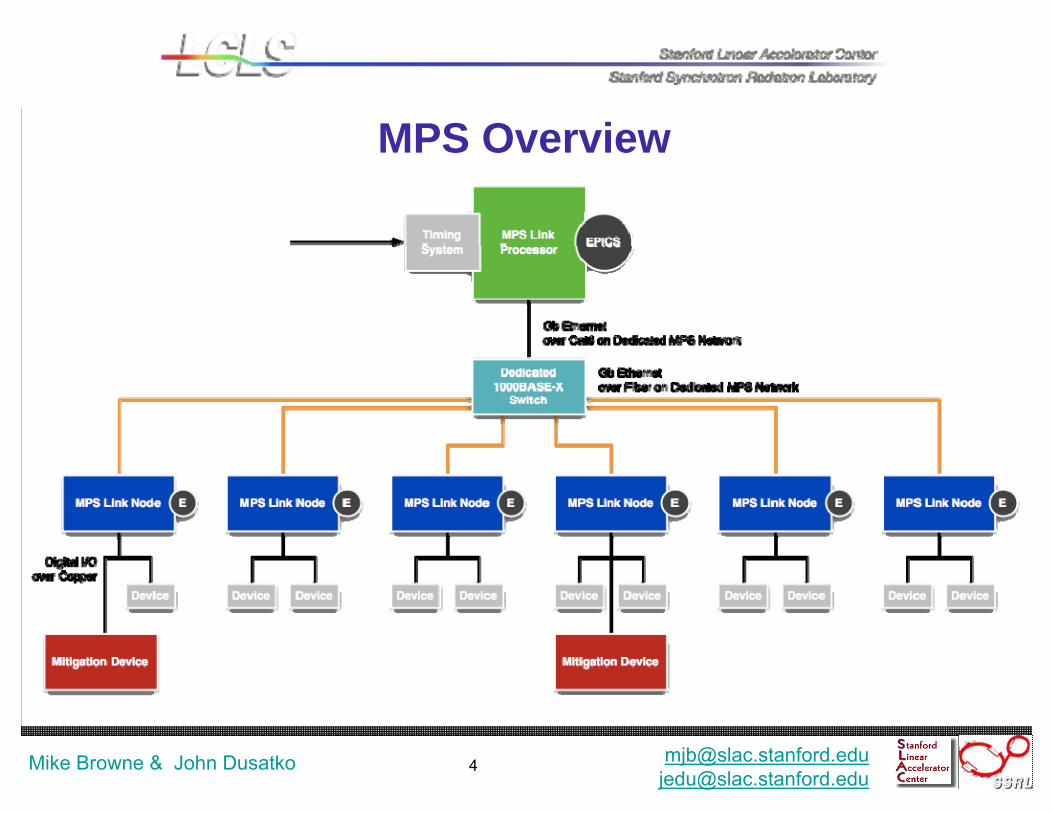
MPS Overview
5Mike Browne
BLM/PIC Hardware [email protected]@slac.stanford.edu
Mike Browne & John Dusatko
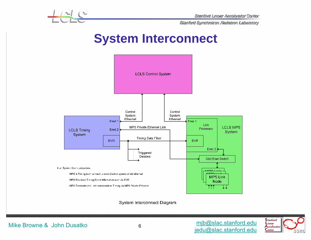
LCLS MPS System OverviewBasic Function: To provide a fault detection and beam rate limiting mechanism that protects critical LCLS accelerator components from excessive beam power, thereby preventing damage.
The System:• The LCLS MPS System is arranged in star topology, with one central Link
Processor running the MPS algorithm and multiple Link Nodes which interface to the machine status and mitigation devices. The MPS interfaces to the LCLS Timing System and the LCLS Control System.
• The Link Nodes interface to the Link Processor via a dedicated Gigabit Ethernet fiber link with a commercial G-bit Enet Switch (Cisco xxx).
• Machine status is collected by the Link Nodes and passed to the Link Processor. The Link Processor, according to its algorithm, processes the status information and responds appropriately: sending rate limiting commands to the Timing System and activating mitigation devices.
6Mike Browne
BLM/PIC Hardware [email protected]@slac.stanford.edu
Mike Browne & John Dusatko
System Interconnect
7Mike Browne
BLM/PIC Hardware [email protected]@slac.stanford.edu
Mike Browne & John Dusatko
LCLS MPS System Component Details
• LCLS MPS Link Processor:• Implemented in a VME Crate consisting of:
• MVME-6100 CPU running RTEMS & EPICS• Implements MPS Algorithm• Interfaces to EPICS Control System via Ethernet• Interfaces to Link Node• Interfaces for Timing System Event Generator
• MRF PMC-EVR• Interface to LCLS Timing System / Receives timing event data
• LCLS MPS Link Node• SLAC Custom-Designed Chassis (described next)
8Mike Browne
BLM/PIC Hardware [email protected]@slac.stanford.edu
Mike Browne & John Dusatko
MPS Link Node Description
9Mike Browne
BLM/PIC Hardware [email protected]@slac.stanford.edu
Mike Browne & John Dusatko
MPS Link Node
• The Link Node is the interface between the Link Processor and the Machine devices (sensors, valves, etc.)
• Custom Designed by SLAC LCLS Controls Group• Implemented in a 3U, 19-inch rack-mount chassis• Contains digital logic for status signal processing and
conditioning, local processor for EPICS interface, flexible I/O including both digital and analog
• Modular design: consists of main motherboard with MPS device I/O interface boards and general-purpose interface (Industry Pack) bus
10Mike Browne
BLM/PIC Hardware [email protected]@slac.stanford.edu
Mike Browne & John Dusatko
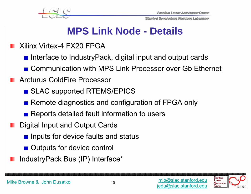
MPS Link Node - DetailsXilinx Virtex-4 FX20 FPGA
Interface to IndustryPack, digital input and output cardsCommunication with MPS Link Processor over Gb Ethernet
Arcturus ColdFire ProcessorSLAC supported RTEMS/EPICSRemote diagnostics and configuration of FPGA onlyReports detailed fault information to users
Digital Input and Output CardsInputs for device faults and statusOutputs for device control
IndustryPack Bus (IP) Interface*
11Mike Browne
BLM/PIC Hardware [email protected]@slac.stanford.edu
Mike Browne & John Dusatko
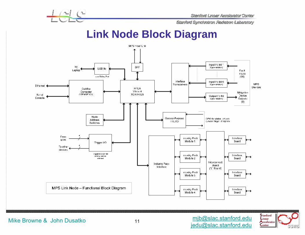
Link Node Block Diagram
12Mike Browne
BLM/PIC Hardware [email protected]@slac.stanford.edu
Mike Browne & John Dusatko
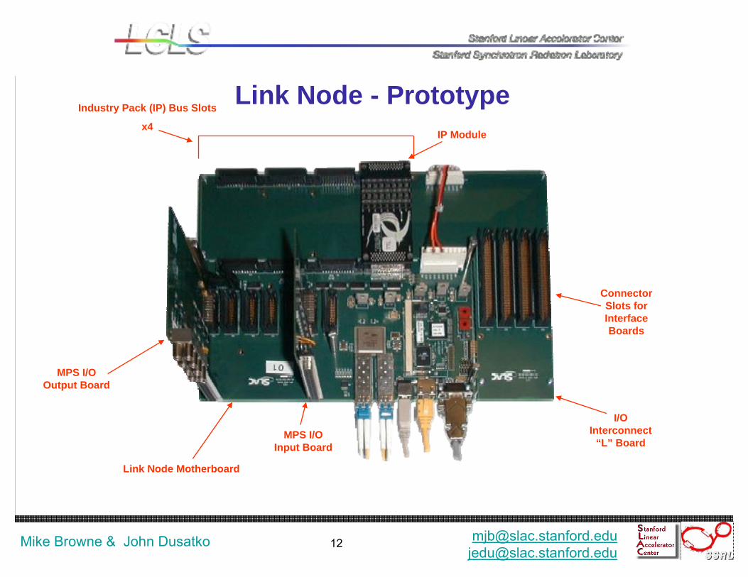
Link Node - Prototype
Link Node Motherboard
MPS I/O Output Board
MPS I/O Input Board
I/O Interconnect
“L” Board
Industry Pack (IP) Bus Slots
x4IP Module
Connector Slots for Interface Boards
13Mike Browne
BLM/PIC Hardware [email protected]@slac.stanford.edu
Mike Browne & John Dusatko
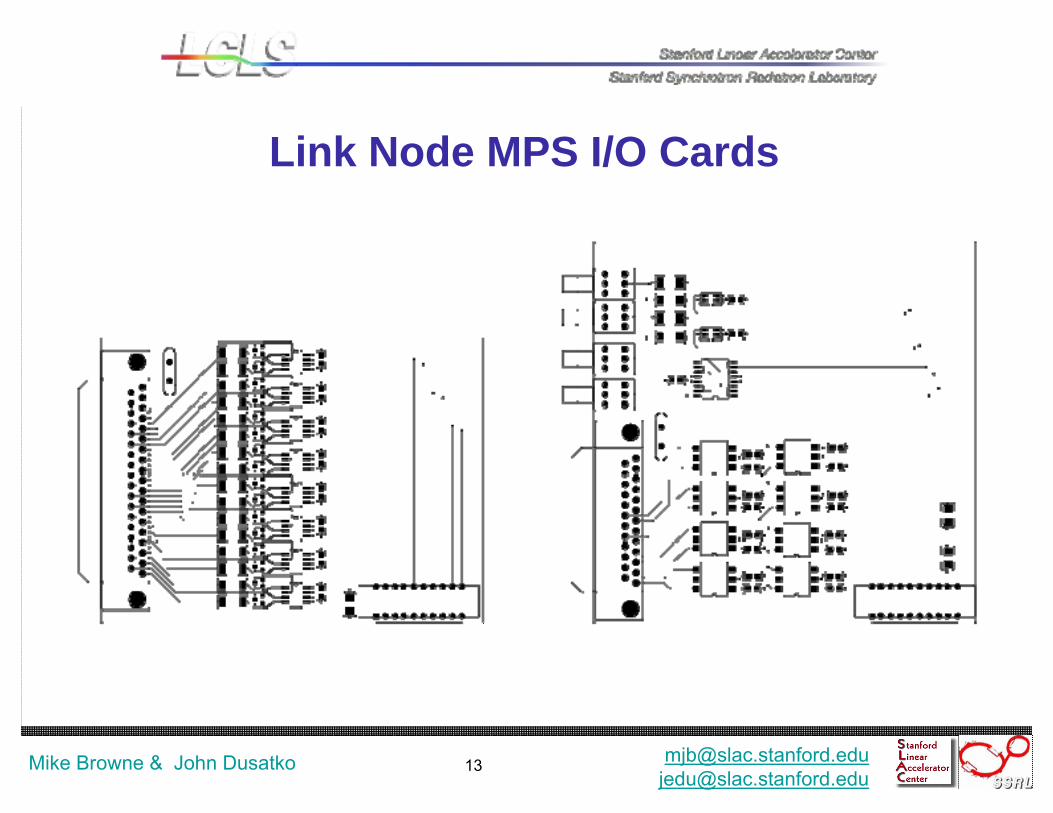
Link Node MPS I/O Cards
14Mike Browne
BLM/PIC Hardware [email protected]@slac.stanford.edu
Mike Browne & John Dusatko
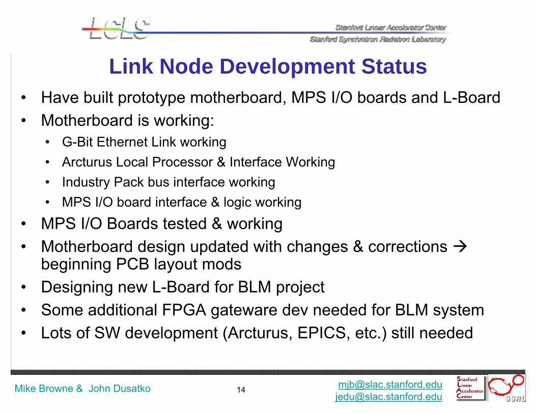
Link Node Development Status• Have built prototype motherboard, MPS I/O boards and L-Board• Motherboard is working:
• G-Bit Ethernet Link working• Arcturus Local Processor & Interface Working• Industry Pack bus interface working• MPS I/O board interface & logic working
• MPS I/O Boards tested & working• Motherboard design updated with changes & corrections
beginning PCB layout mods• Designing new L-Board for BLM project• Some additional FPGA gateware dev needed for BLM system• Lots of SW development (Arcturus, EPICS, etc.) still needed
15Mike Browne
BLM/PIC Hardware [email protected]@slac.stanford.edu
Mike Browne & John Dusatko
Beam Loss Monitor Readout System
16Mike Browne
BLM/PIC Hardware [email protected]@slac.stanford.edu
Mike Browne & John Dusatko
BLM Readout System: Proposed DesignDesign Philosophy:
Since the BLM is going to be an MPS device, why not integrate directly into the MPS System?Using the Link Node Chassis with a mix of custom and COTS HW, develop a solution that can control and read out the the BLM detector and provide a beam loss status signal to the LCLS MPS system as well as beam loss measurement data to the LCLS control system
Use Link Node toGenerate Beam Loss FaultProvide analog readouts to control systemSet threshold levelsControl PMT HV power suppliesGenerate “heartbeat” test pulseSynchronized to beam using trigger from LCLC Timing System
17Mike Browne
BLM/PIC Hardware [email protected]@slac.stanford.edu
Mike Browne & John Dusatko
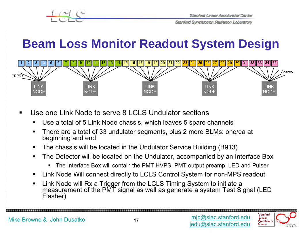
Beam Loss Monitor Readout System Design
Use one Link Node to serve 8 LCLS Undulator sectionsUse a total of 5 Link Node chassis, which leaves 5 spare channelsThere are a total of 33 undulator segments, plus 2 more BLMs: one/ea at beginning and endThe chassis will be located in the Undulator Service Building (B913)The Detector will be located on the Undulator, accompanied by an Interface Box
The Interface Box will contain the PMT HVPS, PMT output preamp, LED and PulserLink Node Will connect directly to LCLS Control System for non-MPS readoutLink Node will Rx a Trigger from the LCLS Timing System to initiate a measurement of the PMT signal as well as generate a system Test Signal (LED Flasher)
18Mike Browne
BLM/PIC Hardware [email protected]@slac.stanford.edu
Mike Browne & John Dusatko
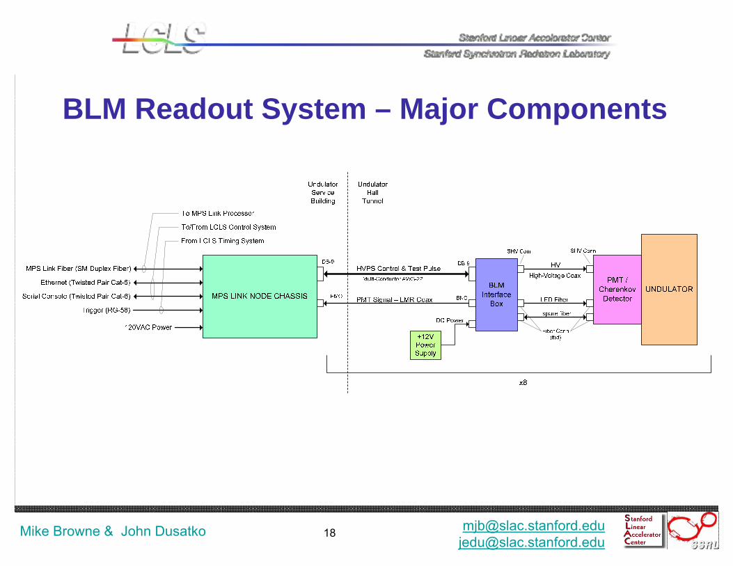
BLM Readout System – Major Components
19Mike Browne
BLM/PIC Hardware [email protected]@slac.stanford.edu
Mike Browne & John Dusatko
BLM System – Interconnect
• Detector:• Cherenkov Light (Quartz Crystal)• PMT Readout• Detector Local Support functions done by BLM
Interface Box (This Review – Tony Pietryla/ANL)• BLM Interface Box:
• Contains HPVS for PMT• Preamp with pulse shaping & line driver for PMT signal• Test LED & Driver for general heartbeat / detector health
test
20Mike Browne
BLM/PIC Hardware [email protected]@slac.stanford.edu
Mike Browne & John Dusatko
BLM System – Interconnect Signals
• BLM IFC Box to Link Node Signals:PMT HVPS Control (Analog-DC: 0...+5V)PMT HPVS Readback (Analog-DC: 0…+5V)Test Trigger Pulse (Digital: 100ns min / RS-485 Diff’l)►These signals are sent on twisted-pair, individually shielded wires on a
multi-conductor cable with overall shield / DB-9 connectors
PMT Signal / High-Speed Voltage Pulse / 0...+1.5V• Sent over LMR-400 double-shielded coax / SMA connectors
Maximum System Cable Length = 300 Feet
21Mike Browne
BLM/PIC Hardware [email protected]@slac.stanford.edu
Mike Browne & John Dusatko
BLM System – Grounding & ShieldingHandling of Grounding & Shielding between boxes:
BLM Interface Box:Signal returns are connected to internal groundIndividual Pair Shields are connected to same ground
► Returns & Shields are NOT connected to box common Gnd / but there is provision to do so
Overall cable Shield NOT connected at this side
Link Node Chassis:Control Signals Returns are connected to system ground at BLM Interface BoardPMT Signal Return connected to system GndIndividual Pair Signal Shields are connected to system ground thru ferrite beads / shields connections can be broken if needed (if Gnd loops are present)Overall cable Shield is connected to system ground thru ferrite bead / provision to open shield if needed
22Mike Browne
BLM/PIC Hardware [email protected]@slac.stanford.edu
Mike Browne & John Dusatko
BLM System HW: Link Node
23Mike Browne
BLM/PIC Hardware [email protected]@slac.stanford.edu
Mike Browne & John Dusatko
Link Node HW: ImplementationThe Link Node Will Contain A mixture of COTS & custom HW to implement the BLM readout & control
COTS HW:COTS DAC: (Acromag IP-231) for HVPS Control / 16-Channel, 16-BitsCOTS ADC: (Acromag IP-330A) for HVPS Readback / 16-Channel, 16-Bits
BOTH of these module are already in use in the LCLS Control System
Custom HW:Custom ADC for PMT Signal Acquisition, Accumulated Dose Processing & Test Trigger GenerationCustom Interface Boards In Link Node for IFC between BLM Ifc Box and Link NodeRe-Design of Link Node L-Board to map signals between IP-Modules and BLM Interface boards
24Mike Browne
BLM/PIC Hardware [email protected]@slac.stanford.edu
Mike Browne & John Dusatko
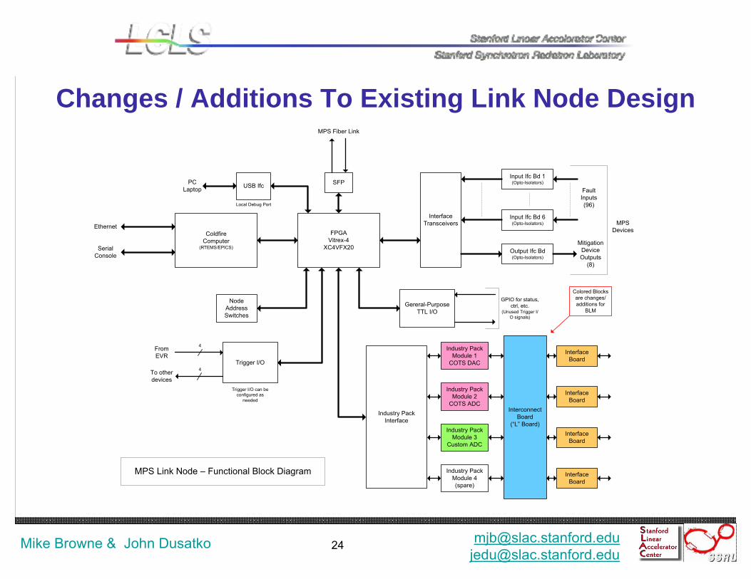
Changes / Additions To Existing Link Node Design
ColdfireComputer
(RTEMS/EPICS)
FPGAVitrex-4
XC4VFX20
Interface Transceivers
MPS Fiber Link
SFP
Gereral-Purpose TTL I/O
Output Ifc Bd(Opto-Isolators)
MPS Link Node – Functional Block Diagram
Ethernet MPS Devices
Fault Inputs(96)
Mitigation Device Outputs
(8)
Industry PackInterface
Industry PackModule 1
COTS DAC
Interface Board
Industry PackModule 2
COTS ADC
GPIO for status, ctrl, etc.
(Unused Trigger I/O signals)
Industry PackModule 3
Custom ADC
Industry PackModule 4(spare)
Input Ifc Bd 6(Opto-Isolators)
Input Ifc Bd 1(Opto-Isolators)
Trigger I/O
USB Ifc
4
4
Trigger I/O can be configured as
needed
From EVR
To other devices
PC Laptop
Local Debug Port
Node Address Switches
Interface Board
Interface Board
Interface Board
InterconnectBoard
(“L” Board)
Serial Console
Colored Blocks are changes/additions for
BLM
25Mike Browne
BLM/PIC Hardware [email protected]@slac.stanford.edu
Mike Browne & John Dusatko
Link Node BLM Hardware
• The Individual custom components will now be described:
►BLM Interface Board ►Interconnect L-Board►Custom IP-ADC Board
26Mike Browne
BLM/PIC Hardware [email protected]@slac.stanford.edu
Mike Browne & John Dusatko
BLM Interface Board
27Mike Browne
BLM/PIC Hardware [email protected]@slac.stanford.edu
Mike Browne & John Dusatko
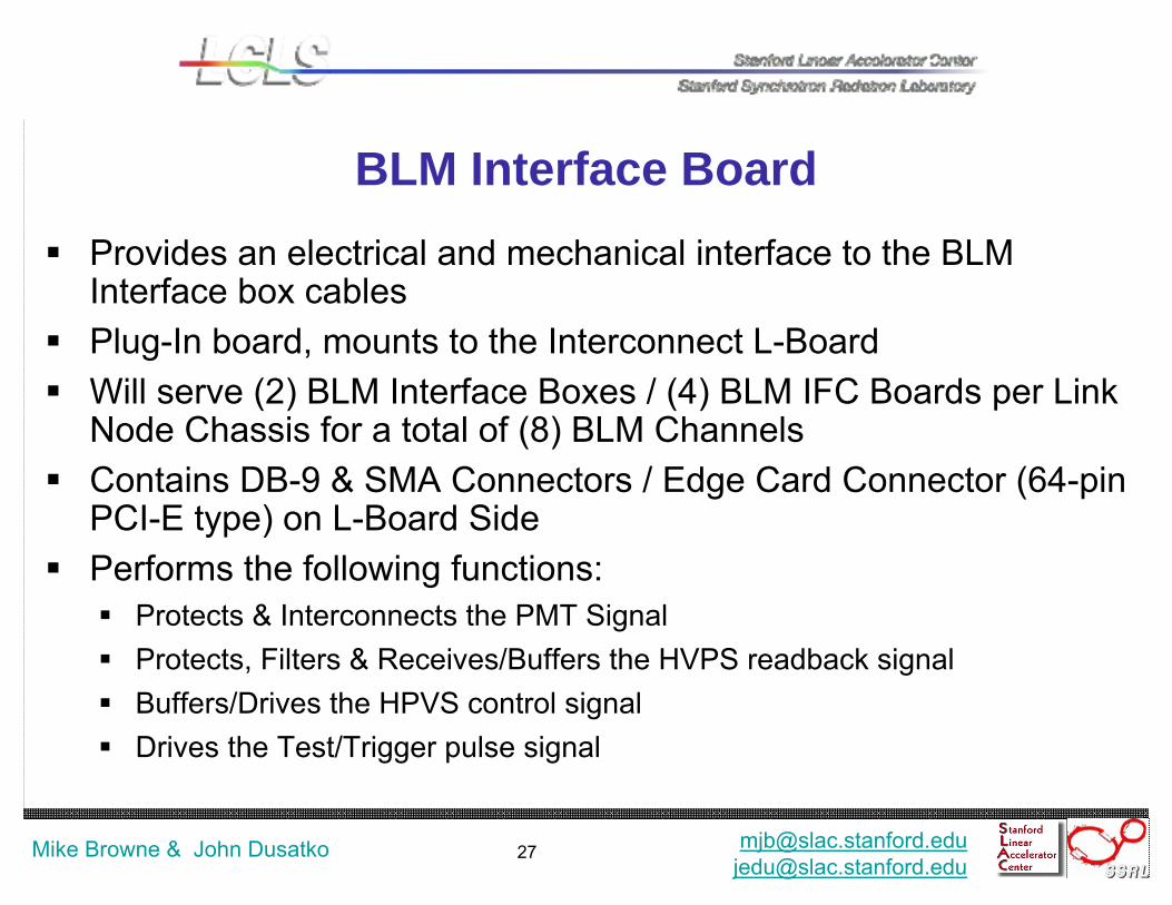
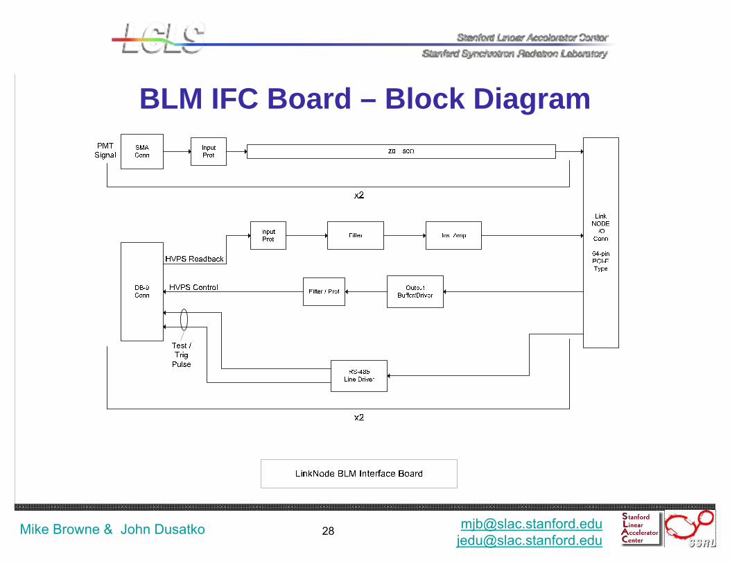
BLM Interface BoardProvides an electrical and mechanical interface to the BLM Interface box cablesPlug-In board, mounts to the Interconnect L-BoardWill serve (2) BLM Interface Boxes / (4) BLM IFC Boards per LinkNode Chassis for a total of (8) BLM ChannelsContains DB-9 & SMA Connectors / Edge Card Connector (64-pin PCI-E type) on L-Board SidePerforms the following functions:
Protects & Interconnects the PMT SignalProtects, Filters & Receives/Buffers the HVPS readback signalBuffers/Drives the HPVS control signalDrives the Test/Trigger pulse signal
28Mike Browne
BLM/PIC Hardware [email protected]@slac.stanford.edu
Mike Browne & John Dusatko
BLM IFC Board – Block Diagram
29Mike Browne
BLM/PIC Hardware [email protected]@slac.stanford.edu
Mike Browne & John Dusatko
• Schematic is 90% complete• Will begin layout prep week of 1-28-2008• Layout will take approx. 1 week• No long-lead components• Prototype testing to start Mid-Feb 2008
BLM IFC Board – Status

30Mike Browne
BLM/PIC Hardware [email protected]@slac.stanford.edu
Mike Browne & John Dusatko
Interconnect L-Board
31Mike Browne
BLM/PIC Hardware [email protected]@slac.stanford.edu
Mike Browne & John Dusatko
Link Node Interconnect L-Board• Provides an interconnect medium between the IP Module’s I/O
signals and the BLM Interface board /• Can be thought of as a kind of “backplane” for Link Node boards• Also contains power connector and trigger connectors • Ties together and routes all of the I/O signals to their appropriate
destinations• Very simple, flexible design / consists of mainly connectors and
traces• Critical signals (analog & digital) are routed away from each other
/ copious use of Gnd planes / power filtering done at pwr entry point
• PMT signals are routed as 50Ω stripline traces
32Mike Browne
BLM/PIC Hardware [email protected]@slac.stanford.edu
Mike Browne & John Dusatko
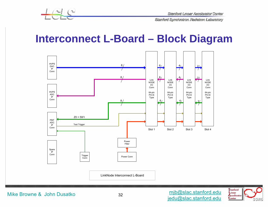
Interconnect L-Board – Block Diagram
HVPSDAC
IP Conn
LinkNode Interconnect L-Board
LinkNODE
I/OConn
64-pinPCI-EType
HVPSADC
IP Conn
PMTADC
IP Conn
SpareIP
Conn
LinkNODE
I/OConn
64-pinPCI-EType
LinkNODE
I/OConn
64-pinPCI-EType
LinkNODE
I/OConn
64-pinPCI-EType
Power Conn
Slot 1 Slot 2 Slot 3 Slot 4
TriggerConn
Power Filter
8 6 4 2
6 4 2
6 4 2
8
8
Z0 = 50
Test Trigger
33Mike Browne
BLM/PIC Hardware [email protected]@slac.stanford.edu
Mike Browne & John Dusatko
Interconnect L-Board -- Status
• Schematic started, 10% complete• Will begin layout 2-20-2008• Layout will take approx. 1 week• No long-lead components• PCB Design is part of Link Node Design File /
Will be submitted with Link Node for Fab / late -Feb 2008
• Some Link Node Chassis are currently being fabricated without the L-Board.
34Mike Browne
BLM/PIC Hardware [email protected]@slac.stanford.edu
Mike Browne & John Dusatko
Custom IP-ADC
35Mike Browne
BLM/PIC Hardware [email protected]@slac.stanford.edu
Mike Browne & John Dusatko
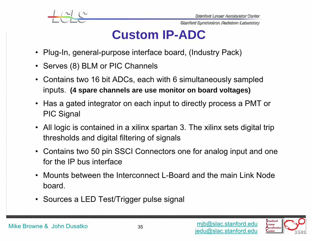
• Plug-In, general-purpose interface board, (Industry Pack)
• Serves (8) BLM or PIC Channels
• Contains two 16 bit ADCs, each with 6 simultaneously sampled inputs. (4 spare channels are use monitor on board voltages)
• Has a gated integrator on each input to directly process a PMT or PIC Signal
• All logic is contained in a xilinx spartan 3. The xilinx sets digital trip thresholds and digital filtering of signals
• Contains two 50 pin SSCI Connectors one for analog input and onefor the IP bus interface
• Mounts between the Interconnect L-Board and the main Link Node board.
• Sources a LED Test/Trigger pulse signal
Custom IP-ADC
36Mike Browne
BLM/PIC Hardware [email protected]@slac.stanford.edu
Mike Browne & John Dusatko
CUSTOM IP-ADC (BLM OPERATION)
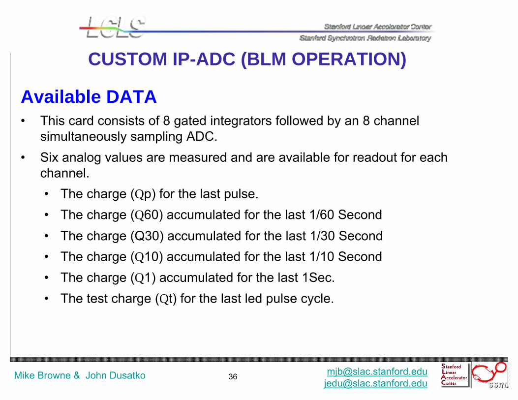
Available DATA• This card consists of 8 gated integrators followed by an 8 channel
simultaneously sampling ADC.• Six analog values are measured and are available for readout for each
channel.• The charge (Qp) for the last pulse.• The charge (Q60) accumulated for the last 1/60 Second• The charge (Q30) accumulated for the last 1/30 Second• The charge (Q10) accumulated for the last 1/10 Second• The charge (Q1) accumulated for the last 1Sec.• The test charge (Qt) for the last led pulse cycle.
37Mike Browne
BLM/PIC Hardware [email protected]@slac.stanford.edu
Mike Browne & John Dusatko
CUSTOM IP-ADC (BLM OPERATION)
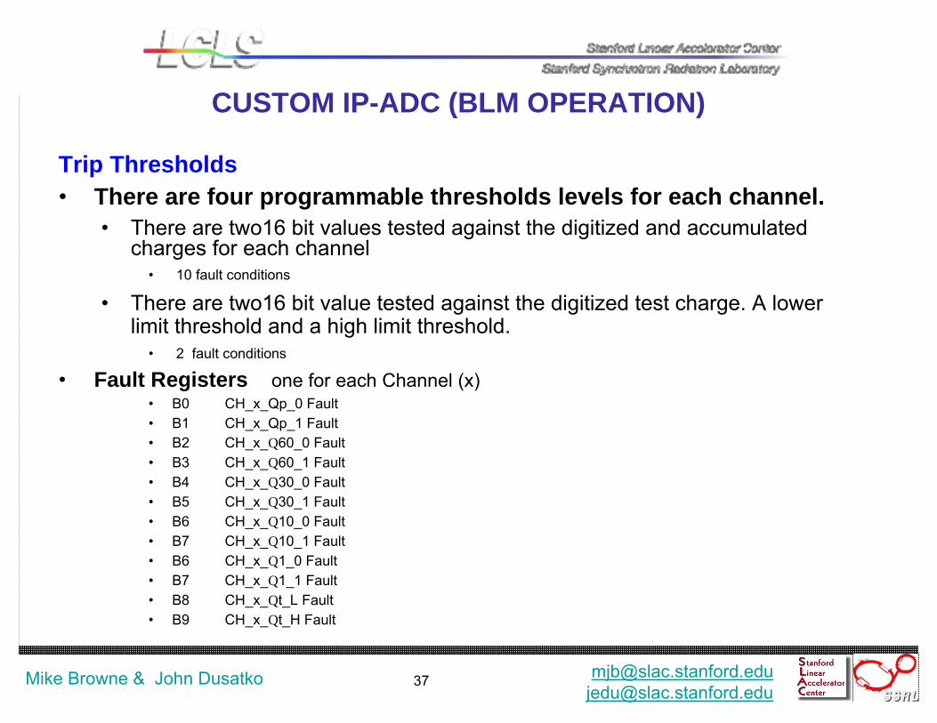
Trip Thresholds• There are four programmable thresholds levels for each channel.
• There are two16 bit values tested against the digitized and accumulated charges for each channel
• 10 fault conditions
• There are two16 bit value tested against the digitized test charge. A lower limit threshold and a high limit threshold.
• 2 fault conditions
• Fault Registers one for each Channel (x)• B0 CH_x_Qp_0 Fault• B1 CH_x_Qp_1 Fault• B2 CH_x_Q60_0 Fault• B3 CH_x_Q60_1 Fault• B4 CH_x_Q30_0 Fault• B5 CH_x_Q30_1 Fault• B6 CH_x_Q10_0 Fault• B7 CH_x_Q10_1 Fault• B6 CH_x_Q1_0 Fault• B7 CH_x_Q1_1 Fault• B8 CH_x_Qt_L Fault• B9 CH_x_Qt_H Fault
38Mike Browne
BLM/PIC Hardware [email protected]@slac.stanford.edu
Mike Browne & John Dusatko
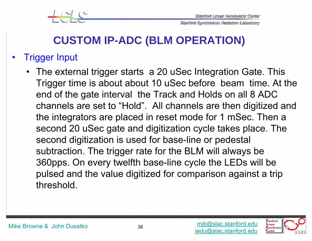
• Trigger Input• The external trigger starts a 20 uSec Integration Gate. This
Trigger time is about about 10 uSec before beam time. At the end of the gate interval the Track and Holds on all 8 ADC channels are set to “Hold”. All channels are then digitized and the integrators are placed in reset mode for 1 mSec. Then a second 20 uSec gate and digitization cycle takes place. The second digitization is used for base-line or pedestal subtraction. The trigger rate for the BLM will always be 360pps. On every twelfth base-line cycle the LEDs will be pulsed and the value digitized for comparison against a trip threshold.
CUSTOM IP-ADC (BLM OPERATION)
39Mike Browne
BLM/PIC Hardware [email protected]@slac.stanford.edu
Mike Browne & John Dusatko
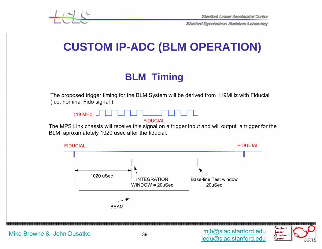
BLM Timing
FIDUCIAL FIDUCIAL
INTEGRATIONWINDOW = 20uSec
1020 uSec
The proposed trigger timing for the BLM System will be derived from 119MHz with Fiducial ( i.e. nominal Fido signal )
FIDUCIAL119 MHz
The MPS Link chassis will receive this signal on a trigger input and will output a trigger for the BLM aproximatetely 1020 usec after the fiducial.
Base-line Test window20uSec
BEAM
CUSTOM IP-ADC (BLM OPERATION)
40Mike Browne
BLM/PIC Hardware [email protected]@slac.stanford.edu
Mike Browne & John Dusatko
CUSTOM IP-ADC
360 Word Shift Register
Q1
D1
ADCDATA
UPDATE CLK
1 SecondAverage
Q12
Q36
+Q6
Q360
+
-
Q1D1
Q330
BASE LINEDATA +
+
-
DIVIDE BY330
Base Line Subtraction
330 Word Shift Register
Qp
Q60
Q30
Q10
Q1
Comparators Fault Outputs
++
-
++
-
+-
++
-
+
BL CLK
41Mike Browne
BLM/PIC Hardware [email protected]@slac.stanford.edu
Mike Browne & John Dusatko
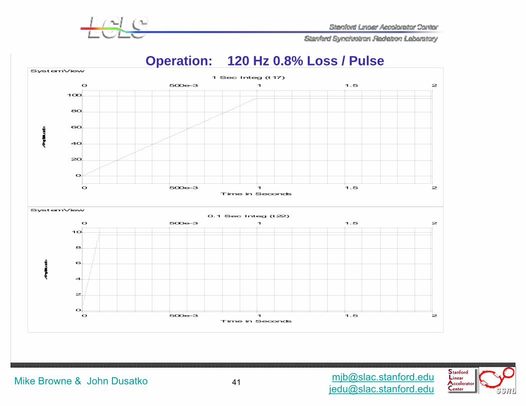
Operation: 120 Hz 0.8% Loss / PulseSystemView
0
0
500e-3
500e-3
1
1
1.5
1.5
2
2
100
80
60
40
20
0
Amplitude
Time in Seconds
1 Sec Integ (t17)
SystemView
0
0
500e-3
500e-3
1
1
1.5
1.5
2
2
10
8
6
4
2
0
Amplitude
Time in Seconds
0.1 Sec Integ (t22)
42Mike Browne
BLM/PIC Hardware [email protected]@slac.stanford.edu
Mike Browne & John Dusatko
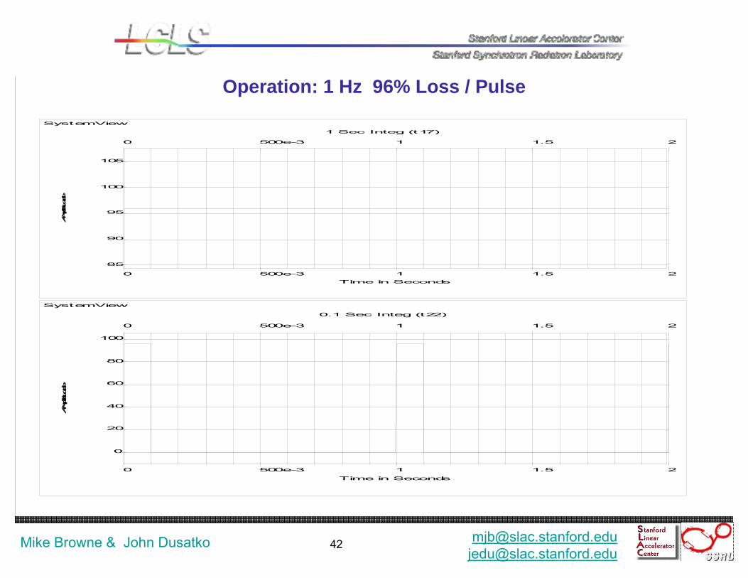
Operation: 1 Hz 96% Loss / PulseSystemView
0
0
500e-3
500e-3
1
1
1.5
1.5
2
2
105
100
95
90
85
Amplitude
Time in Seconds
1 Sec Integ (t17)
SystemView
0
0
500e-3
500e-3
1
1
1.5
1.5
2
2
100
80
60
40
20
0
Amplitude
Time in Seconds
0.1 Sec Integ (t22)
44Mike Browne
BLM/PIC Hardware [email protected]@slac.stanford.edu
Mike Browne & John Dusatko
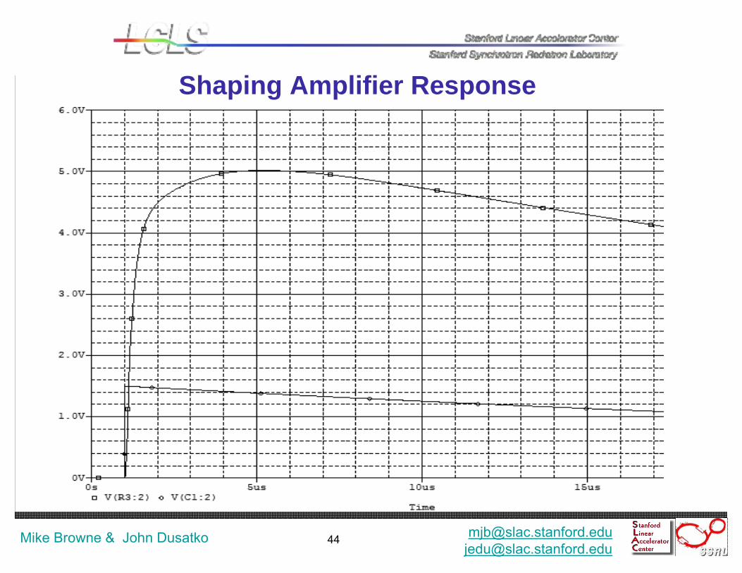
Shaping Amplifier Response
45Mike Browne
BLM/PIC Hardware [email protected]@slac.stanford.edu
Mike Browne & John Dusatko
CUSTOM IP-ADC STATUS
• Schematic almost completed, 98% complete• Will begin layout prep week of 2-4-2008• Layout will take approx. 2 weeks• No long-lead components• Xilinx code just started, 10%• First production unit should arive 3 -10 – 2008
• Xilinx code needs to be ready at that time.