Embed Size (px)
Citation preview
1LC3-ControlPage 1
ECE 238L
LC-3 Control and FSM Design
LC3-3Page 2
© 2006ECE238L
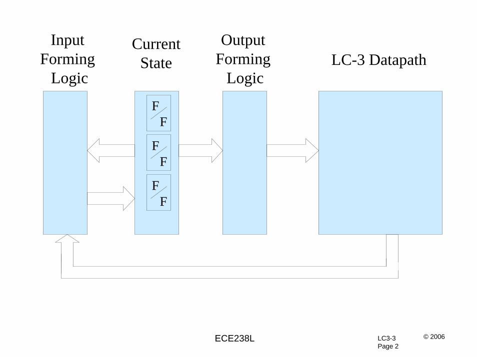
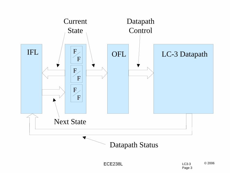
Output Forming
Logic
CurrentState
Input Forming
Logic
FF
FF
FF
LC-3 Datapath
LC3-3Page 3
© 2006ECE238L
OFLIFL
FF
FF
FF
LC-3 Datapath
Next State
DatapathControl
CurrentState
Datapath Status
LC3-3Page 4
© 2006ECE238L
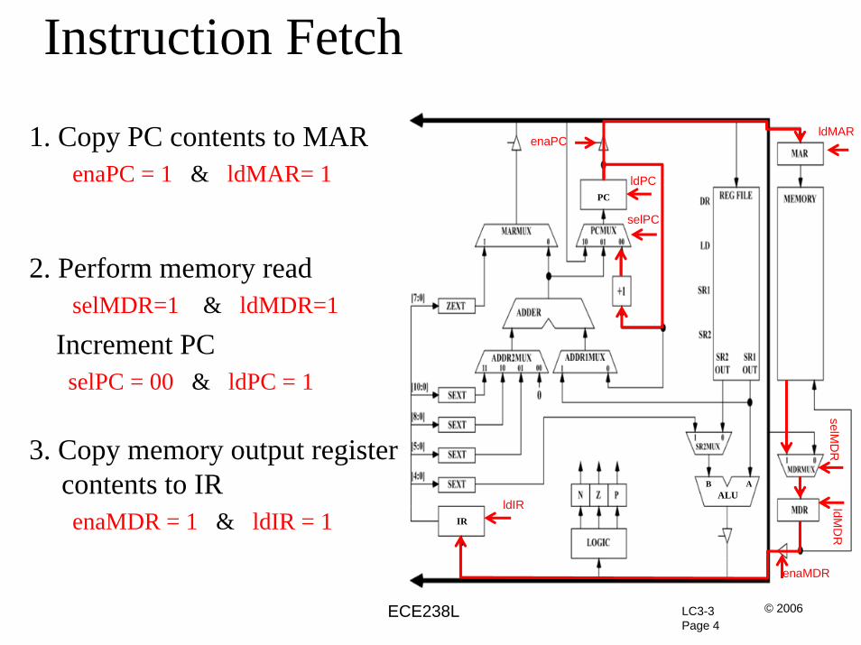
Instruction Fetch
1. Copy PC contents to MARenaPC = 1 & ldMAR= 1
2. Perform memory readselMDR=1 & ldMDR=1
Increment PCselPC = 00 & ldPC = 1
3. Copy memory output register contents to IRenaMDR = 1 & ldIR = 1 IR
PC
ALU
enaPCldMAR
ldPC
selPC
selMD
RldM
DR
enaMDR
ldIR
AB
LC3-3Page 5
© 2006ECE238L
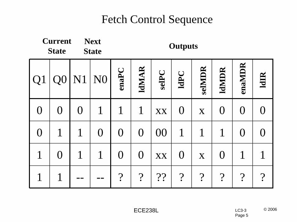
Q1 Q0 N1 N0
0 0
0
1
?
1
0
?
1
0
1
--
0
0
1
1
x 0
0
1
?
1
x
?
0 0 1 1 xx 0
1 1 0 0 00 1
0 1 0 0 xx 0
1 -- ? ? ?? ?
enaP
C
ldM
AR
selP
C
ldPC
enaM
DR
ldIR
CurrentState
NextState Outputs
Fetch Control Sequence
selM
DR
ldM
DR
LC3-3Page 6
© 2006ECE238L
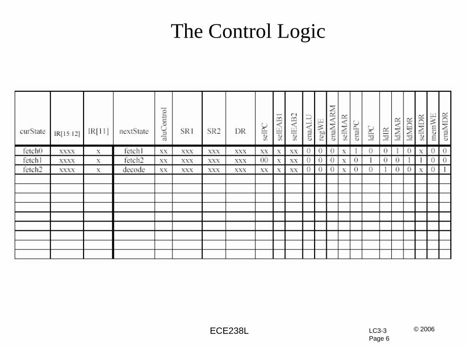
The Control Logic
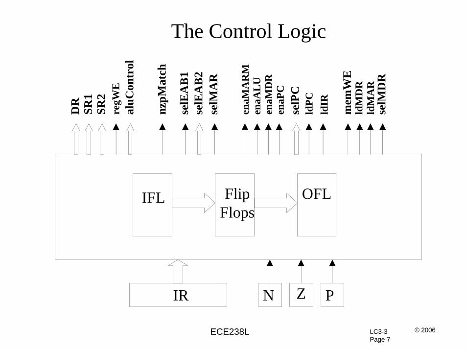
LC3-3Page 7
© 2006ECE238L
The Control Logic
IFL FlipFlops
OFL
IR N Z P
DR
SR2
selM
AR
selP
C
aluC
ontr
ol
SR1
ldM
DR
ldM
AR
regW
E
ldPC
ldIR
mem
WE
enaM
AR
Men
aAL
Uen
aMD
Ren
aPC
selE
AB
1se
lEA
B2
selM
DR
nzpM
atch
8LC3-ControlPage 8
ECE 238L
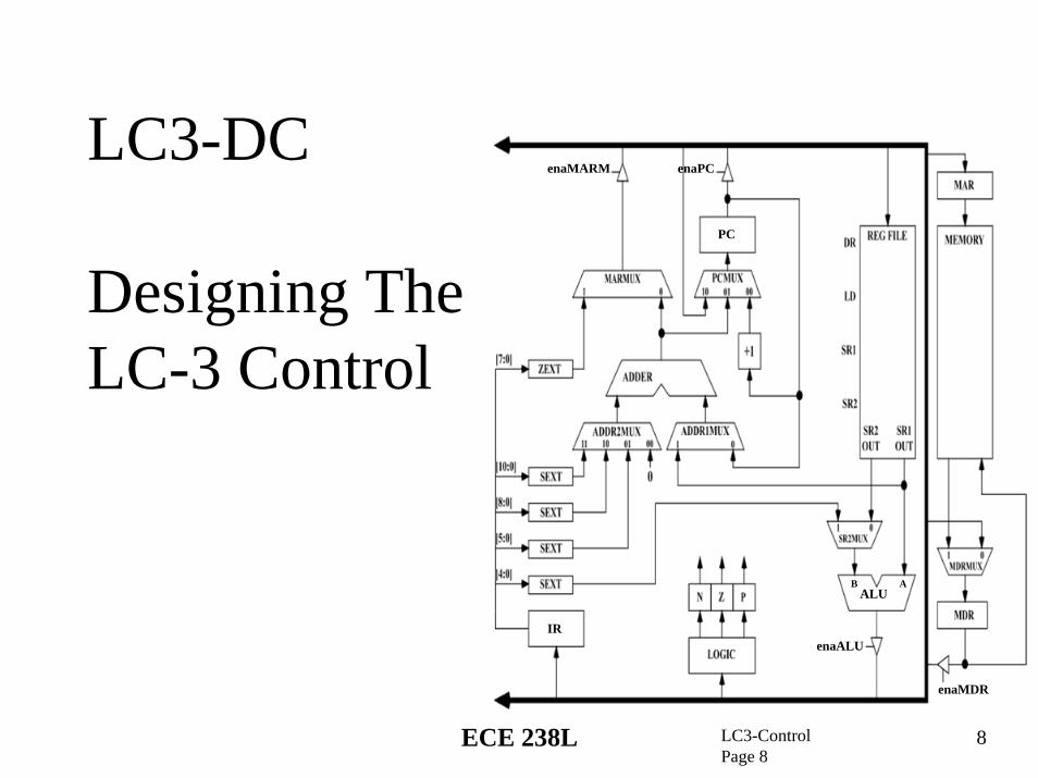
LC3-DC
Designing TheLC-3 Control
IR
PC
enaMARM enaPC
enaALU
enaMDR
ALUAB
LC3-3Page 9
© 2006ECE238L
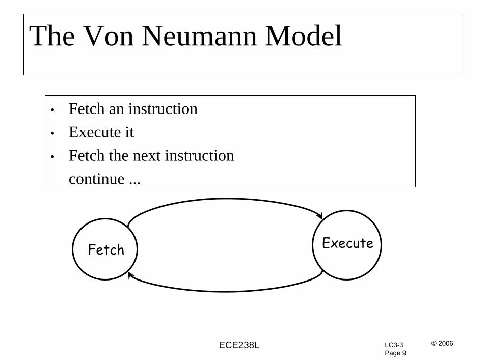
The Von Neumann Model
• Fetch an instruction• Execute it• Fetch the next instruction
continue ...
Fetch Execute
LC3-3Page 10
© 2006ECE238L
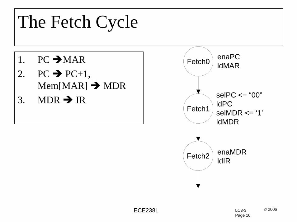
The Fetch Cycle
1. PC MAR2. PC PC+1,
Mem[MAR] MDR3. MDR IR
Fetch0
Fetch1
Fetch2
enaPCldMAR
enaMDRldIR
selPC <= “00”ldPCselMDR <= ‘1’ldMDR
LC3-3Page 11
© 2006ECE238L
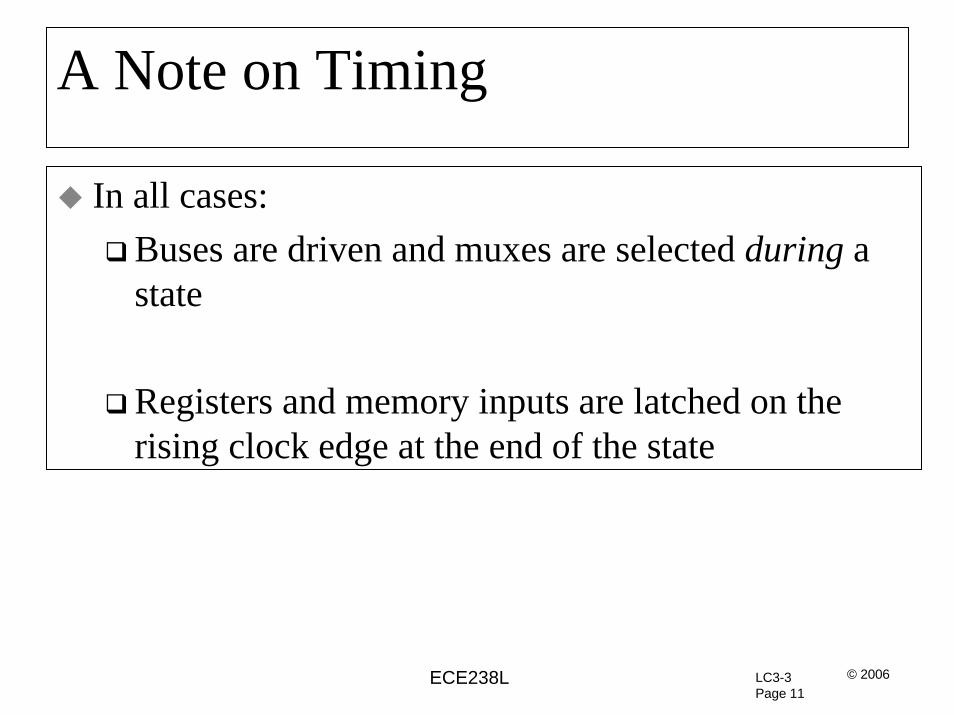
A Note on Timing
In all cases:Buses are driven and muxes are selected during a state
Registers and memory inputs are latched on the rising clock edge at the end of the state
LC3-3Page 12
© 2006ECE238L
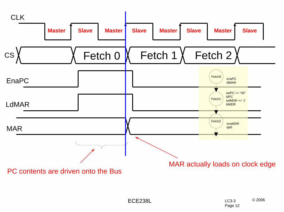
Fetch 0 Fetch 1 Fetch 2
PC contents are driven onto the Bus
EnaPC
LdMAR
CLK
CS
MAR actually loads on clock edge
MAR
Fetch0
Fetch1
Fetch2
enaPCldMAR
enaMDRldIR
selPC <= “00”ldPCselMDR <= ‘1’ldMDR
Master Master Master MasterSlave Slave Slave Slave

LC3-3Page 13
© 2006ECE238L
Fetch 0 Fetch 1 Fetch 2
Memory is being accessedand generates its output
LdMDR
CLK
CS
MDR actually loads on clock edge
MDR
LdIR
Fetch0
Fetch1
Fetch2
enaPCldMAR
enaMDRldIR
selPC <= “00”ldPCselMDR <= ‘1’ldMDR
Master Master Master MasterSlave Slave Slave Slave
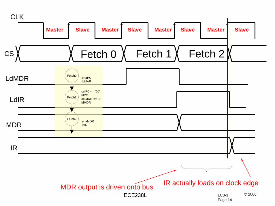
LC3-3Page 14
© 2006ECE238L
Fetch 0 Fetch 1 Fetch 2
MDR output is driven onto bus
LdMDR
CLK
CS
IR actually loads on clock edge
MDR
LdIR
IR
Fetch0
Fetch1
Fetch2
enaPCldMAR
enaMDRldIR
selPC <= “00”ldPCselMDR <= ‘1’ldMDR
Master Master Master MasterSlave Slave Slave Slave
LC3-3Page 15
© 2006ECE238L
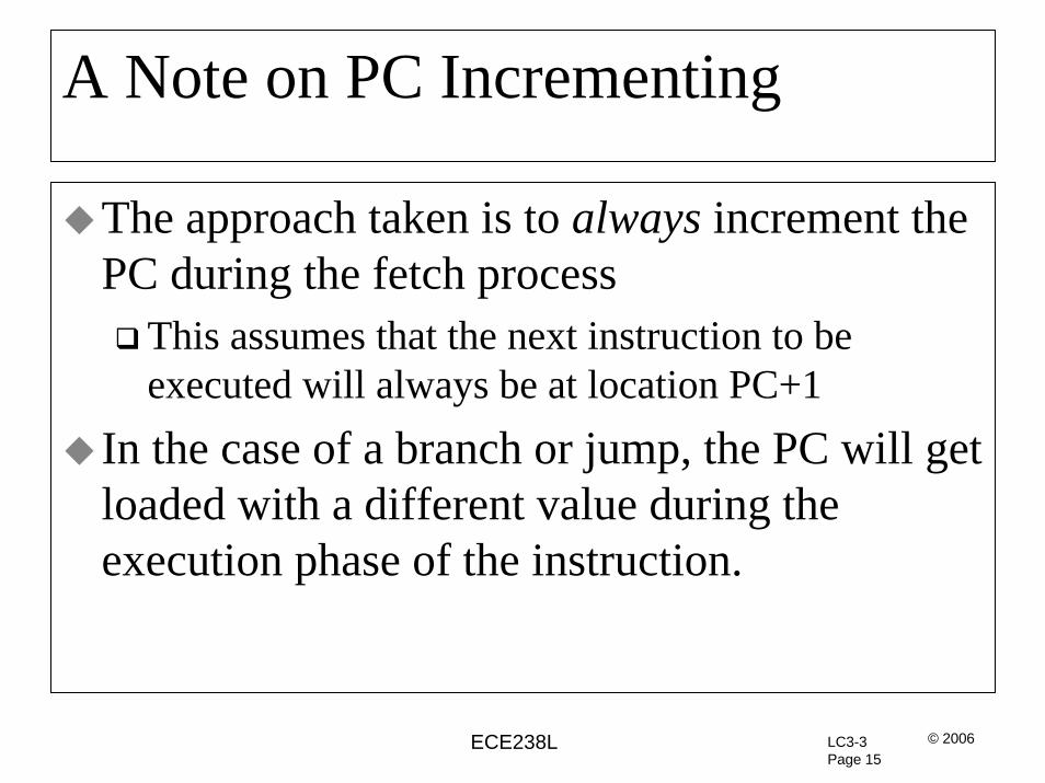
A Note on PC Incrementing
The approach taken is to always increment the PC during the fetch process
This assumes that the next instruction to be executed will always be at location PC+1
In the case of a branch or jump, the PC will get loaded with a different value during the execution phase of the instruction.
LC3-3Page 16
© 2006ECE238L
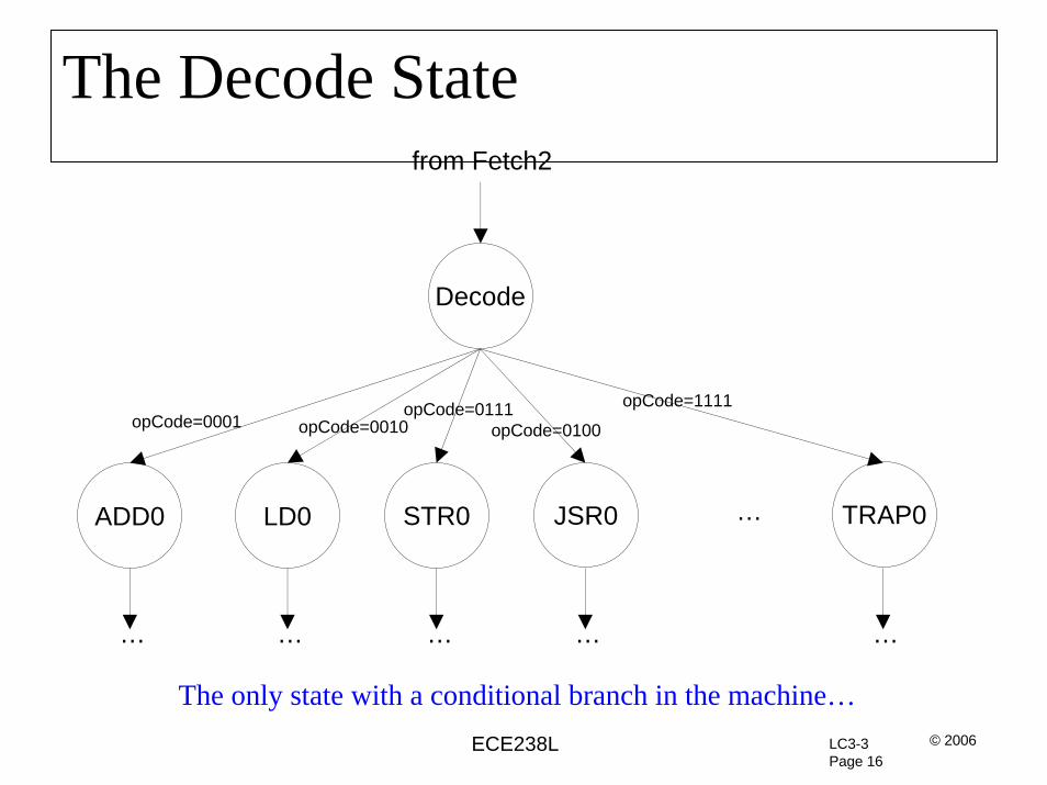
The Decode State
Decode
from Fetch2
ADD0 LD0 STR0 JSR0 TRAP0…
… … … … …
opCode=0001 opCode=0010opCode=0111
opCode=0100
opCode=1111
The only state with a conditional branch in the machine…
17LC3-ControlPage 17
ECE 238L
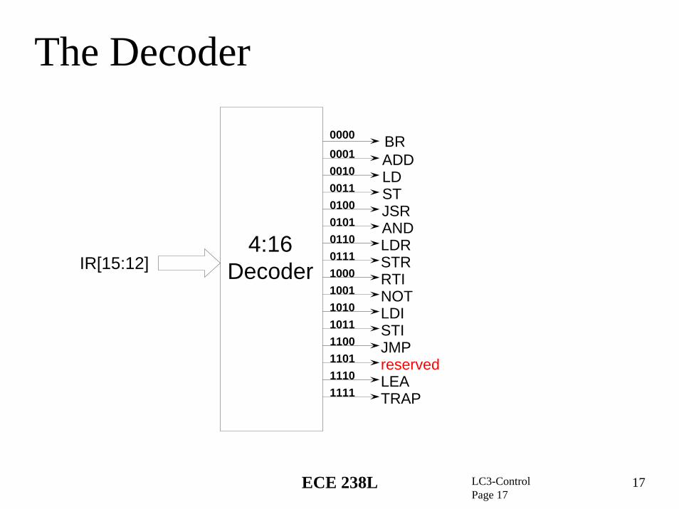
The Decoder
IR[15:12]
BRADDLDSTJSRANDLDRSTRRTINOTLDISTIJMPreservedLEATRAP
0000000100100011010001010110011110001001101010111100110111101111
4:16Decoder
LC3-3Page 18
© 2006ECE238L
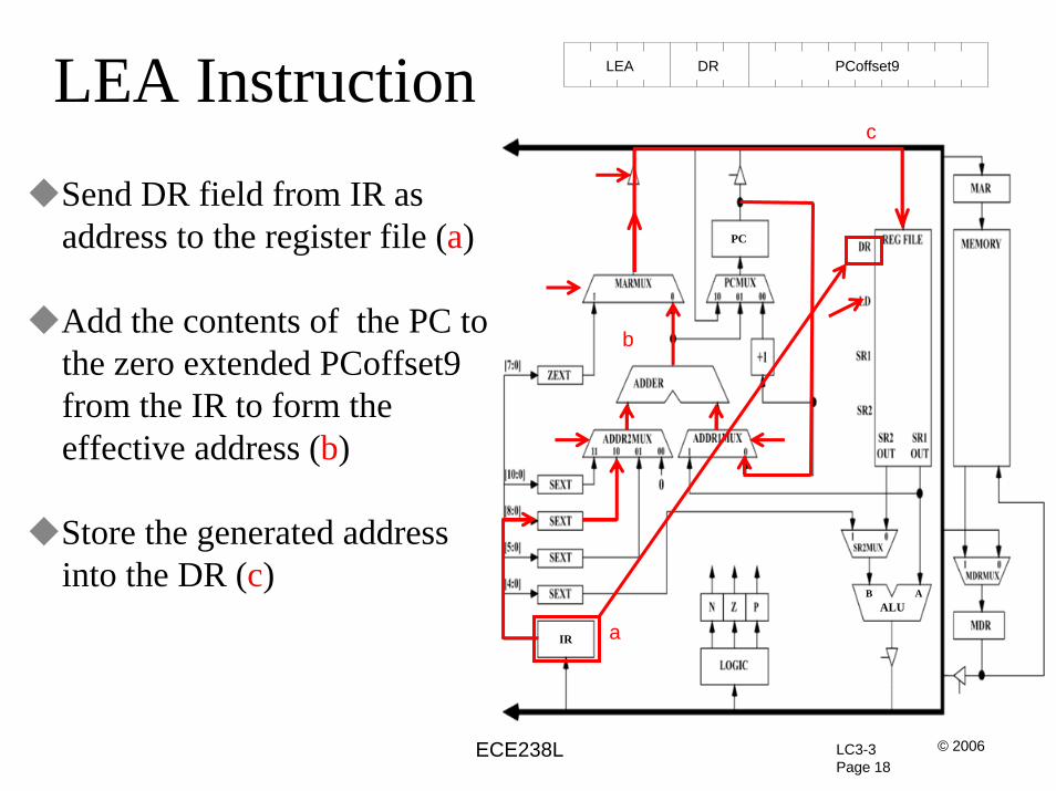
LEA InstructionSend DR field from IR as address to the register file (a)
Add the contents of the PC tothe zero extended PCoffset9from the IR to form the effective address (b)
Store the generated address into the DR (c)
a
b
c
IR
ALU
PC
AB
LEA PCoffset9DR
LC3-3Page 19
© 2006ECE238L
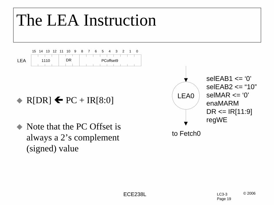
The LEA Instruction15 14 13 12 11 10 9 8 7 6 5 4 3 2 1 0
LEA 1110 PCoffset9DR
LEA0
selEAB1 <= ‘0’selEAB2 <= “10”selMAR <= ‘0’enaMARMDR <= IR[11:9] regWE
to Fetch0
R[DR] PC + IR[8:0]
Note that the PC Offset is always a 2’s complement (signed) value
LC3-3Page 20
© 2006ECE238L
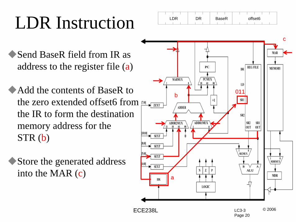
LDR Instruction LDR offset6DR BaseR
Send BaseR field from IR as address to the register file (a)
Add the contents of BaseR tothe zero extended offset6 fromthe IR to form the destinationmemory address for the STR (b)
Store the generated address into the MAR (c) a
011b
c
IR
ALU
PC
AB
LC3-3Page 21
© 2006ECE238L
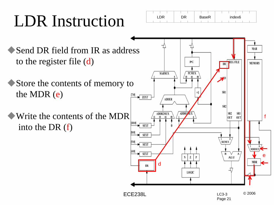
LDR Instruction LDR index6DR BaseR
Send DR field from IR as address to the register file (d)
Store the contents of memory tothe MDR (e)
Write the contents of the MDRinto the DR (f)
dIR
ALU
PC
e
f
AB
LC3-3Page 22
© 2006ECE238L
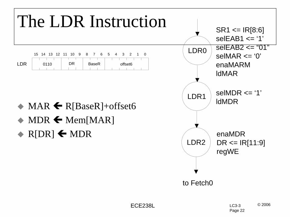
The LDR Instruction15 14 13 12 11 10 9 8 7 6 5 4 3 2 1 0
MAR R[BaseR]+offset6MDR Mem[MAR]R[DR] MDR
LDR0
SR1 <= IR[8:6]selEAB1 <= ‘1’selEAB2 <= “01”selMAR <= ‘0’enaMARMldMAR
LDR1
LDR2enaMDRDR <= IR[11:9]regWE
to Fetch0
LDR 0110 offset6DR BaseR
selMDR <= ‘1’ldMDR
LC3-3Page 23
© 2006ECE238L
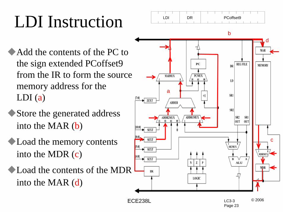
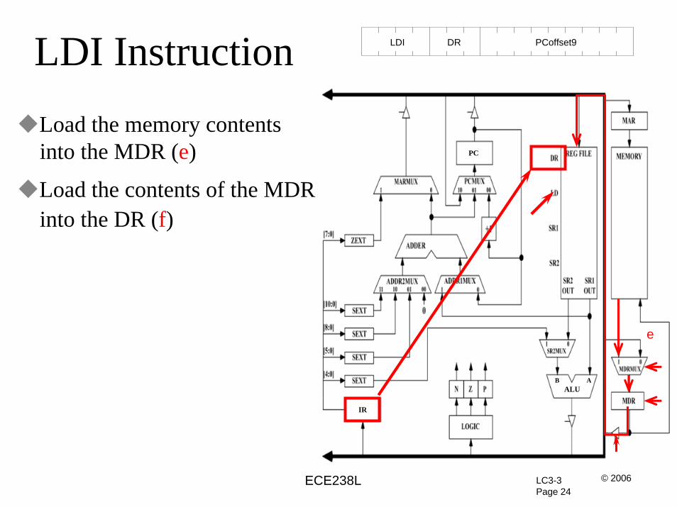
LDI Instruction LDI PCoffset9DR
Add the contents of the PC tothe sign extended PCoffset9 from the IR to form the sourcememory address for the LDI (a)
Store the generated address into the MAR (b)
Load the memory contents into the MDR (c)
Load the contents of the MDRinto the MAR (d)
a
IR
ALU
PC
AB
b
c
d
LC3-3Page 24
© 2006ECE238L
LDI Instruction LDI PCoffset9DR
Load the memory contents into the MDR (e)
Load the contents of the MDRinto the DR (f)
IR
ALU
PC
AB
e

LC3-3Page 25
© 2006ECE238L
The LDI Instruction15 14 13 12 11 10 9 8 7 6 5 4 3 2 1 0
MAR PC + IR[8:0]MDR Mem[MAR]MAR MDRMDR Mem[MAR]R[DR] MDR
LDI0
LDI1
LDI2 enaMDRldMAR
to Fetch0
LDI 1010 PCoffset9DR
LDI4
LDI3
enaMDRDR <= IR[11:9]regWE
selEAB1 <= ‘0’selEAB2 <= “10”selMAR <= ‘0’enaMARMldMAR
selMDR <= ‘1’ldMDR
selMDR <= ‘1’ldMDR

LC3-3Page 26
© 2006ECE238L
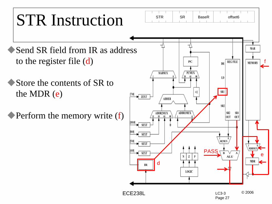
STR Instruction
Send BaseR field from IR as address to the register file (a)
Add the contents of BaseR tothe zero extended offset6 fromthe IR to form the destinationmemory address for the STR (b)
Store the generated address into the MAR (c) a
b
c
IR
ALU
PC
AB
STR offset6SR BaseR
LC3-3Page 27
© 2006ECE238L
STR Instruction STR offset6SR BaseR
Send SR field from IR as address to the register file (d)
Store the contents of SR tothe MDR (e)
Perform the memory write (f)
dIR
ALU
PC
PASS e
f
AB
LC3-3Page 28
© 2006ECE238L
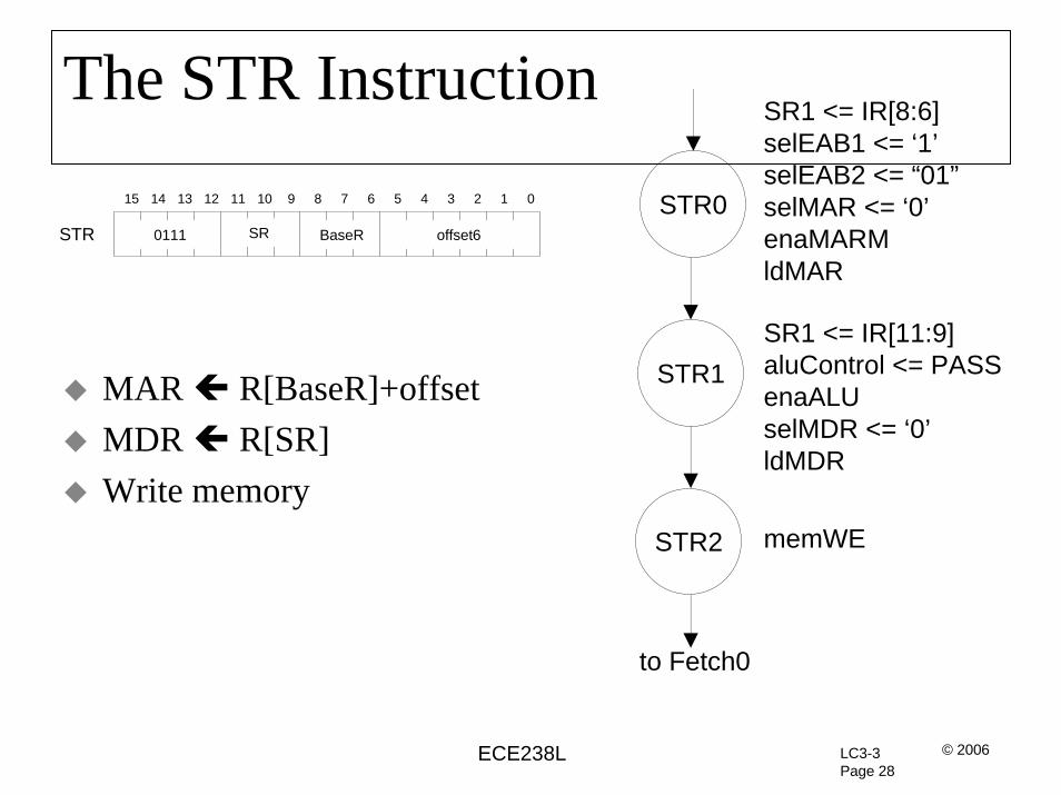
The STR Instruction15 14 13 12 11 10 9 8 7 6 5 4 3 2 1 0
MAR R[BaseR]+offsetMDR R[SR]Write memory
STR0
SR1 <= IR[8:6]selEAB1 <= ‘1’selEAB2 <= “01”selMAR <= ‘0’enaMARMldMAR
STR1
STR2 memWE
SR1 <= IR[11:9]aluControl <= PASSenaALUselMDR <= ‘0’ldMDR
to Fetch0
STR 0111 offset6SR BaseR
LC3-3Page 29
© 2006ECE238L
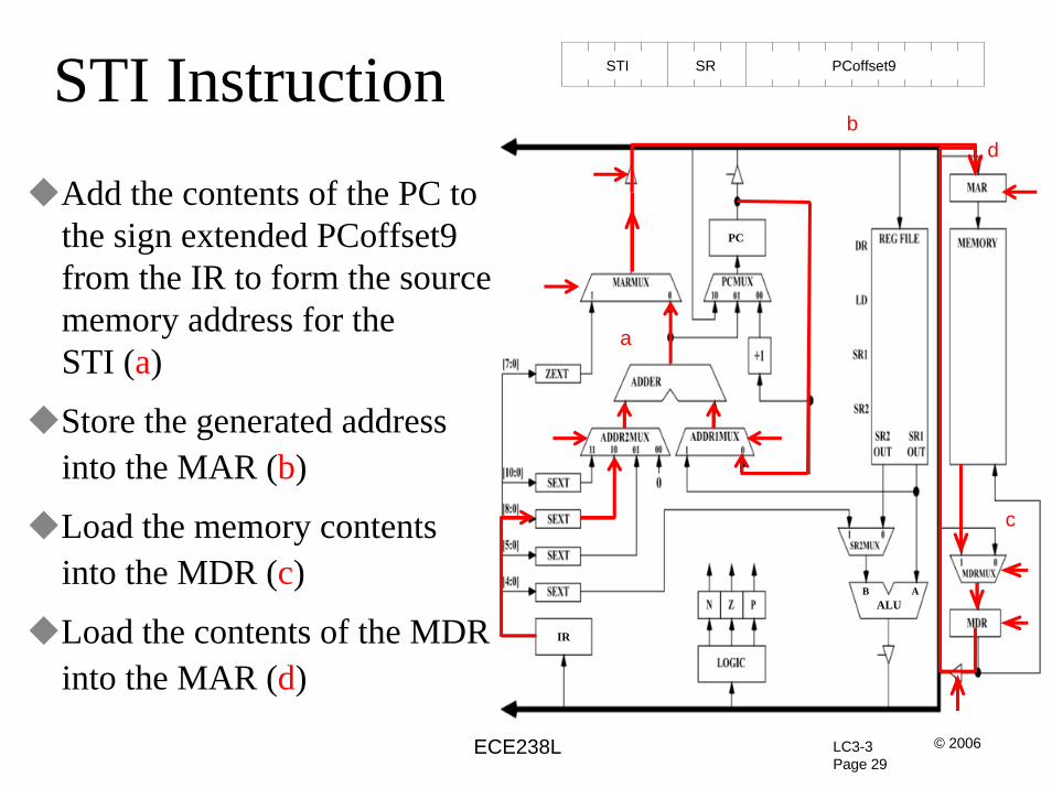
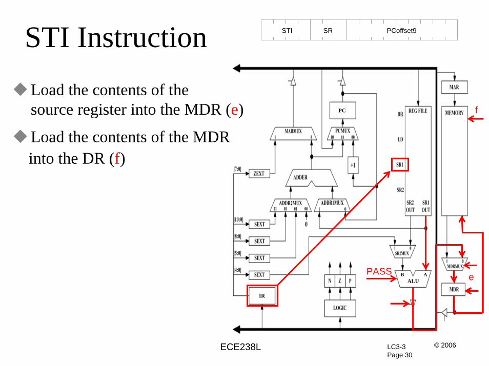
STI Instruction STI PCoffset9SR
Add the contents of the PC tothe sign extended PCoffset9 from the IR to form the sourcememory address for the STI (a)
Store the generated address into the MAR (b)
Load the memory contents into the MDR (c)
Load the contents of the MDRinto the MAR (d)
a
IR
ALU
PC
AB
b
c
d
LC3-3Page 30
© 2006ECE238L
STI Instruction STI PCoffset9SR
Load the contents of the source register into the MDR (e)
Load the contents of the MDRinto the DR (f)
IR
ALU
PC
ABPASS e
f
LC3-3Page 31
© 2006ECE238L
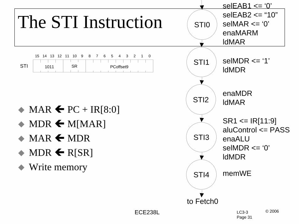
The STI Instruction15 14 13 12 11 10 9 8 7 6 5 4 3 2 1 0
enaMDRldMAR
MAR PC + IR[8:0]MDR M[MAR]MAR MDRMDR R[SR]Write memory
STI 1011 PCoffset9SR
SR1 <= IR[11:9]aluControl <= PASSenaALUselMDR <= ‘0’ldMDR
memWE
selEAB1 <= ‘0’selEAB2 <= “10”selMAR <= ‘0’enaMARMldMAR
selMDR <= ‘1’ldMDR
STI0
STI1
STI2
to Fetch0
STI4
STI3
LC3-3Page 32
© 2006ECE238L
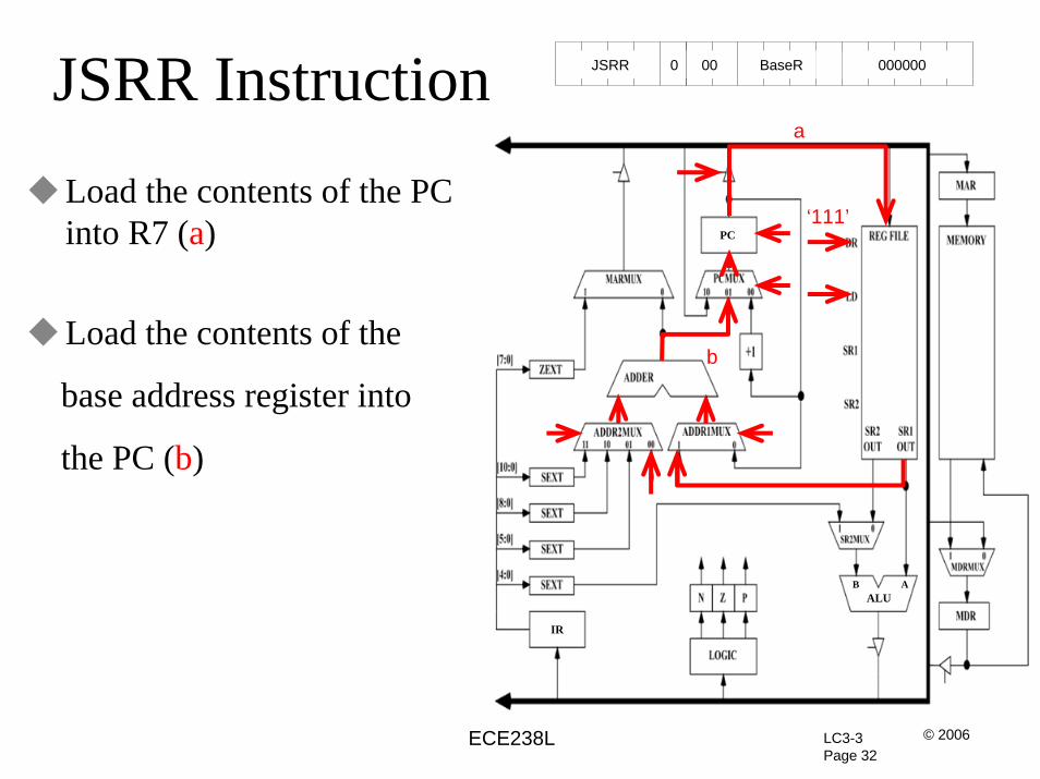
JSRR Instruction JSRR 00000000
Load the contents of the PC into R7 (a)
Load the contents of the
base address register into
the PC (b)
IR
ALU
PC
AB
0 BaseR
‘111’
a
b
LC3-3Page 33
© 2006ECE238L
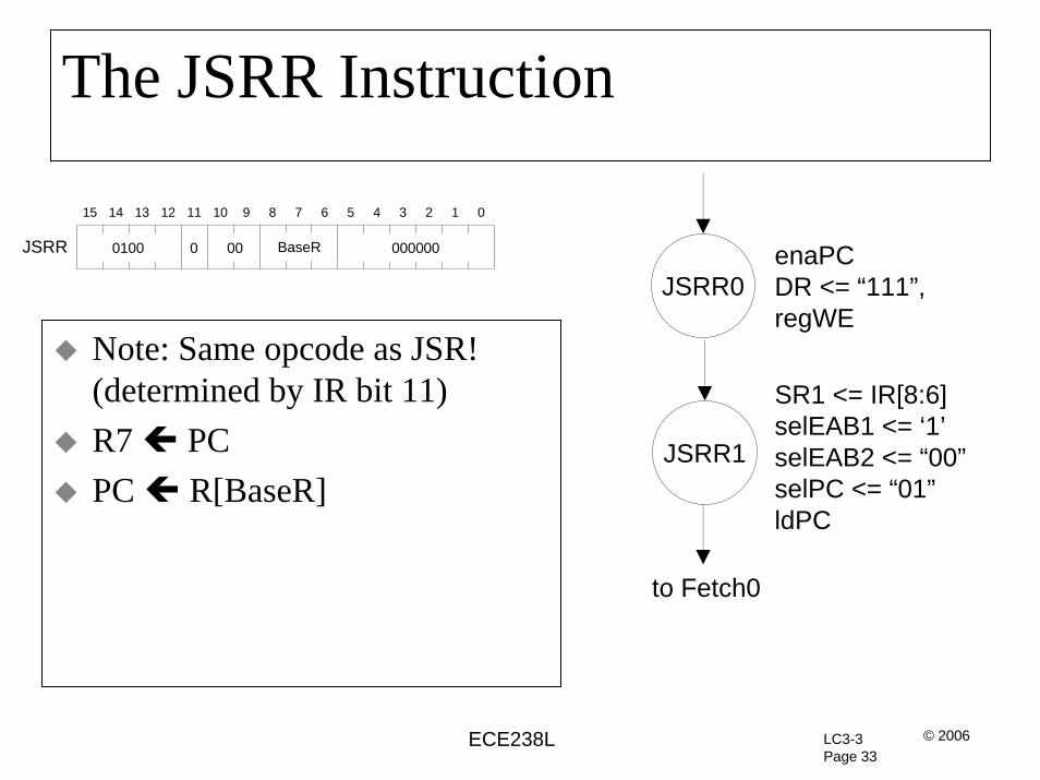
The JSRR Instruction
Note: Same opcode as JSR! (determined by IR bit 11)R7 PCPC R[BaseR]
15 14 13 12 11 10 9 8 7 6 5 4 3 2 1 0
enaPCDR <= “111”,regWE
JSRR 0100 0 00000000 BaseR
SR1 <= IR[8:6]selEAB1 <= ‘1’selEAB2 <= “00”selPC <= “01”ldPC
JSRR1
to Fetch0
JSRR0

LC3-3Page 34
© 2006ECE238L
The BR Instruction
Simply check NZP flags with nzp from instruction to decide whether to ldPC or notMethod 1: Could bring nzp flags into FSM as inputs and put comparison into state table… Bad idea
Method 2: Do comparison with some external gates and bring single-bit input into FSM….Good idea
BR 0000 n z p PCoffset9
15 14 13 12 11 10 9 8 7 6 5 4 3 2 1 0
LC3-3Page 35
© 2006ECE238L
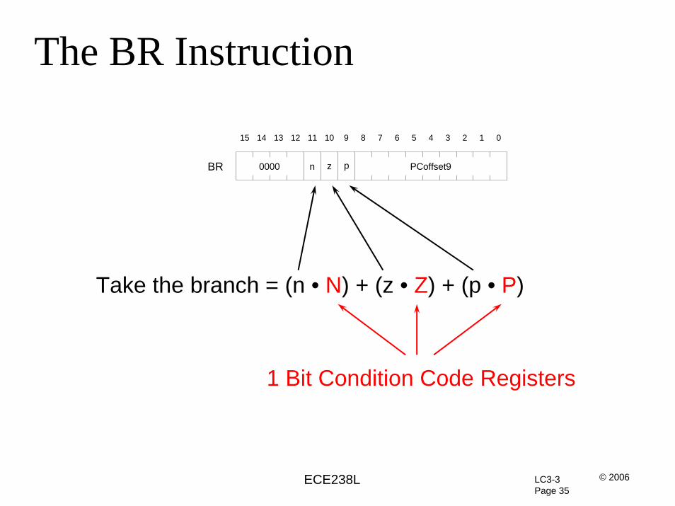
The BR Instruction
BR 0000 n z p PCoffset9
15 14 13 12 11 10 9 8 7 6 5 4 3 2 1 0
Take the branch = (n • N) + (z • Z) + (p • P)
1 Bit Condition Code Registers