Embed Size (px)
Citation preview
Layout Decomposition of Self-Aligned Double Patterning for2D Random Logic Patterning
Yongchan Ban†, Alex Miloslavsky‡, Kevin Lucas‡,Soo-Han Choi§, Chul-Hong Park§, and David Z. Pan†
†The University of Texas, Austin, TX, USA‡Synopsys Inc., Austin, TX, USA
§Samsung Electronics, Hwasung, South Korea
ABSTRACT
Self-aligned double pattering (SADP) has been adapted as a promising solution for sub-30nm technology nodesdue to its lower overlay problem and better process tolerance. SADP is in production use for 1D dense patternswith good pitch control such as NAND Flash memory applications, but it is still challenging to apply SADP to2D random logic patterns. The favored type of SADP for complex logic interconnects is a two mask approachusing a core mask and a trim mask. In this paper, we first describe layout decomposition methods of spacer-type double patterning lithography, then report a type of SADP compliant layouts, and finally report SADPapplications on Samsung 22nm SRAM layout. For SADP decomposition, we propose several SADP-aware layoutcoloring algorithms and a method of generating lithography-friendly core mask patterns. Experimental resultson 22nm node designs show that our proposed layout decomposition for SADP effectively decomposes any givenlayouts.
Keywords: Double patterning, SADP, decomposition, lithography, random logic patterning, sub-30nm
1. INTRODUCTION
SADP is a pitch-splitting sidewall image method that also utilizes two masks: a core mask and a trim mask.The core mask defines core mandrel patterns, and the sidewall spacer is deposited onto all sides of a mandrelpattern to enable pitch doubling in the patterning. The trim mask removes unnecessary patterns by blockingor unblocking with photoresist (PR). Since the most critical patterning control in SADP is not governed bylithography, but by the deposition of the sidewall spacer, it guarantees less overlay requirements and excellentvariability control compared to LELE DPT [1–5].
However, SADP allows only a single width of sidewall spacer which forms either a single wire width or a singlewire space. Therefore, SADP was previously limited by the lack of flexibility in terms of layout decomposition.Thus, SADP is in production use for 1D patterns in NAND Flash memory applications but applying SADP to 2Drandom logic patterns is challenging [5–7]. Due to its limitation, SADP might require three masks for 2D-typeapplication. However, since the manufacturing cost of logic products is dominated by the mask cost, a two-maskSADP approach is necessary for successful product application. Thus, layout decomposition for random 2D-typecomplex logic features which have various wire width and space is a primary challenging issue for a two-maskSADP process.
In this paper, we propose rigorous layout decomposition methods on SADP technique for sub-30nm randomshaped logic metal layouts. This paper describes methods for automatically choosing and optimizing the manu-facturability of base core mask patterns, generating assist core patterns, and optimizing trim mask patterns inSADP process. The major contributions of this paper include the following:
Further author information:Yongchan (James) Ban: [email protected], +1-512-906-8692Alex Miloslavsky: [email protected] Lucas: [email protected] Choi: [email protected] Park: [email protected] Z. Pan: [email protected]
Design for Manufacturability through Design-Process Integration V, edited by Michael L. Rieger, Mark. E. Mason, Proc. of SPIE Vol. 7974, 79740L · © 2011 SPIE · CCC code: 0277-786X/11/$18 · doi: 10.1117/12.879500
Proc. of SPIE Vol. 7974 79740L-1
Downloaded From: http://proceedings.spiedigitallibrary.org/ on 05/21/2014 Terms of Use: http://spiedl.org/terms
• Methods of SADP mask decomposition with a two-mask approach for random 2D-type logic features areproposed. Base core mask patterns are made up of main core patterns which are chosen from the originallayout using our SADP-aware layout coloring and of assist core patterns which can be generated in alithography friendly manner.
• The layout coloring highly affects the manufacturability of the core mask and trim mask layout. To resolvemanufacturing conflict on the core mask layout, we propose a grouping and merging algorithm. Meanwhile,we propose a trim mask friendly coloring incorporated with shortest-path coloring which can produce thebest coloring layout for the trim mask layout.
• We evaluate our technique on 22nm node industrial standard cells and SRAM logic designs. By introducinglayout retargeting we can achieve a feasible SADP decomposition for random 2D design which shows variousspaces and widths
The rest of the paper is organized as follows. Section 2 describes SADP lithography process and the chal-lenging issues. Section 3 presents several layout coloring approaches for DRC-free decomposed mast layoutsand algorithms of the core mask generation. A type of SADP compliant layouts is presented in Section 4.Experimental results are discussed in Section 5, followed by conclusions in Section 6.
2. SPACER-TYPE DOUBLE PATTERNING
We first summarize some terminologies and notations which are used throughout this paper:
• Core mask : the first mask in the SADP process flow.
• Mandrel : the printed patterns generated by the core mask where the sidewall spacers are subsequentlyformed.
• Main mandrel : the base mandrel layout which is a chosen subset of the design intent.
• Additional mandrel : the extra mandrel layout whose features need to be newly generated.
• Secondary metal : the layout except the main mandrel in the original layout. It is generated by merging ofspacer patterns of mandrel layouts.
(1) Target
(2) Core 1st lithography & Etch shrink
(3) Sidewall deposition
(5) Trim block 2nd lithography
(6) Etch of sub-layers
(4) Removing Core
(a) SIM-type SADP
(1) Target
(2) Core 1st lithography & Etch shrink
(3) Sidewall deposition
(5) Trim 2nd lithography
(6) Spacer removal & Etch
(4) Removing Core & BARC depo.
(b) SID-type SADP
Figure 1. Two types of self-aligned double pattering
Proc. of SPIE Vol. 7974 79740L-2
Downloaded From: http://proceedings.spiedigitallibrary.org/ on 05/21/2014 Terms of Use: http://spiedl.org/terms
• Spacer : the sidewall spacer, which is deposited on the mandrel layout, is formed at the both sides ofmandrels.
• Trim mask : the second mask in the SADP process flow and for removing away unnecessary segments ofmetals.
Two types of SADP process are popularly used for the state-of-the-art lithography patterning: SIM-typeSADP and SID-type SADP. Figure 1 shows the vertical view of SADP process sequences for SIM (a) and SID(b) type SADP. SIM is an abbreviation of “spacer is metal” where the sidewall spacer itself becomes the finalmetal patterns. Core layout, which is called as mandrel layout and becomes the first mask layout in SADP, isdesigned based on the space region between metal lines as in (a)-(2). Then, the side-wall spacers are generatedbased on the core mandrel layout in (a)-(3). After removing mandrels in (a)-(4) and processing the secondmask trimming step in (a)-(5), the final dense features are patterned on wafer matched with the design intentin (a)-(6).
The other type of SADP is SID which is an acronym of “spacer is dielectric”. The steps are similar toSIM, but, in SID-type SADP the side-wall spacer is just dielectric. Meanwhile, the mandrel layout becomesfinal metal patterns. The base mandrel layout is chosen from the original layout as shown in Figure 1(b)-(2).Then, the sidewall spacers are generated nearby the mandrel layout in (b)-(3). After removing mandrels, wedeposit substrate materials in (b)-(4). Then, the second trimming mask is used for getting the final patternsin (b)-(5)&(6). Since the base mandrel layout is a subset of the original layout and should have enough layoutpitch for the 1st lithography patterning, it is usually chosen from the layout coloring [4, 5].
Since the width of the sidewall spacer is constant, it is hard to vary the pattern line-width in SIM-typeSADP because the sidewall spacer becomes the metal line. Whereas, in SID-type SADP it is hard to control thepattern space because the side wall spacer becomes a space between two Mandrel metal patterns in SID. Sincethe core mandrel layout in SID-type SADP becomes the final metal pattern, SID-type SADP enables variousmetal widths. Moreover, as SID-type SADP has fewer process steps than SIM-type SADP, it provides more costeffective metal patterning [5, 7].
Let us look at SID-type SADP sequences in a way of top view in Figure 2. The layout coloring is first doneto select the base mandrel from the original target in (2). Either color between two colored layouts can be thebase mandrel in our approach. Then, extra mandrel layouts are added on the base mandrel to eventually makepatterns which are not chosen to the base mandrel. Note that the fist core mask is usually biased and bigger thanthe design intent for better lithography printability in (3). After decreasing the first mandrel pattern as much
(1) target design (3) mandrel design
& 1st litho mask
Mai
n M
andr
el
Add
ition
al
(7) BARC deposition (8) 2nd litho trim mask(9) final patterning
= Trim NOT Spacer
(2) layout coloring
Mai
n M
andr
el
Add
ition
al
(4) etch shrink
Mai
n M
andr
el
Add
ition
al
(5) sidewall deposition
(6) remove mandrels
Figure 2. The top view of SID-type SADP process
Proc. of SPIE Vol. 7974 79740L-3
Downloaded From: http://proceedings.spiedigitallibrary.org/ on 05/21/2014 Terms of Use: http://spiedl.org/terms
as the target size in (4), the sidewall spacers are formed around the mandrel as in (5). After removing mandrelsin (6) and depositing the substrate material, e.g., BARC in (7), we remove out the unnecessary polygons exceptthe design intent with the trim mask in (8).
Note that since the spacer patterns nearby mandrels will be etched out after the trim mask patterning, thespacer acts like a layout separator among the main mandrel and the secondary metal line. It implies that if theedge of a trim mask layout is on the spacer region, the trim layout can be free from mask overlay variationswithout any impact on target metal lines. In the other words, we should carefully control the mask overlay ifthe trim mask edge is on metal lines.
There are many challenges involved with creating a core mandrel mask and a trim mask for complex 2Dlayouts. In particular, layout coloring and assist mandrel generation are utmost important steps in an SADPmask synthesis process: layout coloring and additional mandrel generation. The manufacturability on both thecore mask and trim mask is significantly dependant on layout coloring which, therefore, is one of crucial steps inSADP mask decomposition. The trim mask provides additional flexibility for patterning 2D patterns on wafer.Layout coloring is more highly affects on the lithographic printability of the second trim mask rather than thecore mask. We will discuss it in Section 3.1 and 3.2. It requires an intelligently designed mandrel layouts as agood starting point. The assist mandrel will provide the shapes of the secondary metal pattern, and it highlyaffects the lithographic printability of the fist core mask. Let us see the detail in Section 3.3.
3. MODELING OF MASK DECOMPOSITION FOR SADP
3.1. Grouping and Merging Coloring
Since SADP mask decomposition does not allow stitch insertion, some coloring conflict is usual. As shown inFigure 3, the target design has a native coloring conflict which represents an undecomposable layout even inLELE [1, 8]. To resolve this coloring conflict, we introduce a grouping and merging algorithm [9]. Once twosame colored polygons are within the minimum coloring distance d, we make a group for the polygons and mergethem into one polygon. By merging the two conflicted polygons, we can make a core mask without any DRCand lithography violations. This merged region between two grouped polygons should be trimmed out at the2nd trim mask patterning step. Note that since the spacer patterns nearby mandrels will become dielectric afterthe trim mask patterning, the spacer acts like an overlay-free region. It implies that if the edge of a trim masklayout is on the spacer region, the trim layout can be free from mask overlay variations without any impact ontarget metal lines. In the other words, we should carefully control the mask overlay if the trim mask edge is onmetal lines. Thus, we should note the following issues if a trim mask should cut the merged area:
• The width/space of a trim mask should meet the trim mask width constraint which is usually the same asthe minimum target layout width/space or slightly larger.
• Since the edge of a trim mask layout is passing over the main mandrel not the safe spacer region, theoverlay error of the trim mask should be carefully controlled.
A B
CD E
(a) coloring conflict
A DB
C
E
A DF E
(b) grouping
EF
(c) merging & core (d) spacer generation (e) trim cutting
Figure 3. Grouping and merging coloring
Proc. of SPIE Vol. 7974 79740L-4
Downloaded From: http://proceedings.spiedigitallibrary.org/ on 05/21/2014 Terms of Use: http://spiedl.org/terms
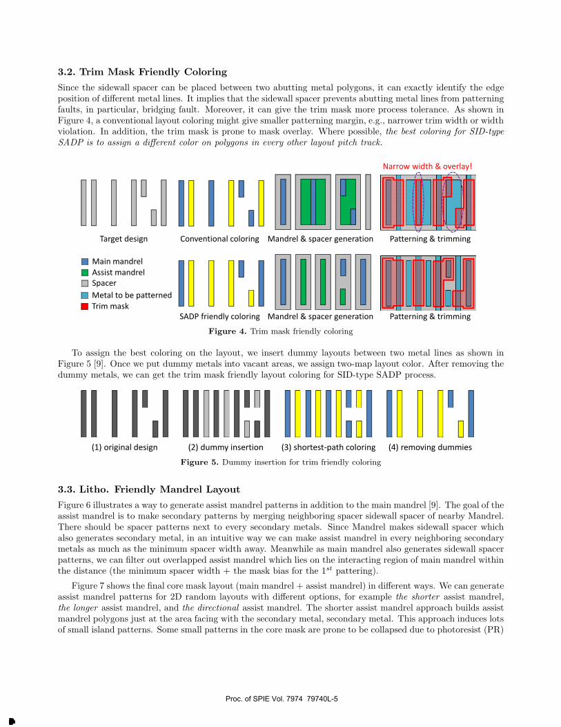
3.2. Trim Mask Friendly Coloring
Since the sidewall spacer can be placed between two abutting metal polygons, it can exactly identify the edgeposition of different metal lines. It implies that the sidewall spacer prevents abutting metal lines from patterningfaults, in particular, bridging fault. Moreover, it can give the trim mask more process tolerance. As shown inFigure 4, a conventional layout coloring might give smaller patterning margin, e.g., narrower trim width or widthviolation. In addition, the trim mask is prone to mask overlay. Where possible, the best coloring for SID-typeSADP is to assign a different color on polygons in every other layout pitch track.
Conventional coloring
SADP friendly coloring Mandrel & spacer generation Patterning & trimming
Main mandrel
Assist mandrel
Spacer
Metal to be patterned
Trim mask
Narrow width & overlay!
Mandrel & spacer generation Patterning & trimmingTarget design
Figure 4. Trim mask friendly coloring
To assign the best coloring on the layout, we insert dummy layouts between two metal lines as shown inFigure 5 [9]. Once we put dummy metals into vacant areas, we assign two-map layout color. After removing thedummy metals, we can get the trim mask friendly layout coloring for SID-type SADP process.
(1) original design (2) dummy insertion (3) shortest-path coloring (4) removing dummies
Figure 5. Dummy insertion for trim friendly coloring
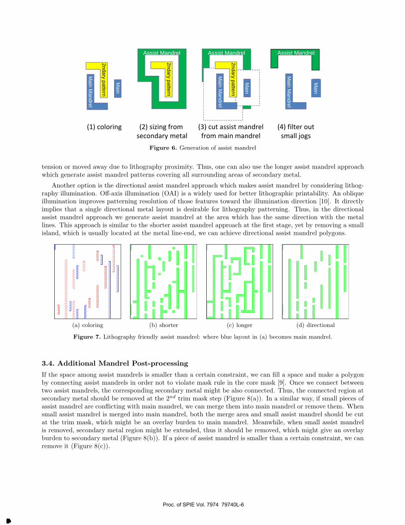
3.3. Litho. Friendly Mandrel Layout
Figure 6 illustrates a way to generate assist mandrel patterns in addition to the main mandrel [9]. The goal of theassist mandrel is to make secondary patterns by merging neighboring spacer sidewall spacer of nearby Mandrel.There should be spacer patterns next to every secondary metals. Since Mandrel makes sidewall spacer whichalso generates secondary metal, in an intuitive way we can make assist mandrel in every neighboring secondarymetals as much as the minimum spacer width away. Meanwhile as main mandrel also generates sidewall spacerpatterns, we can filter out overlapped assist mandrel which lies on the interacting region of main mandrel withinthe distance (the minimum spacer width + the mask bias for the 1st pattering).
Figure 7 shows the final core mask layout (main mandrel + assist mandrel) in different ways. We can generateassist mandrel patterns for 2D random layouts with different options, for example the shorter assist mandrel,the longer assist mandrel, and the directional assist mandrel. The shorter assist mandrel approach builds assistmandrel polygons just at the area facing with the secondary metal, secondary metal. This approach induces lotsof small island patterns. Some small patterns in the core mask are prone to be collapsed due to photoresist (PR)
Proc. of SPIE Vol. 7974 79740L-5
Downloaded From: http://proceedings.spiedigitallibrary.org/ on 05/21/2014 Terms of Use: http://spiedl.org/terms
Main M
andrel
2ndary pattern
Main
2ndary pattern
(1) coloring
2ndary pattern
Main M
andrel
Main
Main M
andrel
Main
Assist MandrelAssist MandrelAssist Mandrel
(2) sizing from
secondary metal
(3) cut assist mandrel
from main mandrel
(4) filter out
small jogs
Figure 6. Generation of assist mandrel
tension or moved away due to lithography proximity. Thus, one can also use the longer assist mandrel approachwhich generate assist mandrel patterns covering all surrounding areas of secondary metal.
Another option is the directional assist mandrel approach which makes assist mandrel by considering lithog-raphy illumination. Off-axis illumination (OAI) is a widely used for better lithographic printability. An obliqueillumination improves patterning resolution of those features toward the illumination direction [10]. It directlyimplies that a single directional metal layout is desirable for lithography patterning. Thus, in the directionalassist mandrel approach we generate assist mandrel at the area which has the same direction with the metallines. This approach is similar to the shorter assist mandrel approach at the first stage, yet by removing a smallisland, which is usually located at the metal line-end, we can achieve directional assist mandrel polygons.
(a) coloring (b) shorter (c) longer (d) directional
Figure 7. Lithography friendly assist mandrel: where blue layout in (a) becomes main mandrel.
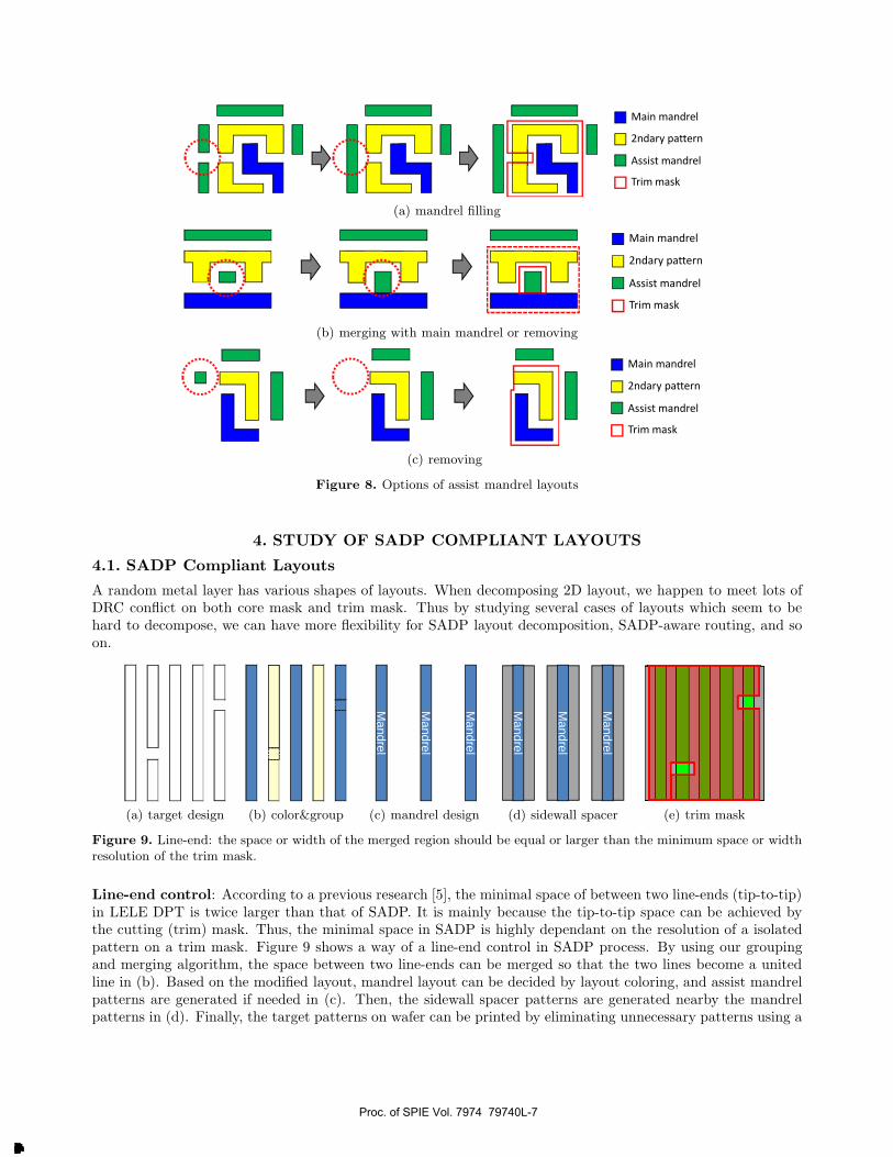
3.4. Additional Mandrel Post-processing
If the space among assist mandrels is smaller than a certain constraint, we can fill a space and make a polygonby connecting assist mandrels in order not to violate mask rule in the core mask [9]. Once we connect betweentwo assist mandrels, the corresponding secondary metal might be also connected. Thus, the connected region atsecondary metal should be removed at the 2nd trim mask step (Figure 8(a)). In a similar way, if small pieces ofassist mandrel are conflicting with main mandrel, we can merge them into main mandrel or remove them. Whensmall assist mandrel is merged into main mandrel, both the merge area and small assist mandrel should be cutat the trim mask, which might be an overlay burden to main mandrel. Meanwhile, when small assist mandrelis removed, secondary metal region might be extended, thus it should be removed, which might give an overlayburden to secondary metal (Figure 8(b)). If a piece of assist mandrel is smaller than a certain constraint, we canremove it (Figure 8(c)).
Proc. of SPIE Vol. 7974 79740L-6
Downloaded From: http://proceedings.spiedigitallibrary.org/ on 05/21/2014 Terms of Use: http://spiedl.org/terms
Main mandrel
2ndary pattern
Assist mandrel
Trim mask
(a) mandrel filling
Main mandrel
2ndary pattern
Assist mandrel
Trim mask
(b) merging with main mandrel or removing
Main mandrel
2ndary pattern
Assist mandrel
Trim mask
(c) removing
Figure 8. Options of assist mandrel layouts
4. STUDY OF SADP COMPLIANT LAYOUTS
4.1. SADP Compliant Layouts
A random metal layer has various shapes of layouts. When decomposing 2D layout, we happen to meet lots ofDRC conflict on both core mask and trim mask. Thus by studying several cases of layouts which seem to behard to decompose, we can have more flexibility for SADP layout decomposition, SADP-aware routing, and soon.
(a) target design (b) color&group
Mandrel
Mandrel
Mandrel
(c) mandrel design
Mandrel
Mandrel
Mandrel
(d) sidewall spacer (e) trim mask
Figure 9. Line-end: the space or width of the merged region should be equal or larger than the minimum space or widthresolution of the trim mask.
Line-end control: According to a previous research [5], the minimal space of between two line-ends (tip-to-tip)in LELE DPT is twice larger than that of SADP. It is mainly because the tip-to-tip space can be achieved bythe cutting (trim) mask. Thus, the minimal space in SADP is highly dependant on the resolution of a isolatedpattern on a trim mask. Figure 9 shows a way of a line-end control in SADP process. By using our groupingand merging algorithm, the space between two line-ends can be merged so that the two lines become a unitedline in (b). Based on the modified layout, mandrel layout can be decided by layout coloring, and assist mandrelpatterns are generated if needed in (c). Then, the sidewall spacer patterns are generated nearby the mandrelpatterns in (d). Finally, the target patterns on wafer can be printed by eliminating unnecessary patterns using a
Proc. of SPIE Vol. 7974 79740L-7
Downloaded From: http://proceedings.spiedigitallibrary.org/ on 05/21/2014 Terms of Use: http://spiedl.org/terms
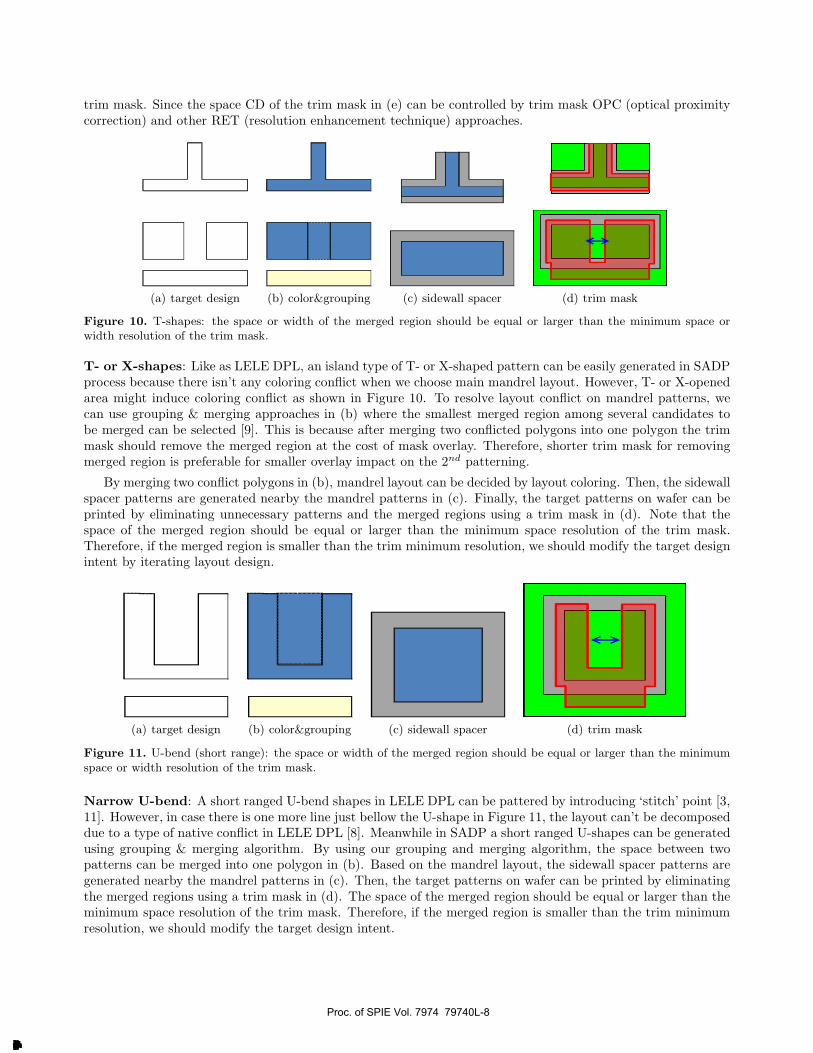
trim mask. Since the space CD of the trim mask in (e) can be controlled by trim mask OPC (optical proximitycorrection) and other RET (resolution enhancement technique) approaches.
(a) target design (b) color&grouping (c) sidewall spacer (d) trim mask
Figure 10. T-shapes: the space or width of the merged region should be equal or larger than the minimum space orwidth resolution of the trim mask.
T- or X-shapes: Like as LELE DPL, an island type of T- or X-shaped pattern can be easily generated in SADPprocess because there isn’t any coloring conflict when we choose main mandrel layout. However, T- or X-openedarea might induce coloring conflict as shown in Figure 10. To resolve layout conflict on mandrel patterns, wecan use grouping & merging approaches in (b) where the smallest merged region among several candidates tobe merged can be selected [9]. This is because after merging two conflicted polygons into one polygon the trimmask should remove the merged region at the cost of mask overlay. Therefore, shorter trim mask for removingmerged region is preferable for smaller overlay impact on the 2nd patterning.
By merging two conflict polygons in (b), mandrel layout can be decided by layout coloring. Then, the sidewallspacer patterns are generated nearby the mandrel patterns in (c). Finally, the target patterns on wafer can beprinted by eliminating unnecessary patterns and the merged regions using a trim mask in (d). Note that thespace of the merged region should be equal or larger than the minimum space resolution of the trim mask.Therefore, if the merged region is smaller than the trim minimum resolution, we should modify the target designintent by iterating layout design.
(a) target design (b) color&grouping (c) sidewall spacer (d) trim mask
Figure 11. U-bend (short range): the space or width of the merged region should be equal or larger than the minimumspace or width resolution of the trim mask.
Narrow U-bend: A short ranged U-bend shapes in LELE DPL can be pattered by introducing ‘stitch’ point [3,11]. However, in case there is one more line just bellow the U-shape in Figure 11, the layout can’t be decomposeddue to a type of native conflict in LELE DPL [8]. Meanwhile in SADP a short ranged U-shapes can be generatedusing grouping & merging algorithm. By using our grouping and merging algorithm, the space between twopatterns can be merged into one polygon in (b). Based on the mandrel layout, the sidewall spacer patterns aregenerated nearby the mandrel patterns in (c). Then, the target patterns on wafer can be printed by eliminatingthe merged regions using a trim mask in (d). The space of the merged region should be equal or larger than theminimum space resolution of the trim mask. Therefore, if the merged region is smaller than the trim minimumresolution, we should modify the target design intent.
Proc. of SPIE Vol. 7974 79740L-8
Downloaded From: http://proceedings.spiedigitallibrary.org/ on 05/21/2014 Terms of Use: http://spiedl.org/terms
(a) target design (b) color&grouping (c) sidewall spacer (d) trim mask
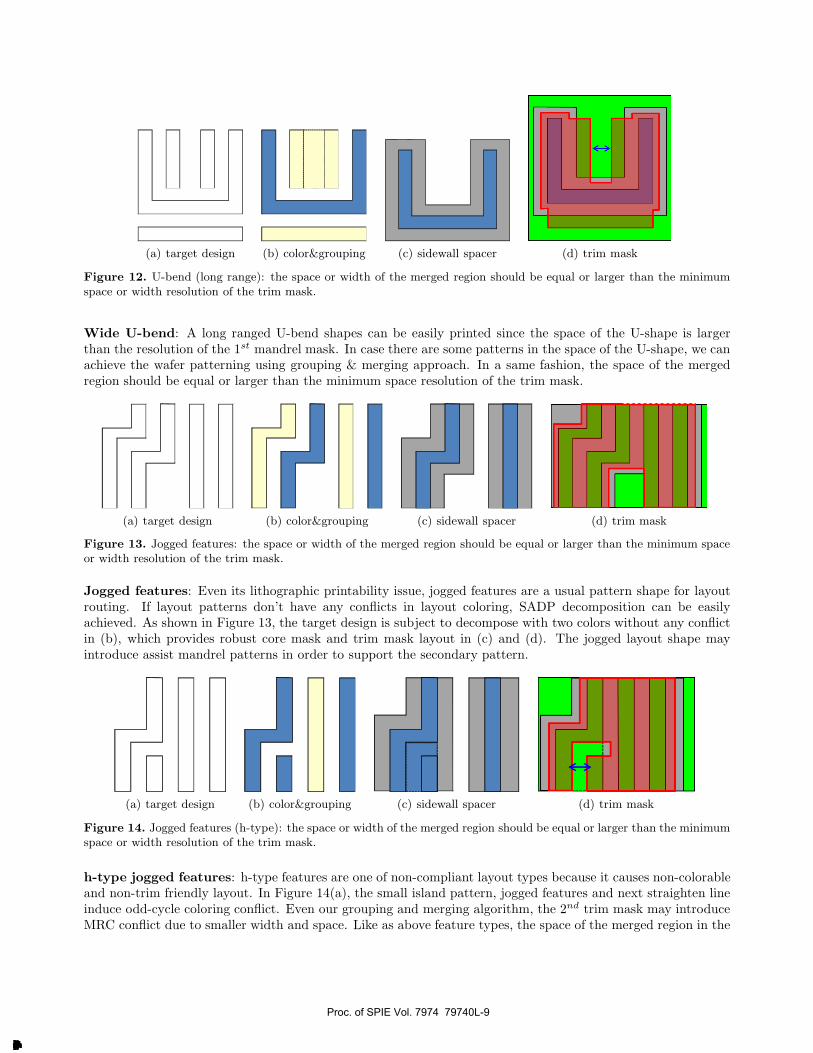
Figure 12. U-bend (long range): the space or width of the merged region should be equal or larger than the minimumspace or width resolution of the trim mask.
Wide U-bend: A long ranged U-bend shapes can be easily printed since the space of the U-shape is largerthan the resolution of the 1st mandrel mask. In case there are some patterns in the space of the U-shape, we canachieve the wafer patterning using grouping & merging approach. In a same fashion, the space of the mergedregion should be equal or larger than the minimum space resolution of the trim mask.
(a) target design (b) color&grouping (c) sidewall spacer (d) trim mask
Figure 13. Jogged features: the space or width of the merged region should be equal or larger than the minimum spaceor width resolution of the trim mask.
Jogged features: Even its lithographic printability issue, jogged features are a usual pattern shape for layoutrouting. If layout patterns don’t have any conflicts in layout coloring, SADP decomposition can be easilyachieved. As shown in Figure 13, the target design is subject to decompose with two colors without any conflictin (b), which provides robust core mask and trim mask layout in (c) and (d). The jogged layout shape mayintroduce assist mandrel patterns in order to support the secondary pattern.
(a) target design (b) color&grouping (c) sidewall spacer (d) trim mask
Figure 14. Jogged features (h-type): the space or width of the merged region should be equal or larger than the minimumspace or width resolution of the trim mask.
h-type jogged features: h-type features are one of non-compliant layout types because it causes non-colorableand non-trim friendly layout. In Figure 14(a), the small island pattern, jogged features and next straighten lineinduce odd-cycle coloring conflict. Even our grouping and merging algorithm, the 2nd trim mask may introduceMRC conflict due to smaller width and space. Like as above feature types, the space of the merged region in the
Proc. of SPIE Vol. 7974 79740L-9
Downloaded From: http://proceedings.spiedigitallibrary.org/ on 05/21/2014 Terms of Use: http://spiedl.org/terms
core mask should be equal or larger than the minimum space resolution of the trim mask.
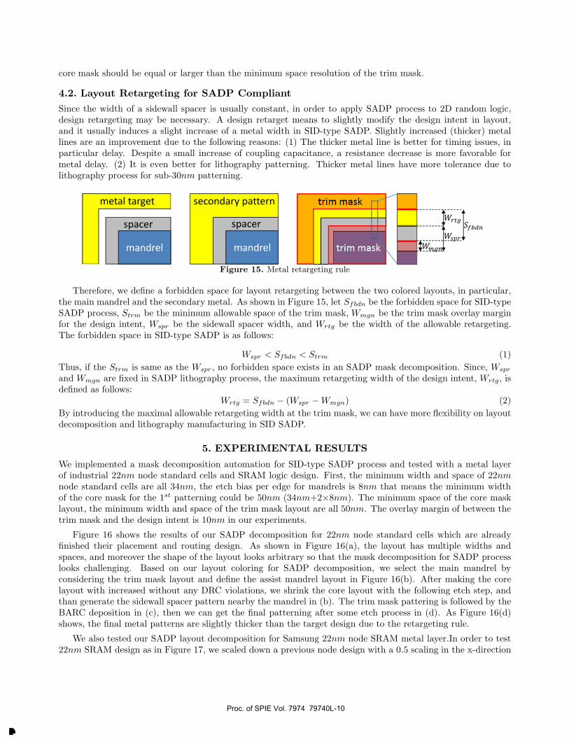
4.2. Layout Retargeting for SADP Compliant
Since the width of a sidewall spacer is usually constant, in order to apply SADP process to 2D random logic,design retargeting may be necessary. A design retarget means to slightly modify the design intent in layout,and it usually induces a slight increase of a metal width in SID-type SADP. Slightly increased (thicker) metallines are an improvement due to the following reasons: (1) The thicker metal line is better for timing issues, inparticular delay. Despite a small increase of coupling capacitance, a resistance decrease is more favorable formetal delay. (2) It is even better for lithography patterning. Thicker metal lines have more tolerance due tolithography process for sub-30nm patterning.
spacer
mandrel
metal target secondary pattern
spacer
mandrel
Figure 15. Metal retargeting rule
Therefore, we define a forbidden space for layout retargeting between the two colored layouts, in particular,the main mandrel and the secondary metal. As shown in Figure 15, let Sfbdn be the forbidden space for SID-typeSADP process, Strm be the minimum allowable space of the trim mask, Wmgn be the trim mask overlay marginfor the design intent, Wspr be the sidewall spacer width, and Wrtg be the width of the allowable retargeting.The forbidden space in SID-type SADP is as follows:
Wspr < Sfbdn < Strm (1)
Thus, if the Strm is same as the Wspr , no forbidden space exists in an SADP mask decomposition. Since, Wspr
and Wmgn are fixed in SADP lithography process, the maximum retargeting width of the design intent, Wrtg, isdefined as follows:
Wrtg = Sfbdn − (Wspr −Wmgn) (2)
By introducing the maximal allowable retargeting width at the trim mask, we can have more flexibility on layoutdecomposition and lithography manufacturing in SID SADP.
5. EXPERIMENTAL RESULTS
We implemented a mask decomposition automation for SID-type SADP process and tested with a metal layerof industrial 22nm node standard cells and SRAM logic design. First, the minimum width and space of 22nmnode standard cells are all 34nm, the etch bias per edge for mandrels is 8nm that means the minimum widthof the core mask for the 1st patterning could be 50nm (34nm+2×8nm). The minimum space of the core masklayout, the minimum width and space of the trim mask layout are all 50nm. The overlay margin of between thetrim mask and the design intent is 10nm in our experiments.
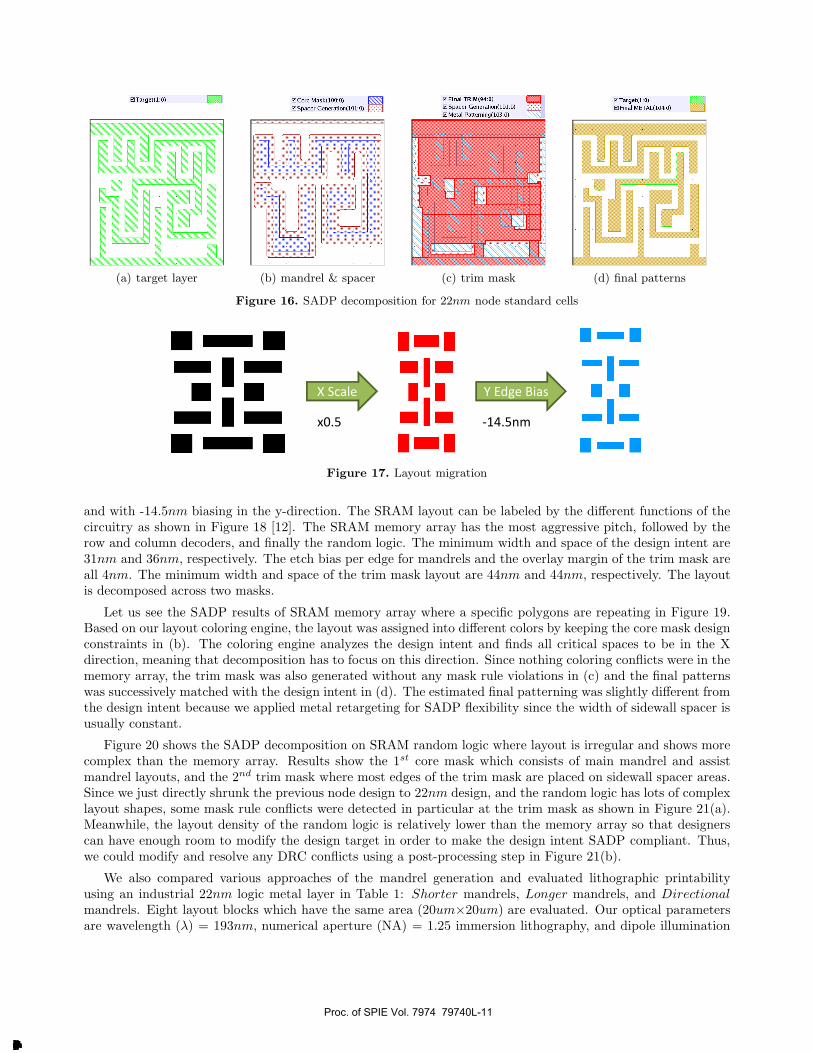
Figure 16 shows the results of our SADP decomposition for 22nm node standard cells which are alreadyfinished their placement and routing design. As shown in Figure 16(a), the layout has multiple widths andspaces, and moreover the shape of the layout looks arbitrary so that the mask decomposition for SADP processlooks challenging. Based on our layout coloring for SADP decomposition, we select the main mandrel byconsidering the trim mask layout and define the assist mandrel layout in Figure 16(b). After making the corelayout with increased without any DRC violations, we shrink the core layout with the following etch step, andthan generate the sidewall spacer pattern nearby the mandrel in (b). The trim mask pattering is followed by theBARC deposition in (c), then we can get the final patterning after some etch process in (d). As Figure 16(d)shows, the final metal patterns are slightly thicker than the target design due to the retargeting rule.
We also tested our SADP layout decomposition for Samsung 22nm node SRAM metal layer.In order to test22nm SRAM design as in Figure 17, we scaled down a previous node design with a 0.5 scaling in the x-direction
Proc. of SPIE Vol. 7974 79740L-10
Downloaded From: http://proceedings.spiedigitallibrary.org/ on 05/21/2014 Terms of Use: http://spiedl.org/terms
II
(a) target layer (b) mandrel & spacer (c) trim mask (d) final patterns
Figure 16. SADP decomposition for 22nm node standard cells
Y Edge Bias
-14.5nm
X Scale
x0.5
Figure 17. Layout migration
and with -14.5nm biasing in the y-direction. The SRAM layout can be labeled by the different functions of thecircuitry as shown in Figure 18 [12]. The SRAM memory array has the most aggressive pitch, followed by therow and column decoders, and finally the random logic. The minimum width and space of the design intent are31nm and 36nm, respectively. The etch bias per edge for mandrels and the overlay margin of the trim mask areall 4nm. The minimum width and space of the trim mask layout are 44nm and 44nm, respectively. The layoutis decomposed across two masks.
Let us see the SADP results of SRAM memory array where a specific polygons are repeating in Figure 19.Based on our layout coloring engine, the layout was assigned into different colors by keeping the core mask designconstraints in (b). The coloring engine analyzes the design intent and finds all critical spaces to be in the Xdirection, meaning that decomposition has to focus on this direction. Since nothing coloring conflicts were in thememory array, the trim mask was also generated without any mask rule violations in (c) and the final patternswas successively matched with the design intent in (d). The estimated final patterning was slightly different fromthe design intent because we applied metal retargeting for SADP flexibility since the width of sidewall spacer isusually constant.
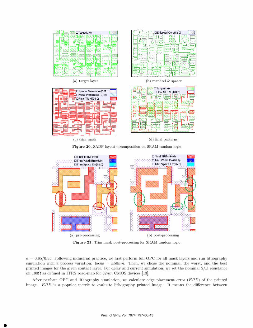
Figure 20 shows the SADP decomposition on SRAM random logic where layout is irregular and shows morecomplex than the memory array. Results show the 1st core mask which consists of main mandrel and assistmandrel layouts, and the 2nd trim mask where most edges of the trim mask are placed on sidewall spacer areas.Since we just directly shrunk the previous node design to 22nm design, and the random logic has lots of complexlayout shapes, some mask rule conflicts were detected in particular at the trim mask as shown in Figure 21(a).Meanwhile, the layout density of the random logic is relatively lower than the memory array so that designerscan have enough room to modify the design target in order to make the design intent SADP compliant. Thus,we could modify and resolve any DRC conflicts using a post-processing step in Figure 21(b).
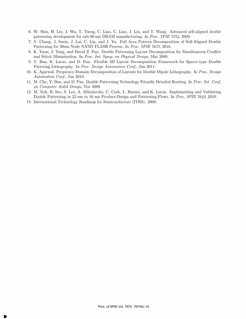
We also compared various approaches of the mandrel generation and evaluated lithographic printabilityusing an industrial 22nm logic metal layer in Table 1: Shorter mandrels, Longer mandrels, and Directionalmandrels. Eight layout blocks which have the same area (20um×20um) are evaluated. Our optical parametersare wavelength (λ) = 193nm, numerical aperture (NA) = 1.25 immersion lithography, and dipole illumination
Proc. of SPIE Vol. 7974 79740L-11
Downloaded From: http://proceedings.spiedigitallibrary.org/ on 05/21/2014 Terms of Use: http://spiedl.org/terms
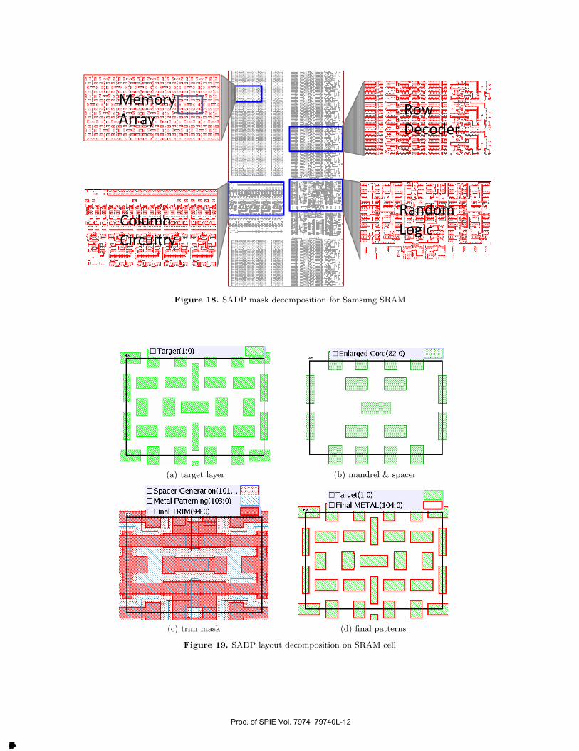
Memory
ArrayRow
Decoder
Random
LogicColumn
Circuitry
Figure 18. SADP mask decomposition for Samsung SRAM
(a) target layer (b) mandrel & spacer
(c) trim mask (d) final patterns
Figure 19. SADP layout decomposition on SRAM cell
Proc. of SPIE Vol. 7974 79740L-12
Downloaded From: http://proceedings.spiedigitallibrary.org/ on 05/21/2014 Terms of Use: http://spiedl.org/terms
(a) target layer (b) mandrel & spacer
(c) trim mask
100
(d) final patterns
Figure 20. SADP layout decomposition on SRAM random logic
(a) pre-processing (b) post-processing
Figure 21. Trim mask post-processing for SRAM random logic
σ = 0.85/0.55. Following industrial practice, we first perform full OPC for all mask layers and run lithographysimulation with a process variation: focus = ±50nm. Then, we chose the nominal, the worst, and the bestprinted images for the given contact layer. For delay and current simulation, we set the nominal S/D resistanceon 100Ω as defined in ITRS road-map for 32nm CMOS devices [13].
After perform OPC and lithography simulation, we calculate edge placement error (EPE) of the printedimage. EPE is a popular metric to evaluate lithography printed image. It means the difference between
Proc. of SPIE Vol. 7974 79740L-13
Downloaded From: http://proceedings.spiedigitallibrary.org/ on 05/21/2014 Terms of Use: http://spiedl.org/terms
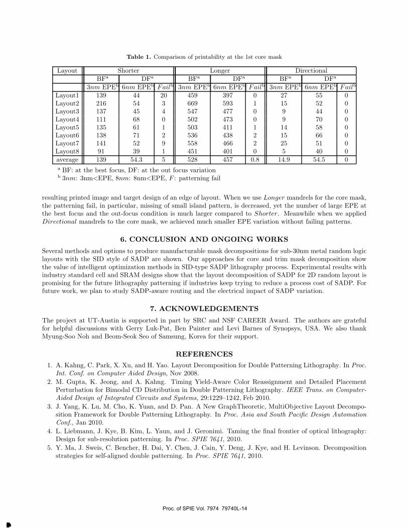
Table 1. Comparison of printability at the 1st core mask
Layout Shorter Longer DirectionalBFa DFa BFa DFa BFa DFa
3nm EPEb 6nm EPEb Failb 3nm EPEb 6nm EPEb Failb 3nm EPEb 6nm EPEb Failb
Layout1 139 44 20 459 397 0 27 55 0Layout2 216 54 3 669 593 1 15 52 0Layout3 137 45 4 547 477 0 9 44 0Layout4 111 68 0 502 473 0 9 70 0Layout5 135 61 1 503 411 1 14 58 0Layout6 138 71 2 536 438 2 15 66 0Layout7 141 52 9 558 466 2 25 51 0Layout8 91 39 1 451 401 0 5 40 0average 139 54.3 5 528 457 0.8 14.9 54.5 0a BF: at the best focus, DF: at the out focus variationb 3nm: 3nm<EPE, 8nm: 8nm<EPE, F : patterning fail
resulting printed image and target design of an edge of layout. When we use Longer mandrels for the core mask,the patterning fail, in particular, missing of small island pattern, is decreased, yet the number of large EPE atthe best focus and the out-focus condition is much larger compared to Shorter. Meanwhile when we appliedDirectional mandrels to the core mask, we achieved much smaller EPE variation without failing patterns.
6. CONCLUSION AND ONGOING WORKS
Several methods and options to produce manufacturable mask decompositions for sub-30nm metal random logiclayouts with the SID style of SADP are shown. Our approaches for core and trim mask decomposition showthe value of intelligent optimization methods in SID-type SADP lithography process. Experimental results withindustry standard cell and SRAM designs show that the layout decomposition of SADP for 2D random layout ispromising for the future lithography patterning if industries keep trying to reduce a process cost of SADP. Forfuture work, we plan to study SADP-aware routing and the electrical impact of SADP variation.
7. ACKNOWLEDGEMENTS
The project at UT-Austin is supported in part by SRC and NSF CAREER Award. The authors are gratefulfor helpful discussions with Gerry Luk-Pat, Ben Painter and Levi Barnes of Synopsys, USA. We also thankMyung-Soo Noh and Beom-Seok Seo of Samsung, Korea for their support.
REFERENCES
1. A. Kahng, C. Park, X. Xu, and H. Yao. Layout Decomposition for Double Patterning Lithography. In Proc.Int. Conf. on Computer Aided Design, Nov 2008.
2. M. Gupta, K. Jeong, and A. Kahng. Timing Yield-Aware Color Reassignment and Detailed PlacementPerturbation for Bimodal CD Distribution in Double Patterning Lithography. IEEE Trans. on Computer-Aided Design of Integrated Circuits and Systems, 29:1229–1242, Feb 2010.
3. J. Yang, K. Lu, M. Cho, K. Yuan, and D. Pan. A New GraphTheoretic, MultiObjective Layout Decompo-sition Framework for Double Patterning Lithography. In Proc. Asia and South Pacific Design AutomationConf., Jan 2010.
4. L. Liebmann, J. Kye, B. Kim, L. Yaun, and J. Geronimi. Taming the final frontier of optical lithography:Design for sub-resolution patterning. In Proc. SPIE 7641, 2010.
5. Y. Ma, J. Sweis, C. Bencher, H. Dai, Y. Chen, J. Cain, Y. Deng, J. Kye, and H. Levinson. Decompositionstrategies for self-aligned double patterning. In Proc. SPIE 7641, 2010.
Proc. of SPIE Vol. 7974 79740L-14
Downloaded From: http://proceedings.spiedigitallibrary.org/ on 05/21/2014 Terms of Use: http://spiedl.org/terms
6. W. Shiu, H. Liu, J. Wu, T. Tseng, C. Liao, C. Liao, J. Liu, and T. Wang. Advanced self-aligned doublepatterning development for sub-30-nm DRAM manufacturing. In Proc. SPIE 7274, 2009.
7. Y. Chang, J. Sweis, J. Lai, C. Lin, and J. Yu. Full Area Pattern Decomposition of Self-Aligned DoublePatterning for 30nm Node NAND FLASH Process. In Proc. SPIE 7637, 2010.
8. K. Yuan, J. Yang, and David Z. Pan. Double Patterning Layout Decomposition for Simultaneous Conflictand Stitch Minimization. In Proc. Int. Symp. on Physical Design, Mar 2009.
9. Y. Ban, K. Lucas, and D. Pan. Flexible 2D Layout Decomposition Framework for Spacer-type DoublePattering Lithography. In Proc. Design Automation Conf., Jun 2011.
10. K. Agarwal. Frequency Domain Decomposition of Layouts for Double Dipole Lithography. In Proc. DesignAutomation Conf., Jun 2010.
11. M. Cho, Y. Ban, and D. Pan. Double Patterning Technology Friendly Detailed Routing. In Proc. Int. Conf.on Computer Aided Design, Nov 2008.
12. M. Noh, B. Seo, S. Lee, A. Miloslavsky, C. Cork, L. Barnes, and K. Lucas. Implementing and ValidatingDouble Patterning in 22 nm to 16 nm Product-Design and Patterning Flows. In Proc. SPIE 7640, 2010.
13. International Technology Roadmap for Semiconductors (ITRS). 2009.
Proc. of SPIE Vol. 7974 79740L-15
Downloaded From: http://proceedings.spiedigitallibrary.org/ on 05/21/2014 Terms of Use: http://spiedl.org/terms


![Untitled-3 [content.alfred.com] · 2017-10-03 · LESSON I Pitch 2 Pitch 3 Pitch 4 Pitch 5 Pitch 6 Pitch 7 Pitch 8 Pitch 10 Pit h 11 Pitch 12 Pitch 13 Pitch 14 Pitch 15 Pitch 16 Pitch](https://img.pdfslide.us/doc/110x75/5f1f182654507e355339a7ee/untitled-3-2017-10-03-lesson-i-pitch-2-pitch-3-pitch-4-pitch-5-pitch-6-pitch.jpg)