Embed Size (px)
Citation preview
1
Layout Decomposition Co-optimization for HybridE-Beam and Multiple Patterning Lithography
Yunfeng Yang, Wai-Shing Luk, David Z. Pan, Fellow, IEEE, Hai Zhou, Senior Member, IEEE, Changhao Yan,Dian Zhou, Senior Member, IEEE, and Xuan Zeng, Member, IEEE
Abstract—As the feature size keeps scaling down and thecircuit complexity increases rapidly, a more advanced hybridlithography, which combines multiple patterning and e-beamlithography (EBL), is promising to further enhance the patternresolution. In this paper, we formulate the layout decompositionproblem for this hybrid lithography as a minimum vertex deletionK-partition problem, where K is the number of masks inmultiple patterning. Stitch minimization and EBL throughputare considered uniformly by adding a virtual vertex betweentwo feature vertices for each stitch candidate during the conflictgraph construction phase. For K = 2, we propose a primal-dual (PD) method for solving the underlying minimum odd-cyclecover problem efficiently. In addition, a chain decompositionalgorithm is employed for removing all “non-cyclable” edges.Furthermore, we investigate two versions of the PD method, onewith planarization and one without. For K > 2, we proposea random-initialized local search method that iteratively appliesthe primal-dual solver. Experimental results show that comparedwith a two-stage method, our proposed methods reduce the EBLusage by 65.5% with double patterning and 38.7% with triplepatterning on average for the benchmarks.
Index Terms—Hybrid lithography, e-beam, multiple pattern-ing, layout decomposition, primal-dual, graph bipartization.
I. INTRODUCTION
AS the resolution limit of conventional optical lithographyis not capable to pattern sub-20nm half-pitch for the
semiconductor industry, several next generation lithographymethods, such as extreme ultra-violet (EUV) lithography,electron beam lithography (EBL), and multiple patterninglithography (MPL) have been proposed. However, EUV and
Manuscript received January 27, 2015; revised May 18, 2015, August 13,2015 and October 29, 2015; accepted December 10, 2015. Date of currentversion December 15, 2015. This work was supported partly by the NSFCF040204, 61125401, 61376040, 61228401, and 61274032, partly by NSFunder CCF-1115550, CCF-1218906 and CNS-1441695, partly by NationalBasic Research Program of China under 2011CB309701, partly by NationalMajor Science and Technology Special Project of China 2011ZX01035-001-001-003 and 2014ZX02301002-002, partly by Shanghai Science andTechnology Committee 13XD1401100, and China Thousand Talent PlanProgram Grant. This paper was recommended by Associate Editor Zhuo Li.
Y. F. Yang, W. S. Luk, C. H. Yan, and X. Zeng are with the StateKey Laboratory of ASIC and System, Microelectronics Department, FudanUniversity, Shanghai 201203, China (e-mail: [email protected]).
D. Z. Pan is with the Department of Electrical and Computer Engineering,University of Texas at Austin, USA.
H. Zhou is with the Department of Electrical Engineering and ComputerScience, Northwestern University, USA.
D. Zhou is with the Department of Electrical Engineering, University ofTexas at Dallas, USA.
Color versions of one or more of the figures in this paper are availableonline at http://ieeexplore.ieee.org.
Digital Object Identifier XXXX
EBL are not yet available for volume production. Althoughstencil planning [2] is studied to improve EBL throughput, itmight not suffice for very large layouts. On the other hand,MPL like double patterning lithography (DPL) [3]–[5] andtriple patterning lithography (TPL) [6]–[9] can significantlyenhance the capability of the conventional 193nm lithographytechnology. However, many unresolvable conflicts still cannotbe eliminated even by slicing the features in the layout intosmaller pieces, especially for very complex layouts.
In order to further eliminate the remaining conflicts forMPL, some modification technologies have been proposedrecently, such as layout compaction [10] and post-routing layerassignment [11]. However, they inevitably change the layoutsmore or less, which may degrade the electrical characteristics.
Single lithography technology may not be sufficient forproducing chips with decreasing feature size and increasingcomplexity. Thus, in the past decade, industry and academiahave already explored the combination of different lithographytechnologies, especially the combination of optical lithogra-phy and EBL [12] [13]. The hybrid lithography of opticallithography and EBL goes through two main stages: (1) thehigh throughput but low resolution optical exposure whichmanufactures the majority of features in the layout; (2) thehigh resolution but low throughput e-beam exposure whichproduces the features with extremely tight spacing. If MPLis adopted in the first stage, the patterning capability of thefirst stage can be further enhanced, which can reduce the EBLutilization in the second stage.
This combination of high throughput optical lithographyand high resolution e-beam lithography can lead to a morepowerful patterning capability. Recent studies [14]–[16] showthat the results are promising. Throughput optimization forself-aligned double patterning (SADP) and e-beam basedmanufacturing of 1D layout was investigated in [13] [14].In [15], Gao et al. introduced a method for the SADP lay-out decomposition with complementary EBL. However, sincestitch insertion is not allowed in the self-aligned process, largeEBL utilization is necessary to resolve the conflicts. In [16],Tian et al. presented the hybrid lithography of LELELEtriple patterning lithography and EBL for standard-cell basedrow structure layouts. Nevertheless, their method is only forstandard-cell based row structure designs and stitch insertionis not considered, which may incur excessive EBL utilization.
The idea for the layout decomposition co-optimization forthe hybrid lithography of MPL and EBL is illustrated in Fig. 1.
Copyright c© 2015 IEEE. Personal use is permitted, but republication/redistribution requires IEEE permission.

2
Unresolved Conflict Mask 1 Mask 2 E-beamStitch
(a) (b) (c)
Fig. 1. Hybrid lithography of double patterning and e-beam. (a) The originallayout. (b) The double patterning decomposition result with an unresolvableconflict and a stitch. (c) The co-optimization result of double patterningdecomposition and e-beam lithography utilization.
As shown in Fig. 1(b), after the double patterning lithographylayout decomposition, there is still an unresolvable conflic-t, which cannot be eliminated by any DPL decompositionmethod. To manufacture the conflicting features, EBL is adopt-ed as shown in Fig. 1(c). However, EBL utilization should beminimized since EBL throughput is very low compared withthe optical lithography.
In this work, we solve the layout decomposition co-optimization problem for general layouts, which can enablethe hybrid lithography combining LELE-style MPL and EBL.First, we formulate the problem as a kind of minimum vertexdeletion K-partition problem, where K refers to the numberof masks in multiple patterning. Stitch minimization and EBLthroughput are considered simultaneously by adding a virtualvertex for each stitch candidate during the conflict graphconstruction phase.
We first consider the problem for K = 2. The minimumvertex deletion K-partition problem then reduces to the mini-mum vertex deletion graph bipartization problem. Recall thata graph is bipartite if and only if it does not contain any oddcycle. Thus, the problem is equivalent to the minimum odd-cycle cover problem. In this paper, we present two versionsof the primal-dual (PD) method for solving this problem,one with planarization and one without. Observing that theunderlying conflict graph is nearly planar, we investigate aversion of PD method based on [17]. Planarization procedureis invoked in this method. We also investigate another versionof the PD method which does not require any planarizationprocess.
In order to correctly compute the dual variables, the primal-dual method requires removing all “non-cyclable” edges, i.e.,edges which cannot be part of any cycle in the graph. They in-clude all dangling edges and bridge edges. Recently, Schmidtpresented a surprisingly simple chain decomposition algorithmfor testing on 2-vertex- and 2-edge-connectivity of a graph inlinear time [18]. Interestingly, we find that the algorithm canalso be used for finding all “non-cyclable” edges as well.
Nevertheless, above techniques unfortunately cannot direct-ly be extended for K > 2. In such cases, we propose arandom-initialized local search method that iteratively appliesthe primal-dual solver for a sequence of graph bipartizationsubproblems. The framework can run in parallel easily.
Besides, we also present a method that is based on theinteger linear programming (ILP) formulation for the D-PL+EBL decomposition. The method is used as a baselinefor comparing the proposed methods.
n w
n w2( 1)Lg n w
2# 1ST n
1 2 Conduct settling process when
repositioning at a new subfield
Path length:
Settling times:
Fig. 2. Path length and stage settling times for the sequential writing path. Weassume the head starts at the first subfield (the left-bottom one). The layoutis divided into n× n subfields. The size of each subfield is w × w.
Moreover, we review the overall EBL writing time since itis the bottleneck of the throughput improvement. We discusshow possible it is to reduce the stage movement and settlingtime on our system.
The rest of the paper is organized as follows. We review theEBL system in Sec. II. The problem formulation is introducedin Sec. III. A two-stage method is introduced in Sec. IV. Twoversions of the primal-dual method for DPL and EBL, and therandom-initialized local search method for MPL and EBL arepresented in Sec. V. Sec. VI shows the experimental results,followed by a conclusion in Sec. VII.
II. REVIEW OF THE EBL SYSTEM
First, we review the EBL system. In a typical EBL sys-tem, the features are written by beam deflection and stagemovement [19]. Since the beam deflection range is limited, thelayout is divided into smaller subregions named subfields. Thisway enables the e-beam head to cover all the features withina subfield. After producing the features within a subfield, thee-beam head moves to another subfield by stage movement.Besides, when the head arrives at a new subfield, a minimumtime called stage settling time is needed to do repositioning.Thus, the total writing time consists of three major parts: (1)the exposure time Te for producing features in the layout, (2)the stage movement time Tm when the head moves betweendifferent subfields, and (3) the stage settling time Ts when thehead repositions itself. Namely, the total time is
tall = Te + Tm + Ts. (1)
To reduce the exposure time, MPL is adopted to produce themajority of features in the layout and the layout decompositionmethods will be introduced in the following sections. However,how to reduce the movement time and settling time dependson one’s own experience. Here, we can give some suggestions.In many EBL systems, the stage settling time is often muchlarger than the stage movement time. If the number of subfieldsis reduced, the settling time can also be reduced. Nevertheless,since the subfield size is limited by the system workingrange, pattern resolution and digital-to-analog converter bits,the tradeoff between the subfield size and the limiting factorsis usually made case by case.
Then, we show the EBL writing time for some designs.We assume using the EBL system JEOL6300FS. The relateddata are in Table I. We use UVIII as the resist (100µC/cm2).The feature exposure time is calculated by the commercialsoftware BEAMER. We use the sequential path in Fig. 2. After

3
TABLE IIRESULTS OF THE OVERALL E-BEAM WRITING TIME.
Cases Feature exposure time Stage movement time Stage settling time Total timeArea(µm×µm) Te(ms) Subfield Size(µm×µm) #SF Lg(µm) Tm(ms) #ST Ts(ms) tall(ms)
S38417 35.87 72.0 62.5×62.5 2×2 187.5 6.25 3 549.9 628.15120×120 1×1 0.0 0.00 0 0.0 72.00
S35932 98.20 198.0 62.5×62.5 2×2 187.5 6.25 3 549.9 754.15120×120 1×1 0.0 0.00 0 0.0 198.00
S38584 94.80 192.0 62.5×62.5 2×2 187.5 6.25 3 549.9 748.15120×120 1×1 0.0 0.00 0 0.0 192.00
S15850 97.44 192.0 62.5×62.5 2×2 187.5 6.25 3 549.9 748.15120×120 1×1 0.0 0.00 0 0.0 192.00
Cluster 11882.20 23958.062.5×62.5 20×20 24937.5 831.25 399 73136.7 97925.95110×110 11×11 13200.0 440.00 120 21996.0 46394.00
1000×1000 2×2 3000.0 100.00 3 549.9 24607.90
TABLE IJEOL6300FS DATA SHEET AND E-BEAM RESIST
Stage settling time (ms) 183.3Stage moving speed (mm/s) 30
Subfield size(µm× µm) Min 62.5×62.5Max 1000×1000
Optimized exposure dose (µC/cm2) 1500Beam current (pA) 500
Accelerating voltage (keV) 100Minimum beam spot size (nm) 3
Stage precision (nm) 0.6Digital-to-analog converter bits 20
E-beam resist PMMA 1500UVIII 30-100
DPL+EBL decomposition, we extract the features for EBL.The results are in Table II. We denote “Area” the exposurearea, #SF the number of subfields, Lg the writing path length,and #ST the settling times. As shown in Table II, for thesmaller layouts like S38417, if we use a smaller subfield(62.5µm×62.5µm), the exposure time is only 72ms, whilethe stage settling time is 549.9ms. However, if we use a largersubfield (120µm×120µm), we need not perform the stagemovement and stage settling. Then, the total writing time canbe reduced by 88.5%. We can get similar results for the othercases. Thus, we conclude that maximizing the subfield sizecan help improve the throughput on our system. Nevertheless,the subfield size is restricted by the limiting factors.
III. PROBLEM FORMULATION
A. Preliminaries
The hybrid lithography of MPL and EBL consists of twostages. In the first stage, high throughput multiple patterningis conducted to resolve as many as possible conflicts. At thesame time, stitches are inserted when necessary. Since stitcheswill increase manufacturing cost, they should be minimized. Inthe second stage, high resolution e-beam exposure is operatedto eliminate the unresolvable conflicts of the first stage.Since the throughput of e-beam is very low, the utilizationof e-beam should be minimized to reduce the writing time.Moreover, since producing a feature by two different lithogra-phy technologies will induce greater manufacturing cost, weenforce that each feature be produced by only one lithographytechnology, i.e., either by MPL or EBL.
We adopt the conventional variable-shaped rectangularbeams (VSB), as in [15] [16]. However, unlike [15] [16],we will minimize the total area of VSB rather than thecardinality of VSB. Strictly speaking, the writing time of VSBis determined by the total area of VSB [20], whereas it doesnot affect the stage movement and settling time as describedin Sec. II. Thus, our formulation is more realistic in practice.
Our conflict graph construction is based on [3], [21]. Givena layout which is specified by polygon features, the featuresare first fractured into rectangles. Note that the rectangles maybe further sliced into smaller pieces. Then, a conflict graphG = (V,E) is constructed according to a given minimumcoloring distance dMP for MPL, where a node v ∈ V denotesa rectangle and an edge e ∈ E denotes a conflict or stitchcandidate.
B. Mathematical Formulation
Notations. Here, we introduce some notations throughoutthis paper.• Ec, the set of conflict edges,• Es, the set of stitch candidates,• K, the number of masks for MPL steps,• dDP , the minimum coloring distance for DPL,• dTP , the minimum coloring distance for TPL.Accordingly, the co-optimization of MPL decomposition
and EBL utilization is formulated as follows:Given: A graph G = (V,Ec∪Es) and a weight function A :
V 7→ R, which is typically set to the area of the correspondingrectangle of node v.
Find: A subset V ′ ⊆ V such that the subgraph inducedby V ′ is K-colorable, and the corresponding color assignmentc : V ′ 7→ [1..K]. In addition, if v ∈ V \V ′, then for all (u, v) ∈Es, u must also be in V \V ′ because v and u belong to thesame polygon.
Minimize: The weighted sum of the EBL throughput costand the MPL stitches, i.e.,
min∑
v∈V \V ′ αAv +∑
(u,v)∈E′sβ, (2)
where α, β are given weighting factors, and E′s = {(u, v) |(u, v) ∈ Es, u ∈ V ′, v ∈ V ′, cu 6= cv}, denoting the set ofused stitch candidate edges. Note that α � β usually, sincethe manufacturing cost for EBL is much higher than that ofstitches.

4
(b)
a
b
cd
g
h
(d)
a
cd
g
h
(a)
a
b
cd
g
d
g
(c)
a
c
Conflict edge Stitch edge Virtual node
Fig. 3. Substitute a stitch edge with a virtual node and two virtual edges. (a)a, b, c, d and g form an even cycle where a stitch edge is not counted. (b)Substitute the stitch edge (g, d) with (h, d) and (h, g). a, b, c, d, h and g isstill an even cycle. (c) a, c, d and g form an odd cycle where a stitch edgeis not counted. (d) Substitute the stitch edge (g, d) with (h, d) and (h, g).a, c, d, h and g is still an odd cycle.
C. Handling Stitch Edges by Vertex Deletion
In order to consider the stitch minimization and EBLthroughout uniformly by vertex deletion, we substitute eachstitch edge with one virtual node and two correspondingvirtual edges. Note that this transformation does not changethe bipartite property of the original graph. The weight of avirtual node is usually set to the weight of the correspondingstitch. The degree of a virtual node is always two. An exampleis shown in Fig. 3.
The virtual node is closely related with the candidate stitch,which is described by the following theorem:
Theorem 1. In the DPL+EBL decomposition problem (K =2), if a virtual node is deleted only when its existence leadsto an odd cycle, then retaining a virtual node is equivalentto making the corresponding stitch candidate unused, whiledeleting a virtual node is equivalent to inserting a stitch, i.e.,making the corresponding stitch candidate used.
Proof. Let v0 be a virtual node, v1 and v2 be the twocorresponding neighbor vertices of the virtual edges. Note thatv1 and v2 are from the same polygon.
(1) For the case that a virtual node is retained, if both v1 andv2 are retained, then a feasible bi-coloring solution satisfies,{
color(v1) 6= color(v0),color(v2) 6= color(v0),
⇒ color(v1) = color(v2).
Thus, the candidate stitch is unused. If either v1 or v2 isdeleted, then both v1 and v2 must be deleted, because v1 andv2 belong to the same polygon which should be manufacturedby only one lithography technology, i.e., EBL.
(2) For the case that a virtual node is deleted, then there isan odd cycle C which contains v0, v1 and v2. Let the pathPH = C\{(v1, v0)∪(v0, v2)}. Starting from v1, for any nodev on PH , the distance dist(v1, v) between v1 and v (i.e., thenumber of edges between v1 and v on path PH) is,{
color(v1) 6= color(v), if dist(v1, v) is odd,color(v1) = color(v), if dist(v1, v) is even.
Since |C| is odd, thus |PH| = |C\{(v1, v0) ∪ (v0, v2)}| isalso odd. We can obtain that color(v1) 6= color(v2), becausedist(v1, v2) is odd. Therefore, the candidate stitch is used.
The co-optimization problem of MPL decomposition andEBL utilization can be reformulated as a kind of minimum
weight vertex deletion K-partition problem described in [22],which is known to be NP-hard in general. When K = 2, itreduces to a minimum vertex deletion bipartization (MVDB)problem. Note that the pure MPL layout decomposition is aminimum (weight) edge deletion K-partition problem. Thus,DPL decomposition is a minimum edge deletion bipartizationproblem. Therefore, the pure MPL decomposition and the M-PL+EBL decomposition are two different problems in nature.Moreover, MVDB problem is more difficult than the minimumedge deletion bipartization counterpart in the sense that theminimum edge deletion bipartization problem can be solvedoptimally in polynomial time for planar graphs [23], while toobtain the optimal solution for MVDB problem is still NP-hard for a planar graph G if ∆(G) ≥ 4, where ∆(G) is themaximum degree of the nodes in G [24].
For K > 2, we propose a method that applies the MVDBsolver iteratively, and thus the vertex deletion K-partitionproblem is reduced to a sequence of MVDB problems.
D. ILP Formulation for DPL+EBL Decomposition
In this section, we introduce an ILP formulation for D-PL+EBL decomposition. Given the set of conflict edges Ec
and the set of stitch candidate edges Es, the ILP formulationfor DPL+EBL decomposition is derived as follows.
Variables used in the ILP formulation:
• bv =
{1, node v is assigned to the first mask,0, node v is assigned to the second mask,
• xv =
{1, node v is assigned to EBL “mask”,0, otherwise,
• suv =
{1, stitch candidate between u and v is used,0, otherwise.
An objective function that needs to be minimized is theweighted sum of the total cost of e-beam usage and the numberof stitches. Let α be the weight of e-beam and β be the weightof stitch edges.
The objective function used in the ILP formulation:Minimize (
∑v∈V α ·Av · xv +
∑(u,v)∈Es
β · suv).Constraints used in the ILP formulation:
bu + bv + xu + xv ≥ 1, ∀(u, v) ∈ Ec. (3)
bu + bv − xu − xv ≤ 1, ∀(u, v) ∈ Ec. (4)
xu − xv = 0, ∀(u, v) ∈ Es. (5)
bu − bv ≤ suv, ∀(u, v) ∈ Es. (6)
−bu + bv ≤ suv, ∀(u, v) ∈ Es. (7)
Constraints (3) and (4) specify that a conflict edge isresolved by either assigning the two vertices to differentmasks of DPL or manufacturing one of the vertices byEBL. Constraint (5) is used for making the rectangles of apolygon produced by only one lithography (i.e. DPL or EBL).Constraints (6) and (7) identify the used stitch candidates.

5
(c) (d)(b)(a)
Conflict Mask 1 Mask 2 VSB
(e)
Illegal parts
Fig. 4. An example of the post-DPL-decomposition conflict removal. (a)The original layout. (b) The double patterning decomposition result with twounresolvable conflicts. (c) Minimizing the cardinality of VSB to eliminateconflicts. (d) Minimizing the total area of VSB to eliminate conflicts. (e) Anillegal solution in which a polygon is generated by two different lithographytechniques, i.e., DPL and EBL in this example.
IV. POST-MPL-DECOMPOSITION CONFLICT REMOVAL
In the manufacturing process of the hybrid lithography, thelithography step of MPL is conducted before EBL. Thus, wecan regard EBL as an alternative technique for the conflictremoval, which is only adopted if necessary. To do that,we can use a two-stage approach, also called the post-MPL-decomposition processing method, which mainly consists oftwo steps: (1) MPL layout decomposition; (2) Removing aminimum set of nodes to eliminate the unresolved conflicts.One of the advantages of this approach is that the existingstate-of-the-art MPL layout decomposition methods can bereused. For example, the existing DPL decomposers [3], [4],[21], TPL decomposers [6]–[9], and MPL decomposer [25]can be used in the first step. However, the negative side of thisapproach is that the stitch minimization and EBL throughputoptimization are conducted in two separate stages, resulting insub-optimality.
Previous works [15] [16] use the cardinality of VSB as thecriterion for EBL utilization. However, the total area of VSBis a more accurate one as discussed in Sec. III-A. We denotethe two-stage approach with the criterion of the former astwo-stage-num and that of the latter as two-stage-area.
The two-stage approach for co-optimization of DPL andEBL is illustrated in Fig. 4. Given a layout, we first usethe existing DPL decomposer to resolve as many as possibleconflicts with the minimum stitch insertion as shown inFig. 4(b). The results of two-stage-num and two-stage-areaare shown in Fig. 4(c) and (d), respectively. Since producinga feature in the layout by two different lithography techniques,i.e., MPL and EBL in our case, will incur greater manufacturecost, we require that a feature should only be produced byeither MPL or EBL. For example, the decomposition resultshown in Fig. 4(e) is forbidden, although it can eliminate theconflicts.
The first steps of both the two-stage-num and two-stage-areamethods are the same. The second steps of the two methodsare described in the following.
A. Two-stage-num
For comparison purpose, we develop the two-stage-nummethod for minimizing the cardinality of VSB. In the secondstep, we will eliminate the conflicts with a minimum number
(a)
b
c
d
e
f
g
b
d
cg
e
f
a1
e
a
a2
a3
a4
a5
f
a1
a2
a3
a4
a5
b
d
c
(b) (c)
g
Fig. 5. An example of the remaining conflict graph Grem. (a) The originallayout. (b) The double patterning decomposition result. (c) The remainingconflict graph. If the minimum distance of two features assigned to the samemask is less than dDP , then there is a conflict edge (solid line) betweenthe two corresponding nodes in Grem. There is a stitch edge (dashed line)between two features which are from the same polygon.
of VSB. We denote the remaining conflict graph after MPLdecomposition as Grem = (Vr, Er). An example is shown inFig. 5. Then, we need to find a minimum subset V ′r ⊆ Vr,such that for any (u, v) ∈ Er, either u ∈ V ′r or v ∈ V ′r .This problem is called a minimum vertex cover problem. Notethat the minimum vertex cover problem is NP-hard. We usethe approximation method in [22], without assigning the areainformation to each node in the conflict graph.
B. Two-stage-area
We also develop the two-stage-area method for minimizingthe total area of VSB. Similar to the method of two-stage-num,in the second step, we need to find a minimum weighted subsetof V ′r ⊆ Vr, which can cover all the unresolved conflict edges.The weight of each node is calculated according to the areaof its corresponding polygon.
V. CONFLICT REMOVAL WITH SIMULTANEOUS STITCHMINIMIZATION AND EBL THROUGHPUT OPTIMIZATION
In this section, we investigate two methods based on aprimal-dual framework, one with planarization and one with-out, to simultaneously improve the EBL throughput and reducethe number of stitches.
A. Co-optimization of DPL Decomposition and EBL Usage
Our first approach mainly consists of three steps: (1) Finda maximum planar subgraph of the original conflict graph. (2)Obtain a set of nodes with minimum total weight to coverall the odd cycles in the planar graph. (3) Add back the non-planar edges and remove a set of nodes with minimum totalweight to resolve the remaining conflicts.
1) Conflict Graph Planarization: Recall that a graph is pla-nar if and only if it can be drawn in such a way that no edgescross each other. This approach starts with finding a maximumplanar subgraph of the conflict graph. Note that the maximumplanar subgraph problem is NP-hard. Here, we assume thatthe conflict graph is a nearly planar graph. We first obtainan initial solution using the cactus-tree-based approximationalgorithm in [26], which can provide 4/9 performance ratio.To further improve the solution quality, we add the remainingedges greedily using the heuristic in [27], which invokes a

6
eu
1G1G
2G
(a) (b) (c)
v2G
u
ve
u
v
1G
2G
Fig. 6. The bridge removal reduction technique. (a) A connected graph G witha bridge edge e. (b) G can be divided into its 2-edge connected componentsby removing the bridge e and each subgraph can be solved separately. (c)After solving the VDB problems separately, the merged graph combining theinduced bipartite subgraphs is still a bipartite graph.
planarity testing. Besides, previous work [28] proves that theconflict graph is planar with the Manhattan distance. However,DPL problem should be handled by the Euclidean distance dueto lithographic nature [10].
2) Non-cyclable Edge Removal: Given a planar graph G,we first remove all “non-cyclable” edges, i.e., edges whichcannot be part of any cycle in the graph. They include alldangling edges and bridge edges that can be removed withoutaffecting any solution quality. More importantly, this step canensure that no irregular faces are created in the later process.
Bridge removal has been adopted in TPL decomposition (i.e.the edge deletion K-partition problem for K = 3 ) in previousworks [6] [7]. Here, we show that this technique can also beused in the vertex deletion K-partition as well. For the bridgeremoval reduction technique, we have the following theorem:
Theorem 2. Solving the MVDB problem with the bridgeremoval technique will not degrade the quality of the solution.Namely, the number of nodes whose deletion leads to abipartite graph will not increase with this reduction technique.
Proof. It is enough to prove that after solving each 2-edgeconnected component, the solutions of the subcomponents canbe combined without degrading the quality.
Without loss of generality, we assume that G = G1 ∪G2 ∪{e} is a connected graph, where e = (u, v) is the bridge, G1
and G2 are the two disconnected components after removinge. Let u be in G1 and v in G2. G′1 and G′2 are the inducedbipartite graphs corresponding to G1 and G2 after removinga set of nodes. Note that e is the only edge between G1 andG2 (also between G′1 and G′2 if both u and v are retained).
(1) Case one: if both u and v are retained, we only needto prove that the merged graph G′1 ∪ G′2 ∪ {e} is still abipartite graph, i.e., the combination will not incur an oddcycle. Assume that there is an odd cycle C in G′1∪G′2∪{e}.Since G′1∪G′2 is bipartite, the odd cycle C must contain somevertices in G′1 and some vertices in G′2. Therefore, there areat least two edges between G′1 and G′2 due to the odd cycleC, which contradicts that e is the only edge between G′1 andG′2. Thus, G′1∪G′2∪{e} is still a bipartite graph. An exampleis shown in Fig 6.
(2) Case two: If at least one of the end vertices of e isdeleted, e will not be in the merged graph. It means thatthe merged graph G′1 ∪ G′2 is a graph consisting of twodisconnected bipartite subgraphs. Therefore, the merged graphis obviously bipartite.
(a)
v0
v2 v3
v1
v5
v7
v6
v8
v9
v10
v0
v2 v3
v1
v5
v7
v6
v8
v9
v10
C1
C2
C3C4
(c)
v0
v2 v3
v1
v5
v7
v6
v8
v9
v10
(b)
v4 v4 v4
Fig. 7. Chain decomposition. (a) A graph G. (b) The DFS-tree edges(solid lines) and back-edges (dashed lines). (c) A chain decompositionC = {C1, ..., C4}. The chain C2 is a path, while the others are cycles.The edge (v1, v5) is not contained in any chain, and thus it is a bridge.Similarly, the edge (v3, v4) is a dangling edge.
Since solving each 2-edge connected component separatelyand combining their solutions will not incur a non-bipartitegraph, we can conclude that solving MVDB with the bridgeremoval technique will not degrade the quality of the solution.
Note that this technique can be extended to K > 2 via colorpermutations. The proof can be shown in a similar way, whichis skipped here. Recently, Schmidt presented a surprisinglysimple chain decomposition algorithm for testing on 2-vertex-and 2-edge-connectivity in linear time [18]. Interestingly, wefind that the algorithm can also be used for finding all “non-cyclable” edges as well. The algorithm starts with a depth-first-search (DFS), which partition all edges into tree-edges(edges in a DFS-tree T ) and back-edges (edges in G but notin T ). Then the graph is traversed again in a specific orderstarting from the back-edges. At the end of the traversal, allbridges and cut vertices are computed [18]. Since all danglingedges cannot induce any back-edges, they remain unvisitedduring the traversal and hence can also easily be identifiedand removed. An example is shown in Fig. 7
3) Minimum Odd Cycle Cover: In this section, we presentsome background knowledge of minimum odd cycle coverbased on the work of [17]. Consider the following integerlinear programming:
min∑v∈V
wv · xv, (8)
s.t.∑v∈C
xv ≥ 1, ∀C ∈ C
xv ∈ {0, 1}, ∀v ∈ V
where C is the set of odd cycles, and wv is the weight of nodev. By relaxing the integer constraint x ∈ {0, 1}m to x ≥ 0,we can get a linear program in the following form:
minx
wTx, (9)
s.t. A · x ≥ p,
x ≥ 0,
where n = |C|, m = |V |, pT = (1, ..., 1)n,
aij =
{1, the j-th node is on the i-th odd cycle,0, otherwise,
7
aij is the entry of A that lies in the i-th row and j-thcolumn. The Lagrangian function with inequality constraintsfor Problem (9) is
L(x,y,λ) = wTx + yT(p−Ax)− λTx, (10)
where y = (y1, ..., yn)T ≥ 0, λ = (λ1, ..., λm)T ≥ 0 areLagrangian multipliers. The Lagrangian dual function for theequation (10) is
g(y,λ) = minxL(x,y,λ)
= minx
(wT − yTA− λT)x + yTp
=
{yTp, wT − yTA− λT = 0−∞, otherwise.
(11)
Let p∗ be the optimum value of Problem (9), and then itis obvious that p∗ ≥ L(x,y,λ) ≥ g(y,λ). The equation (11)provides a lower bound for p∗. We can obtain the best lowerbound from the Lagrangian dual function (11) by solving thefollowing problem,
maxy,λ
yTp, (12)
s.t. wT − yTA− λT = 0,
y ≥ 0,λ ≥ 0.
This problem can also be expressed as,
maxy
pTy, (13)
s.t. ATy ≤ w,
y ≥ 0.
Let d∗ be the optimal value of Problem (13). Since theobjective and constraints in our problem are linear, we canget the following theorem:
Theorem 3. Problem (9) satisfies the property of the strongduality, i.e., p∗ = d∗ [29].
Problem (9) is the primal form, and Problem (13) is itsdual form. There is a close relationship between the primaland dual, which is called the complementary slackness [29].Namely, if a feasible primal-dual pair x, y is optimal, then wehave• primal slackness: xj > 0⇒ yTaj = wj ,• dual slackness: yi > 0⇒ aix = pi,
where aj is the j-th column of A, and ai the i-th row of A.4) Primal-dual Algorithm: If we relax the primal variable,
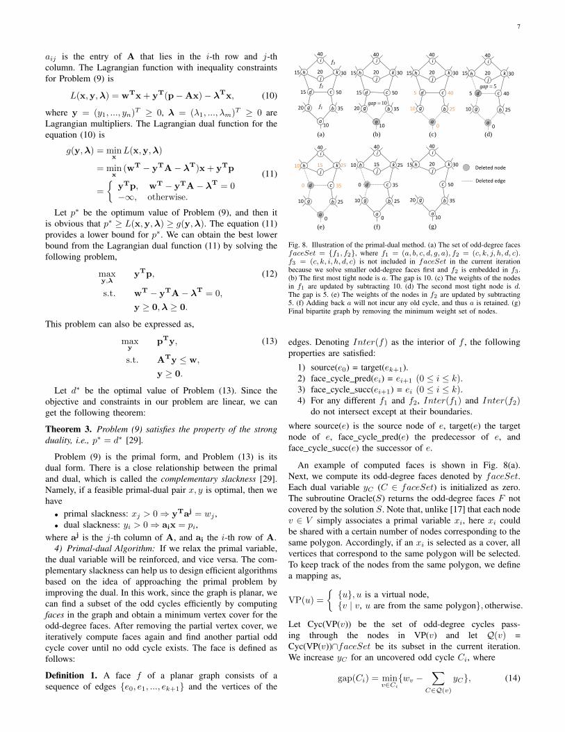
the dual variable will be reinforced, and vice versa. The com-plementary slackness can help us to design efficient algorithmsbased on the idea of approaching the primal problem byimproving the dual. In this work, since the graph is planar, wecan find a subset of the odd cycles efficiently by computingfaces in the graph and obtain a minimum vertex cover for theodd-degree faces. After removing the partial vertex cover, weiteratively compute faces again and find another partial oddcycle cover until no odd cycle exists. The face is defined asfollows:
Definition 1. A face f of a planar graph consists of asequence of edges {e0, e1, ..., ek+1} and the vertices of the
(b)
g b
cd
i
h
a
jk
10
35
40
15 30
20
15 50
20
(c)
(e)
g b
cd
i
h
a
jk
0
25
40
15 30
10
5 40
20
5gap
(f)
g b
cd
i
h
a
jk
0
25
40
10 25
10
0 35
15
(d)
g b
cd
i
h
a
jk
0
25
40
15 30
10
5 40
20
(g)
g b
c
i
h
a
jk
10
35
40
15 30
20
50
20
10gap
g b
cd
i
h
a
jk
0
25
40
10 25
10
0 35
15
f1g b
cd
i
h
f2
f3
a
jk
10
35
40
15 30
20
15 50
20
Deleted node
Deleted edge
(a)
Fig. 8. Illustration of the primal-dual method. (a) The set of odd-degree facesfaceSet = {f1, f2}, where f1 = (a, b, c, d, g, a), f2 = (c, k, j, h, d, c).f3 = (c, k, i, h, d, c) is not included in faceSet in the current iterationbecause we solve smaller odd-degree faces first and f2 is embedded in f3.(b) The first most tight node is a. The gap is 10. (c) The weights of the nodesin f1 are updated by subtracting 10. (d) The second most tight node is d.The gap is 5. (e) The weights of the nodes in f2 are updated by subtracting5. (f) Adding back a will not incur any old cycle, and thus a is retained. (g)Final bipartite graph by removing the minimum weight set of nodes.
edges. Denoting Inter(f) as the interior of f , the followingproperties are satisfied:
1) source(e0) = target(ek+1).2) face cycle pred(ei) = ei+1 (0 ≤ i ≤ k).3) face cycle succ(ei+1) = ei (0 ≤ i ≤ k).4) For any different f1 and f2, Inter(f1) and Inter(f2)
do not intersect except at their boundaries.
where source(e) is the source node of e, target(e) the targetnode of e, face cycle pred(e) the predecessor of e, andface cycle succ(e) the successor of e.
An example of computed faces is shown in Fig. 8(a).Next, we compute its odd-degree faces denoted by faceSet.Each dual variable yC (C ∈ faceSet) is initialized as zero.The subroutine Oracle(S) returns the odd-degree faces F notcovered by the solution S. Note that, unlike [17] that each nodev ∈ V simply associates a primal variable xi, here xi couldbe shared with a certain number of nodes corresponding to thesame polygon. Accordingly, if an xi is selected as a cover, allvertices that correspond to the same polygon will be selected.To keep track of the nodes from the same polygon, we definea mapping as,
VP(u) =
{{u}, u is a virtual node,{v | v, u are from the same polygon}, otherwise.
Let Cyc(VP(v)) be the set of odd-degree cycles pass-ing through the nodes in VP(v) and let Q(v) =Cyc(VP(v))∩faceSet be its subset in the current iteration.We increase yC for an uncovered odd cycle Ci, where
gap(Ci) = minv∈Ci
{wv −∑
C∈Q(v)
yC}, (14)

8
Algorithm 1 Planar Primal DualInput: G = (V,E): a planar graphOutput: S: a minimum weighted subset of V , covering all the odd
cycles1: S ← ∅2: gap(v)← wv, ∀v ∈ V3: while an odd cycle exists do4: Remove all non-cyclable edges of G5: faceSet← compute odd faces(G)6: while Oracle(S) 6= ∅ do7: F ← Oracle(S) /* Return odd faces not covered by S */8: for Ci ∈ F do9: vtight ← argminv∈Ci
{gap(v)}10: for v ∈ Ci do11: gap(v)← gap(v)− gap(vtight)12: end for13: S ← S ∪VP(vtight)14: end for15: end while16: Remove S and its associated edges from G17: end while18: /* Post-PD greedy refinement */19: Sort S in decreasing order according to the weight20: for v ∈ S do21: if S\VP(v) is a feasible odd cycle cover then22: S ← S\VP(v)23: end if24: end for
and the corresponding tight node,
vtight = arg minv∈Ctight
{wv −∑
C∈Q(v)
yC}. (15)
Note that in the actual implementation, we don’t need toexplicitly store the dual variables yC . Instead, a variable namedgap(v) is used for each vertex v to store the cumulativesubtraction from the dual variables, where the initialized valueis the weight of the vertex:
gap(v) ≡ wv −∑
C∈Q(v)
yC . (16)
Then gap(v) is updated by gap(v) − gap(vtight) for all v ∈Ci and VP(vtight) is added to S. An example is shown inFig. 8. Continue executing this until Oracle(S) is empty. Afterremoving S and the associated edges, we will compute thefaces again and re-conduct the above steps iteratively untilall odd cycles are covered. To further improve the quality ofsolution, after sorting S in decreasing order, if S\VP(v) isa feasible solution, then VP(vtight) will be removed from S.An example is shown in Fig. 8(e) and (f), where the node ais added back. The details of this algorithm are described inAlg. 1.
5) Resolving Remaining Conflicts: After solving the MVD-B problem on the maximum planar subgraph, we add backthe non-planar edges, which are removed in the first step.If a non-planar edge does not lead to a conflict, it will beretained. For those conflicting non-planar edges, we constructa remaining conflict graph Grem and find a minimum weightedvertex cover to eliminate the conflicts.
Algorithm 2 Non Planar Primal DualInput: G = (V,E): a general graphOutput: S: a minimum weighted subset of V , whose removal will
make the remaining graph bipartite1: S ← ∅2: gap(v)← wv, ∀v ∈ V3: while G is not bipartite do4: Find an odd cycle C from G using a DFS5: vtight ← argminv∈C{gap(v)}6: for v ∈ C do7: gap(v)← gap(v)− gap(vtight)8: end for9: S ← S ∪VP(vtight)
10: Remove VP(vtight) and its associated edges from G11: end while12: /* Post-PD greedy refinement */13: Sort S in decreasing order according to the weight of nodes14: for v ∈ S do15: if S\VP(v) is a feasible solution then16: S ← S\VP(v)17: end if18: end for
B. Primal-Dual Method for Non-Planar Graphs
In Sec. V-A, we have introduced a version of primal-dualmethod, which has also been presented in our preliminaryconference paper [1]. It is inspired by the following twoaspects: (1) Previous works (e.g. [21], [28]) mentioned the(nearly) planarity of the underlying conflict graphs. (2) It hasbeen proved that the primal-dual algorithm in [17] can obtain9/4 performance guarantee for planar graphs.
However, the planarization process is quite tricky so thatthe overall primal-dual method might not be effective. In thissection, we introduce a more general primal-dual method asshown in Alg. 2, which is almost the same as the previousmethod except that it does not require any planarizationprocess. An odd cycle is directly obtained by a depth-firstsearch, which requires a linear run time. However, we foundthat this non-planar primal-dual method can usually give abetter overall runtime performance for the benchmarks in ourexperiments. The algorithm works as follows: (1) It traversesthe graph G to find an odd cycle C (Line 4); (2) Next, it findsthe most tight node vtight in C (Line 5); (3) The gaps of eachnode are updated (Lines 6 to 8); (4) Add VP(vtight) to thesolution and remove it from G (Lines 9 and 10); (5) Continueuntil G is bipartite. Finally, similar to the planar primal-dualmethod, a post greedy refinement is conducted to add backthe nodes that will not incur any odd cycles.
C. Co-optimization of MPL Decomposition and EBL Usage
In this section, we introduce a random-initialized iterativeimprovement local search method for the co-optimization ofMPL decomposition and EBL throughput. The underlying ideaof the local search is rather simple. However, practically it canachieve good results.
Let P = {P1, ..., PK , PK+1} be the solution of the co-optimization of MPL and EBL, where Pi (i = 1, ...,K) isthe set of nodes assigned to the i-th mask of MPL, PK+1 isthe node set for EBL. Let m(P ) : P 7→ R be the measure of
9
Algorithm 3 Randomized Iterative ImprovementInput: G = (V,E): a conflict graph
K: the number of masks for MPLOutput: Pbest: the solution of co-optimization of MPL and EBL
1: for l = 0, ..., NRmax do2: Let {P (l)
1 , ..., P(l)K , P
(l)K+1} be a random initialization
3: P ← {P (l)1 , ..., P
(l)K , P
(l)K+1}
4: Count← 1, i← 15: while Improve(P ) and Count < MaxIter do6: Compute D(Pi)7: if m(D(Pi)) < m(P ) then8: P ← D(Pi)9: end if
10: Count← Count+ 111: i← 1 + (Count mod K)12: end while13: if l = 0 or m(Pbest) < m(P ) then14: Pbest ← P15: end if16: end for
the solution P . We obtain a neighbor of P by computing theperturbation D(Pi) of Pi, which is defined as follows:
D(Pi) = {P1, ..., P′i , P
′j , ..., PK , P
′K+1}, (17)
j = 1 + (i mod K), (18)
(P ′i , P′j , P
′K+1) = MVDB Solver(Gs), (19)
Gs = (Pi ∪ Pj ∪ PK+1, E(Pi ∪ Pj ∪ PK+1)), (20)
where i ∈ (1, ...,K), MVDB Solver(Gs) is the MVDB solver,E(Pi ∪ Pj ∪ PK+1) is the set of edges whose vertices are inPi ∪ Pj ∪ PK+1.
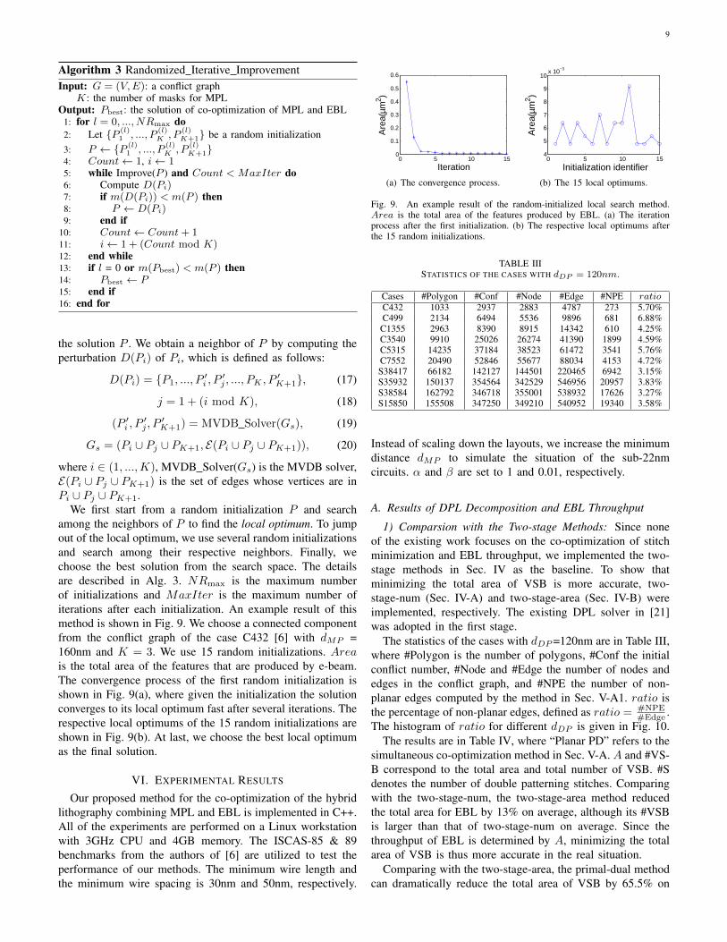
We first start from a random initialization P and searchamong the neighbors of P to find the local optimum. To jumpout of the local optimum, we use several random initializationsand search among their respective neighbors. Finally, wechoose the best solution from the search space. The detailsare described in Alg. 3. NRmax is the maximum numberof initializations and MaxIter is the maximum number ofiterations after each initialization. An example result of thismethod is shown in Fig. 9. We choose a connected componentfrom the conflict graph of the case C432 [6] with dMP =160nm and K = 3. We use 15 random initializations. Areais the total area of the features that are produced by e-beam.The convergence process of the first random initialization isshown in Fig. 9(a), where given the initialization the solutionconverges to its local optimum fast after several iterations. Therespective local optimums of the 15 random initializations areshown in Fig. 9(b). At last, we choose the best local optimumas the final solution.
VI. EXPERIMENTAL RESULTS
Our proposed method for the co-optimization of the hybridlithography combining MPL and EBL is implemented in C++.All of the experiments are performed on a Linux workstationwith 3GHz CPU and 4GB memory. The ISCAS-85 & 89benchmarks from the authors of [6] are utilized to test theperformance of our methods. The minimum wire length andthe minimum wire spacing is 30nm and 50nm, respectively.
0 5 10 150
0.1
0.2
0.3
0.4
0.5
0.6
Iteration
Are
a(µm
2 )
(a) The convergence process.
0 5 10 154
5
6
7
8
9
10x 10−3
Initialization identifier
Are
a(µm
2 )
(b) The 15 local optimums.
Fig. 9. An example result of the random-initialized local search method.Area is the total area of the features produced by EBL. (a) The iterationprocess after the first initialization. (b) The respective local optimums afterthe 15 random initializations.
TABLE IIISTATISTICS OF THE CASES WITH dDP = 120nm.
Cases #Polygon #Conf #Node #Edge #NPE ratioC432 1033 2937 2883 4787 273 5.70%C499 2134 6494 5536 9896 681 6.88%
C1355 2963 8390 8915 14342 610 4.25%C3540 9910 25026 26274 41390 1899 4.59%C5315 14235 37184 38523 61472 3541 5.76%C7552 20490 52846 55677 88034 4153 4.72%S38417 66182 142127 144501 220465 6942 3.15%S35932 150137 354564 342529 546956 20957 3.83%S38584 162792 346718 355001 538932 17626 3.27%S15850 155508 347250 349210 540952 19340 3.58%
Instead of scaling down the layouts, we increase the minimumdistance dMP to simulate the situation of the sub-22nmcircuits. α and β are set to 1 and 0.01, respectively.
A. Results of DPL Decomposition and EBL Throughput
1) Comparsion with the Two-stage Methods: Since noneof the existing work focuses on the co-optimization of stitchminimization and EBL throughput, we implemented the two-stage methods in Sec. IV as the baseline. To show thatminimizing the total area of VSB is more accurate, two-stage-num (Sec. IV-A) and two-stage-area (Sec. IV-B) wereimplemented, respectively. The existing DPL solver in [21]was adopted in the first stage.
The statistics of the cases with dDP =120nm are in Table III,where #Polygon is the number of polygons, #Conf the initialconflict number, #Node and #Edge the number of nodes andedges in the conflict graph, and #NPE the number of non-planar edges computed by the method in Sec. V-A1. ratio isthe percentage of non-planar edges, defined as ratio = #NPE
#Edge .The histogram of ratio for different dDP is given in Fig. 10.
The results are in Table IV, where “Planar PD” refers to thesimultaneous co-optimization method in Sec. V-A. A and #VS-B correspond to the total area and total number of VSB. #Sdenotes the number of double patterning stitches. Comparingwith the two-stage-num, the two-stage-area method reducedthe total area for EBL by 13% on average, although its #VSBis larger than that of two-stage-num on average. Since thethroughput of EBL is determined by A, minimizing the totalarea of VSB is thus more accurate in the real situation.
Comparing with the two-stage-area, the primal-dual methodcan dramatically reduce the total area of VSB by 65.5% on

10
TABLE IVCO-OPTIMIZATION RESULTS OF DPL STITCH MINIMIZATION AND EBL UTILIZATION WITH dDP = 120nm.
Cases Two-stage-num Two-stage-area Planar PDA(µm2) #VSB #S Time(s) A(µm2) #VSB #S Time(s) A(µm2) #VSB #S Time(s)
C432 1.87 328 9 0.14 1.35 339 17 0.13 0.58 251 4 0.14C499 4.62 867 18 0.57 4.24 875 15 0.57 1.91 753 5 0.51
C1355 6.16 787 59 0.28 5.25 783 63 0.28 1.69 630 17 0.34C3540 29.73 2781 174 1.14 26.60 2856 178 1.14 7.99 2677 79 1.32C5315 37.25 3655 366 1.62 32.10 3667 421 1.61 11.38 3571 126 1.88C7552 53.74 5680 340 2.07 45.41 5603 361 2.07 14.91 4948 140 2.41S38417 183.31 18624 1184 4.39 156.38 18844 1195 4.40 53.14 16743 384 4.55S35932 425.22 46742 3074 13.39 379.21 47252 3172 13.43 133.32 39583 954 13.54S38584 427.00 45525 3554 11.57 364.36 46266 3543 11.58 132.60 40654 1005 11.61S15850 465.13 46723 3252 11.75 410.40 46785 3290 11.72 134.65 41864 1060 11.98
Avg. 3.32 1.13 3.19 0.97 2.90 1.14 3.25 1.00 1.00 1.00 1.00 1.00
TABLE VCOMPARISON BETWEEN ILP METHOD AND PRIMAL DUAL METHOD WITH dDP = 100nm.
Cases ILP Planar PD Non-planar PDA(µm2) #VSB #S Time(s) A(µm2) #VSB #S Time(s) A(µm2) #VSB #S Time(s)
C432 0.51 227 8 1.56 0.51 229 8 0.09 0.54 237 9 0.01C499 1.55 684 49 34957.80 1.60 688 43 0.37 1.56 682 40 0.01C1355 1.15 486 68 4.83 1.19 506 67 0.19 1.21 503 64 0.02C3540 5.22 2184 502 266.44 5.57 2235 468 0.97 5.63 2255 434 0.06C5315 7.31 3072 775 111.71 7.81 3132 727 1.20 7.75 3106 657 0.09C7552 10.21 4175 888 5778.89 10.84 4267 854 1.59 10.75 4234 812 0.13S38417 NA NA NA >7714Min 36.56 13265 2089 3.68 35.87 13203 2034 0.39S35932 NA NA NA >7714Min 101.22 33033 4899 11.28 98.20 32499 5031 1.03S38584 NA NA NA >7714Min 95.93 33181 5377 9.64 94.80 32965 5451 1.03S15850 NA NA NA >7714Min 98.94 35179 6040 9.70 97.44 35062 5948 1.05
Avg. NA NA NA NA 1.02 1.01 1.00 10.13 1.00 1.00 1.00 1.00Note: NA - Not available, Min - Minutes.
TABLE VIPLANAR PD WITH DIFFERENT MAXIMUM PLANAR SUBGRAPH FINDING ALGORITHMS (dDP = 100nm).
Cases CT + Planar PD GCT + Planar PDA(µm2) #VSB #S Time(s) A(µm2) #VSB #S Time(s)
C432 0.65 246 12 0.03 0.51 229 8 0.09C499 2.58 822 88 0.06 1.60 688 43 0.37
C1355 1.35 547 83 0.08 1.19 506 67 0.19C3540 7.23 2505 528 0.25 5.57 2235 468 0.97C5315 11.26 3636 861 0.38 7.81 3132 727 1.20C7552 14.25 4714 1013 0.54 10.84 4267 854 1.59S38417 58.77 15703 2631 1.53 36.56 13265 2089 3.68S35932 164.19 40175 6826 3.83 101.22 33033 4899 11.28S38584 141.99 38518 6874 3.72 95.93 33181 5377 9.64S15850 160.75 41919 7679 3.80 98.94 35179 6040 9.70
Avg. 1.56 1.18 1.29 0.37 1.00 1.00 1.00 1.00
average with more or less the same runtime. Besides, theprimal-dual method can also significantly reduce the numberof stitches by 69.2% on average. Note that less total area forVSB means a higher throughput for EBL and that less stitchesmean lower manufacturing cost for DPL. Thus, our primal-dual method can simultaneously improve the throughput andreduce the manufacturing cost comparing with the two-stagemethods. Therefore, the experimental results further demon-strate the effectiveness of our proposed primal-dual method.
Note that DPL+EBL is different from TPL. In TPL, thereare unresolvable conflicts as shown in Fig. 11(c), which canmake the whole chip failed. In DPL+EBL, there are nounresolvable conflicts (assuming the writing resolution of EBLis sufficient) because all the unresolvable conflicts can beresolved by e-beam direct writing.
Fig. 12 shows the DPL+EBL decomposition result for C432.
Fig. 10. Histogram of the percent of non-planar edges for different dDP .
2) Comparison with the ILP-based Method: In this experi-ment, we compare our primal-dual method with the ILP-based
11
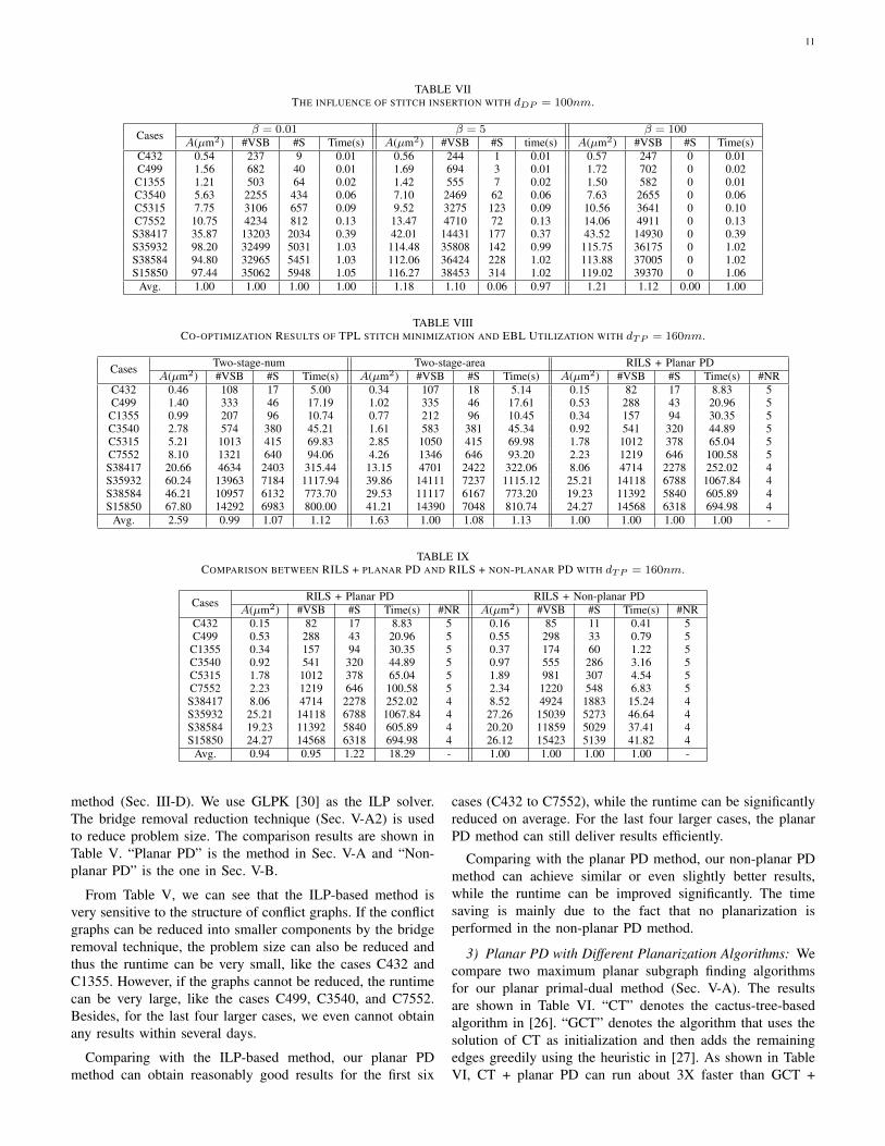
TABLE VIITHE INFLUENCE OF STITCH INSERTION WITH dDP = 100nm.
Cases β = 0.01 β = 5 β = 100A(µm2) #VSB #S Time(s) A(µm2) #VSB #S time(s) A(µm2) #VSB #S Time(s)
C432 0.54 237 9 0.01 0.56 244 1 0.01 0.57 247 0 0.01C499 1.56 682 40 0.01 1.69 694 3 0.01 1.72 702 0 0.02
C1355 1.21 503 64 0.02 1.42 555 7 0.02 1.50 582 0 0.01C3540 5.63 2255 434 0.06 7.10 2469 62 0.06 7.63 2655 0 0.06C5315 7.75 3106 657 0.09 9.52 3275 123 0.09 10.56 3641 0 0.10C7552 10.75 4234 812 0.13 13.47 4710 72 0.13 14.06 4911 0 0.13S38417 35.87 13203 2034 0.39 42.01 14431 177 0.37 43.52 14930 0 0.39S35932 98.20 32499 5031 1.03 114.48 35808 142 0.99 115.75 36175 0 1.02S38584 94.80 32965 5451 1.03 112.06 36424 228 1.02 113.88 37005 0 1.02S15850 97.44 35062 5948 1.05 116.27 38453 314 1.02 119.02 39370 0 1.06
Avg. 1.00 1.00 1.00 1.00 1.18 1.10 0.06 0.97 1.21 1.12 0.00 1.00
TABLE VIIICO-OPTIMIZATION RESULTS OF TPL STITCH MINIMIZATION AND EBL UTILIZATION WITH dTP = 160nm.
Cases Two-stage-num Two-stage-area RILS + Planar PDA(µm2) #VSB #S Time(s) A(µm2) #VSB #S Time(s) A(µm2) #VSB #S Time(s) #NR
C432 0.46 108 17 5.00 0.34 107 18 5.14 0.15 82 17 8.83 5C499 1.40 333 46 17.19 1.02 335 46 17.61 0.53 288 43 20.96 5C1355 0.99 207 96 10.74 0.77 212 96 10.45 0.34 157 94 30.35 5C3540 2.78 574 380 45.21 1.61 583 381 45.34 0.92 541 320 44.89 5C5315 5.21 1013 415 69.83 2.85 1050 415 69.98 1.78 1012 378 65.04 5C7552 8.10 1321 640 94.06 4.26 1346 646 93.20 2.23 1219 646 100.58 5S38417 20.66 4634 2403 315.44 13.15 4701 2422 322.06 8.06 4714 2278 252.02 4S35932 60.24 13963 7184 1117.94 39.86 14111 7237 1115.12 25.21 14118 6788 1067.84 4S38584 46.21 10957 6132 773.70 29.53 11117 6167 773.20 19.23 11392 5840 605.89 4S15850 67.80 14292 6983 800.00 41.21 14390 7048 810.74 24.27 14568 6318 694.98 4
Avg. 2.59 0.99 1.07 1.12 1.63 1.00 1.08 1.13 1.00 1.00 1.00 1.00 -
TABLE IXCOMPARISON BETWEEN RILS + PLANAR PD AND RILS + NON-PLANAR PD WITH dTP = 160nm.
Cases RILS + Planar PD RILS + Non-planar PDA(µm2) #VSB #S Time(s) #NR A(µm2) #VSB #S Time(s) #NR
C432 0.15 82 17 8.83 5 0.16 85 11 0.41 5C499 0.53 288 43 20.96 5 0.55 298 33 0.79 5
C1355 0.34 157 94 30.35 5 0.37 174 60 1.22 5C3540 0.92 541 320 44.89 5 0.97 555 286 3.16 5C5315 1.78 1012 378 65.04 5 1.89 981 307 4.54 5C7552 2.23 1219 646 100.58 5 2.34 1220 548 6.83 5S38417 8.06 4714 2278 252.02 4 8.52 4924 1883 15.24 4S35932 25.21 14118 6788 1067.84 4 27.26 15039 5273 46.64 4S38584 19.23 11392 5840 605.89 4 20.20 11859 5029 37.41 4S15850 24.27 14568 6318 694.98 4 26.12 15423 5139 41.82 4
Avg. 0.94 0.95 1.22 18.29 - 1.00 1.00 1.00 1.00 -
method (Sec. III-D). We use GLPK [30] as the ILP solver.The bridge removal reduction technique (Sec. V-A2) is usedto reduce problem size. The comparison results are shown inTable V. “Planar PD” is the method in Sec. V-A and “Non-planar PD” is the one in Sec. V-B.
From Table V, we can see that the ILP-based method isvery sensitive to the structure of conflict graphs. If the conflictgraphs can be reduced into smaller components by the bridgeremoval technique, the problem size can also be reduced andthus the runtime can be very small, like the cases C432 andC1355. However, if the graphs cannot be reduced, the runtimecan be very large, like the cases C499, C3540, and C7552.Besides, for the last four larger cases, we even cannot obtainany results within several days.
Comparing with the ILP-based method, our planar PDmethod can obtain reasonably good results for the first six
cases (C432 to C7552), while the runtime can be significantlyreduced on average. For the last four larger cases, the planarPD method can still deliver results efficiently.
Comparing with the planar PD method, our non-planar PDmethod can achieve similar or even slightly better results,while the runtime can be improved significantly. The timesaving is mainly due to the fact that no planarization isperformed in the non-planar PD method.
3) Planar PD with Different Planarization Algorithms: Wecompare two maximum planar subgraph finding algorithmsfor our planar primal-dual method (Sec. V-A). The resultsare shown in Table VI. “CT” denotes the cactus-tree-basedalgorithm in [26]. “GCT” denotes the algorithm that uses thesolution of CT as initialization and then adds the remainingedges greedily using the heuristic in [27]. As shown in TableVI, CT + planar PD can run about 3X faster than GCT +

12
(a) DPL. (b) DPL+EBL.
(c) TPL. (d) TPL+EBL.
Fig. 11. Comparison between DPL, DPL+EBL, TPL, and TPL+EBL for a45nm cell. The blue color is for EBL, while the others are for different masksof MPL. The blue line indicates unresolved conflicts. dMP =200nm.
Fig. 12. The DPL+EBL decomposition result for C432. The blue color is forEBL. The other two colors are for different masks of DPL.
planar PD on average, while the solution quality of GCT +planar PD can be much better than that of CT + planar PD.A better planarization algorithm usually can directly benefitour planar PD method. Therefore, we expect that if there is aplanarization algorithm as fast as CT while its solution qualitycan match or outperform GCT, our planar PD method mayachieve better runtime performance.
4) Influence of Stitch Insertion: In this experiment, westudy the influence of stitch insertion in the DPL+EBL de-composition. The e-beam area weight α is fixed to 1. Thestitch weight β is set to 0.01, 5, and 100, respectively. Theresults are shown in Table VII. We use the non-planar PDmethod (Sec. V-B) as the MVDB solver. dDP =100nm.
We can see that if β is set to 0.01 (i.e., the stitch weightis very small compared with the e-beam area weight), stitcheswill be sacrificed to save e-beam usage. However, when β isset to 100 (i.e., the stitch weight is very large compared withthe e-beam area weight), no stitches will be used and the totalarea of e-beam will be increased by 21% on average to solvethe conflicts in the layout. When β is set to a value between0.01 and 100, the primal-dual method will make a tradeoff to
solve the conflicts according to the weights of each other. Notethat different foundries or hybrid lithography systems mighthave different requirement on the stitch weight. In practice,the weights should be set by the designers or manufacturersto control the manufacturing cost and improve the throughputsimultaneously.
B. Results of TPL Decomposition and EBL Throughput
1) Comparison with the Two-stage Methods: With thedecreased feature size, DPL is not sufficient. Thus TPL isproposed as shown in Fig. 11(c). We implemented the versionof the two-stage methods for the hybrid lithography of TPLand EBL. The existing TPL decomposer in [9] is used in thefirst stage. The detailed results are reported in Table VIII.“RILS” denotes the random-initialized local search method inSec. V-C, and #NR denotes the number of initializations. Com-paring with the two-stage-num, the two-stage-area methodreduced the total area for EBL by more than 37% on average,although its #VSB is larger than that of two-stage-area exceptthe case C432. Thus, this result further verifies that minimizingA is more accurate. Comparing with the two-stage-area, ourproposed RILS with the planar PD method can further reducethe total area for EBL by 38.7% on average and can reduce thenumber of stitches by 7.4% on average simultaneously. Theruntime of our proposed RILS method is more or less the sameas the two stage method. Therefore, the experimental resultsdemonstrate the effectiveness of the proposed RILS method.
Note that our proposed framework can handle with con-strained decomposition for the hybrid lithography of MPL andEBL by pre-processing the conflict graph and color permu-tations. The constrained decomposition requires that certainfeatures in the layout should be assigned to a certain mask,which is very useful in a practical flow. The co-optimizationresult of a 45nm layout with PG straps by our RILS with theplanar PD method is shown in Fig. 13, where the P&G net isconstrained to be assigned to Mask 1.
2) RILS with Different MVDB Solvers: In this experiment,we compare the RILS + planar PD method with the RILS +non-planar PD method. The results are shown in Table IX.#NR is the number of random initializations. From the table,we can see that the RILS + non-planar PD method can achievemore or less the same results comparing with the RILS +planar PD method. The total e-beam area is increased by 6%on average, while the number of stitches is decreased by 18%on average. However, the runtime of the RILS + non-planarPD method is improved significantly.
VII. CONCLUSION
The hybrid lithography combining LELE-style MPL and E-BL is promising with the decreased feature size. We introducea new layout decomposition framework for the MPL+EBL hy-brid lithography, which considers the stitch minimization andEBL throughput simultaneously. To do that, we have proposedthe planar primal-dual method for the co-optimization of DPLand EBL, and the random-initialized local search method forthat of MPL and EBL. Experimental results demonstrate theefficiency of our proposed methods.

13
Mask 1 Mask 2 Mask 3 VSB
Fig. 13. The co-optimization of TPL and EBL for a 45nm layout. The P&Gnet is constrained to be assigned to Mask 1.
We have also introduced a non-planar primal-dual methodwhich can achieve more or less the same quality of resultswhile the runtime can be improved significantly. We have alsodiscussed how to reduce the stage movement and settling timeto further improve the throughput on a typical EBL system.
ACKNOWLEDGEMENT
The authors would like to thank Prof. Yifang Chen fromState Key Lab. of ASIC and System in Fudan University forproviding the EBL system data and calculating the e-beamexposure time. We would like to thank Prof. Walter Hu fromUT Dallas for helpfull discussion about EBL system. Wewould also like to thank the anonymous reviewers for theirconstructive comments.
REFERENCES
[1] Y. Yang, W.-S. Luk, H. Zhou, C. Yan, X. Zeng, and D. Zhou, “Layout de-composition co-optimization for hybrid e-beam and multiple patterninglithography,” in IEEE/ACM Asia and South Pacific Design AutomationConference (ASPDAC), 2015.
[2] K. Yuan, B. Yu, and D. Z. Pan, “E-beam lithography stencil planningand optimization with overlapped characters,” IEEE Transactions onComputer-Aided Design of Integrated Circuits and Systems, vol. 31,no. 2, pp. 167–179, 2012.
[3] A. Kahng, C.-H. Park, X. Xu, and H. Yao, “Layout decompositionapproaches for double patterning lithography,” IEEE Transactions onComputer-Aided Design of Integrated Circuits and Systems, vol. 29,no. 6, pp. 939–952, 2010.
[4] K. Yuan, J.-S. Yang, and D. Z. Pan, “Double patterning layout de-composition for simultaneous conflict and stitch minimization,” IEEETransactions on Computer-Aided Design of Integrated Circuits andSystems, vol. 29, no. 2, pp. 185–196, 2010.
[5] X. Tang and M. Cho, “Optimal layout decomposition for double pattern-ing technology,” in IEEE/ACM International Conference on Computer-Aided Design (ICCAD), 2011, pp. 9–13.
[6] B. Yu, K. Yuan, D. Ding, and D. Pan, “Layout decomposition for triplepatterning lithography,” IEEE Transactions on Computer-Aided Designof Integrated Circuits and Systems, vol. 34, no. 3, pp. 433–446, 2015.
[7] S.-Y. Fang, Y.-W. Chang, and W.-Y. Chen, “A novel layout decompo-sition algorithm for triple patterning lithography,” IEEE Transactionson Computer-Aided Design of Integrated Circuits and Systems, vol. 33,no. 3, pp. 397–408, 2014.
[8] J. Kuang and E. F. Young, “An efficient layout decomposition approachfor triple patterning lithography,” in ACM/IEEE Design AutomationConference (DAC), 2013.
[9] Y. Zhang, W.-S. Luk, H. Zhou, C. Yan, and X. Zeng, “Layout de-composition with pairwise coloring for multiple patterning lithography,”in IEEE/ACM International Conference on Computer-Aided Design(ICCAD), 2013.
[10] S.-Y. Fang, S.-Y. Chen, and Y.-W. Chang, “Native-conflict and stitch-aware wire perturbation for double patterning technology,” IEEE Trans-actions on Computer-Aided Design of Integrated Circuits and Systems,vol. 31, no. 5, pp. 703–716, 2012.
[11] J. Sun, Y. Lu, H. Zhou, and X. Zeng, “Post-routing layer assignmentfor double patterning,” in IEEE/ACM Asia and South Pacific DesignAutomation Conference (ASPDAC), 2011, pp. 793–798.
[12] S. Steen, S. McNab, L. Sekaric, I. Babich, J. Patel, J. Bucchignano,M. Rooks, D. Fried, A. Topol, J. Brancaccio et al., “Looking into thecrystal ball: future device learning using hybrid e-beam and opticallithography (keynote paper),” in Microlithography 2005. InternationalSociety for Optics and Photonics, 2005, pp. 26–34.
[13] Y. Du, H. Zhang, M. D. Wong, and K.-Y. Chao, “Hybrid lithographyoptimization with e-beam and immersion processes for 16nm 1D griddeddesign,” in IEEE/ACM Asia and South Pacific Design AutomationConference (ASPDAC), 2012, pp. 707–712.
[14] Y. Ding, C. Chu, and W.-K. Mak, “Throughput optimization for SADPand e-beam based manufacturing of 1D layout,” in ACM/IEEE DesignAutomation Conference (DAC), 2014, pp. 1–6.
[15] J.-R. Gao, B. Yu, and D. Z. Pan, “Self-aligned double patterning layoutdecomposition with complementary e-beam lithography,” in IEEE/ACMAsia and South Pacific Design Automation Conference (ASPDAC), 2014,pp. 143–148.
[16] H. Tian, H. Zhang, Z. Xiao, and M. D. Wong, “Hybrid lithographyfor triple patterning decomposition and e-beam lithography,” in SPIEAdvanced Lithography. International Society for Optics and Photonics,2014, pp. 90 520P–90 520P.
[17] M. X. Goemans and D. P. Williamson, “Primal-dual approximationalgorithms for feedback problems in planar graphs,” Combinatorica,vol. 18, no. 1, pp. 37–59, 1998.
[18] J. M. Schmidt, “A simple test on 2-vertex- and 2-edge-connectivity,”Information Processing Letters, vol. 113, no. 7, pp. 241–244, 2013.
[19] S. Rizvi, Handbook of photomask manufacturing technology. CRCPress, 2005.
[20] N. W. Parker, A. D. Brodie, and J. H. McCoy, “High-throughput NGLelectron-beam direct-write lithography system,” in Microlithography2000. International Society for Optics and Photonics, 2000, pp. 713–720.
[21] W.-S. Luk and H. Huang, “Fast and lossless graph division methodfor layout decomposition using SPQR-tree,” in IEEE/ACM InternationalConference on Computer-Aided Design (ICCAD), 2010, pp. 112–115.
[22] G. Ausiello and et al, Complexity and Approximability Properties: Com-binatorial Optimization Problems and Their Approximability Properties.Springer, 1999.
[23] F. Hadlock, “Finding a maximum cut of a planar graph in polynomialtime,” SIAM Journal on Computing, vol. 4, no. 3, pp. 221–225, 1975.
[24] H.-A. Choi, K. Nakajima, and C. S. Rim, “Graph bipartization and viaminimization,” SIAM Journal on Discrete Mathematics, vol. 2, no. 1,pp. 38–47, 1989.
[25] B. Yu and D. Z. Pan, “Layout decomposition for quadruple patterninglithography and beyond,” in ACM/IEEE Design Automation Conference(DAC), 2014, pp. 1–6.
[26] G. Calinescu, C. G. Fernandes, U. Finkler, and H. Karloff, “A betterapproximation algorithm for finding planar subgraphs,” Journal ofAlgorithms, vol. 27, no. 2, pp. 269–302, 1998.
[27] T. Poranen, “Two new approximation algorithms for the maximumplanar subgraph problem.” Acta Cybern., vol. 18, no. 3, pp. 503–527,2008.
[28] Y. Xu and C. Chu, “A matching based decomposer for double patterninglithography,” in Proceedings of the 19th international symposium onPhysical design. ACM, 2010, pp. 121–126.
[29] C. H. Papadimitriou and K. Steiglitz, Combinatorial optimization:algorithms and complexity. Courier Dover Publications, 1982.
[30] A. Makhorin, “GLPK - the GNU linear programming toolkit,”http://www.gnu.org/directory/GNU/glpk.html, 2014.

14
Yunfeng Yang received the B.S. degree in informa-tion engineering from Southeast University, Nanjing,China, in 2008. He is currently pursuing the Ph.D.degree with State Kay Lab. of Application Specif-ic Integrated Circuits and System, MicroelectronicsDepartment, Fudan University, Shanghai, China.
He was with Synopsys, Shanghai, during thesummer of 2013, 2014, and 2015 as a software en-gineering R&D intern. His current research interestsinclude design for manufacturability, mathematicalmodeling, and optimization.
Wai-Shing Luk was graduated from Chinese Uni-versity of Hong Kong in 1988 with a B.Sc. degreein Electronics. He received his M.Phil. and Ph.D.degrees in Computer Science and Engineering fromthe same university in 1993 and 1996 respectively.In1997, he was awarded a postdoctoral fellowshipat Katholieke Universiteit Leuven in Belgium. Heworked as a Senior R&D Engineer at Synopsys inUS from 1999. After joining Fudan University as anAssociate Professor in 2004, he has published over30 papers in international conferences and reviewed
journals. His research interests include design for manufacturability, statisticalanalysis and optimization, and VLSI physical design algorithms.
David Z. Pan (S’97-M’00-SM’06-F’14) receivedthe B.S. degree from Peking University, Beijing,China, and the M.S. and Ph.D. degrees from theUniversity of California, Los Angeles, CA, USA.From 2000 to 2003, he was a Research Staff Memberat IBM T. J. Watson Research Center, YorktownHeights, NY, USA. He is currently the EngineeringFoundation Professor with the Department of Elec-trical and Computer Engineering, The Universityof Texas (UT) at Austin, Austin, TX, USA. Hiscurrent research interests include nanoscale design
for manufacturability and reliability, physical design, vertical integrationdesign and technology, and design/CAD for emerging technologies. He haspublished over 230 papers in refereed journals and conferences, and holdseight U.S. Patents.
He has served as a Senior Associate Editor for ACM Transactions onDesign Automation of Electronic Systems (TODAES), an Associate Editorfor IEEE Transactions on Computer Aided Design of Integrated Circuitsand Systems (TCAD), IEEE Transactions on Very Large Scale IntegrationSystems (TVLSI), IEEE Transactions on Circuits and Systems PART I(TCAS-I), IEEE Transactions on Circuits and Systems PART II (TCAS-II),Science China Information Sciences (SCIS), Journal of Computer Science andTechnology (JCST), IEEE CAS Society Newsletter, etc. He has served in theExecutive/Program Committees of many major conferences, including DesignAutomation Conference (DAC), International Conference on Computer AidedDesign (ICCAD), Asia and South Pacific Design Automation Conference(ASPDAC), and International Symposium on Physical Design (ISPD).
He was the recipient of the SRC 2013 Technical Excellence Award, theDAC Top Ten Author in Fifth Decade Award, the DAC Prolific Author Award,the Asia and South Pacific Design Automation Conference Frequently CitedAuthor Award in 2015, 12 Best Paper Awards at premier venues such asASPDAC, Design, Automation & Test in Europe (DATE), ICCAD, IBMResearch, ISPD, and SRC TECHCON, various international CAD Contestawards, the Communications of the ACM Research Highlights in 2014, theACM/SIGDA Outstanding New Faculty Award in 2005, the NSF CAREERAward in 2007, the SRC Inventor Recognition Award thrice, the IBM FacultyAward four times, the UCLA Engineering Distinguished Young AlumnusAward in 2009, the UT Austin RAISE Faculty Excellence Award in 2014,the UCLA Computer Science Department Outstanding PhD Award in 2000,the ACM Recognition of Service Award in 2007 and 2008, among others.From 2008 to 2009, he was an IEEE CAS Society Distinguished Lecturer.
Hai Zhou (SM’04) received the B.S. and M.S.degrees in computer science and technology fromTsinghua University, Beijing, China, in 1992 and1994, respectively, and the Ph.D. degree in computersciences from the University of Texas, Austin, in1999. He is currently an Associate Professor of Elec-trical Engineering and Computer Science with theDepartment of Electrical Engineering and ComputerScience, Northwestern University, Evanston, IL. Hiscurrent research interests include very large scaleintegration computer-aided design, algorithm design,
and formal methods. Dr. Zhou was a recipient of the CAREER Award fromthe National Science Foundation in 2003.
Changhao Yan received the B.E. and M.E. degreesin fluid mechanics and computer science from theHuazhong University of Science and Technology,Wuhan, China, in 1996 and 2002, respectively, andthe Ph.D. degree in computer science from TsinghuaUniversity, Beijing, China, in 2006. Currently, he is aLecturer with State Key Lab. of Application SpecificIntegrated Circuits and Systems, MicroelectronicsDepartment, Fudan University, Shanghai, China. Hiscurrent research interests include parasitic parameterextraction of interconnects, design for manufactura-
bility, chemical mechanical polishing modeling, and simulation.
Dian Zhou (M’89-SM’07) received the B.S degreein physics and M.S degree in electrical engineeringfrom Fudan University, China, in 1982 and 1985,respectively, and the Ph.D. degree in electrical andcomputer engineering from the University of Illinoisin 1990.
He joined the University of North Carolina atCharlotte as an assistant professor in 1990, wherehe became an associate professor in 1995. He joinedthe University of Texas at Dallas as a full professorin 1999. His research interests include: High-speed
VLSI systems, CAD tools, mixed-signal ICs, and algorithms.Dr. Zhou received the Research Initiation Award from National Science
Foundation in 1991, the IEEE Circuits and Systems and Society DarlingtonAward in 1993, and the National Science Foundation Young InvestigatorAward in 1994. He also served as a panel member of the NSF CAREERAward in 1996. He was a Guest Editor for the International Journal ofCustom-Chip Design, Simulation and Testing, and was an Associate Editorfor IEEE TRANSACTIONS ON CIRCUITS AND SYSTEMS from 1996 to1998. He received Chinese NSF Oversea’s Outstanding Young Scientist Awardin 2000, and Chinese Yangzi River Scholar from 2002 to 2007. He was thepanel member of ”Moving up the Technology Chain” at World EconomyForum, Davos, Switzerland, 2006. He received Changjiang Honor Professorfrom Fudan Uinversity in 2008, and was selected as ”Thousand People Plan”professor from China in 2011.
Xuan Zeng (M’97) received the B.Sc. and Ph.D.degrees in electrical engineering from Fudan Uni-versity, Shanghai, China, in 1991 and 1997.
She is currently a Full Professor with the Micro-electronics Department and serves as the Directorof State Key Laboratory of ASIC and System-s, Fudan University, Shanghai, China. She was aVisiting Professor with the Electrical EngineeringDepartment, Texas A&M University, College Sta-tion, and Microelectronics Department, TechnischeUniversiteit Delft, Delft, The Netherlands, in 2002
and 2003. Her research interests include design for manufacturability, high-speed interconnect analysis and optimization, analog behavioral modeling,circuit simulation, and ASIC design.
Dr. Zeng was a recipient of the first-class Award of Electronic InformationScience and Technology from the Chinese Institute of Electronics in 2005. Shereceived the second-class Award of Science and Technology Advancementand the Cross-Century Outstanding Scholar Award from the Ministry ofEducation of China in 2006 and 2002. She received the award of IT Top10 in Shanghai in 2003. She served on the Technical Program Committeeof the IEEE/Association for Computing Machinery Asia and South PacificDesign Automation Conference in 2000 and 2005.