Embed Size (px)
Citation preview
LayeredProtocolWrappers forInter net Packet Processingin ReconfigurableHardware
FlorianBraun,JohnLockwood,MarcelWaldvogel
WUCS-01-10
July, 2001
Departmentof ComputerScienceAppliedResearchLabWashingtonUniversityCampusBox 1045OneBrookingsDriveSaintLouis,MO 63130
Abstract
A library of layeredprotocolwrappershasbeendevelopedthatprocessInterentpacketsin reconfigurablehardware.Thesewrapperscanbeusedwith a reprogrammablenetwork platformcalledtheField ProgrammablePortExtender(FPX) to rapidly prototypehardwarecircuits for processingInternetpackets. We presenta framework to streamlineandsimplify thedevelopmentof networkingapplicationsthatprocessATM cells,AAL5 frames,InternetProtocol(IP)packetsandUDPdatagramsdirectly in hardware.
Supportedby: NSFANI-0096052andXilinx Corp.
1
1 Intr oduction
In recentyears,Field ProgrammableGateArrays (FPGAs)have becomesufficiently capableto implementcomplexnetworking applicationsdirectly in hardware. By usinghardwarethatcanbereprogrammednetwork equipmentcandynamicallyload new functionality. Sucha featureallows, for example,firewalls to addnew filters that canrun atline speed.TheField ProgrammablePortExtenderhasbeenimplementedasa flexible platformfor theprocessingofnetwork datain hardware. The library of wrappersdiscussedin this paperallows applicationsto be developedthatprocessdataatseverallayersof theprotocolstack.Layersareimportantfor networksbecausethey allow applicationsto be implementedat a level wherethe detailsof a protocollayer canbe abstractedfor layersabove. At the lowestlayer, networks modify raw datathat passesbetweeninterfaces.At higher levels, the applicationsprocessvariablelengthframesor packagesasin theInternetProtocol.At theuser-level, applicationsmaytransmitor receivemessagesin UserDatagramProtocolmessages.An Internetrouteror firewall areimportantapplicationsthatusethe wrapperlibrary to routeandfilter packets.
2 Background
In theApplied ResearchLab at WashingtonUniversity in St. Louis, a rich setof hardwareandsoftwarecomponentsfor researchin the field of networking, switching, routing andactive networking have beendeveloped. The FieldProgrammableportextenderhasbeendevelopedto enablemodularcomponentsto beimplementedin reprogrammablehardware. Themodulesdescribedin this documentareprimarily targetedto this kit, thoughthedesignis written inportableVHDL andcouldbeusedin any FPGA-basedsystem.
2.1 Switch Fabric
The centralcomponentof this researchenvironmentis the WashingtonUniversity Gigabit Switch (WUGS) [1]. Itis a fully featured8-port ATM switch,which is capableof handlingup to 20 Gbpsof network traffic. Eachport isconnectedthrougha line cardto the switch. The WUGS providesspaceto insertextensioncardsbetweenthe linecardsandthebackbone.
2.2 Field ProgrammablePort Extender
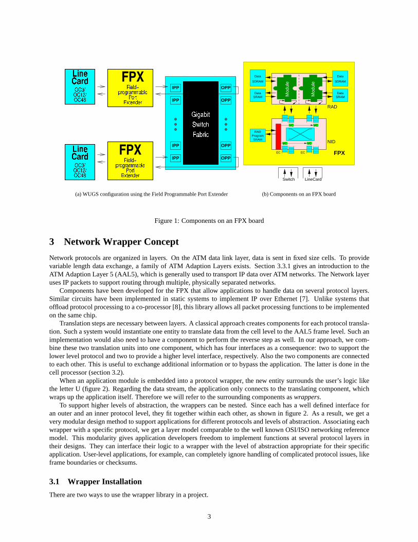
TheFieldProgrammablePortExtender(FPX) [2, 3] providesreprogrammablelogic for userapplications.It providesinterfacesto boththeswitchandtheline-card,soit canbeinsertedbetweenthesetwo cards,asillustratedin figure1(a).
TheFPXcontainstwo FPGAs:theNetwork InterfaceDevice (NID) andtheReprogrammableApplicationDevice(RAD). TheNID interconnectstheWUGS,theline cardandtheRAD via anon-chipATM switchcore.It alsoprovidesthelogic to dynamicallyreprogramtheRAD. TheRAD canbeprogrammedto holduser-definedmodules.Thisfeatureenablesuser-definednetwork modulesto bedynamicallyloadedinto thesystem.TheRAD is alsoconnectedto twoSRAM and two SDRAM components.The memorymodulescanbe usedto cachecell dataor hold large tables.Figure1(b) illustratesthemajorcomponentson anFPX board.
2.3 FPX Modules
Userapplicationsareimplementedon theRAD asmodules.Modulesarehardwarecomponentswith a well-definedinterfacewhich communicatewith theRAD andotherinfrastructurecomponents.Thebasicdatainterfaceis a 32-bitwideUtopiainterface.InternetpacketsenterthemoduleusingclassicalIP overATM encapsulationandsegmentationinto ATM cells. Thedatabuscarriesheaderandpayloadof the cells. Theothersignalsin the moduleinterfaceareusedfor congestioncontrolandto connectto memorycontrollersto accesstheoff-chip memory. Thecompletemoduleinterfaceis documentedin [4, 5].
Usually, two applicationmodulesarepresenton the RAD. Typically, onehandlesdatafrom the line cardto theswitch(ingress)andtheotherhandlesdatafrom theswitchto theline card(egress).As with theTransmutableTelecomSystem[6], modulescanbereplacedby reprogrammingtheFPGAin thesystemat any time. In thecaseof theFPX,this functionality occursvia partial reprogrammingof the RAD FPGA. A reconfigurationcomponentperformsahandshakingprotocolwith themodulesto preventlossof data.
2
IPP
IPP
OPP
OPP
IPP
IPP OPP
OPP
����� � ���� � � � �
��� � �� � �
��� ��� ������ ����� �!"! �# � �$ ��� %&�' % ��()��� �
*,+.-�/*,+"0)1�2*,+.3�246587:9;=<?>A@
*,+.-�/*,+.3�2*,+"0)1�2
;=<?>A@46587:9
&B' % ��()��� �$ ��� %��� ����� �!"!. �# � ��C� ��� ���
(a)WUGSconfigurationusingtheFieldProgrammablePortExtender
SRAM
ECEC
Mod
ule
Switch LineCard
VC VC
VCVC
RAD
Mod
ule
NID
FPX
SRAMData
ProgramRAD
SDRAM SDRAM
Data Data
SRAMData
(b) ComponentsonanFPXboard
Figure1: ComponentsonanFPX board
3 Network Wrapper Concept
Network protocolsareorganizedin layers. On the ATM datalink layer, datais sentin fixed sizecells. To providevariablelengthdataexchange,a family of ATM AdaptionLayersexists. Section3.3.1givesan introductionto theATM AdaptionLayer5 (AAL5), which is generallyusedto transportIP dataoverATM networks.TheNetwork layerusesIP packetsto supportroutingthroughmultiple,physicallyseparatednetworks.
Componentshave beendevelopedfor the FPX that allow applicationsto handledataon severalprotocol layers.Similar circuits have beenimplementedin static systemsto implementIP over Ethernet[7]. Unlike systemsthatoffloadprotocolprocessingto aco-processor[8], this library allowsall packetprocessingfunctionsto beimplementedon thesamechip.
Translationstepsarenecessarybetweenlayers.A classicalapproachcreatescomponentsfor eachprotocoltransla-tion. Suchasystemwould instantiateoneentity to translatedatafrom thecell level to theAAL5 framelevel. Suchanimplementationwould alsoneedto have a componentto performthereversestepaswell. In our approach,we com-bine thesetwo translationunits into onecomponent,which hasfour interfacesasa consequence:two to supportthelower level protocolandtwo to providea higherlevel interface,respectively. Also thetwo componentsareconnectedto eachother. This is usefulto exchangeadditionalinformationor to bypasstheapplication.Thelatter is donein thecell processor(section3.2).
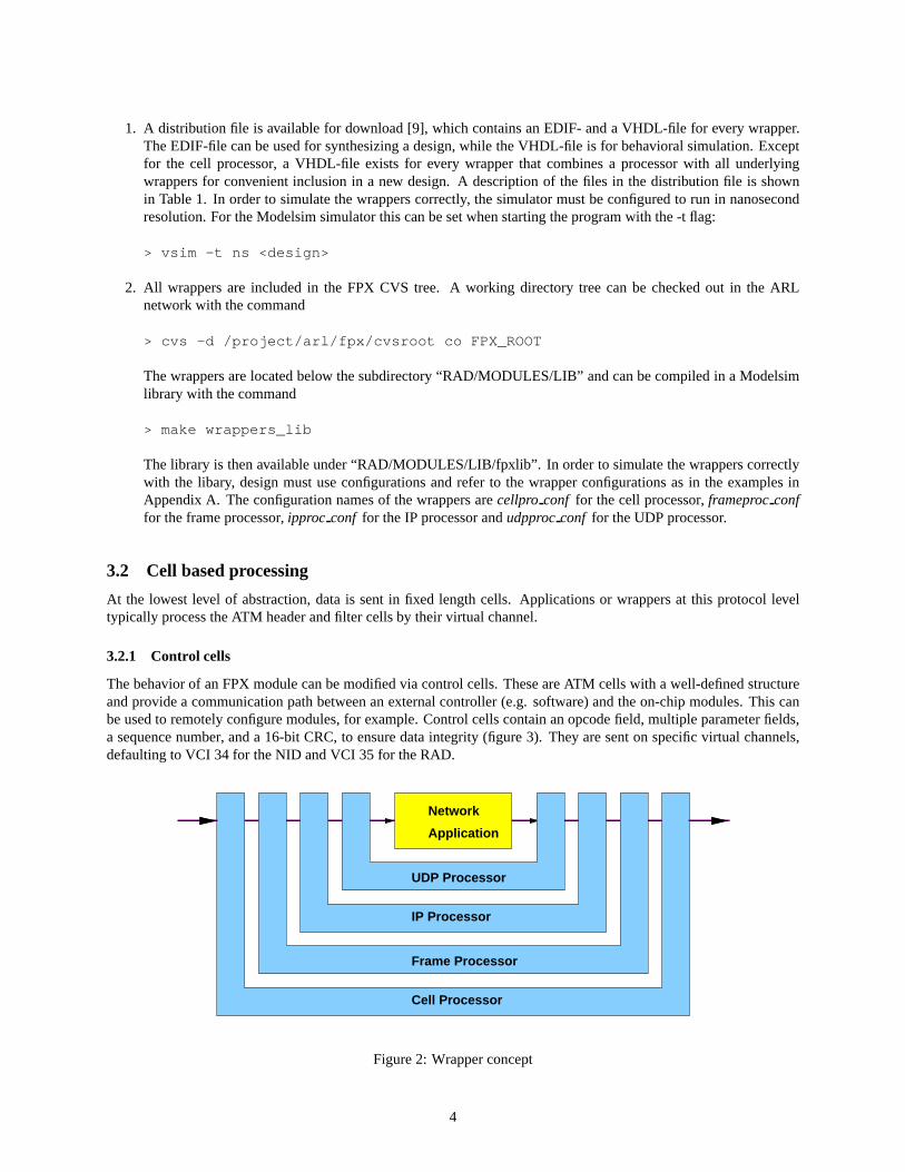
Whenanapplicationmoduleis embeddedinto a protocolwrapper, thenew entity surroundstheuser’s logic likethe letterU (figure2). Regardingthedatastream,theapplicationonly connectsto thetranslatingcomponent,whichwrapsup theapplicationitself. Thereforewe will referto thesurroundingcomponentsaswrappers.
To supporthigher levels of abstraction,the wrapperscanbe nested.Sinceeachhasa well definedinterfaceforan outerandan inner protocol level, they fit togetherwithin eachother, asshown in figure 2. As a result,we get averymodulardesignmethodto supportapplicationsfor differentprotocolsandlevelsof abstraction.Associatingeachwrapperwith a specificprotocol,we geta layermodelcomparableto thewell known OSI/ISOnetworking referencemodel. This modularitygivesapplicationdevelopersfreedomto implementfunctionsat several protocol layersintheir designs.They caninterfacetheir logic to a wrapperwith the level of abstractionappropriatefor their specificapplication.User-level applications,for example,cancompletelyignorehandlingof complicatedprotocolissues,likeframeboundariesor checksums.
3.1 Wrapper Installation
Therearetwo waysto usethewrapperlibrary in aproject.
3
1. A distribution file is availablefor download[9], which containsanEDIF- anda VHDL-file for every wrapper.TheEDIF-file canbeusedfor synthesizinga design,while theVHDL-file is for behavioral simulation.Exceptfor the cell processor, a VHDL-file exists for every wrapperthat combinesa processorwith all underlyingwrappersfor convenientinclusionin a new design. A descriptionof the files in the distribution file is shownin Table1. In orderto simulatethewrapperscorrectly, thesimulatormustbeconfiguredto run in nanosecondresolution.For theModelsimsimulatorthis canbesetwhenstartingtheprogramwith the-t flag:
> vsim -t ns <design>
2. All wrappersare includedin the FPX CVS tree. A working directory tree can be checked out in the ARLnetwork with thecommand
> cvs -d /project/arl/fpx/cvsroot co FPX_ROOT
Thewrappersarelocatedbelow thesubdirectory“RAD/MODULES/LIB” andcanbecompiledin a Modelsimlibrary with thecommand
> make wrappers_lib
Thelibrary is thenavailableunder“RAD/MODULES/LIB/fpxlib”. In orderto simulatethewrapperscorrectlywith the libary, designmustuseconfigurationsandrefer to the wrapperconfigurationsas in the examplesinAppendixA. Theconfigurationnamesof thewrappersarecellpro conf for thecell processor, frameproc conffor theframeprocessor, ipproc conf for theIP processorandudpproc conf for theUDP processor.
3.2 Cell basedprocessing
At the lowest level of abstraction,datais sentin fixed lengthcells. Applicationsor wrappersat this protocol leveltypically processtheATM headerandfilter cellsby their virtual channel.
3.2.1 Control cells
Thebehavior of anFPX modulecanbemodifiedvia controlcells. TheseareATM cellswith a well-definedstructureandprovide a communicationpathbetweenanexternalcontroller(e.g. software)andtheon-chipmodules.This canbeusedto remotelyconfiguremodules,for example.Controlcellscontainanopcodefield, multiple parameterfields,a sequencenumber, anda 16-bit CRC,to ensuredataintegrity (figure3). They aresenton specificvirtual channels,defaultingto VCI 34 for theNID andVCI 35 for theRAD.
UDP Processor
Network
Application
Cell Processor
IP Processor
Frame Processor
Figure2: Wrapperconcept
4
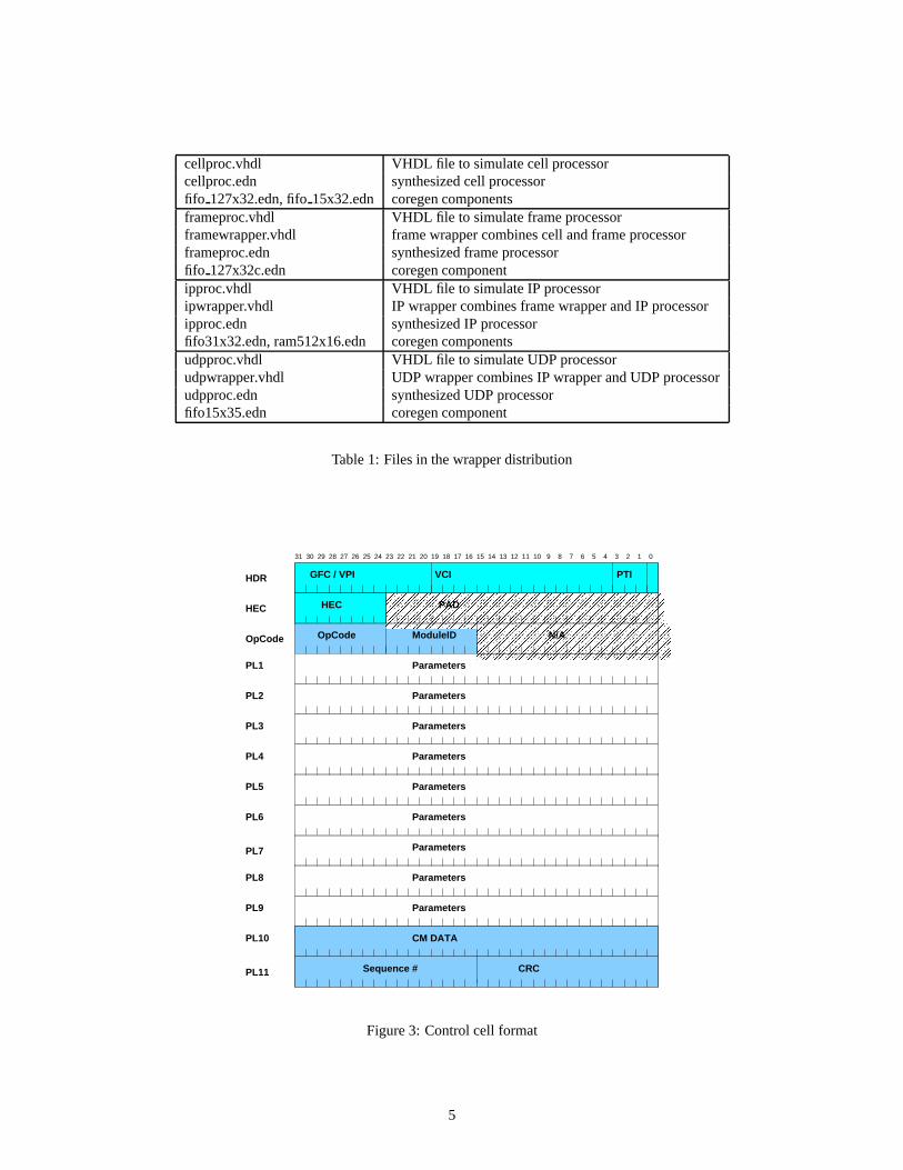
cellproc.vhdl VHDL file to simulatecell processorcellproc.edn synthesizedcell processorfifo 127x32.edn,fifo 15x32.edn coregencomponentsframeproc.vhdl VHDL file to simulateframeprocessorframewrapper.vhdl framewrappercombinescell andframeprocessorframeproc.edn synthesizedframeprocessorfifo 127x32c.edn coregencomponentipproc.vhdl VHDL file to simulateIP processoripwrapper.vhdl IP wrappercombinesframewrapperandIP processoripproc.edn synthesizedIP processorfifo31x32.edn,ram512x16.edn coregencomponentsudpproc.vhdl VHDL file to simulateUDPprocessorudpwrapper.vhdl UDP wrappercombinesIP wrapperandUDP processorudpproc.edn synthesizedUDP processorfifo15x35.edn coregencomponent
Table1: Filesin thewrapperdistribution
DEDEDEDEDEDEDEDEDEDEDEDEDEDEDEDDEDEDEDEDEDEDEDEDEDEDEDEDEDEDEDDEDEDEDEDEDEDEDEDEDEDEDEDEDEDEDFEFEFEFEFEFEFEFEFEFEFEFEFEFEFEFFEFEFEFEFEFEFEFEFEFEFEFEFEFEFEFFEFEFEFEFEFEFEFEFEFEFEFEFEFEFEFGEGEGEGEGEGEGEGEGEGEGEGEGEGEGEGEGEGEGEGEGEGEGGEGEGEGEGEGEGEGEGEGEGEGEGEGEGEGEGEGEGEGEGEGEGGEGEGEGEGEGEGEGEGEGEGEGEGEGEGEGEGEGEGEGEGEGEG
HEHEHEHEHEHEHEHEHEHEHEHEHEHEHEHEHEHEHEHEHEHEHHEHEHEHEHEHEHEHEHEHEHEHEHEHEHEHEHEHEHEHEHEHEHHEHEHEHEHEHEHEHEHEHEHEHEHEHEHEHEHEHEHEHEHEHEH31 30 29 28 27 26 25 24 23 22 21 20 19 18 17 16 15 14 13 12 11 10 9 8 7 6 5 4 3 2 1 0
PL1
PL11
PL10
PL9
PL8
PL7
PL6
PL5
PL4
PL3
PL2
HDR
HEC
OpCode
GFC / VPI VCI
PAD
PTI
Sequence # CRC
HEC
OpCode ModuleID N/A
Parameters
Parameters
Parameters
Parameters
Parameters
Parameters
Parameters
Parameters
Parameters
CM DATA
Figure3: Controlcell format
5
31 30 29 28 27 26 25 24 23 22 21 20 19 18 17 16 15 14 13 12 11 10 9 8 7 6 5 4 3 2 1 0
PL1
PL11
PL10
PL9
PL8
PL7
PL6
PL5
PL4
PL3
PL2
HDR
HEC
OpCode
GFC / VPI VCI
PAD
PTI
Sequence # CRC
HEC
OpCode ModuleID N/A
CM DATA
Control Cell Format for Probe Response
’E’ 0x45 ’x’ 0x78 ’a’ 0x61 ’m’ 0x6d
’p’ 0x70
’p’ 0x70 ’p’ 0x70
’l’ 0x6c ’e’ 0x65
’e’ 0x65
’ ’ 0x20
’ ’ 0x20
’ ’ 0x20
’A’ 0x41 ’l’ 0x6c
’i’ 0x69 ’c’ 0x63 ’a’ 0x61 ’t’ 0x74
’i’ 0x69 ’o’ 0x6f ’n’ 0x6e
’n’ 0x6e’i’ 0x69 ’o’ 0x6f
’V’ 0x56 ’r’ 0x72 ’s’ 0x73
’1’ 0x31 ’.’ 0x2e ’0’ 0x30 ’\0’ 0x00
’\0’ 0x00 ’\0’ 0x00 ’\0’ 0x00 ’\0’ 0x00
Probe Response0x01
0x00 Probe Request (no payload)
OpCode Command
(a)ProbeResponse
31 30 29 28 27 26 25 24 23 22 21 20 19 18 17 16 15 14 13 12 11 10 9 8 7 6 5 4 3 2 1 0
PL1
PL11
PL10
PL9
PL8
PL7
PL6
PL5
PL4
PL3
PL2
HDR
HEC
OpCode
GFC / VPI VCI
PAD
PTI
Sequence # CRC
HEC
V
OpCode ModuleID N/A
Control Cell Format for Setting/Reading VPI/VCI registers
ACreserved (set to zero) Register #
VCIVPI N/A
CM DATA
N/A
N/A
N/AVCI
VCI
VCIVPI
VPI
VPI
V
V
V
C
C
C
A
A
A
reserved (set to zero)
reserved (set to zero)
reserved (set to zero)
Register #
Register #
Register #
N/A
VC − Valid Command
(response only)
Register values:
0x00 Control Cell VPI/VCI
R
R
R
R
RA − Register Available
1 = Valid, 0 = Invalid
1 = valid Reg #, 0 = invalid Reg #
OpCode
0x02 Set VPI/VCI Register
0x03 Set VPI/VCI Register Response
0x04 Read VPI/VCI Register
0x05 Read VPI/VCI Register Response
0x10 default application VPI/VCI
(b) Set/ReadVPI/VCI Registers
Figure4: StandardControlCell Opcodes
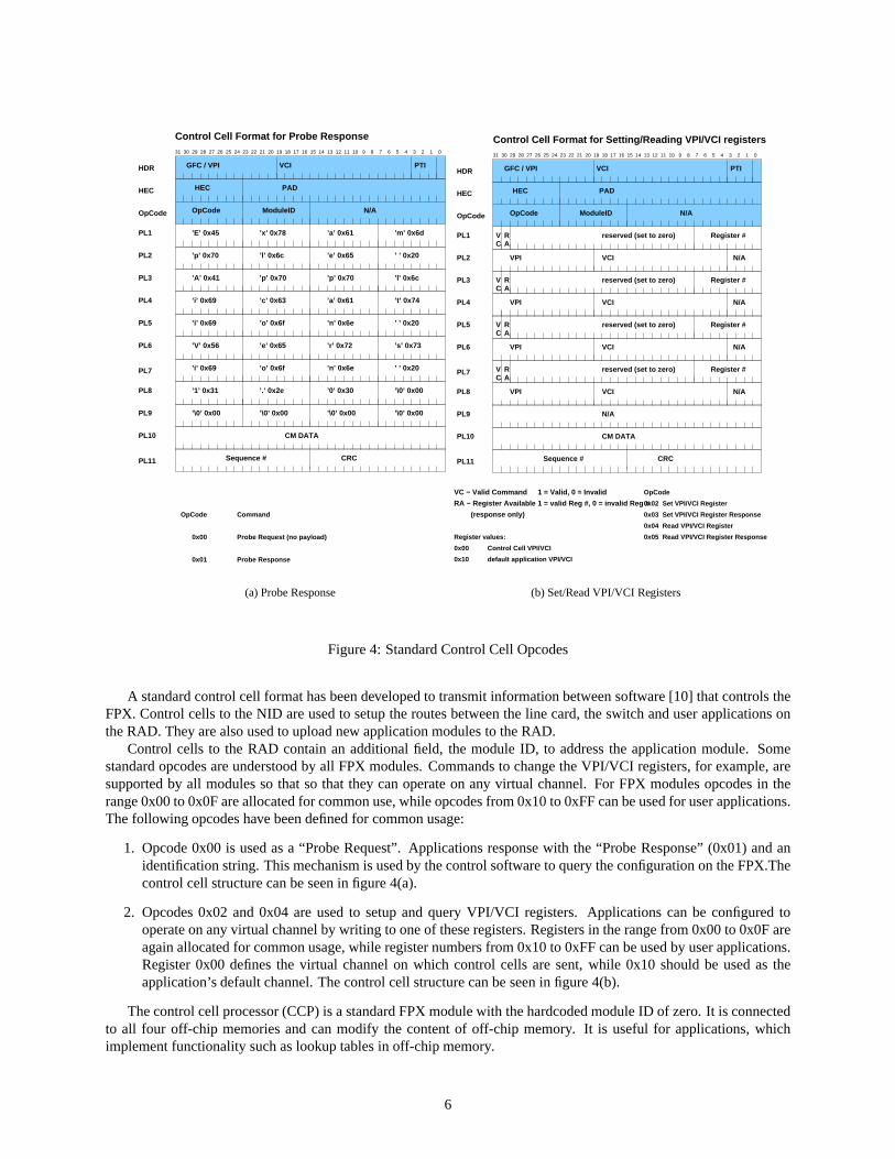
A standardcontrolcell formathasbeendevelopedto transmitinformationbetweensoftware[10] thatcontrolstheFPX.Controlcells to theNID areusedto setuptheroutesbetweenthe line card,theswitchanduserapplicationsontheRAD. They arealsousedto uploadnew applicationmodulesto theRAD.
Control cells to the RAD containan additionalfield, the moduleID, to addressthe applicationmodule. Somestandardopcodesareunderstoodby all FPX modules.Commandsto changetheVPI/VCI registers,for example,aresupportedby all modulesso that so that they canoperateon any virtual channel.For FPX modulesopcodesin therange0x00to 0x0Fareallocatedfor commonuse,while opcodesfrom 0x10to 0xFFcanbeusedfor userapplications.Thefollowing opcodeshavebeendefinedfor commonusage:
1. Opcode0x00 is usedasa “ProbeRequest”.Applicationsresponsewith the “ProbeResponse”(0x01) andanidentificationstring.Thismechanismis usedby thecontrolsoftwareto querytheconfigurationon theFPX.Thecontrolcell structurecanbeseenin figure4(a).
2. Opcodes0x02 and0x04 are usedto setupandquery VPI/VCI registers. Applicationscanbe configuredtooperateonany virtual channelby writing to oneof theseregisters.Registersin therangefrom 0x00to 0x0Fareagainallocatedfor commonusage,while registernumbersfrom 0x10to 0xFFcanbeusedby userapplications.Register0x00 definesthe virtual channelon which control cells aresent,while 0x10 shouldbe usedas theapplication’sdefaultchannel.Thecontrolcell structurecanbeseenin figure4(b).
Thecontrolcell processor(CCP)is astandardFPXmodulewith thehardcodedmoduleID of zero.It is connectedto all four off-chip memoriesandcanmodify the contentof off-chip memory. It is useful for applications,whichimplementfunctionalitysuchaslookuptablesin off-chip memory.
6
Check
Control
Cells
HEC
Set
DispatchHEC
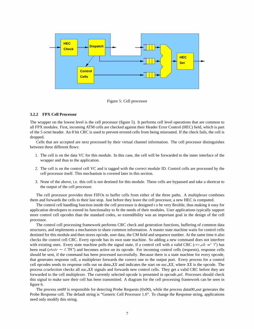
Figure5: Cell processor
3.2.2 FPX Cell Processor
Thewrapperon the lowestlevel is thecell processor(figure5). It performscell level operationsthatarecommontoall FPXmodules.First, incomingATM cellsarecheckedagainsttheirHeaderErrorControl(HEC)field, which is partof the5 octetheader. An 8 bit CRCis usedto preventerroredcellsfrom beingmisrouted.If thecheckfails, thecell isdropped.
Cells thatareacceptedarenext processedby their virtual channelinformation. The cell processordistinguishesbetweenthreedifferentflows:
1. Thecell is on thedataVC for this module.In this case,thecell will be forwardedto the inner interfaceof thewrapperandthusto theapplication.
2. Thecell is on thecontrolcell VC andis taggedwith thecorrectmoduleID. Controlcellsareprocessedby thecell processoritself. Thismechanismis coveredlaterin thissection.
3. Noneof theabove, i.e. this cell is not destinedfor this module.Thesecellsarebypassedandtake a shortcuttotheoutputof thecell processor.
The cell processorprovidesthreeFIFOsto buffer cells from eitherof the threepaths. A multiplexer combinesthemandforwardsthecellsto their laststop.Justbeforethey leave thecell processor, a new HEC is computed.
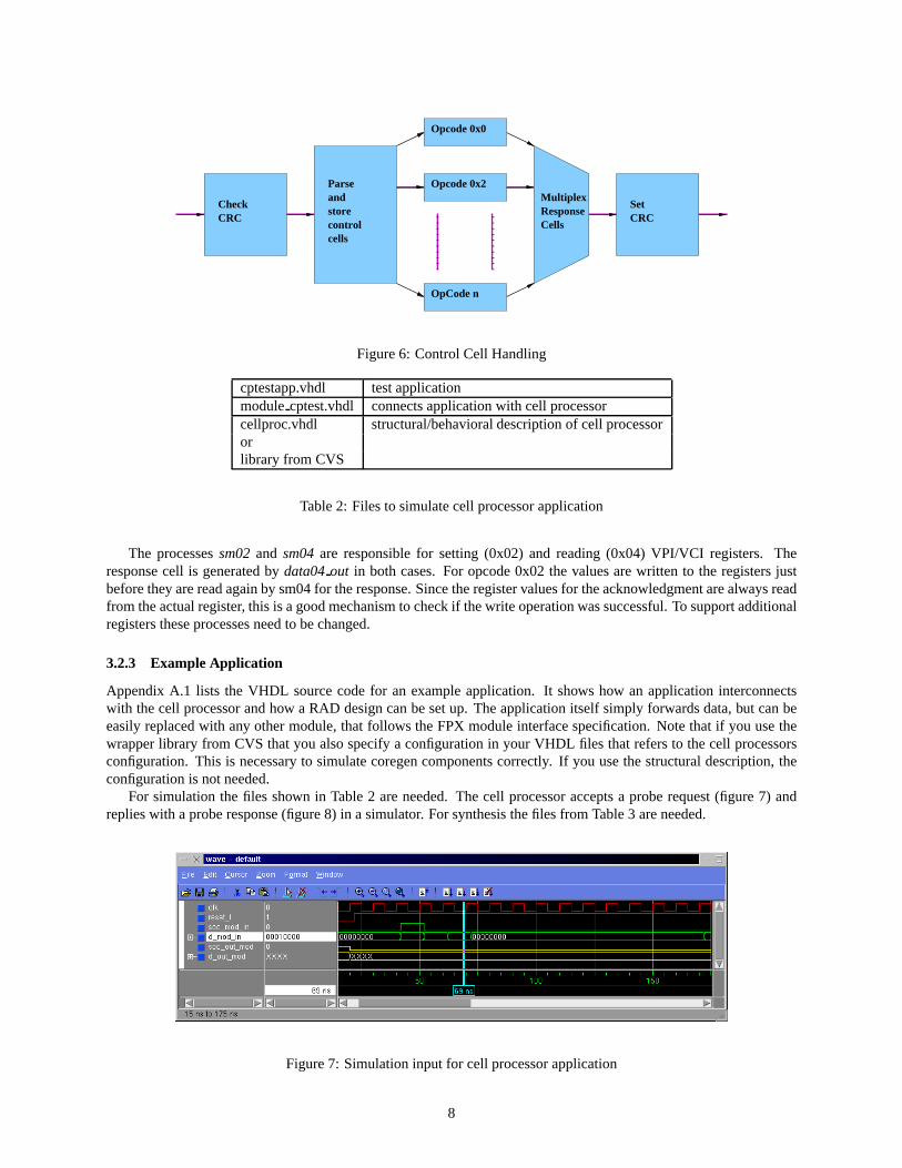
Thecontrolcell handlingfunctioninsidethecell processoris designedt o beveryflexible, thusmakingit easyforapplicationdevelopersto extendits functionalityto fit theneedsof their modules.Userapplicationstypically supportmorecontrol cell opcodesthanthe standardcodes,so extendibility wasan importantgoal in the designof the cellprocessor.
Thecontrolcell processingframework performsCRCcheckandgenerationfunctions,bufferingof commondatastructures,andimplementsamechanismto sharecommoninformation.A masterstatemachinewaitsfor controlcellsdestinedfor thismoduleandthenstoresopcode,userdata,theCM field andsequencenumber. At thesametimeit alsochecksthecontrolcell CRC.Every opcodehasits own statemachine.Soaddinga new commanddoesnot interferewith existing ones.Every statemachinepolls the signalstate, if a control cell with a valid CRC( IKJ"I L.MONQP6RSP ) hasbeenread( TVUXW�UXYZN\[^]_[ ) andbecomesactive on its opcode.For incomingcontrol cells (requests),responsecellsshouldbesent,if thecommandhasbeenprocessedsuccessfully. Becausethereis a statemachinefor every opcode,that generatesresponsecell, a multiplexer forwardsthe correctoneto the outputport. Every processfor a controlcell opcodessendsits responsecellsout on data XX andindicatesthestarton soc XX, whereXX is theopcode.Theprocessccselection checksall soc XX signalsandforwardsnew control cells. They geta valid CRCbeforethey areforwardedto thecell multiplexer. Thecurrentlyselectedopcodeis presentedin opcode sel. Processesshouldcheckthis signalto make suretheir cell hasbeentransmitted.A diagramfor thecell processingframework canbeseeninfigure6.
Theprocesssm00 is responsiblefor detectingProbeRequests(0x00),while theprocessdata00 out generatestheProbeResponsecell. Thedefault stringis “GenericCell Processor1.0”. To changetheResponsestring,applicationsneedonly modify this string.
7
Parseandstore controlcells
MultiplexResponseCells
Opcode 0x0
Opcode 0x2
OpCode n
SetCRC
CheckCRC
Figure6: ControlCell Handling
cptestapp.vhdl testapplicationmodulecptest.vhdl connectsapplicationwith cell processorcellproc.vhdl structural/behavioral descriptionof cell processororlibrary from CVS
Table2: Filesto simulatecell processorapplication
The processessm02 and sm04 are responsiblefor setting(0x02) and reading(0x04) VPI/VCI registers. Theresponsecell is generatedby data04 out in both cases.For opcode0x02 the valuesarewritten to the registersjustbeforethey arereadagainby sm04for theresponse.Sincetheregistervaluesfor theacknowledgmentarealwaysreadfrom theactualregister, this is agoodmechanismto checkif thewrite operationwassuccessful.To supportadditionalregisterstheseprocessesneedto bechanged.
3.2.3 ExampleApplication
AppendixA.1 lists the VHDL sourcecodefor an exampleapplication. It shows how an applicationinterconnectswith thecell processorandhow a RAD designcanbesetup. Theapplicationitself simply forwardsdata,but canbeeasilyreplacedwith any othermodule,that follows theFPX moduleinterfacespecification.Note that if you usethewrapperlibrary from CVS thatyou alsospecifya configurationin your VHDL files that refersto thecell processorsconfiguration.This is necessaryto simulatecoregencomponentscorrectly. If you usethestructuraldescription,theconfigurationis notneeded.
For simulationthe files shown in Table2 areneeded.The cell processoracceptsa proberequest(figure 7) andreplieswith a proberesponse(figure8) in a simulator. For synthesisthefiles from Table3 areneeded.
Figure7: Simulationinput for cell processorapplication
8
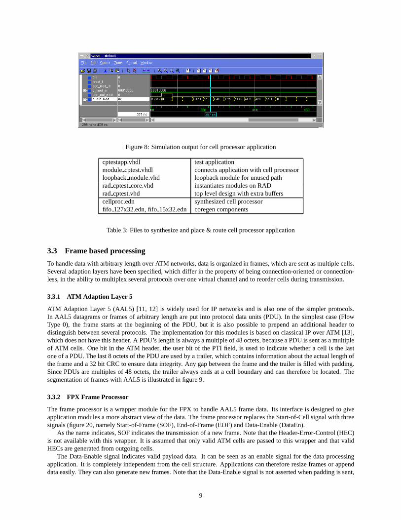
Figure8: Simulationoutputfor cell processorapplication
cptestapp.vhdl testapplicationmodulecptest.vhdl connectsapplicationwith cell processorloopbackmodule.vhd loopbackmodulefor unusedpathrad cptestcore.vhd instantiatesmoduleson RADrad cptest.vhd top level designwith extra bufferscellproc.edn synthesizedcell processorfifo 127x32.edn,fifo 15x32.edn coregencomponents
Table3: Filesto synthesizeandplace& routecell processorapplication
3.3 Frame basedprocessing
To handledatawith arbitrarylengthoverATM networks,datais organizedin frames,whicharesentasmultiplecells.Severaladaptionlayershave beenspecified,which differ in thepropertyof beingconnection-orientedor connection-less,in theability to multiplex severalprotocolsoveronevirtual channelandto reordercellsduringtransmission.
3.3.1 ATM Adaption Layer 5
ATM AdaptionLayer 5 (AAL5) [11, 12] is widely usedfor IP networks and is alsooneof the simplerprotocols.In AAL5 datagramsor framesof arbitrarylengthareput into protocoldataunits (PDU). In the simplestcase(FlowType 0), the frame startsat the beginning of the PDU, but it is also possibleto prependan additionalheadertodistinguishbetweenseveralprotocols.The implementationfor this modulesis basedon classicalIP over ATM [13],whichdoesnothavethisheader. A PDU’s lengthis alwaysamultipleof 48octets,becauseaPDUis sentasamultipleof ATM cells. Onebit in the ATM header, theuserbit of the PTI field, is usedto indicatewhethera cell is the lastoneof aPDU.Thelast8 octetsof thePDUareusedby atrailer, whichcontainsinformationabouttheactuallengthoftheframeanda 32 bit CRCto ensuredataintegrity. Any gapbetweentheframeandthetrailer is filled with padding.SincePDUsaremultiplesof 48 octets,the trailer alwaysendsat a cell boundaryandcanthereforebe located.Thesegmentationof frameswith AAL5 is illustratedin figure9.
3.3.2 FPX Frame Processor
The frameprocessoris a wrappermodulefor the FPX to handleAAL5 framedata. Its interfaceis designedto giveapplicationmodulesamoreabstractview of thedata.TheframeprocessorreplacestheStart-of-Cellsignalwith threesignals(figure20,namelyStart-of-Frame(SOF),End-of-Frame(EOF)andData-Enable(DataEn).
As thenameindicates,SOFindicatesthetransmissionof a new frame.NotethattheHeader-Error-Control(HEC)is not availablewith this wrapper. It is assumedthatonly valid ATM cells arepassedto this wrapperandthat validHECsaregeneratedfrom outgoingcells.
The Data-Enablesignal indicatesvalid payloaddata. It canbe seenasan enablesignalfor the dataprocessingapplication.It is completelyindependentfrom thecell structure.Applicationscanthereforeresizeframesor appenddataeasily. They canalsogeneratenew frames.NotethattheData-Enablesignalis notassertedwhenpaddingis sent,
9
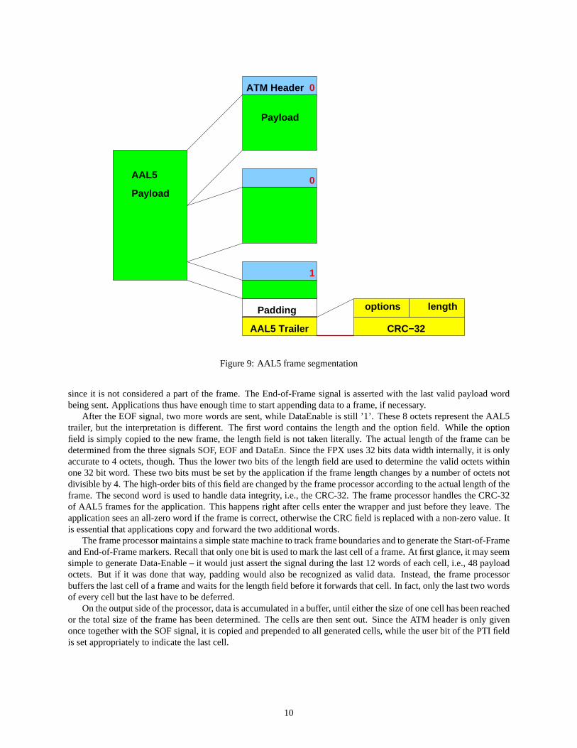
ATM Header
Padding
AAL5 Trailer
Payload
0
0
1
CRC−32
options length
Payload
AAL5
Figure9: AAL5 framesegmentation
sinceit is not considereda part of the frame. The End-of-Framesignalis assertedwith the last valid payloadwordbeingsent.Applicationsthushaveenoughtime to startappendingdatato a frame,if necessary.
After theEOFsignal,two morewordsaresent,while DataEnableis still ’1’. These8 octetsrepresenttheAAL5trailer, but the interpretationis different. The first word containsthe lengthandthe option field. While the optionfield is simply copiedto the new frame,the lengthfield is not taken literally. Theactuallengthof the framecanbedeterminedfrom thethreesignalsSOF, EOFandDataEn.SincetheFPX uses32 bits datawidth internally, it is onlyaccurateto 4 octets,though.Thusthe lower two bits of the lengthfield areusedto determinethevalid octetswithinone32 bit word. Thesetwo bits mustbesetby theapplicationif theframelengthchangesby a numberof octetsnotdivisibleby 4. Thehigh-orderbitsof thisfield arechangedby theframeprocessoraccordingto theactuallengthof theframe. Thesecondword is usedto handledataintegrity, i.e., theCRC-32.TheframeprocessorhandlestheCRC-32of AAL5 framesfor theapplication.This happensright aftercellsenterthewrapperandjust beforethey leave. Theapplicationseesanall-zeroword if theframeis correct,otherwisetheCRCfield is replacedwith a non-zerovalue.Itis essentialthatapplicationscopy andforwardthetwo additionalwords.
Theframeprocessormaintainsasimplestatemachineto trackframeboundariesandto generatetheStart-of-FrameandEnd-of-Framemarkers.Recallthatonly onebit is usedto markthelastcell of aframe.At first glance,it mayseemsimpleto generateData-Enable– it would just assertthesignalduringthelast12 wordsof eachcell, i.e., 48 payloadoctets. But if it wasdonethat way, paddingwould alsobe recognizedasvalid data. Instead,the frameprocessorbuffersthelastcell of a frameandwaitsfor thelengthfield beforeit forwardsthatcell. In fact,only thelasttwo wordsof everycell but thelasthaveto bedeferred.
Ontheoutputsideof theprocessor, datais accumulatedin abuffer, until eitherthesizeof onecell hasbeenreachedor the total sizeof the framehasbeendetermined.Thecellsarethensentout. Sincethe ATM headeris only givenoncetogetherwith theSOFsignal,it is copiedandprependedto all generatedcells,while theuserbit of thePTI fieldis setappropriatelyto indicatethelastcell.
10
`applicationfilesa application
framewrapper.vhdl,moduleframetest.vhdl connectsapplicationwith wrapperscellproc.vhdl,frameproc.vhdl structural/behavioral descriptionof cell andframeprocessorsorlibrary from CVS
Table4: Filesto simulateframebasedapplication
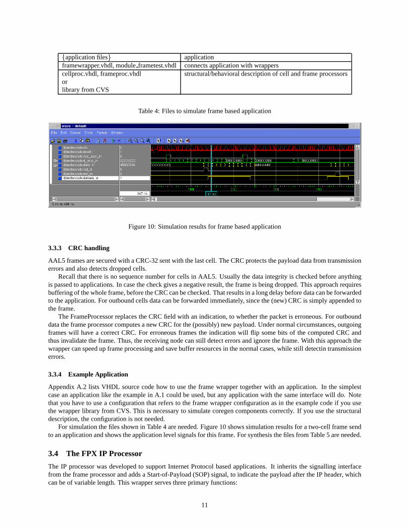
Figure10: Simulationresultsfor framebasedapplication
3.3.3 CRC handling
AAL5 framesaresecuredwith aCRC-32sentwith thelastcell. TheCRCprotectsthepayloaddatafrom transmissionerrorsandalsodetectsdroppedcells.
Recallthat thereis no sequencenumberfor cells in AAL5. Usually thedataintegrity is checkedbeforeanythingis passedto applications.In casethecheckgivesanegativeresult,theframeis beingdropped.Thisapproachrequiresbufferingof thewholeframe,beforetheCRCcanbechecked.Thatresultsin alongdelaybeforedatacanbeforwardedto theapplication.For outboundcellsdatacanbeforwardedimmediately, sincethe(new) CRCis simplyappendedtotheframe.
TheFrameProcessorreplacestheCRCfield with anindication,to whetherthepacket is erroneous.For outbounddatatheframeprocessorcomputesanew CRCfor the(possibly)new payload.Undernormalcircumstances,outgoingframeswill have a correctCRC.For erroneousframesthe indicationwill flip somebits of the computedCRC andthusinvalidatetheframe.Thus,thereceiving nodecanstill detecterrorsandignoretheframe.With this approachthewrappercanspeedupframeprocessingandsavebuffer resourcesin thenormalcases,while still detectintransmissionerrors.
3.3.4 ExampleApplication
AppendixA.2 lists VHDL sourcecodehow to usethe framewrappertogetherwith an application. In the simplestcaseanapplicationlike theexamplein A.1 couldbeused,but any applicationwith thesameinterfacewill do. Notethatyou have to usea configurationthat refersto theframewrapperconfigurationasin theexamplecodeif you usethewrapperlibrary from CVS. This is necessaryto simulatecoregencomponentscorrectly. If you usethestructuraldescription,theconfigurationis not needed.
For simulationthefilesshown in Table4 areneeded.Figure10showssimulationresultsfor a two-cell framesendto anapplicationandshowstheapplicationlevel signalsfor this frame.For synthesisthefilesfrom Table5 areneeded.
3.4 The FPX IP Processor
The IP processorwasdevelopedto supportInternetProtocolbasedapplications.It inherits the signalling interfacefrom theframeprocessorandaddsa Start-of-Payload(SOP)signal,to indicatethepayloadaftertheIP header, whichcanbeof variablelength.This wrapperservesthreeprimaryfunctions:
11
`applicationfilesa application
framewrapper.vhdl connectsthecell processorwith theframeprocessormoduleframetest.vhdl connectsapplicationwith framewrapperloopbackmodule.vhd loopbackmodulefor unusedpathrad frametestcore.vhd instantiatesmoduleson RADrad frametest.vhd top level designwith extrabufferscellproc.edn,frameproc.edn synthesizedcell andframeprocessorsfifo 127x32.edn,fifo 15x32.edn,fifo 127x32c.edn coregencomponents
Table5: Filesto synthesizeandplace& routeframebasedapplication
bQbQbQbQbQbQbQbQbQbQbQbQbQbbQbQbQbQbQbQbQbQbQbQbQbQbQbbQbQbQbQbQbQbQbQbQbQbQbQbQbcQcQcQcQcQcQcQcQcQcQcQcQcQccQcQcQcQcQcQcQcQcQcQcQcQcQccQcQcQcQcQcQcQcQcQcQcQcQcQc
31
31
Update Word 0 Offset
16 15 14
End of Updates Flag
16 15 14 13 12
1
0
2 1 0
Low order address bit0 low order word1 hi order word
AAL5 Trailer
Updates
AAL5 Option EC
Low order Length BitsError Code00 Packet OK11 Error! Drop Packet01, 10 reserved
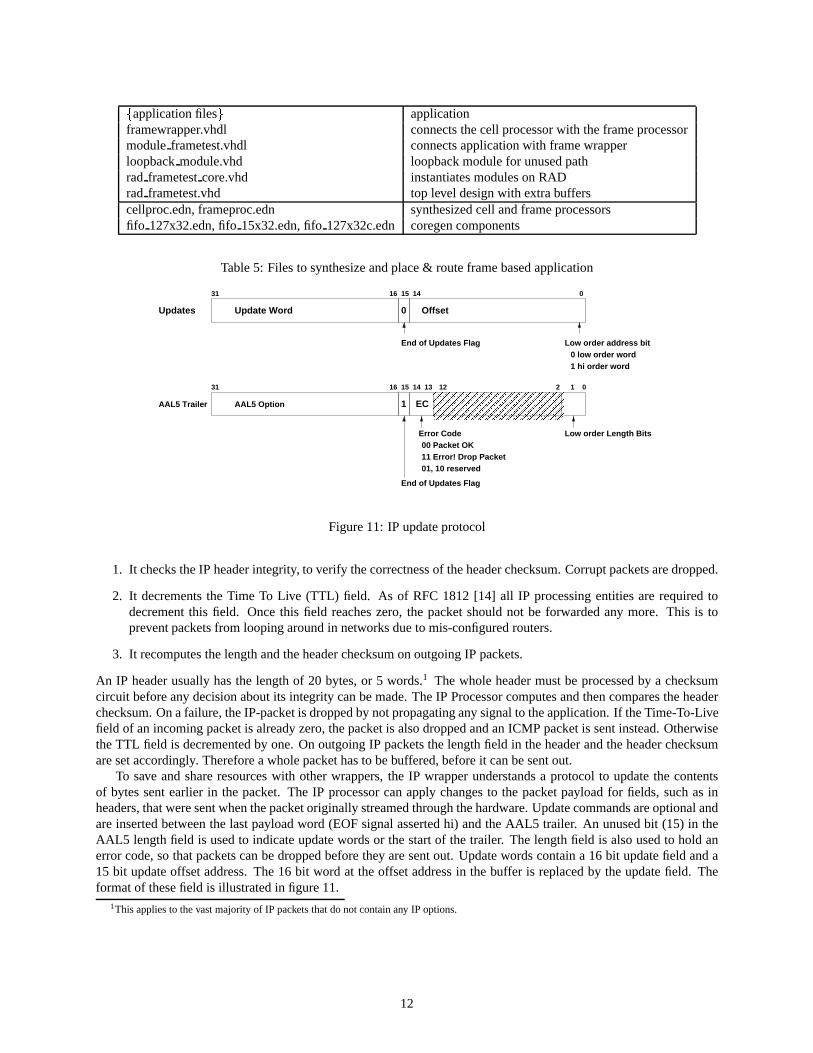
End of Updates Flag
Figure11: IP updateprotocol
1. It checkstheIP headerintegrity, to verify thecorrectnessof theheaderchecksum.Corruptpacketsaredropped.
2. It decrementsthe Time To Live (TTL) field. As of RFC 1812[14] all IP processingentitiesarerequiredtodecrementthis field. Oncethis field reacheszero, the packet shouldnot be forwardedany more. This is topreventpacketsfrom loopingaroundin networksdueto mis-configuredrouters.
3. It recomputesthelengthandtheheaderchecksumonoutgoingIP packets.
An IP headerusuallyhasthe lengthof 20 bytes,or 5 words.1 The wholeheadermustbe processedby a checksumcircuit beforeany decisionaboutits integrity canbemade.TheIP Processorcomputesandthencomparestheheaderchecksum.Onafailure,theIP-packetis droppedby notpropagatingany signalto theapplication.If theTime-To-Livefield of anincomingpacket is alreadyzero,thepacket is alsodroppedandanICMP packet is sentinstead.OtherwisetheTTL field is decrementedby one.On outgoingIP packetsthelengthfield in theheaderandtheheaderchecksumaresetaccordingly. Thereforea wholepackethasto bebuffered,beforeit canbesentout.
To save andshareresourceswith otherwrappers,the IP wrapperunderstandsa protocol to updatethe contentsof bytessentearlier in the packet. The IP processorcanapply changesto the packet payloadfor fields, suchasinheaders,thatweresentwhenthepacketoriginally streamedthroughthehardware.Updatecommandsareoptionalandareinsertedbetweenthe lastpayloadword (EOFsignalassertedhi) andtheAAL5 trailer. An unusedbit (15) in theAAL5 lengthfield is usedto indicateupdatewordsor thestartof the trailer. The lengthfield is alsousedto hold anerrorcode,sothatpacketscanbedroppedbeforethey aresentout. Updatewordscontaina 16 bit updatefield anda15 bit updateoffsetaddress.The16 bit word at theoffsetaddressin the buffer is replacedby theupdatefield. Theformatof thesefield is illustratedin figure11.
1Thisappliesto thevastmajority of IP packetsthatdonotcontainany IP options.
12
`applicationfilesa application
framewrapper.vhdl, ipwrapper.vhdl connectapplicationwith wrappersmoduleiptest.vhdlcellproc.vhdl,frameproc.vhdl,ipproc.vhdl structural/behavioral descriptionof cell, frameandIP processorsorlibrary from CVS
Table6: Filesto simulateIP basedapplication
Figure12: Simulationinput for IP processor
3.4.1 ExampleApplication
AppendixA.3 listsVHDL sourcecodehow to usetheIP wrappertogetherwith anapplication.In thesimplestcaseanapplicationlike theexamplein A.1 couldbeused,but any applicationwith thesameinterfacewill do. Notethatyouhave to usea configurationthat refersto theIP wrapperconfigurationasin theexamplecodeif you usethewrapperlibrary from CVS. This is necessaryto simulatecoregencomponentscorrectly. If you usethestructuraldescription,theconfigurationis not needed.
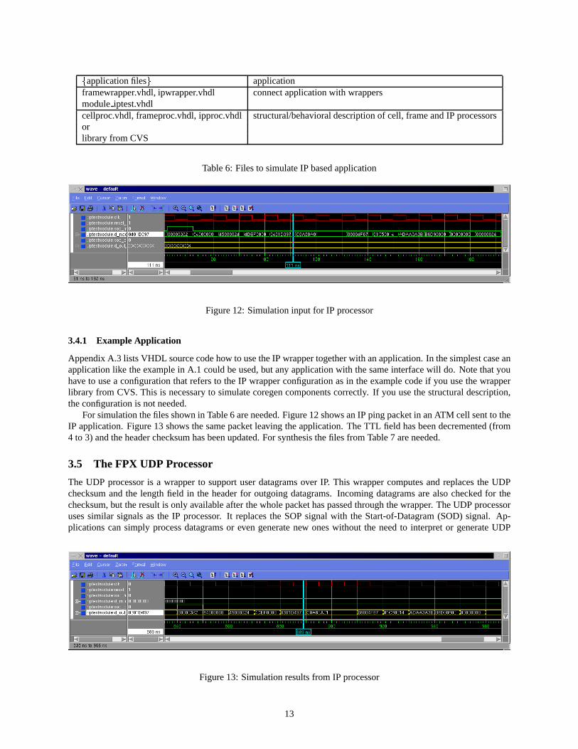
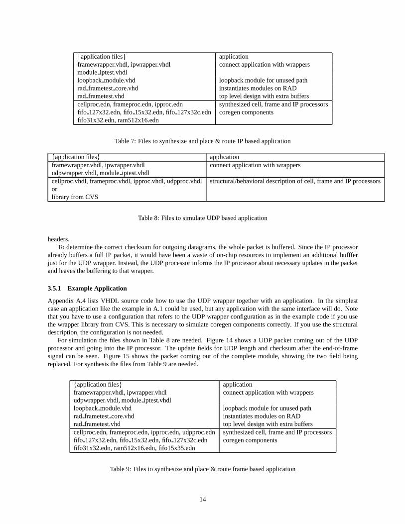
For simulationthefilesshown in Table6 areneeded.Figure12showsanIP pingpacket in anATM cell sentto theIP application.Figure13 shows thesamepacket leaving theapplication.TheTTL field hasbeendecremented(from4 to 3) andtheheaderchecksumhasbeenupdated.For synthesisthefiles from Table7 areneeded.
3.5 The FPX UDP Processor
The UDP processoris a wrapperto supportuserdatagramsover IP. This wrappercomputesandreplacesthe UDPchecksumandthe lengthfield in the headerfor outgoingdatagrams.Incomingdatagramsarealsochecked for thechecksum,but theresultis only availableafterthewholepackethaspassedthroughthewrapper. TheUDP processorusessimilar signalsasthe IP processor. It replacesthe SOPsignalwith the Start-of-Datagram(SOD) signal. Ap-plicationscansimply processdatagramsor even generatenew oneswithout the needto interpretor generateUDP
Figure13: Simulationresultsfrom IP processor
13
`applicationfilesa application
framewrapper.vhdl, ipwrapper.vhdl connectapplicationwith wrappersmoduleiptest.vhdlloopbackmodule.vhd loopbackmodulefor unusedpathrad frametestcore.vhd instantiatesmoduleson RADrad frametest.vhd top level designwith extra bufferscellproc.edn,frameproc.edn,ipproc.edn synthesizedcell, frameandIP processorsfifo 127x32.edn,fifo 15x32.edn,fifo 127x32c.edn coregencomponentsfifo31x32.edn,ram512x16.edn
Table7: Filesto synthesizeandplace& routeIP basedapplication
`applicationfilesa application
framewrapper.vhdl, ipwrapper.vhdl connectapplicationwith wrappersudpwrapper.vhdl,moduleiptest.vhdlcellproc.vhdl,frameproc.vhdl,ipproc.vhdl,udpproc.vhdl structural/behavioral descriptionof cell, frameandIP processorsorlibrary from CVS
Table8: Filesto simulateUDP basedapplication
headers.To determinethecorrectchecksumfor outgoingdatagrams,thewholepacket is buffered. SincetheIP processor
alreadybuffersa full IP packet, it would have beena wasteof on-chipresourcesto implementan additionalbuffferjust for theUDP wrapper. Instead,theUDP processorinformstheIP processoraboutnecessaryupdatesin thepacketandleavesthebuffering to thatwrapper.
3.5.1 ExampleApplication
AppendixA.4 lists VHDL sourcecodehow to usethe UDP wrappertogetherwith an application. In the simplestcaseanapplicationlike theexamplein A.1 couldbeused,but any applicationwith thesameinterfacewill do. Notethatyou have to usea configurationthat refersto the UDP wrapperconfigurationasin theexamplecodeif you usethewrapperlibrary from CVS. This is necessaryto simulatecoregencomponentscorrectly. If you usethestructuraldescription,theconfigurationis not needed.
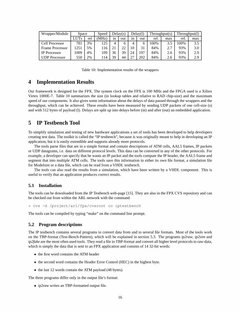
For simulationthe files shown in Table8 areneeded.Figure14 shows a UDP packet comingout of the UDPprocessorandgoing into the IP processor. The updatefields for UDP lengthandchecksumafter the end-of-framesignal canbe seen. Figure 15 shows the packet comingout of the completemodule,showing the two field beingreplaced.For synthesisthefiles from Table9 areneeded.
`applicationfilesa application
framewrapper.vhdl, ipwrapper.vhdl connectapplicationwith wrappersudpwrapper.vhdl,moduleiptest.vhdlloopbackmodule.vhd loopbackmodulefor unusedpathrad frametestcore.vhd instantiatesmoduleson RADrad frametest.vhd top level designwith extrabufferscellproc.edn,frameproc.edn,ipproc.edn,udpproc.edn synthesizedcell, frameandIP processorsfifo 127x32.edn,fifo 15x32.edn,fifo 127x32c.edn coregencomponentsfifo31x32.edn,ram512x16.edn,fifo15x35.edn
Table9: Filesto synthesizeandplace& routeframebasedapplication
14
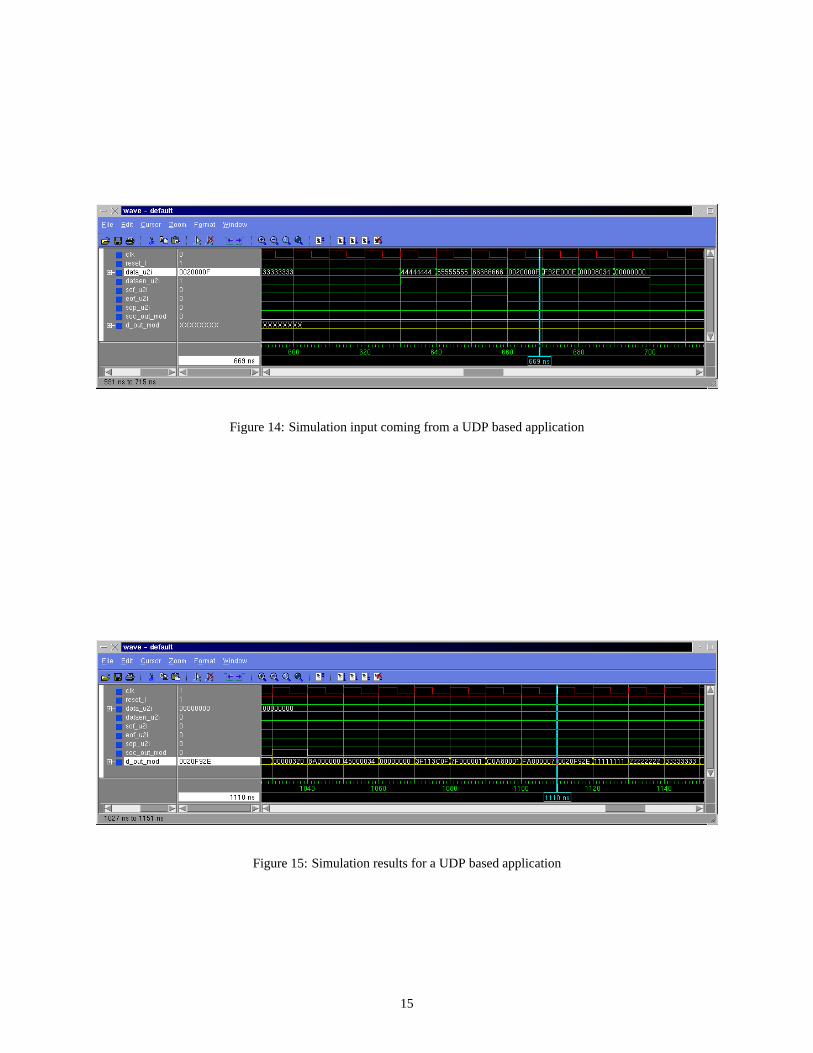
Figure14: Simulationinputcomingfrom a UDP basedapplication
Figure15: Simulationresultsfor a UDP basedapplication
15
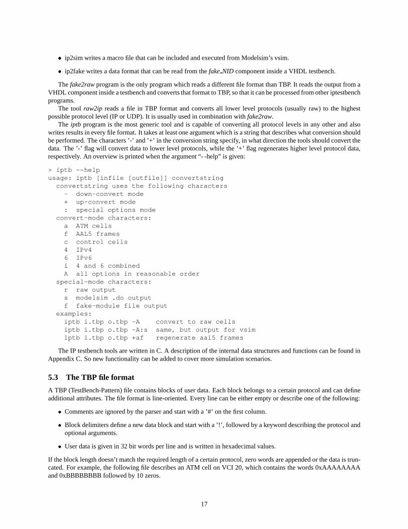
Wrapper/Module Space Speed Delay(s) Delay(l) Throughput(s) Throughput(l)LUTs rel (MHz) in out in out rel. max rel. max
Cell Processor 781 3% 125 4 6 4 6 100% 3.5 100% 3.5FrameProcessor 1251 5% 116 21 22 10 31 84% 2.7 93% 3.0IP Processor 1009 4% 109 36 39 24 197 84% 2.6 93% 2.9UDP Processor 550 2% 114 39 44 27 202 84% 2.6 93% 2.9
Table10: Implementationresultsof thewrappers
4 Implementation Results
Our framework is designedfor the FPX. The systemclock on the FPX is 100 MHz andthe FPGA usedis a XilinxVirtex 1000E-7. Table10 summarizesthe size(in lookup tablesandrelative to RAD chip-size)andthe maximumspeedof ourcomponents.It alsogivessomeinformationaboutthedelaysof datapassedthroughthewrappersandthethroughput,which canbe achieved. Theseresultshave beenmeasuredby sendingUDP packetsof onecell-size(s)andwith 512bytesof payload(l). Delaysaresplit up into delaysbefore(in) andafter(out)anembeddedapplication.
5 IP TestbenchTool
To simplify simulationandtestingof new hardwareapplicationsa setof toolshasbeendevelopedto helpdeveloperscreatingtestdata.Thetoolkit is calledthe“IP testbench”,becauseis wasoriginally meantto helpin developinganIPapplication,but it is easilyextendibleandsupportsalreadymoreprotocols.
Thetoolsparsefiles thatarein a simpleformatandcontaindescriptionsof ATM cells,AAL5 frames,IP packetsor UDP datagrams,i.e. dataon differentprotocollevels.This datacanbeconvertedin any of theotherprotocols.Forexample,adevelopercanspecifythathewantsanIP packetandthetoolscomputetheIP header, theAAL5 frameandsegmentthat into multiple ATM cells. Thetools save this informationin eitherits own file format,a simulationfilefor Modelsimor a datafile, which canbereadfrom aVHDL testbench.
The tools canalsoreadthe resultsfrom a simulation,which have beenwritten by a VHDL component.This isusefulto verify thatanapplicationproducescorrectresults.
5.1 Installation
Thetoolscanbedownloadedfrom theIP Testbenchweb-page[15]. They arealsoin theFPXCVSrepositoryandcanbecheckedout from within theARL network with thecommand
> cvs -d /project/arl/fpx/cvsroot co iptestbench
Thetoolscanbecompiledby typing “make” on thecommandline prompt.
5.2 Program descriptions
The IP testbenchcontainsseveralprogramsto convert datafrom andto severalfile formats. Most of the toolsworkon the TBP-format(Test-Bench-Pattern),which will be explainedin section5.3. The programsip2raw, ip2sim andip2fake arethemostoftenusedtools.They readafile in TBP-formatandconvertall higherlevel protocolsto raw-data,which is simply thedatathatis sentto anFPX applicationandconsistsof 14 32-bitwords:
d thefirst wordcontainstheATM header
d thesecondword containstheHeaderErrorControl(HEC) in thehighestbyte.
d thelast12 wordscontaintheATM payload(48 bytes).
Thethreeprogramsdiffer only in theoutputfile’s format:
d ip2raw writesanTBP-formattedoutputfile.
16
d ip2simwritesa macrofile thatcanbeincludedandexecutedfrom Modelsim’svsim.
d ip2fakewritesa dataformatthatcanbereadfrom thefake NID componentinsidea VHDL testbench.
Thefake2raw programis theonly programwhich readsadifferentfile formatthanTBP. It readstheoutputfrom aVHDL componentinsideatestbenchandconvertsthatformatto TBP, sothatit canbeprocessedfromotheriptestbenchprograms.
The tool raw2ip readsa file in TBP format andconvertsall lower level protocols(usually raw) to the highestpossibleprotocollevel (IP or UDP). It is usuallyusedin combinationwith fake2raw.
The iptb programis the mostgenerictool andis capableof convertingall protocol levels in any otherandalsowritesresultsin everyfile format. It takesat leastoneargumentwhichis astringthatdescribeswhatconversionshouldbeperformed.Thecharacters’-’ and’+’ in theconversionstringspecify, in whatdirectionthetoolsshouldconvert thedata.The ’-’ flag will convert datato lower level protocols,while the ’+’ flag regenerateshigherlevel protocoldata,respectively. An overview is printedwhentheargument“- -help” is given:
> iptb --helpusage: iptb [infile [outfile]] convertstring
convertstring uses the following characters- down-convert mode+ up-convert mode: special options mode
convert-mode characters:a ATM cellsf AAL5 framesc control cells4 IPv46 IPv6i 4 and 6 combinedA all options in reasonable order
special-mode characters:r raw outputs modelsim .do outputf fake-module file output
examples:iptb i.tbp o.tbp -A convert to raw cellsiptb i.tbp o.tbp -A:s same, but output for vsimiptb i.tbp o.tbp +af regenerate aal5 frames
TheIP testbenchtoolsarewritten in C. A descriptionof theinternaldatastructuresandfunctionscanbefoundinAppendixC. Sonew functionalitycanbeaddedto covermoresimulationscenarios.
5.3 The TBP file format
A TBP (TestBench-Pattern)file containsblocksof userdata.Eachblock belongsto a certainprotocolandcandefineadditionalattributes.Thefile formatis line-oriented.Every line canbeeitheremptyor describeoneof thefollowing:
d Commentsareignoredby theparserandstartwith a ’#’ on thefirst column.
d Block delimitersdefineanew datablockandstartwith a ’!’, followedby akeyworddescribingtheprotocolandoptionalarguments.
d Userdatais givenin 32bit wordsperline andis written in hexadecimalvalues.
If theblock lengthdoesn’t matchtherequiredlengthof acertainprotocol,zerowordsareappendedor thedatais trun-cated.For example,thefollowing file describesanATM cell on VCI 20, which containsthewords0xAAAAAAAAand0xBBBBBBBB followedby 10 zeros.
17
# example for an ATM cell!CELL 20aaaaaaaabbbbbbbb
A descriptionof all definedblock typesis givenbelow, includinga descriptionof theoptionalarguments.
PAD is usedto insertbreaksbetweenblocksfor simulation. The argumentspecifiesthe numberof clock cyclestowait, i.e. multiplesof 10ns.
RAW is usedto senta raw block of datato an application. The simulatorwill give an SOCsignalfollowedby theRAW datablock. Thefirst wordusuallydefinestheATM header, thesecondcontainstheHeaderErrorControl(HEC)in thehighestbyte.RAW hasno additionalarguments.
CELL definesanATM cell. Thedatablockwill beusedastheCELL payload.It is expandedor truncatedto 12words,if thedatablock hasa differentlength.This block typeacceptstwo arguments.Thefirst definestheVCI, thesecondis a flag whetherthe PTI field shouldbe set(endof AAL5-frame marker). CELL blocksareconvertedto RAW byprecedinganATM headeranda HEC.
CTRLCELL definesacontrolcell asit is usedto configureFPXmodules.It acceptsthreearguments:theopcode,themoduleID andthecontrolcell VCI. CTRLCELL blocksareconvertedto CELL by generatingthecontrolcell header,a sequencenumber, andtheCRC.
FRAME definesanAAL5 frame.TheVCI canbegivenasanargument.FRAME blocksareconvertedto (multiple)cellsby generatinga AAL5-PDU, appendingpadding,thelengthfield antheCRC.
IPv4 is usedto specify IP version4 packets. It acceptsup to four arguments:the destinationIP address(in dottedquadnotation),theprotocolnumber, theTTL valueandtheVCI. IPv4packetsareconvertedto FRAME by precedingtheIP version4 header, includingthelengthfield andthechecksum.
UDP is usedto sentUDP datagrams.ThedestinationIP addressandthedestinationandsourceport canbespecifiedasarguments.UDPis convertedto IPv4with theprotocolnumber7 by precedingaUDPheader, includinglengthfieldanchecksum,to thepayload.
6 Conclusions
We have presenteda framework for IP packet processingapplicationsin hardware. Althoughour currentimplemen-tationwascreatedfor usein theField ProgrammablePortExtender, theframework is very generalandcaneasilybeadaptedto otherplatforms.A library of LayeredProtocolwrappershasbeenimplemented.Eachhandlesa particularprotocol level. By usingan entity that surroundsan applicationmodule(a U-shapewrapper),the relatedlogic toconvert to andfrom a protocolarelinked, increasingtheflexibility andreducingthe numberof cross-dependencies.Thecommoninterfacebetweenlayersalsolowersthelearningcurve.
Theframework is usefulfor developersof networkinghardwarecomponents.Applicationsthemselvesdon’t haveto take careaboutnetwork protocol issues.The completeIP processingframework only utilizes 14% of the RADFPGAon theFPX, leaving sufficient spaceto implementuser-definedlogic.
18
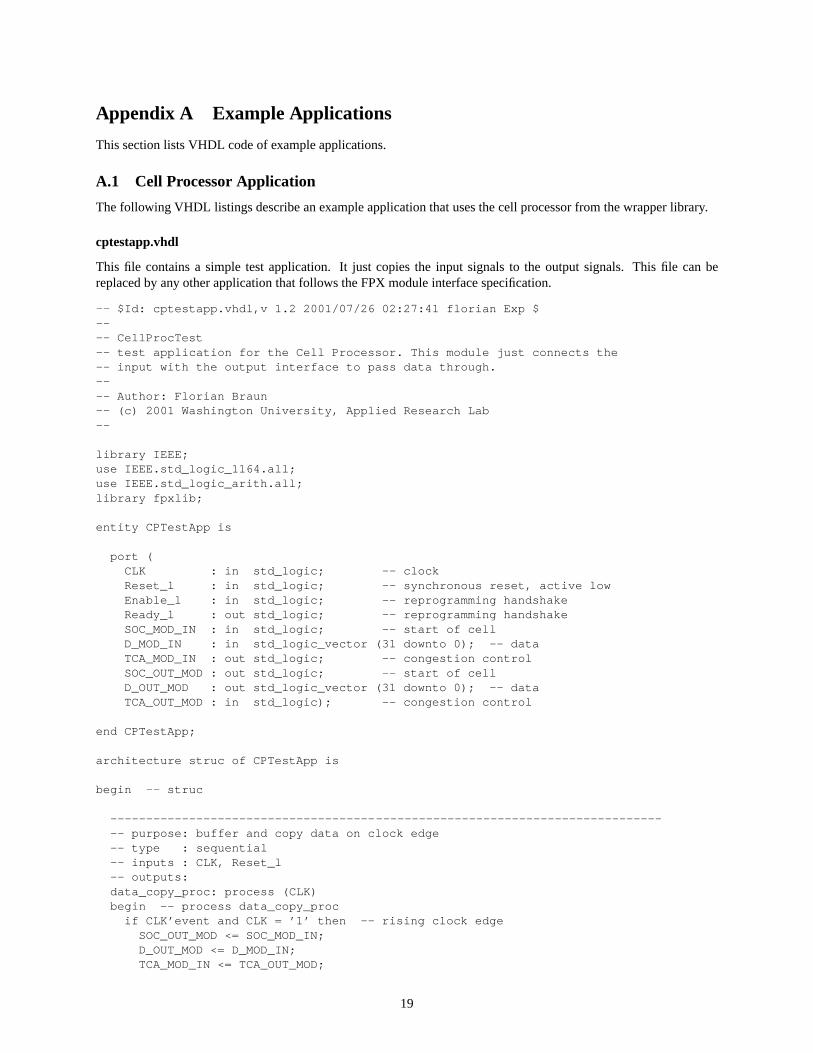
Appendix A Example Applications
Thissectionlists VHDL codeof exampleapplications.
A.1 Cell ProcessorApplication
Thefollowing VHDL listingsdescribeanexampleapplicationthatusesthecell processorfrom thewrapperlibrary.
cptestapp.vhdl
This file containsa simple testapplication. It just copiesthe input signalsto the outputsignals. This file canbereplacedby any otherapplicationthatfollows theFPX moduleinterfacespecification.
-- $Id: cptestapp.vhdl,v 1.2 2001/07/26 02:27:41 florian Exp $---- CellProcTest-- test application for the Cell Processor. This module just connects the-- input with the output interface to pass data through.---- Author: Florian Braun-- (c) 2001 Washington University, Applied Research Lab--
library IEEE;use IEEE.std_logic_1164.all;use IEEE.std_logic_arith.all;library fpxlib;
entity CPTestApp is
port (CLK : in std_logic; -- clockReset_l : in std_logic; -- synchronous reset, active lowEnable_l : in std_logic; -- reprogramming handshakeReady_l : out std_logic; -- reprogramming handshakeSOC_MOD_IN : in std_logic; -- start of cellD_MOD_IN : in std_logic_vector (31 downto 0); -- dataTCA_MOD_IN : out std_logic; -- congestion controlSOC_OUT_MOD : out std_logic; -- start of cellD_OUT_MOD : out std_logic_vector (31 downto 0); -- dataTCA_OUT_MOD : in std_logic); -- congestion control
end CPTestApp;
architecture struc of CPTestApp is
begin -- struc
------------------------------------------------------------------------------- purpose: buffer and copy data on clock edge-- type : sequential-- inputs : CLK, Reset_l-- outputs:data_copy_proc: process (CLK)begin -- process data_copy_procif CLK’event and CLK = ’1’ then -- rising clock edge
SOC_OUT_MOD <= SOC_MOD_IN;D_OUT_MOD <= D_MOD_IN;TCA_MOD_IN <= TCA_OUT_MOD;
19
Ready_l <= not Enable_l;end if;
end process data_copy_proc;
end struc;
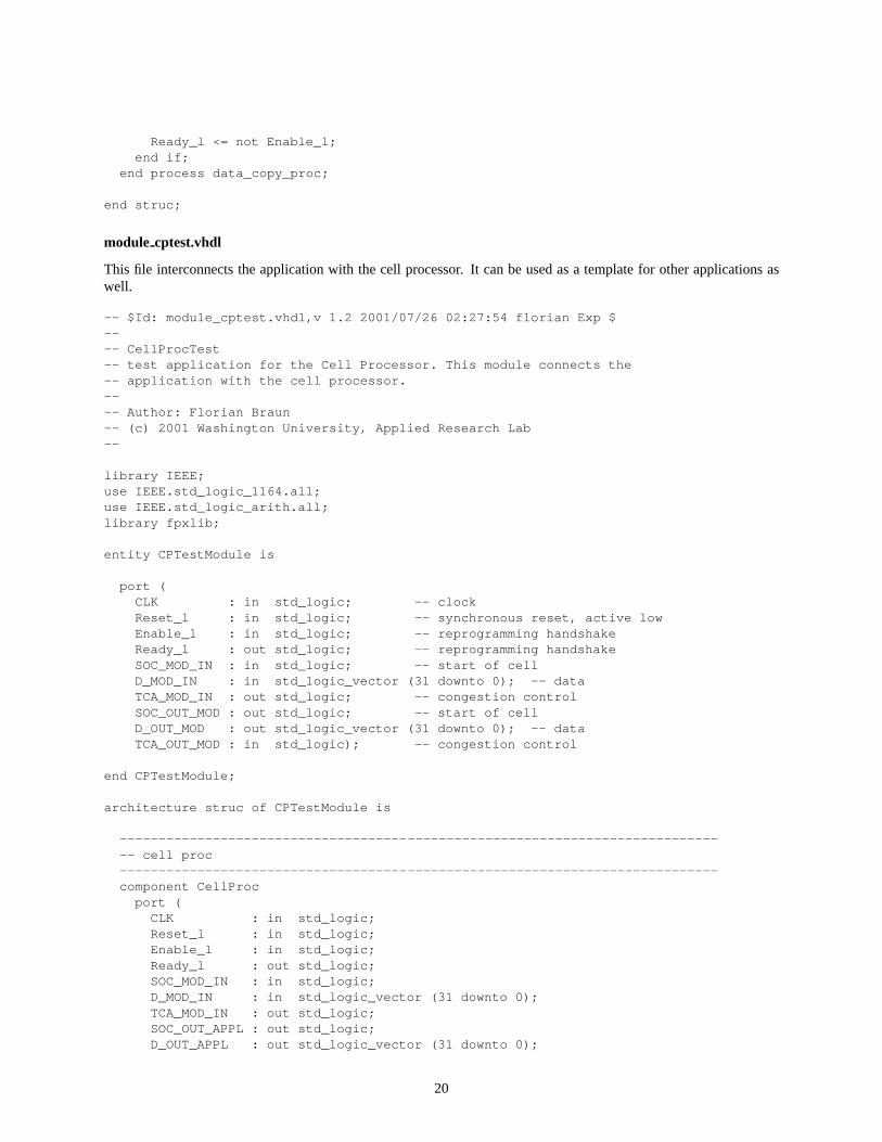
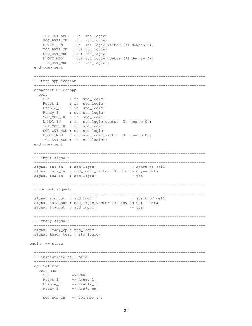
module cptest.vhdl
This file interconnectsthe applicationwith the cell processor. It canbe usedasa templatefor otherapplicationsaswell.
-- $Id: module_cptest.vhdl,v 1.2 2001/07/26 02:27:54 florian Exp $---- CellProcTest-- test application for the Cell Processor. This module connects the-- application with the cell processor.---- Author: Florian Braun-- (c) 2001 Washington University, Applied Research Lab--
library IEEE;use IEEE.std_logic_1164.all;use IEEE.std_logic_arith.all;library fpxlib;
entity CPTestModule is
port (CLK : in std_logic; -- clockReset_l : in std_logic; -- synchronous reset, active lowEnable_l : in std_logic; -- reprogramming handshakeReady_l : out std_logic; -- reprogramming handshakeSOC_MOD_IN : in std_logic; -- start of cellD_MOD_IN : in std_logic_vector (31 downto 0); -- dataTCA_MOD_IN : out std_logic; -- congestion controlSOC_OUT_MOD : out std_logic; -- start of cellD_OUT_MOD : out std_logic_vector (31 downto 0); -- dataTCA_OUT_MOD : in std_logic); -- congestion control
end CPTestModule;
architecture struc of CPTestModule is
------------------------------------------------------------------------------- cell proc-----------------------------------------------------------------------------component CellProcport (
CLK : in std_logic;Reset_l : in std_logic;Enable_l : in std_logic;Ready_l : out std_logic;SOC_MOD_IN : in std_logic;D_MOD_IN : in std_logic_vector (31 downto 0);TCA_MOD_IN : out std_logic;SOC_OUT_APPL : out std_logic;D_OUT_APPL : out std_logic_vector (31 downto 0);
20
TCA_OUT_APPL : in std_logic;SOC_APPL_IN : in std_logic;D_APPL_IN : in std_logic_vector (31 downto 0);TCA_APPL_IN : out std_logic;SOC_OUT_MOD : out std_logic;D_OUT_MOD : out std_logic_vector (31 downto 0);TCA_OUT_MOD : in std_logic);
end component;
------------------------------------------------------------------------------- test application-----------------------------------------------------------------------------component CPTestAppport (
CLK : in std_logic;Reset_l : in std_logic;Enable_l : in std_logic;Ready_l : out std_logic;SOC_MOD_IN : in std_logic;D_MOD_IN : in std_logic_vector (31 downto 0);TCA_MOD_IN : out std_logic;SOC_OUT_MOD : out std_logic;D_OUT_MOD : out std_logic_vector (31 downto 0);TCA_OUT_MOD : in std_logic);
end component;
------------------------------------------------------------------------------- input signals-----------------------------------------------------------------------------signal soc_in : std_logic; -- start of cellsignal data_in : std_logic_vector (31 downto 0);-- datasignal tca_in : std_logic; -- tca
------------------------------------------------------------------------------- output signals-----------------------------------------------------------------------------signal soc_out : std_logic; -- start of cellsignal data_out : std_logic_vector (31 downto 0);-- datasignal tca_out : std_logic; -- tca
------------------------------------------------------------------------------- ready signals-----------------------------------------------------------------------------signal Ready_cp : std_logic;signal Ready_test : std_logic;
begin -- struc
------------------------------------------------------------------------------- instantiate cell proc-----------------------------------------------------------------------------cp: CellProcport map (
CLK => CLK,Reset_l => Reset_l,Enable_l => Enable_l,Ready_l => Ready_cp,
SOC_MOD_IN => SOC_MOD_IN,
21
D_MOD_IN => D_MOD_IN,TCA_MOD_IN => TCA_MOD_IN,
SOC_OUT_APPL => soc_in,D_OUT_APPL => data_in,TCA_OUT_APPL => tca_in,
SOC_APPL_IN => soc_out,D_APPL_IN => data_out,TCA_APPL_IN => tca_out,
SOC_OUT_MOD => SOC_OUT_MOD,D_OUT_MOD => D_OUT_MOD,TCA_OUT_MOD => TCA_OUT_MOD);
------------------------------------------------------------------------------- instantiate test application-----------------------------------------------------------------------------test: CPTestAppport map (
CLK => CLK,Reset_l => Reset_l,Enable_l => Enable_l,Ready_l => Ready_test,SOC_MOD_IN => soc_in,D_MOD_IN => data_in,TCA_MOD_IN => tca_in,SOC_OUT_MOD => soc_out,D_OUT_MOD => data_out,TCA_OUT_MOD => tca_out);
------------------------------------------------------------------------------- misc connections-----------------------------------------------------------------------------Ready_l <= not (Ready_cp and Ready_test);
end struc;
configuration cptest_conf of CPTestModule is
for struc
for all : CellProcuse configuration fpxlib.cellproc_conf;
end for;
end for;
end cptest_conf;
loopback module.vhdl
This modulejust connectsthe input signalswith theoutputsignalsandis usedto passdatathroughtheunusedpathon theRAD.
-- Applied Research Laboratory-- Washington University in St. Louis---- File: loopback_module.vhd
22
-- Entity declaration for RAD module-- Created by: David E. Taylor ([email protected])-- Created on: August, 16 2000-- Last modified: August 18, 2000 @ 11:20 am---- IMPORTANT: Refer to RAD Module Interface Specification-- for explanations and timing specifications for all interface-- signals.--library IEEE;use IEEE.STD_LOGIC_1164.all;--ENTITY loopback_module IS
PORT (-- Clock & Resetclk : in STD_LOGIC; -- 100MHz global clockreset_l : in STD_LOGIC; -- Synchronous reset, asserted-low
-- Cell Input Interfacesoc_mod_in : in STD_LOGIC; -- Start of celld_mod_in : in STD_LOGIC_VECTOR(31 downto 0); -- 32-bit datatca_mod_in : out STD_LOGIC; -- Transmit cell available
-- Cell Output Interfacesoc_out_mod : out STD_LOGIC; -- Start of celld_out_mod : out STD_LOGIC_VECTOR(31 downto 0); -- 32-bit datatca_out_mod : in STD_LOGIC; -- Transmit cell availabletest_data : out STD_LOGIC_VECTOR(31 downto 0) -- 32-bit data);
end loopback_module;
architecture behavioral of loopback_module is
signal soc : std_logic; -- Start of Cellsignal data : std_logic_vector(31 downto 0); -- 32-bit words of ATM cellsignal tca : std_logic; -- Transmit Cell Available
--begin -- behavioral---- Pass cells through. On reconfig, hold TCA low.--
CELL_IO_FF : process (clk)begin -- process CELL_FFif (clk=’1’ and clk’event) then
if reset_l=’0’ thensoc <= ’0’;soc_out_mod <= ’0’;data <= (others=>’0’) ;d_out_mod <= (others=>’0’) ;tca <= ’0’ ;tca_mod_in <= ’0’ ;
elsesoc <= soc_mod_in ;data <= d_mod_in ;soc_out_mod <= soc ;d_out_mod <= data ;tca <= tca_out_mod ;tca_mod_in <= tca ;
end if;
23
end if;end process CELL_IO_FF;--test_data <= data;
--end behavioral;
rad cptest core.vhd
This file combinesall moduleson theRAD. Thetestapplicationsitswithin theingresspath,theegresspathis passedthroughtheloopbackmodule.
-- Applied Research Laboratory-- Washington University in St. Louis---- File: rad_loopback_core.vhd-- Top level structure for RAD FPGA with ingress/egress loopback modules-- Created by: John W. Lockwood ([email protected]),-- David E. Taylor ([email protected])--LIBRARY IEEE;USE IEEE.STD_LOGIC_1164.ALL;--library unisim;--ENTITY rad_loopback_core IS
PORT (-- ClocksRAD_CLK : IN STD_LOGIC;RAD_CLKB : IN STD_LOGIC;
-- Reset & ReconfigRAD_RESET : IN STD_LOGIC;RAD_READY : OUT STD_LOGIC;
-- RAD_RECONFIG : INOUT STD_LOGIC_VECTOR(2 DOWNTO 0);
-- NID Interface---- Ingress Path-- InputSOC_LC_NID : IN STD_LOGIC;D_LC_NID : IN STD_LOGIC_VECTOR(31 DOWNTO 0);TCAFF_LC_RAD : OUT STD_LOGIC;-- OutputSOC_LC_RAD : OUT STD_LOGIC;D_LC_RAD : OUT STD_LOGIC_VECTOR(31 DOWNTO 0);TCAFF_LC_NID : IN STD_LOGIC;
-- Egress Path-- InputSOC_SW_NID : IN STD_LOGIC;D_SW_NID : IN STD_LOGIC_VECTOR(31 DOWNTO 0);TCAFF_SW_RAD : OUT STD_LOGIC;-- OutputSOC_SW_RAD : OUT STD_LOGIC;D_SW_RAD : OUT STD_LOGIC_VECTOR(31 DOWNTO 0);TCAFF_SW_NID : IN STD_LOGIC;
----------------------------------------------------------------------------- note: SRAM and SDRAM interface has been removed for this example
24
----------------------------------------------------------------------------- Test Connector PinsRAD_TEST1 : INOUT STD_LOGIC_VECTOR(15 DOWNTO 0);RAD_TEST2 : INOUT STD_LOGIC_VECTOR(15 DOWNTO 0);
-- Test LED PinsRAD_LED1 : OUT STD_LOGIC;RAD_LED2 : OUT STD_LOGIC;RAD_LED3 : OUT STD_LOGIC;RAD_LED4 : OUT STD_LOGIC);
END rad_loopback_core;-------------------------------------------------------------------------------architecture structure of rad_loopback_core is---- Component Declarations--
component loopback_moduleport (
clk : in STD_LOGIC;reset_l : in STD_LOGIC;soc_mod_in : in STD_LOGIC;d_mod_in : in STD_LOGIC_VECTOR(31 downto 0);tca_mod_in : out STD_LOGIC;soc_out_mod : out STD_LOGIC;d_out_mod : out STD_LOGIC_VECTOR(31 downto 0);tca_out_mod : in STD_LOGIC;test_data : out STD_LOGIC_VECTOR(31 downto 0));
end component;--
component CPTestModuleport (
CLK : in std_logic;Reset_l : in std_logic;Enable_l : in std_logic;Ready_l : out std_logic;SOC_MOD_IN : in std_logic;D_MOD_IN : in std_logic_vector (31 downto 0);TCA_MOD_IN : out std_logic;SOC_OUT_MOD : out std_logic;D_OUT_MOD : out std_logic_vector (31 downto 0);TCA_OUT_MOD : in std_logic);
end component;--
component blinkport (
clk1 : IN STD_LOGIC;clk2 : IN STD_LOGIC;reset_l : IN STD_LOGIC;led1 : OUT STD_LOGIC;led2 : OUT STD_LOGIC);
end component;---- Signal Declarations--
signal ingress_test, egress_test : std_logic_vector(31 downto 0); -- test pin datasignal logic0, logic1 : std_logic; -- Vss and Vdd
--
25
begin -- structural--
rad_ready <= NOT(rad_reset);logic0 <= ’0’;logic1 <= ’1’;
-- rad_reconfig(2) <= NOT(rad_reset);---- Test Pin Flops
TEST_PIN_FF : process (RAD_CLK)begin -- process TEST_PIN_FFif RAD_CLK’event and RAD_CLK = ’1’ then -- rising clock edge
rad_test2 <= egress_test(31 downto 16);rad_test1 <= egress_test(15 downto 0);
--rad_led3 <= rad_reset;rad_led4 <= not rad_reset;
end if;end process TEST_PIN_FF;
---------------------------------------------------------------------------------
INGRESS : CPTestModuleport map (
clk => RAD_CLK,reset_l => rad_reset,enable_l => logic0,ready_l => open,soc_mod_in => soc_lc_nid,d_mod_in => d_lc_nid,tca_mod_in => tcaff_lc_rad,soc_out_mod => soc_lc_rad,d_out_mod => d_lc_rad,tca_out_mod => tcaff_lc_nid);
-- test_data => ingress_test);--
EGRESS : loopback_moduleport map (
clk => RAD_CLKB,reset_l => rad_reset,soc_mod_in => soc_sw_nid,d_mod_in => d_sw_nid,tca_mod_in => tcaff_sw_rad,soc_out_mod => soc_sw_rad,d_out_mod => d_sw_rad,tca_out_mod => tcaff_sw_nid,test_data => egress_test);
--BLINK1 : blinkport map (
clk1 => RAD_CLK,clk2 => RAD_CLKB,reset_l => rad_reset,led1 => rad_led1,led2 => rad_led2);
-------------------------------------------------------------------------------end structure;
26
rad cptest.vhd
Thisfile is thetop level designfile andaddsbuffersto thecptestcore.
-- Applied Research Laboratory-- Washington University in St. Louis---- File: rad_loopback.vhd-- Top level structure for RAD FPGA with ingress/egress loopback modules-- Created by: John W. Lockwood ([email protected]),-- David E. Taylor ([email protected])---------------------------------------------------------------------------------LIBRARY IEEE;USE IEEE.STD_LOGIC_1164.ALL;-- synthesis translate_offLIBRARY unisim;-- synthesis translate_on-------------------------------------------------------------------------------ENTITY rad_loopback IS
PORT (-- ClocksRAD_CLK : IN STD_LOGIC;RAD_CLKB : IN STD_LOGIC;
-- Reset & ReconfigRAD_RESET : IN STD_LOGIC;RAD_READY : OUT STD_LOGIC;RAD_RECONFIG : INOUT STD_LOGIC_VECTOR(2 DOWNTO 0);
-- NID Interface---- Ingress Path-- InputSOC_LC_NID : IN STD_LOGIC;D_LC_NID : IN STD_LOGIC_VECTOR(31 DOWNTO 0);TCAFF_LC_RAD : OUT STD_LOGIC;-- OutputSOC_LC_RAD : OUT STD_LOGIC;D_LC_RAD : OUT STD_LOGIC_VECTOR(31 DOWNTO 0);TCAFF_LC_NID : IN STD_LOGIC;
-- Egress Path-- InputSOC_SW_NID : IN STD_LOGIC;D_SW_NID : IN STD_LOGIC_VECTOR(31 DOWNTO 0);TCAFF_SW_RAD : OUT STD_LOGIC;-- OutputSOC_SW_RAD : OUT STD_LOGIC;D_SW_RAD : OUT STD_LOGIC_VECTOR(31 DOWNTO 0);TCAFF_SW_NID : IN STD_LOGIC;
----------------------------------------------------------------------------- note: SRAM and SDRAM interface has been removed for this example---------------------------------------------------------------------------
-- Test Connector PinsRAD_TEST1 : INOUT STD_LOGIC_VECTOR(15 DOWNTO 0);RAD_TEST2 : INOUT STD_LOGIC_VECTOR(15 DOWNTO 0);
27
-- Test LED PinsRAD_LED1 : OUT STD_LOGIC;RAD_LED2 : OUT STD_LOGIC;RAD_LED3 : OUT STD_LOGIC;RAD_LED4 : OUT STD_LOGIC);
END rad_loopback;-------------------------------------------------------------------------------architecture structure of rad_loopback is---- Component Declarations--
COMPONENT IOBUF_F_12port (
O : out std_ulogic;I : in std_ulogic;IO : inout std_logic;T : in std_logic);
end COMPONENT;--
COMPONENT BUFGDLLport ( O : out std_ulogic;
I : in std_ulogic);
end COMPONENT;---- synthesis translate_off
for all : IOBUF_F_12 use entity unisim.IOBUF_F_12(IOBUF_F_12_V);for all : BUFGDLL use entity unisim.bufgdll(BUFGDLL_V);
-- synthesis translate_on--
component rad_loopback_coreport (
RAD_CLK : IN STD_LOGIC;RAD_CLKB : IN STD_LOGIC;RAD_RESET : IN STD_LOGIC;RAD_READY : OUT STD_LOGIC;SOC_LC_NID : IN STD_LOGIC;D_LC_NID : IN STD_LOGIC_VECTOR(31 DOWNTO 0);TCAFF_LC_RAD : OUT STD_LOGIC;SOC_LC_RAD : OUT STD_LOGIC;D_LC_RAD : OUT STD_LOGIC_VECTOR(31 DOWNTO 0);TCAFF_LC_NID : IN STD_LOGIC;SOC_SW_NID : IN STD_LOGIC;D_SW_NID : IN STD_LOGIC_VECTOR(31 DOWNTO 0);TCAFF_SW_RAD : OUT STD_LOGIC;SOC_SW_RAD : OUT STD_LOGIC;D_SW_RAD : OUT STD_LOGIC_VECTOR(31 DOWNTO 0);TCAFF_SW_NID : IN STD_LOGIC;RAD_TEST1 : INOUT STD_LOGIC_VECTOR(15 DOWNTO 0);RAD_TEST2 : INOUT STD_LOGIC_VECTOR(15 DOWNTO 0);RAD_LED1 : OUT STD_LOGIC;RAD_LED2 : OUT STD_LOGIC;RAD_LED3 : OUT STD_LOGIC;RAD_LED4 : OUT STD_LOGIC);
end component;---------------------------------------------------------------------------------
28
-- Signal Declarations--
signal rad_clk_dll : std_logic; -- DLL clock outputsignal rad_clkb_dll : std_logic; -- DLL clock output
--signal RAD_RESET_i : STD_LOGIC;signal RAD_READY_i : STD_LOGIC;signal SOC_LC_NID_i : STD_LOGIC;signal D_LC_NID_i : STD_LOGIC_VECTOR(31 DOWNTO 0);signal TCAFF_LC_RAD_i : STD_LOGIC;signal SOC_LC_RAD_i : STD_LOGIC;signal D_LC_RAD_i : STD_LOGIC_VECTOR(31 DOWNTO 0);signal TCAFF_LC_NID_i : STD_LOGIC;signal SOC_SW_NID_i : STD_LOGIC;signal D_SW_NID_i : STD_LOGIC_VECTOR(31 DOWNTO 0);signal TCAFF_SW_RAD_i : STD_LOGIC;signal SOC_SW_RAD_i : STD_LOGIC;signal D_SW_RAD_i : STD_LOGIC_VECTOR(31 DOWNTO 0);signal TCAFF_SW_NID_i : STD_LOGIC;signal RAD_TEST1_i : STD_LOGIC_VECTOR(15 DOWNTO 0);signal RAD_TEST2_i : STD_LOGIC_VECTOR(15 DOWNTO 0);signal RAD_LED1_i : STD_LOGIC;signal RAD_LED2_i : STD_LOGIC;signal RAD_LED3_i : STD_LOGIC;signal RAD_LED4_i : STD_LOGIC;
--signal RAD_RESET_pad : STD_LOGIC;signal RAD_READY_pad : STD_LOGIC;signal SOC_LC_NID_pad : STD_LOGIC;signal D_LC_NID_pad : STD_LOGIC_VECTOR(31 DOWNTO 0);signal TCAFF_LC_RAD_pad : STD_LOGIC;signal SOC_LC_RAD_pad : STD_LOGIC;signal D_LC_RAD_pad : STD_LOGIC_VECTOR(31 DOWNTO 0);signal TCAFF_LC_NID_pad : STD_LOGIC;signal SOC_SW_NID_pad : STD_LOGIC;signal D_SW_NID_pad : STD_LOGIC_VECTOR(31 DOWNTO 0);signal TCAFF_SW_RAD_pad : STD_LOGIC;signal SOC_SW_RAD_pad : STD_LOGIC;signal D_SW_RAD_pad : STD_LOGIC_VECTOR(31 DOWNTO 0);signal TCAFF_SW_NID_pad : STD_LOGIC;signal RAD_TEST1_pad : STD_LOGIC_VECTOR(15 DOWNTO 0);signal RAD_TEST2_pad : STD_LOGIC_VECTOR(15 DOWNTO 0);signal RAD_LED1_pad : STD_LOGIC;signal RAD_LED2_pad : STD_LOGIC;signal RAD_LED3_pad : STD_LOGIC;signal RAD_LED4_pad : STD_LOGIC;
-------------------------------------------------------------------------------begin -- structural
rad_clk_dll <= rad_clk;rad_clkb_dll <= rad_clkb;
-- purpose: Double buffer all off-chip signalsIOB_Flops : process (rad_clk_dll)begin -- process IOB_Flopsif rad_clk_dll’event and rad_clk_dll = ’1’ then -- rising clock edge
RAD_RESET_pad <= RAD_RESET;RAD_READY <= RAD_READY_pad;SOC_LC_NID_pad <= SOC_LC_NID;D_LC_NID_pad <= D_LC_NID;
29
TCAFF_LC_RAD <= TCAFF_LC_RAD_pad;SOC_LC_RAD <= SOC_LC_RAD_pad;D_LC_RAD <= D_LC_RAD_pad;TCAFF_LC_NID_pad <= TCAFF_LC_NID;SOC_SW_NID_pad <= SOC_SW_NID;D_SW_NID_pad <= D_SW_NID;TCAFF_SW_RAD <= TCAFF_SW_RAD_pad;SOC_SW_RAD <= SOC_SW_RAD_pad;D_SW_RAD <= D_SW_RAD_pad;TCAFF_SW_NID_pad <= TCAFF_SW_NID;RAD_TEST1 <= RAD_TEST1_pad;RAD_TEST2 <= RAD_TEST2_pad;RAD_LED1 <= RAD_LED1_pad;RAD_LED2 <= RAD_LED2_pad;RAD_LED3 <= RAD_LED3_pad;RAD_LED4 <= RAD_LED4_pad;
--RAD_RESET_i <= RAD_RESET_pad;RAD_READY_pad <= RAD_READY_i;SOC_LC_NID_i <= SOC_LC_NID_pad;D_LC_NID_i <= D_LC_NID_pad;TCAFF_LC_RAD_pad <= TCAFF_LC_RAD_i;SOC_LC_RAD_pad <= SOC_LC_RAD_i;D_LC_RAD_pad <= D_LC_RAD_i;TCAFF_LC_NID_i <= TCAFF_LC_NID_pad;SOC_SW_NID_i <= SOC_SW_NID_pad;D_SW_NID_i <= D_SW_NID_pad;TCAFF_SW_RAD_pad <= TCAFF_SW_RAD_i;SOC_SW_RAD_pad <= SOC_SW_RAD_i;D_SW_RAD_pad <= D_SW_RAD_i;TCAFF_SW_NID_i <= TCAFF_SW_NID_pad;RAD_TEST1_pad <= RAD_TEST1_i;RAD_TEST2_pad <= RAD_TEST2_i;RAD_LED1_pad <= RAD_LED1_i;RAD_LED2_pad <= RAD_LED2_i;RAD_LED3_pad <= RAD_LED3_i;RAD_LED4_pad <= RAD_LED4_i;
end if;end process IOB_Flops;
rad_loopback_core_1 : rad_loopback_coreport map (
RAD_CLK => rad_clk_dll,RAD_CLKB => rad_clkb_dll,RAD_RESET => RAD_RESET_i,RAD_READY => RAD_READY_i,SOC_LC_NID => SOC_LC_NID_i,D_LC_NID => D_LC_NID_i,TCAFF_LC_RAD => TCAFF_LC_RAD_i,SOC_LC_RAD => SOC_LC_RAD_i,D_LC_RAD => D_LC_RAD_i,TCAFF_LC_NID => TCAFF_LC_NID_i,SOC_SW_NID => SOC_SW_NID_i,D_SW_NID => D_SW_NID_i,TCAFF_SW_RAD => TCAFF_SW_RAD_i,SOC_SW_RAD => SOC_SW_RAD_i,D_SW_RAD => D_SW_RAD_i,TCAFF_SW_NID => TCAFF_SW_NID_i,RAD_TEST1 => RAD_TEST1_i,
30
RAD_TEST2 => RAD_TEST2_i,RAD_LED1 => RAD_LED1_i,RAD_LED2 => RAD_LED2_i,RAD_LED3 => RAD_LED3_i,RAD_LED4 => RAD_LED4_i);
end structure;
A.2 Frame Wrapper Application
This exampleshows how a network applicationcanusethe framewrapper, including the cell andframeprocessorsfrom thewrapperlibrary. Most files arethesameor similar to theabove example,soonly files relevant to theframewrapperarelistedbelow.
module frametest.vhdl
This file interconnectstheapplicationwith the framewrapper. It canbeusedasa templatefor otherapplicationsaswell.
-- $Id: hello_bob.vhdl,v 1.2 2001/02/12 21:14:26 florian Exp $---- FrameProcTest-- test application for the Frame Processor. This module connects the-- application with the frame wrapper..---- Author: Florian Braun-- (c) 2001 Washington University, Applied Research Lab--
library IEEE;use IEEE.std_logic_1164.all;use IEEE.std_logic_arith.all;library fpxlib;
entity FPTestModule is
port (CLK : in std_logic; -- clockReset_l : in std_logic; -- synchronous reset, active lowEnable_l : in std_logic; -- reprogramming handshakeReady_l : out std_logic; -- reprogramming handshakeSOC_MOD_IN : in std_logic; -- start of cellD_MOD_IN : in std_logic_vector (31 downto 0); -- dataTCA_MOD_IN : out std_logic; -- congestion controlSOC_OUT_MOD : out std_logic; -- start of cellD_OUT_MOD : out std_logic_vector (31 downto 0); -- dataTCA_OUT_MOD : in std_logic); -- congestion control
end FPTestModule;
architecture struc of FPTestModule is
------------------------------------------------------------------------------- frame wrapper-----------------------------------------------------------------------------component FrameWrapperport (
CLK : in std_logic;Reset_l : in std_logic;
31
Enable_l : in std_logic;Ready_l : out std_logic;SOC_MOD_IN : in std_logic;D_MOD_IN : in std_logic_vector (31 downto 0);TCA_MOD_IN : out std_logic;D_OUT_APPL : out std_logic_vector (31 downto 0);DataEn_OUT_APPL : out std_logic;SOF_OUT_APPL : out std_logic;EOF_OUT_APPL : out std_logic;TCA_OUT_APPL : in std_logic;D_APPL_IN : in std_logic_vector (31 downto 0);DataEn_APPL_IN : in std_logic;SOF_APPL_IN : in std_logic;EOF_APPL_IN : in std_logic;TCA_APPL_IN : out std_logic;SOC_OUT_MOD : out std_logic;D_OUT_MOD : out std_logic_vector (31 downto 0);TCA_OUT_MOD : in std_logic);
end component;
------------------------------------------------------------------------------- application-----------------------------------------------------------------------------component FrameTestAppport (
CLK : in std_logic;Reset_l : in std_logic;Enable_l : in std_logic;Ready_l : out std_logic;D_MOD_IN : in std_logic_vector (31 downto 0);SOF_MOD_IN : in std_logic;EOF_MOD_IN : in std_logic;DataEn_MOD_IN : in std_logic;TCA_MOD_IN : out std_logic;D_OUT_MOD : out std_logic_vector (31 downto 0);SOF_OUT_MOD : out std_logic;EOF_OUT_MOD : out std_logic;DataEn_OUT_MOD : out std_logic;TCA_OUT_MOD : in std_logic);
end component;
------------------------------------------------------------------------------- input signals-----------------------------------------------------------------------------signal data_in : std_logic_vector (31 downto 0);-- datasignal sof_in : std_logic; -- start of framesignal eof_in : std_logic; -- end of framesignal dataen_in : std_logic; -- data enablesignal tca_in : std_logic; -- tca
------------------------------------------------------------------------------- output signals-----------------------------------------------------------------------------signal data_out : std_logic_vector (31 downto 0);-- datasignal sof_out : std_logic; -- start of framesignal eof_out : std_logic; -- end of framesignal dataen_out : std_logic; -- data enablesignal tca_out : std_logic; -- tca
32
------------------------------------------------------------------------------- ready handshake-----------------------------------------------------------------------------signal ready_fw : std_logic; -- frame wrapper readysignal ready_app : std_logic; -- application ready
begin -- struc
------------------------------------------------------------------------------- instantiate frame wrapper-----------------------------------------------------------------------------fw: FrameWrapperport map (
CLK => CLK,Reset_l => Reset_l,Enable_l => Enable_l,Ready_l => Ready_fw,
SOC_MOD_IN => SOC_MOD_IN,D_MOD_IN => D_MOD_IN,TCA_MOD_IN => TCA_MOD_IN,
D_OUT_APPL => data_in,DataEn_OUT_APPL => dataen_in,SOF_OUT_APPL => sof_in,EOF_OUT_APPL => eof_in,TCA_OUT_APPL => tca_in,
D_APPL_IN => data_out,DataEn_APPL_IN => dataen_out,SOF_APPL_IN => sof_out,EOF_APPL_IN => eof_out,TCA_APPL_IN => tca_out,
SOC_OUT_MOD => SOC_OUT_MOD,D_OUT_MOD => D_OUT_MOD,TCA_OUT_MOD => TCA_OUT_MOD);
------------------------------------------------------------------------------- instantiate application-----------------------------------------------------------------------------app: FrameTestAppport map (
CLK => CLK,Reset_l => Reset_l,Enable_l => Enable_l,Ready_l => Ready_app,D_MOD_IN => data_in,SOF_MOD_IN => sof_in,EOF_MOD_IN => eof_in,DataEn_MOD_IN => dataen_in,TCA_MOD_IN => tca_in,D_OUT_MOD => data_out,SOF_OUT_MOD => sof_out,EOF_OUT_MOD => eof_out,DataEn_OUT_MOD => dataen_out,TCA_OUT_MOD => tca_out);
-----------------------------------------------------------------------------
33
-- ready handshake-----------------------------------------------------------------------------Ready_l <= not (ready_fw and ready_app);
end struc;
-- synthesis translate_offconfiguration fwtest_conf of FPTestModule is
for struc
for all : FrameWrapperuse configuration fpxlib.framewrapper_conf;
end for;
end for;
end fwtest_conf;-- synthesis translate_on
A.3 IP Wrapper Application
This exampleshows how a network applicationcanusethe IP wrapper, including the cell, frameandIP processorsfrom the wrapperlibrary. Most files arethe sameor similar to the above examples,so only files relevant to the IPwrapperarelistedbelow.
module iptest.vhdl
Thisfile interconnectstheapplicationwith theIP wrapper. It canbeusedasa templatefor otherapplicationsaswell.
-- $Id: hello_bob.vhdl,v 1.2 2001/02/12 21:14:26 florian Exp $---- IPProcTest-- test application for the IP Processor. This module connects the-- application with the IP wrapper.---- Author: Florian Braun-- (c) 2001 Washington University, Applied Research Lab--
library IEEE;use IEEE.std_logic_1164.all;use IEEE.std_logic_arith.all;library fpxlib;
entity IPTestModule is
port (CLK : in std_logic; -- clockReset_l : in std_logic; -- synchronous reset, active lowEnable_l : in std_logic; -- reprogramming handshakeReady_l : out std_logic; -- reprogramming handshakeSOC_MOD_IN : in std_logic; -- start of cellD_MOD_IN : in std_logic_vector (31 downto 0); -- dataTCA_MOD_IN : out std_logic; -- congestion controlSOC_OUT_MOD : out std_logic; -- start of cellD_OUT_MOD : out std_logic_vector (31 downto 0); -- dataTCA_OUT_MOD : in std_logic); -- congestion control
34
end IPTestModule;
architecture struc of IPTestModule is
------------------------------------------------------------------------------- IP wrapper-----------------------------------------------------------------------------component IPWrapperport (
CLK : in std_logic;Reset_l : in std_logic;Enable_l : in std_logic;Ready_l : out std_logic;SOC_MOD_IN : in std_logic;D_MOD_IN : in std_logic_vector (31 downto 0);TCA_MOD_IN : out std_logic;D_OUT_APPL : out std_logic_vector (31 downto 0);DataEn_OUT_APPL : out std_logic;SOF_OUT_APPL : out std_logic;EOF_OUT_APPL : out std_logic;SOP_OUT_APPL : out std_logic;TCA_OUT_APPL : in std_logic;D_APPL_IN : in std_logic_vector (31 downto 0);DataEn_APPL_IN : in std_logic;SOF_APPL_IN : in std_logic;EOF_APPL_IN : in std_logic;SOP_APPL_IN : in std_logic;TCA_APPL_IN : out std_logic;SOC_OUT_MOD : out std_logic;D_OUT_MOD : out std_logic_vector (31 downto 0);TCA_OUT_MOD : in std_logic);
end component;
------------------------------------------------------------------------------- application-----------------------------------------------------------------------------component IPTestAppport (
CLK : in std_logic;Reset_l : in std_logic;Enable_l : in std_logic;Ready_l : out std_logic;D_MOD_IN : in std_logic_vector (31 downto 0);SOF_MOD_IN : in std_logic;EOF_MOD_IN : in std_logic;SOP_MOD_IN : in std_logic;DataEn_MOD_IN : in std_logic;TCA_MOD_IN : out std_logic;D_OUT_MOD : out std_logic_vector (31 downto 0);SOF_OUT_MOD : out std_logic;EOF_OUT_MOD : out std_logic;SOP_OUT_MOD : out std_logic;DataEn_OUT_MOD : out std_logic;TCA_OUT_MOD : in std_logic);
end component;
------------------------------------------------------------------------------- input signals
35
-----------------------------------------------------------------------------signal data_in : std_logic_vector (31 downto 0);-- datasignal sof_in : std_logic; -- start of framesignal eof_in : std_logic; -- end of framesignal sop_in : std_logic; -- start of payloadsignal dataen_in : std_logic; -- data enablesignal tca_in : std_logic; -- tca
------------------------------------------------------------------------------- output signals-----------------------------------------------------------------------------signal data_out : std_logic_vector (31 downto 0);-- datasignal sof_out : std_logic; -- start of framesignal eof_out : std_logic; -- end of framesignal sop_out : std_logic; -- start of payloadsignal dataen_out : std_logic; -- data enablesignal tca_out : std_logic; -- tca
------------------------------------------------------------------------------- ready signals-----------------------------------------------------------------------------signal ready_iw : std_logic; -- ip wrapper readysignal ready_app : std_logic; -- application ready
begin -- struc
------------------------------------------------------------------------------- instantiate IP wrapper-----------------------------------------------------------------------------iw: IPWrapperport map (
CLK => CLK,Reset_l => Reset_l,Enable_l => Enable_l,Ready_l => Ready_iw,
SOC_MOD_IN => SOC_MOD_IN,D_MOD_IN => D_MOD_IN,TCA_MOD_IN => TCA_MOD_IN,
D_OUT_APPL => data_in,DataEn_OUT_APPL => dataen_in,SOF_OUT_APPL => sof_in,EOF_OUT_APPL => eof_in,SOP_OUT_APPL => sop_in,TCA_OUT_APPL => tca_in,
D_APPL_IN => data_out,DataEn_APPL_IN => dataen_out,SOF_APPL_IN => sof_out,EOF_APPL_IN => eof_out,SOP_APPL_IN => sop_out,TCA_APPL_IN => tca_out,
SOC_OUT_MOD => SOC_OUT_MOD,D_OUT_MOD => D_OUT_MOD,TCA_OUT_MOD => TCA_OUT_MOD);
-----------------------------------------------------------------------------
36
-- instantiate application-----------------------------------------------------------------------------app: IPTestAppport map (
CLK => CLK,Reset_l => Reset_l,Enable_l => Enable_l,Ready_l => Ready_app,D_MOD_IN => data_in,SOF_MOD_IN => sof_in,EOF_MOD_IN => eof_in,SOP_MOD_IN => sop_in,DataEn_MOD_IN => dataen_in,TCA_MOD_IN => tca_in,D_OUT_MOD => data_out,SOF_OUT_MOD => sof_out,EOF_OUT_MOD => eof_out,SOP_OUT_MOD => sop_out,DataEn_OUT_MOD => dataen_out,TCA_OUT_MOD => tca_out);
------------------------------------------------------------------------------- ready handshake-----------------------------------------------------------------------------Ready_l <= not (Ready_iw and Ready_app);
end struc;
-- synthesis translate_offconfiguration iwtest_conf of IPTestModule is
for struc
for all : IPWrapperuse configuration fpxlib.ipwrapper_conf;
end for;
end for;
end iwtest_conf;-- synthesis translate_on
A.4 UDP Wrapper Application
This exampleshows how a network applicationcanusethe UDP wrapper, including the cell, frame, IP andUDPprocessorsfrom thewrapperlibrary. Mostfilesarethesameor similar to theaboveexamples,soonly files relevanttotheUDP wrapperarelistedbelow.
module udptest.vhdl
This file interconnectsthe applicationwith the UDP wrapper. It canbe usedasa templatefor otherapplicationsaswell.
-- $Id: module_udptest.vhdl,v 1.1 2001/07/24 20:25:00 florian Exp $---- UDPProcTest-- test application for the UDP Processor. This module connects the-- application with the UDP wrapper.
37
---- Author: Florian Braun-- (c) 2001 Washington University, Applied Research Lab--
library IEEE;use IEEE.std_logic_1164.all;use IEEE.std_logic_arith.all;library fpxlib;
entity UDPTestModule is
port (CLK : in std_logic; -- clockReset_l : in std_logic; -- synchronous reset, active lowEnable_l : in std_logic; -- reprogramming handshakeReady_l : out std_logic; -- reprogramming handshakeSOC_MOD_IN : in std_logic; -- start of cellD_MOD_IN : in std_logic_vector (31 downto 0); -- dataTCA_MOD_IN : out std_logic; -- congestion controlSOC_OUT_MOD : out std_logic; -- start of cellD_OUT_MOD : out std_logic_vector (31 downto 0); -- dataTCA_OUT_MOD : in std_logic); -- congestion control
end UDPTestModule;
architecture struc of UDPTestModule is
------------------------------------------------------------------------------- UDP wrapper-----------------------------------------------------------------------------component UDPWrapperport (
CLK : in std_logic;Reset_l : in std_logic;Enable_l : in std_logic;Ready_l : out std_logic;SOC_MOD_IN : in std_logic;D_MOD_IN : in std_logic_vector (31 downto 0);TCA_MOD_IN : out std_logic;D_OUT_APPL : out std_logic_vector (31 downto 0);DataEn_OUT_APPL : out std_logic;SOF_OUT_APPL : out std_logic;EOF_OUT_APPL : out std_logic;SOD_OUT_APPL : out std_logic;TCA_OUT_APPL : in std_logic;D_APPL_IN : in std_logic_vector (31 downto 0);DataEn_APPL_IN : in std_logic;SOF_APPL_IN : in std_logic;EOF_APPL_IN : in std_logic;SOD_APPL_IN : in std_logic;TCA_APPL_IN : out std_logic;SOC_OUT_MOD : out std_logic;D_OUT_MOD : out std_logic_vector (31 downto 0);TCA_OUT_MOD : in std_logic);
end component;
------------------------------------------------------------------------------- test application
38
-----------------------------------------------------------------------------component UDPTestAppport (
CLK : in std_logic;Reset_l : in std_logic;Enable_l : in std_logic;Ready_l : out std_logic;D_MOD_IN : in std_logic_vector (31 downto 0);SOF_MOD_IN : in std_logic;EOF_MOD_IN : in std_logic;SOD_MOD_IN : in std_logic;DataEn_MOD_IN : in std_logic;TCA_MOD_IN : out std_logic;D_OUT_MOD : out std_logic_vector (31 downto 0);SOF_OUT_MOD : out std_logic;EOF_OUT_MOD : out std_logic;SOD_OUT_MOD : out std_logic;DataEn_OUT_MOD : out std_logic;TCA_OUT_MOD : in std_logic);
end component;
------------------------------------------------------------------------------- ready signals-----------------------------------------------------------------------------signal Ready_uw : std_logic; -- udp wrapper readysignal Ready_app : std_logic; -- test application ready
------------------------------------------------------------------------------- input signals-----------------------------------------------------------------------------signal data_in : std_logic_vector (31 downto 0);-- datasignal sof_in : std_logic; -- start of framesignal eof_in : std_logic; -- end of framesignal sod_in : std_logic; -- start of datagramsignal dataen_in : std_logic; -- data enablesignal tca_in : std_logic; -- tca
------------------------------------------------------------------------------- output signals-----------------------------------------------------------------------------signal data_out : std_logic_vector (31 downto 0);-- datasignal sof_out : std_logic; -- start of framesignal eof_out : std_logic; -- end of framesignal sod_out : std_logic; -- start of datagramsignal dataen_out : std_logic; -- data enablesignal tca_out : std_logic; -- tca
begin -- struc
------------------------------------------------------------------------------- instantiate IP wrapper-----------------------------------------------------------------------------uw: UDPWrapperport map (
CLK => CLK,Reset_l => Reset_l,Enable_l => Enable_l,Ready_l => Ready_uw,
39
SOC_MOD_IN => SOC_MOD_IN,D_MOD_IN => D_MOD_IN,TCA_MOD_IN => TCA_MOD_IN,
D_OUT_APPL => data_in,DataEn_OUT_APPL => dataen_in,SOF_OUT_APPL => sof_in,EOF_OUT_APPL => eof_in,SOD_OUT_APPL => sod_in,TCA_OUT_APPL => tca_in,
D_APPL_IN => data_out,DataEn_APPL_IN => dataen_out,SOF_APPL_IN => sof_out,EOF_APPL_IN => eof_out,SOD_APPL_IN => sod_out,TCA_APPL_IN => tca_out,
SOC_OUT_MOD => SOC_OUT_MOD,D_OUT_MOD => D_OUT_MOD,TCA_OUT_MOD => TCA_OUT_MOD);
------------------------------------------------------------------------------- instantiate UDP application-----------------------------------------------------------------------------testapp: UDPTestAppport map (
CLK => CLK,Reset_l => Reset_l,Enable_l => Enable_l,Ready_l => Ready_app,
D_MOD_IN => data_in,SOF_MOD_IN => sof_in,EOF_MOD_IN => eof_in,SOD_MOD_IN => sod_in,DataEn_MOD_IN => dataen_in,TCA_MOD_IN => tca_in,
D_OUT_MOD => data_out,SOF_OUT_MOD => sof_out,EOF_OUT_MOD => eof_out,SOD_OUT_MOD => sod_out,DataEn_OUT_MOD => dataen_out,TCA_OUT_MOD => tca_out);
------------------------------------------------------------------------------- ready signal-----------------------------------------------------------------------------Ready_l <= not (ready_uw and ready_app);
end struc;
-- synthesis translate_offconfiguration uwtest_conf of UDPTestModule is
for struc
for all : UDPWrapper
40

use configuration fpxlib.udpwrapper_conf;end for;
end for;
end uwtest_conf;-- synthesis translate_on
41
Appendix B Interface Description
Theinterfaceof thewrappersis derivedfrom theFPX moduleinterface[4]. Thecommonpartconsistsof thesignalsCLK, Reset l, Enable l andReady l. The data-pathinterfaceis split into an inner andan outerinterface. The outerinterfaceusesananalognamingconventionasfor FPX modules,i.e. incomingsignalsarenamedxxx MOD IN (e.g.SOC MOD IN), while outgoingsignalsusexxx OUT MOD (e.g.SOC OUT MOD). Theinnerinterfaceconnectsthewrapperto the applicationor a higher level wrapper. The namingconventionhereis xxx OUT APPL (e.g. SOC -OUT APPL) for signalsto theapplication,andxxx APPL IN (e.g. SOC APPL IN) for signalscomingbackinto thewrapper. Noneof the wrappersconnectsto neitherthe SRAM nor the SDRAM controller. Theseinterfacescanbeusedby theapplication.
The interfacesfor all wrappersare shown in Figures16–19. The signalsare describedbelow, while a timingdiagramcanbeseenin figure20.
CLK
This is theclockof theFPX (i.e. 100MHz). All signalsaresynchronousto this clock.
Resetl
This is theresetof theFPX. It is asynchronous,active low resetwhich is assertedlow for oneclock cycle.
Enable l
Thissignalis usedto enablethewrapper. SeetheRAD moduleinterfacedocumentation[4] for furtherdetails.
Ready l
This signalperformsthe handshake in responseto the Enablel signal. After Enablel is deassertedhi andafter allbuffersareflushedthis signalis assertedlow. SeetheRAD moduleinterfacedocumentation[4] for furtherdetails.
SOC_MOD_IN
D_MOD_IN
TCA_MOD_IN
SOC_OUT_MOD
D_OUT_MOD
TCA_OUT_MOD
<Appl>
READY_L
ENABLE_L
RESET_L
CLK
SOC_OUT_APPL
D_OUT_APPL
TCA_OUT_APPL
SOC_APPL_IN
D_APPL_IN
TCA_APPL_IN
Cell Processor
Figure16: Cell ProcessorInterface
42
DataEn_OUT_APPL
EOF_OUT_APPL
DataEn_APPL_IN
EOF_APPL_IN
SOC_MOD_IN
D_MOD_IN
TCA_MOD_IN
D_OUT_MOD
TCA_OUT_MOD<Appl>
SOC_OUT_MOD
Frame Processor
D_OUT_APPL
SOF_OUT_APPL
TCA_OUT_APPL
D_APPL_IN
SOF_APPL_IN
TCA_APPL_IN
CLK
RESET_L
ENABLE_L
READY_L
Figure17: FrameProcessorInterface
D_OUT_MOD
SOP_APPL_IN
DataEn_MOD_IN
D_MOD_IN
SOF_MOD_IN
EOF_MOD_IN
TCA_MOD_IN
CLK
RESET_L
ENABLE_L
READY_L
DataEn_OUT_MOD
SOF_OUT_MOD
EOF_OUT_MOD
TCA_OUT_MOD
DataEn_OUT_APPL
D_OUT_APPL
SOF_OUT_APPL
EOF_OUT_APPL
SOP_OUT_APPL
TCA_OUT_APPL
DataEn_APPL_IN
D_APPL_IN
SOF_APPL_IN
EOF_APPL_IN
TCA_APPL_IN
<Appl>
IP Processor
Figure18: IP ProcessorInterface
43
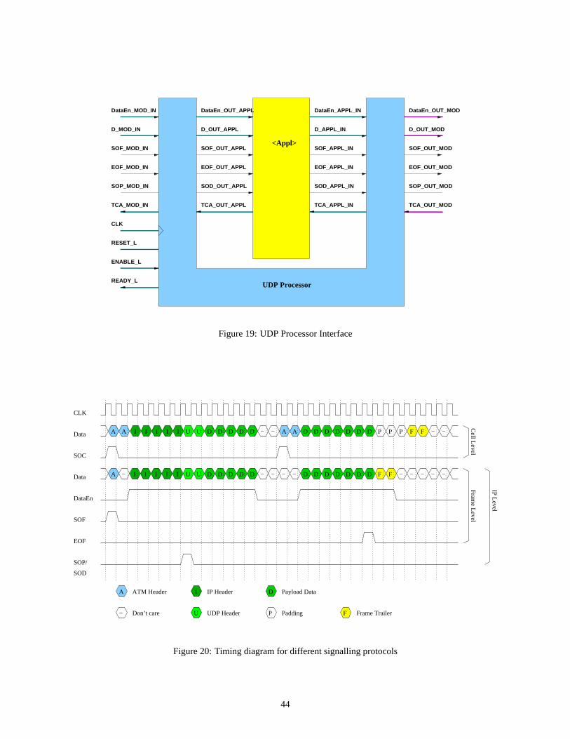
D_OUT_MOD
<Appl>
DataEn_MOD_IN
D_MOD_IN
SOF_MOD_IN
EOF_MOD_IN
CLK
RESET_L
ENABLE_L
READY_L
DataEn_OUT_MOD
SOF_OUT_MOD
EOF_OUT_MOD
DataEn_OUT_APPL
D_OUT_APPL
SOF_OUT_APPL
EOF_OUT_APPL
TCA_OUT_APPL
DataEn_APPL_IN
D_APPL_IN
SOF_APPL_IN
EOF_APPL_IN
TCA_APPL_IN
SOD_OUT_APPL SOD_APPL_IN
TCA_MOD_IN TCA_OUT_MOD
SOP_MOD_IN SOP_OUT_MOD
UDP Processor
Figure19: UDP ProcessorInterface
DataEn
SOF
EOF
Data
SOC
Data
SOD
SOP/
A A I I I I I U U D D D D D D D D D D D DA A− − P P P F F − −
A − I I I I I U D D D D D − − − − D D D D D D D F F − − − − −
A
−
I
U
U
FP
DATM Header IP Header
Don’t care Frame TrailerPadding
Payload Data
UDP Header
CLK
Cell Level
Fram
e Level
IP Level
Figure20: Timing diagramfor differentsignallingprotocols
44
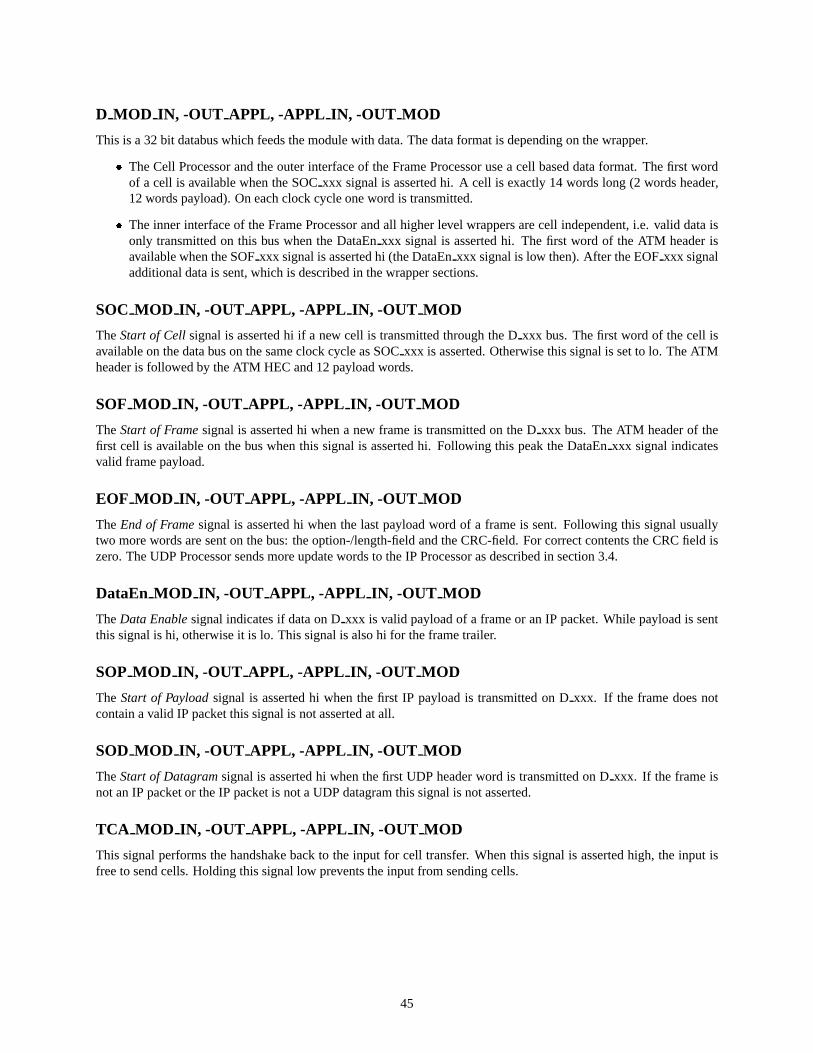
D MOD IN, -OUT APPL, -APPL IN, -OUT MOD
This is a 32 bit databuswhich feedsthemodulewith data.Thedataformatis dependingon thewrapper.
e TheCell Processorandtheouterinterfaceof theFrameProcessorusea cell baseddataformat. Thefirst wordof a cell is availablewhentheSOCxxx signalis assertedhi. A cell is exactly 14 wordslong (2 wordsheader,12wordspayload).Oneachclock cycleoneword is transmitted.
e Theinner interfaceof theFrameProcessorandall higherlevel wrappersarecell independent,i.e. valid dataisonly transmittedon this bus whenthe DataEnxxx signal is assertedhi. The first word of the ATM headerisavailablewhentheSOFxxx signalis assertedhi (theDataEnxxx signalis low then).After theEOF xxx signaladditionaldatais sent,which is describedin thewrappersections.
SOC MOD IN, -OUT APPL, -APPL IN, -OUT MOD
TheStart of Cell signalis assertedhi if a new cell is transmittedthroughtheD xxx bus. Thefirst word of thecell isavailableon thedatabuson thesameclock cycleasSOCxxx is asserted.Otherwisethis signalis setto lo. TheATMheaderis followedby theATM HEC and12 payloadwords.
SOF MOD IN, -OUT APPL, -APPL IN, -OUT MOD
TheStart of Frame signalis assertedhi whena new frameis transmittedon theD xxx bus. TheATM headerof thefirst cell is availableon thebuswhenthis signalis assertedhi. Following this peaktheDataEnxxx signalindicatesvalid framepayload.
EOF MOD IN, -OUT APPL, -APPL IN, -OUT MOD
TheEnd of Frame signalis assertedhi whenthe lastpayloadword of a frameis sent. Following this signalusuallytwo morewordsaresenton thebus: theoption-/length-fieldandtheCRC-field.For correctcontentstheCRCfield iszero.TheUDP Processorsendsmoreupdatewordsto theIP Processorasdescribedin section3.4.
DataEn MOD IN, -OUT APPL, -APPL IN, -OUT MOD
TheData Enable signalindicatesif dataon D xxx is valid payloadof a frameor anIP packet. While payloadis sentthis signalis hi, otherwiseit is lo. Thissignalis alsohi for theframetrailer.
SOP MOD IN, -OUT APPL, -APPL IN, -OUT MOD
The Start of Payload signal is assertedhi whenthe first IP payloadis transmittedon D xxx. If the framedoesnotcontaina valid IP packet thissignalis notassertedatall.
SOD MOD IN, -OUT APPL, -APPL IN, -OUT MOD
TheStart of Datagram signalis assertedhi whenthefirst UDP headerword is transmittedon D xxx. If the frameisnot anIP packetor theIP packet is nota UDP datagramthissignalis not asserted.
TCA MOD IN, -OUT APPL, -APPL IN, -OUT MOD
This signalperformsthehandshake backto the input for cell transfer. Whenthis signalis assertedhigh, the input isfreeto sendcells.Holding thissignallow preventstheinput from sendingcells.
45
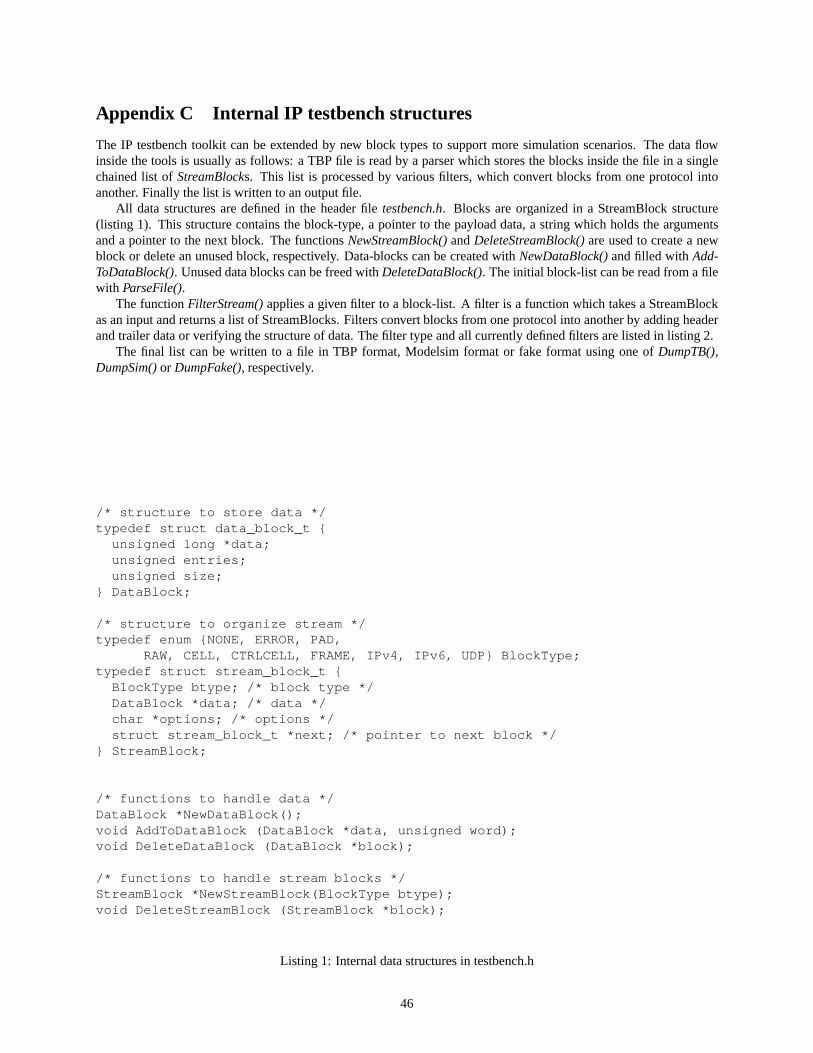
Appendix C Inter nal IP testbenchstructur es
The IP testbenchtoolkit canbe extendedby new block typesto supportmoresimulationscenarios.The dataflowinsidethetools is usuallyasfollows: a TBP file is readby a parserwhich storestheblocksinsidethefile in a singlechainedlist of StreamBlocks. This list is processedby variousfilters, which convert blocksfrom oneprotocol intoanother. Finally thelist is written to anoutputfile.
All datastructuresaredefinedin the headerfile testbench.h. Blocks areorganizedin a StreamBlockstructure(listing 1). This structurecontainsthe block-type,a pointerto the payloaddata,a stringwhich holdsthe argumentsanda pointerto thenext block. The functionsNewStreamBlock() andDeleteStreamBlock() areusedto createa newblock or deleteanunusedblock, respectively. Data-blockscanbecreatedwith NewDataBlock() andfilled with Add-ToDataBlock(). Unuseddatablockscanbefreedwith DeleteDataBlock(). Theinitial block-list canbereadfrom afilewith ParseFile().
ThefunctionFilterStream() appliesa givenfilter to a block-list. A filter is a functionwhich takesa StreamBlockasaninputandreturnsa list of StreamBlocks.Filtersconvertblocksfrom oneprotocolinto anotherby addingheaderandtrailerdataor verifying thestructureof data.Thefilter typeandall currentlydefinedfilters arelistedin listing 2.
The final list canbe written to a file in TBP format, Modelsimformat or fake format usingoneof DumpTB(),DumpSim() or DumpFake(), respectively.
/* structure to store data */typedef struct data_block_t {
unsigned long *data;unsigned entries;unsigned size;
} DataBlock;
/* structure to organize stream */typedef enum {NONE, ERROR, PAD,
RAW, CELL, CTRLCELL, FRAME, IPv4, IPv6, UDP} BlockType;typedef struct stream_block_t {
BlockType btype; /* block type */DataBlock *data; /* data */char *options; /* options */struct stream_block_t *next; /* pointer to next block */
} StreamBlock;
/* functions to handle data */DataBlock *NewDataBlock();void AddToDataBlock (DataBlock *data, unsigned word);void DeleteDataBlock (DataBlock *block);
/* functions to handle stream blocks */StreamBlock *NewStreamBlock(BlockType btype);void DeleteStreamBlock (StreamBlock *block);
Listing 1: Internaldatastructuresin testbench.h
46
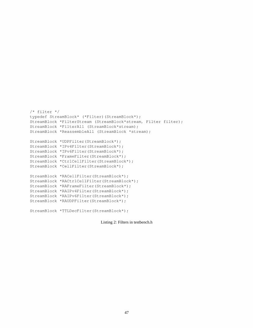
/* filter */typedef StreamBlock* (*Filter)(StreamBlock*);StreamBlock *FilterStream (StreamBlock*stream, Filter filter);StreamBlock *FilterAll (StreamBlock*stream);StreamBlock *ReassembleAll (StreamBlock *stream);
StreamBlock *UDPFilter(StreamBlock*);StreamBlock *IPv4Filter(StreamBlock*);StreamBlock *IPv6Filter(StreamBlock*);StreamBlock *FrameFilter(StreamBlock*);StreamBlock *CtrlCellFilter(StreamBlock*);StreamBlock *CellFilter(StreamBlock*);
StreamBlock *RACellFilter(StreamBlock*);StreamBlock *RACtrlCellFilter(StreamBlock*);StreamBlock *RAFrameFilter(StreamBlock*);StreamBlock *RAIPv4Filter(StreamBlock*);StreamBlock *RAIPv6Filter(StreamBlock*);StreamBlock *RAUDPFilter(StreamBlock*);
StreamBlock *TTLDecFilter(StreamBlock*);
Listing 2: Filtersin testbench.h
47
References
[1] Tom Chaney, J.Andrew Fingerhut,MargaretFlucke,andJonathanS. Turner. Designof a gigabitATM switch.TechnicalReportWU-CS-96-07,WashingtonUniversityin SaintLouis,1996.
[2] JohnW. Lockwood,JonS.Turner, andDavid E. Taylor. Fieldprogrammableportextender(FPX) for distributedrouting and queuing. In ACM International Symposium on Field Programmable Gate Arrays (FPGA’2000),pages137–144,Monterey, CA, USA, February2000.
[3] JohnW. Lockwood,Naji Naufel,JonS.Turner, andDavid E. Taylor. ReprogrammableNetwork PacketProcess-ing on theFieldProgrammablePortExtender(FPX). In ACM International Symposium on Field ProgrammableGate Arrays (FPGA’2001), pages87–93,Monterey, CA, USA, February2001.
[4] David E. Taylor, JohnW. Lockwood,andNaji Naufel. GeneralizedRAD ModuleInterfaceSpecificationof theField-programmablePorteXtender(FPX). Technicalreport,WUCS-01-15,WashingtonUniversity, Departmentof ComputerScience,July2001.
[5] David E. Taylor, JohnW. Lockwood,andNaji Naufel. RAD Module Infrastructureof theField-programmablePorteXtender(FPX).Technicalreport,WUCS-01-16,WashingtonUniversity, Departmentof ComputerScience,July2001.
[6] Toshiaki Miyazaki, Kazuhiro Shirakawa, MasaruKatayama,Takahiro Murooka, and Atsushi Takahara. Atransmutabletelecomsystem.In Proceedings of Field-Programmable Logic and Applications, pages366–375,Tallinn, Estonia,August1998.
[7] HamishFallsideandMichaelJ.S.Smith. InternetconnectedFPL. In Proceedings of Field-Programmable Logicand Applications, pages48–57,Villach, Austria,August2000.
[8] EmmanuelA. Arnould,FrancoisJ.Bitz, Eric C. Cooper, H. T. Kung,RobertD. Sansom,andPeterA. Steenkiste.Thedesignof Nectar:A network backplanefor heterogeneousmulticomputers.In Proceedings of the Third In-ternational conference on Architectural support for Programming Languages and Operating systems (ASPLOS-III), pages205–216,1989. Also availableasTechnicalReportCMU-CS-89-101,Schoolof ComputerScience,CarnegieMellon University, Pittsburgh.
[9] Wrapperwebpage.http://www.arl.wustl.edu/arl/projects/fpx/wrappers, July2001.
[10] ToddSproull,JohnW. Lockwood,andDavid E. Taylor. Controlandconfigurationsoftwarefor a reconfigurablenetworkinghardwareplatform. In submitted to Globecom 2001, SanAntonio,TX, USA, November2001.
[11] B-ISDN ATM adaptionallayerAAL FunctionalDescription.CCITT: RecommendationI.362,1991.
[12] B-ISDN ATM adaptionallayerAAL Specification.CCITT: RecommendationI.363,1991.
[13] PeterNewmanetal. Transmissionof flow labelledIPv4on ATM datalinks. InternetRFC1954,May 1996.
[14] FredBaker. Requirementsfor IP version4 routers.InternetRFC1812,June1995.
[15] IP testbench webpage. http://www.arl.wustl.edu/arl/projects/fpx/research/-iptestbench.html, July2001.
48