Embed Size (px)
Citation preview
Layered Nanocomposites For Neural Prosthetic Devices
by
Huanan Zhang
A dissertation submitted in partial fulfillment
of the requirement for the degree of
Doctor of Philosophy
(Chemical Engineering)
In The University of Michigan
2014
Doctoral Committee:
Professor Nicholas A. Kotov, Chair
Professor Cynthia A. Chestek
Professor Joerg Lahann
Professor Michael J. Solomon

Copyright Huanan Zhang 2014

Dedication
To my family, my mentors and my friends
ii
ACKNOWLEDGMENTS
This dissertation would not have been possible without the support and
contribution of many individuals. I would like to express my sincere gratitude to all
of them.
First, I would like to express my appreciation to Professor Nicholas A. Kotov
as my Ph.D advisor. He has been a tremendous mentor for me. He always supported
and encouraged me for my intellectual curiosity. He always gave me enlightened
feedback and suggestions when I faced challenges in my Ph.D study. His
perseverance, knowledge, creativity, intelligence, and kindness will always inspire
me in my future career.
I would also like to express my gratitude to my committee members,
Professor Joerg Lahann, Professor Michael J. Solomon, and Professor Cynthia A.
Chestek to discuss my research, offer me advice, and review my thesis.
I would like to thank the current and past member of the Kotov group for their
friendship and scientific discussions. Especially, Dr. Jian Zhu, Dr. Christine Andres,
Dr. Bongjun Yeom, Asish Misra and Terry Shyu have given me tremendous amount
of scientific feedback and technical assistance. I would also like to thank my
undergraduate students, Jimmy Shin, Betsy Gast, Samantha Rahmani for their
assistance with my experiments.
iii

I also deeply appreciate many collaborators I have worked with over the years.
I would like to thank Dr. Takashi D. Yoshida Kozai and Paras Patel for their
insightful advice and assistance. I would also like to thank Dr. Xueding Wang and Dr.
Scott Swanson for mentoring me on the neuroimaging project.
Lastly, I would like to thank my parents for their unconditional love and care.
I would also like to thank my friends for their companionship and support over the
years.
iv

TABLE OF CONTENTS
DEDICATION.............................................................................................................. ii
ACKNOWLEDGEMENTS......................................................................................... iii
LIST OF FIGURES ................................................................................................... viii
ABSTRACT................................................................................................................ xii
CHAPTER
1 Introduction ............................................................................................................. 1
1.1 Motivation ........................................................................................................... 1
1.2 Current Design of Neural Electrodes for Interfacing Central Nerve System...... 3
1.3 Brain Tissue Response to Chronically Implanted Electrodes ............................. 6
1.4 Material Components for Neural Prosthetic Devices........................................ 12
1.5 Layer-by-Layer (LbL) Assembled Nanocomposite and Its Applications in Neural Interface....................................................................................................... 19
1.6 Overview ........................................................................................................... 25
1.7 References ......................................................................................................... 27
2 Tissue Compliant Neural Implants from Microfabricated Carbon Nanotube Multilayer Composite ............................................................................................... 43
2.1 Abstract ............................................................................................................. 43
2.2 Introduction ....................................................................................................... 44
2.3 Materials and Methods ...................................................................................... 51
2.4 Results and Discussion...................................................................................... 56
2.5 Conclusions ....................................................................................................... 74
v
2.6 References ......................................................................................................... 75
3 Gold Nanoparticles for Neural Prosthetic Devices ............................................. 83
3.1 Abstract ............................................................................................................. 83
3.2 Introduction ....................................................................................................... 84
3.3 Materials and Methods ...................................................................................... 87
3.4 Results and Discussion...................................................................................... 92
3.5 Conclusion....................................................................................................... 105
3.6 References ....................................................................................................... 106
4 Aramid Nanofiber and Epoxy Composite as Multifunctional Insulation Material for Implantable Electronics.................................................................... 116
4.1 Abstract ........................................................................................................... 116
4.2 Introduction ..................................................................................................... 117
4.3 Materials and Methods .................................................................................... 121
4.4 Result and Discussion ..................................................................................... 125
4.5 Conclusion....................................................................................................... 140
4.6 References ....................................................................................................... 140
5 Flexible High Performance Nanocomposite Microelectrodes for Neural Interface ................................................................................................................... 146
4.1 Abstract ........................................................................................................... 146
4.2 Introduction ..................................................................................................... 147
4.3 Materials and Methods .................................................................................... 150
4.4 Result and Discussion ..................................................................................... 154
4.4 Conclusion....................................................................................................... 161
4.6 References ....................................................................................................... 161
6 Conclusion and Future Directions...................................................................... 168
6.1 Conclusion....................................................................................................... 168
vi

6.2 Future Directions............................................................................................. 171
vii
LIST OF FIGURES
Figure 1.1 Common types of NPD devices (A) Metal microarray electrodes16 (B) Planar silicon electrode39 (C) 3D silicon electrode array40
Figure 1.2 Tissue response to NPDs (A) Glial scar formation around the implanted silicon electrode20 (B) ultrasmall carbon fiber electrode to minimize tissue response52 (C) Magnitude of strain around implanted silicon electrode53 (D) Magnitude of strain around implanted polyimide electrodes53
Figure 1.3 Mode of electrode/tissue interface (A)Simplified schematic of the electrode/tissue interface (B) Circuit analog of the electrode/tissue interface
Figure 1.4 Advanced materials for neural interface (A) SEM image of sputtered IrO81 (B) SEM image of electrodeposited PEDOT70 (C) SEM image of LBL assembled CNT
Figure 1.5 LBL assembled Nanostrutures and its applications (A) Illustration of the LBL deposition process (B) AFM image of LBL assembled HgTe nanoparticles with PDDA100 (C) Neural stem cell differentiation on LBL assembled CNT film75 (D) Stability test of different advanced neural interface materials101
Figure 2.1 (A) Fabrication scheme of the nanocomposite electrodes combining LBL and MEMS-like microfabrication. (B) Optical image of composite electrodes on glass substrate.. (D) SEM image of a composite electrode with a width of 10 µm. The “window” in the parylene-C coating serves as the neural recording site and has high contrast with the insulating coating due to electrical conductivity of the LBL-made CNT composite. (E) The close-up SEM image of the CNT neural recording site on the 10 µm wide electrode.
Figure 2.2 (A) Cross-section SEM image of the fabricated electrodes (B) Cross-section SEM image of the recording site on the fabricated electrodes. Distortion of the parylene-C and composite layers of the device occurs due to sheer stress due to cutting. Note no delamination of CNT composite layer can be observed.
Figure 2.3 (A) Nanocomposite electrode on parylene-C sheet bent at 180 degrees to demonstrate flexibility (B) Tensile test of nanocomposite electrode, Young’s modulus of 2.2GPa.
Figure 2.4 (A) Typical impedance (Z) of the electrodes with different sizes of the functional sites. (B) Typical cyclic voltammetry of the electrodes with different sizes of the functional sites, sweep from 0.8 V to -0.6 V at 1V/s scan rate. (C) Cumulative
viii
electrochemical properties of the nanocomposite electrodes. Eight electrodes were tested for each size.
Figure 2.5 Schematic of the electrode/shuttle system
Figure 2.6 (A) Schematic of the photoacoustic microscopy (PAM) setup. (B) PAM image of two electrodes inserted into the brain. (C) MRI image of the implant in the y-z plane (Sagittal plane) (D) Zoom in MRI image of the y-z plane (Sagittal plane). (E) MRI image of the x-y plane (transverse plane). (F) Confocal microscopy of brain tissue and inserted electrode. Electrode was stained with FITC (green color) and cells were stained with toluidine blue (red color). (G) Cross-section SEM image of the electrode after brain insertion. There are three distinct layers as labeled in the graph.
Figure 2.7 (A) Harvested animal brain after recording experiment. (B) Low frequency signal recorded from the brain with the 10 µm wide nanocomposite electrode (100μm2 recording site) (C) Power spectrum of the low frequency signal recording, signal peak at 5 Hz. . Blank recording experiment in phosphate buffered saline (PBS) (D) Local field potential recorded from PBS. (E) Power Spectrum of the recorded local field potential.
Figure 3.1. (A) AFM image of 15 bilayers of Au NP LBL film. (B) AFM image of 25 bilayers of CNT LBL film. (C) First bilayer of Au NP LBL film. (D) Ellipsometric thickness of Au NP LBL films for different number of bilayers.
Figure 3.2 SEM images of Au NP film and CNT film. (A, B) SEM images of Au NP film at different magnifications. (C) Cross-section image of Au NP film. (D, E) SEM images of CNT film at different magnifications. (F) Cross-section image of CNT film.
Figure 3.3 (A) Fabrication process of the microelectrodes with LBL films of Au NPs and CNTs (1) deposition and development of the positive photoresist; (2) E-beam deposition of the metal gold; (3) lift-off of the metal gold layer; (4) deposition and development of the positive photoresist (5) deposition of the LBL film (6) lift-off of LBL film and deposition/development of insulating photo-resist layer. (B) Optical image of Au NP LBL film coated electrode. (C) Optical image of CNT LBL film coated electrode.
Figure 3.4 EDAX spectra of CNT (A, C) and Au NPs (B, D) LBL films before (A, B) and after (C, D) microfabrication on silicon substrates.
Figure 3.6 Circuit analog of the impedance data
ix
Figure 3.7(A) Sample confocal fluorescent image of LIVE/DEAD assay (Green:Live Red:Dead). (B) SEM image of Au NP/PDDA LBL film after insertion of rat brain.
Figure 4.1 Illustration of the spin coating process
Figure 4.2 (A) SEM image of ANF/Epoxy composite, six layers (B) SEM image of the cross section of ANF/Epoxy composite (C) SEM image of the cross section of layered ANF film (E) SEM image of the cross section of the dried ANF film with Epoxy
Figure 4.3 Metal adhesion test (A) Wet Cr etch of ANF/Epoxy composite, rectangular strip opening (B) Wet Cr etch of parylene, rectangular strip opening (C) Wet Cr etch of ANF/Epoxy composite, square opening (D) Wet Cr etch of parylene, square opening
Figure 4.4 (A) Illustration of the interfaces in IDE (B) Fabricated IDE structure (C) Zoom in IDE structure on parylene film (D) Zoom in IDE structure on ANF/Epoxy composite
Figure 4.5 (A) Lateral impedance of different IDEs (B) Transverse impedance of different IDEs
Figure 4.6 (A) NG108 cell culture on ANF/Epoxy composite (B) NG108 cell culture on parylene
Figure 4.7 Live/Dead Assay of NG108 cells on various substrates. (Green:Live Red: Dead) (A) NG108 cell culture on tissue culture coverslip glass (B) NG108 cell culture on parylene (C) NG108 cell culture on ANF/epoxy (D) NG108 cell culture on ANF/epoxy treated with 70% ethanol solution.
Figure 4.8 (A) Optical image of ANF/Epoxy composite and ANF/Epoxy/PEG composite (B) fluorescent image of ANF/Epoxy composite and ANF/Epoxy/PEG composite after albumin absorption
Figure 5.1 (A) Gold nanoparticle LbL nanocomposite deposited on the ANF/epoxy layer (B) Free standing flexible composite material with ANF/epoxy and gold nanoparticles (C) SEM image of the ANF/epoxy composite prior to LbL assembly (D) SEM image of the ANF/epoxy composite after LBL assembly
Figure 5.2 (A) Tensile test result of the all composite electrode materials (B) Magnitude of the impedance for a typical as fabricated electrodes
x
Figure 5.3 (A) Schematic of the fabrication proces (B) Photography of an all composite electrodes (C) The tip of the all composite electrodes before liftoff (D) The tip of the all composite electrodes after liftoff , while suspended in water
Figure 5.4 Visual cortex stimulus recording (A) Raw spike stream of on/off state, band pass filtered from 300 Hz to 5000 Hz (B) Peristimulus time histogram of the visual cortex during stimulus recording
xi
ABSTRACT
The motivation of this dissertation is developing neural prosthetic devices for chronic
brain-computer interface. To maintain a chronically sustainable brain-computer
interface, implantable devices should have minimal chronic inflammation,
mechanically compliance with neural tissue, and long term durability under
physiological conditions. Traditional neural prosthetic devices can seldom fulfill
these requirements. This dissertation presents a nanocomposite approach to design the
next generation neural prosthetic devices. The rationally designed nanocomposite can
achieve the combination of the desired material properties for neural prosthetic
devices, currently unattainable by traditional materials. In this dissertation, we first
fabricated a mechanically compliant neural electrode from carbon nanotubes. The
seamless integration of carbon nanotubes and polymer offered both mechanical
flexibility and electrical conductivity for neural prosthetic devices. Then we explored
other nanomaterials to design more exceptional nanocomposites. The gold
nanoparticle nanocomposite developed in this research outperformed carbon nanotube
composite in term of electrochemical performance. Additionally, we utilized the
nanocomposite approach to design flexible insulation material for implantable
electronic. By combining aramid nanofibers and epoxy resin, the composite material
has outstanding adhesion and biocompatibility. Lastly, we designed a
microfabrication process to combine gold nanoparticle composite and aramid
xii

xiii
nanofiber composite to create tissue compliant and high performance neural
electrodes.
1
Chapter 1
Introduction
1.1 Motivation
Neurological disorders and trauma injuries are among some of the most
challenging medical problems we face today. These conditions often have
devastating effects on patients and their familes. Neural prosthetic devices (NPDs) are
a class of medical devices that have the potential to revolutionize the diagnosis and
treatments of these neurological conditions. Generally, there are two classes of NPDs,
one interacts with the central nerve system and the other communicates with the
peripheral nerve system. Due to the large dissimilarity between the two biological
systems, the design parameters for each class of NPDs are distinctive from each
other.1 For peripheral system , cochlear implants2, 3 and pacemakers4, 5 are highly
developed and commercialized devices that utilized for restoring neural functionality
2
or regulating neural activity. For central nerve system, chronic deep brain
stimulation6 (DBS) demonstrated the ability to relieve symptoms of Parkinson’s7-9
and even Alzheimer’s disease.10 NPDs have also allowed patients of ayomyotrophic
lateral sclerosis to regain motor control.11 Recently, advances in brain-computer
interface have received increasing attention due to the possibility of using multi-site
recording NPD platforms for abstracting neural signals and controlling external
devices.12-15
Despite the initial clinical success, most of the NPDs for central nerve system
cannot retain a functional interface with neurons in the brain over a long period of
time.16-19 Chronic device failure is a complex problem related to inflammatory
response, low electrochemical performance, charge transport resistance at
tissue/electrode interface, and chemical stability of the electrode materials, etc.20, 21
To resolve these issues, it would require innovative design approach to tailor the
materials properties.
Nanomaterials offer possibilities to design the next generation NPDs22.
Nanomaterials have been utilized in many area of biomedical research, exemplified
by the tremendous amount of research on drug delivery23, 24 and tissue engineering24,
25. By combining nanomaterials with other traditional materials, we can create
nanocomposite with a combination of the desirable properties for NPDs to resolve
aforementioned issues in neural interface applications.
3
This dissertation will mainly discuss the issues and possible solutions for
NPDs interfacing with the cerebral cortex. First we will systematically evaluate the
current issues with NPDs, particularly materials challenges and investigate possible
nanocomposite materials to resolve these issues. We will also demonstrate that
nanocomposite materials from layer-by-layer (LBL) assembly can be fabricated into
functional devices.
Neural engineering is an interdisciplinary field, involves material science,
biomedical engineering, biology, and chemistry etc. In this introductory chapter, we
will first survey the development of current NPD designs, which include the
manufacturing technology, shapes, sizes, materials, and layouts of current NPDs.
Then we will examine more details related to the tissue responses of current NPD.
We then follow up by reviewing the different material components in the NPDs, the
methodologies to measure the material performance, and some current approaches in
material design to improve performance and mitigate tissue response. Lastly, we will
discuss on layer-by-layer (LbL) assembled nanocomposite as an excellent choice for
the next generation NPDs.
1.2 Current Design of Neural Electrodes for Interfacing the Central Nervous
System
Typically, there are two ways for NPDs to communicate with the nervous
system, and this is through electrical stimulation and recording.21 During electrical
4
stimulation, the neural electrode delivers charges to activate the targeted neurons,
thus facilitating electrical signal transduction of the damaged or defective neural
circuits. For example, muscle contraction can be stimulated externally by delivering
electrical charges to the related nervous system.26 Instead of electrical stimulation,
electrical recording is the detection of the neural signal in the nervous system. In this
system, the neural electrode serves as a passive device that extracts information from
the neural system to the external devices. Neural recording technology has been the
essential development for brain-computer interface, where electrodes can extract
electrical signals from the brain to the external electronics, and the information can be
decoded and understood for the control of external devices.27
Metal wires have been traditionally used as electrodes for fundamental and
clinical neuroscience due to their excellent electrical conductivity. By using metal
wires, Hodgkin and Huxley conducted experiments on a single neuronal fiber to
understand signal transduction in neurons, which became the foundation of modern
neuroscience.28 The next revolution in neural electrode technology came from the
advances in micromachining. Advanced micromachining technology allows for the
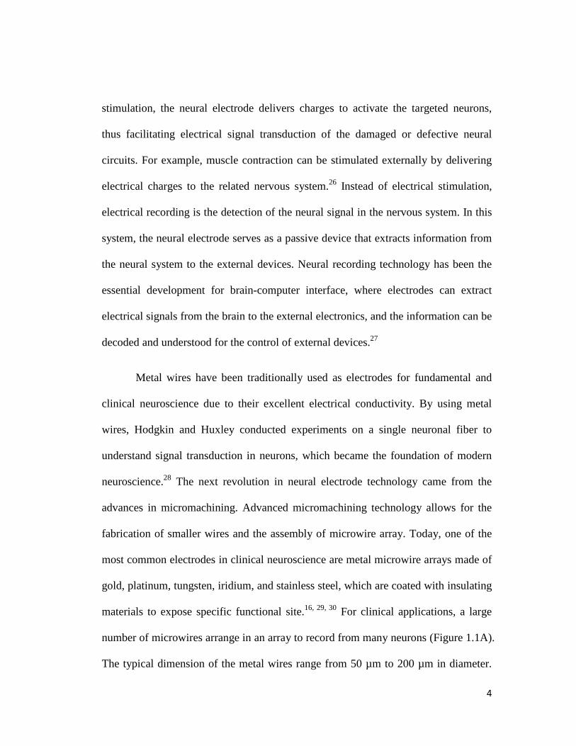
fabrication of smaller wires and the assembly of microwire array. Today, one of the
most common electrodes in clinical neuroscience are metal microwire arrays made of
gold, platinum, tungsten, iridium, and stainless steel, which are coated with insulating
materials to expose specific functional site.16, 29, 30 For clinical applications, a large
number of microwires arrange in an array to record from many neurons (Figure 1.1A).
The typical dimension of the metal wires range from 50 µm to 200 µm in diameter.
5
These multielectrode arrays allow the researchers to acquire single neural signals
from a large area of the motor cortex for precise prosthetic control, and eventually led
to the demonstration of close-looped brain-computer interface in monkeys.31
The next revolution in NPDs also originated from another advanced
manufacturing technique. Silicon based microfabrication technology has been the
main driving force for advanced neural electrode design for the past 30 years.32-34 It
offers us unprecedented control over the size, shape, and spacing of the neural
electrodes and functional sites35. In addition, one could also integrate other electronic
components, such as signal processing units36, 37 and wireless transmitting units38 with
the neural electrode to achieve other functionalities. The advancement in silicon
microfabrication technology allows increasingly smaller electrodes and higher density
electrode arrays, which further leads to better spatial resolution and signal-to-noise
ratio. The electrode design includes planar configuration and 3D configuration.
(Figure 1.1B and 1.1C). The original planar array was fabricated from a single thin
sheet of silicon that is 100um wide and 15um thick with several recording sites along
the shank.35 The silicon 3D array was first developed at the University of Utah.34 A
block of silicon was etched,doped and heat-treated to create an array of microneedle-
like structures, which is very similar to the microwire arrays.
6
Figure 1.1 Common types of NPD devices (A) Metal microarray electrodes16 (B) Planar silicon electrode39 (C) 3D silicon electrode array40
1.3 Brain Tissue Response to Chronically Implanted Electrodes
1.3.1 The Invasive Nature of NPDs and Cellular Responses from Brain Tissue
Although significant progress has been made in the past several decades in
terms of electrode design, the current devices are uable to retain their functionalities
over a long period. The longest functional recording device sustained its functionality
in vivo over a year.41 This is still much farther from the targeted lifetime for chronic
neural implants, which should retain their functionality over decades. Many studies
suggest that one of the main causes for decreasing recording ability is the
inflammatory response of the brain tissue toward implanted devices.20 In order to
design better chronic neural implants, we should first understand the cells responsible
for the inflammatory response and the key elements that trigger inflammatory
responses. This would allow us to design better electrodes to mitigate these issues.
7
Although the main functional cell type for communication in the brain is the
neuron, it constitutes less than 25% of the total cells in the brain. Other majorities of
the brain cells include glial cells (oligodendrocytes, astrocytes, and microglia) and
vascular cells. Astrocytes and microglia are the cells responsible for inflammatory
response and other regulatory functions of the brain.42 Upon activation of astrocytes
and microglia, both cells produce neural toxins and highly reactive chemical species,
as a part of defense mechanism in the brain.42
From previous simulation and experiment studies, we can conclude that the
electrodes need to be in close proximity to the targeted neuron for single unit
recording (between 50 um to 100um).43, 44 Therefore, all electrodes for single unit
recording are invasive and inevitably create trauma injuries during initial insertion to
the brain. Studies related to initial trauma injuries have shown that indeed, initial
trauma injuries activate both astrocytes and microglia.45, 46 However, as soon as six
days after initial injury, the study observed a significant reduction of excess fluids and
damages to cellular components.47 After several week and months, the initial trauma
wound will heal and no tracks of the initial electrode insertion can be observed.48, 49
This indicates that the chronic existence of the electrodes contribute to the long-term
inflammatory response, not the initial trauma injuries.
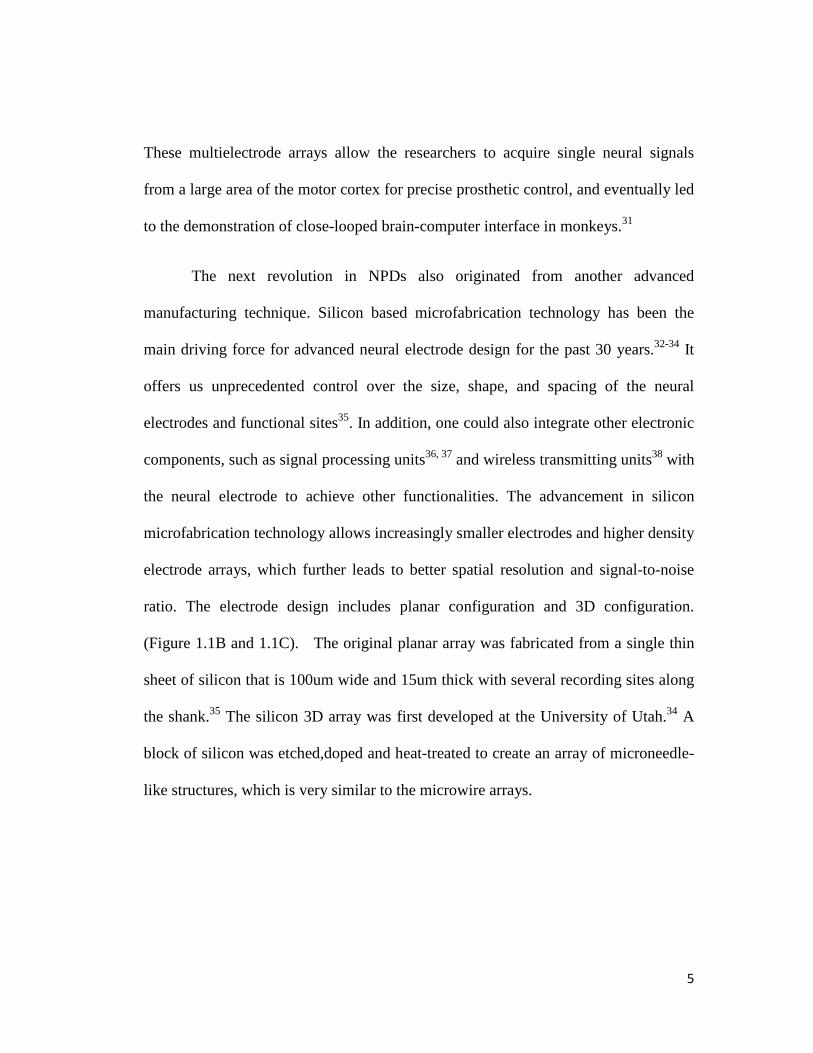
Long-term inflammatory responses in the brain around electrodes is
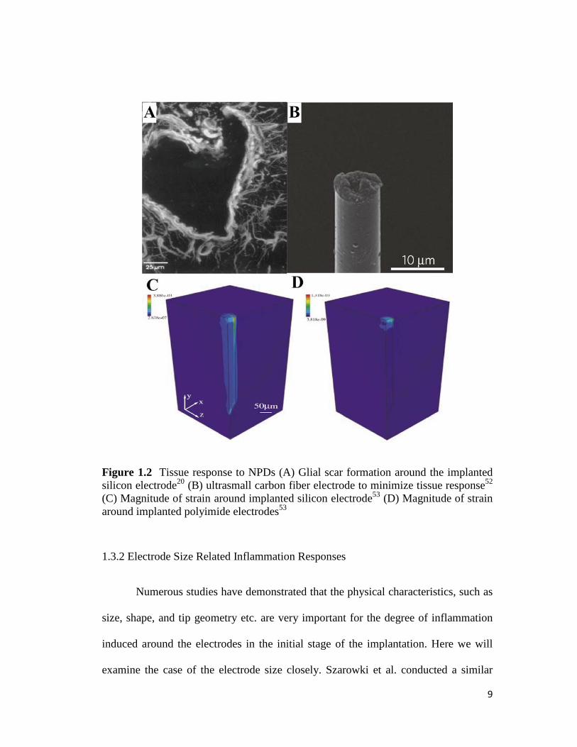
exemplified by glial scar formations around the electrode after weeks of the
implantation (Figure 1.2A).50 The process is very similar to foreign body
8
encapsulation in other parts of the body. Evidently, the glial scar creates an insulating
barrier between the electrodes and neurons, and prevents the successful recording of
the neurons. An immune staining study revealed that the main component of the glial
scar is reactive astrocytes, which further suggests that glial scar formation is closely
related to inflammatory responses.46, 51 time course studies also suggested that the
reactive astrocyte extended several hundred of microns away from the electrodes.46, 50
The exact mechanism and purpose of the glial scar are uncertain in the scientific
community. However, for the last decade, much research has been devoted to
designing optimal electrodes for minimizing the glial scar formation. Empirical
studies have unveiled several possible routes of electrode design to reduce
inflammation.
9
Figure 1.2 Tissue response to NPDs (A) Glial scar formation around the implanted silicon electrode20 (B) ultrasmall carbon fiber electrode to minimize tissue response52 (C) Magnitude of strain around implanted silicon electrode53 (D) Magnitude of strain around implanted polyimide electrodes53
1.3.2 Electrode Size Related Inflammation Responses
Numerous studies have demonstrated that the physical characteristics, such as
size, shape, and tip geometry etc. are very important for the degree of inflammation
induced around the electrodes in the initial stage of the implantation. Here we will
examine the case of the electrode size closely. Szarowki et al. conducted a similar
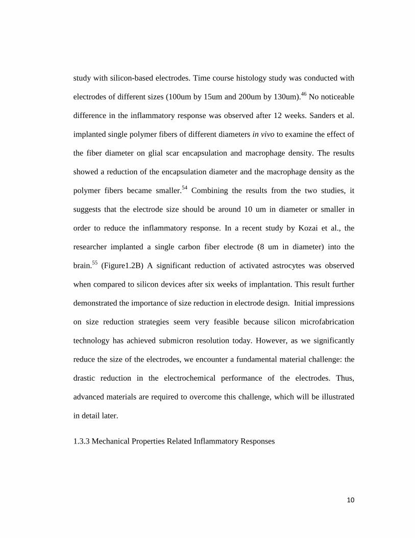
10
study with silicon-based electrodes. Time course histology study was conducted with
electrodes of different sizes (100um by 15um and 200um by 130um).46 No noticeable
difference in the inflammatory response was observed after 12 weeks. Sanders et al.
implanted single polymer fibers of different diameters in vivo to examine the effect of
the fiber diameter on glial scar encapsulation and macrophage density. The results
showed a reduction of the encapsulation diameter and the macrophage density as the
polymer fibers became smaller.54 Combining the results from the two studies, it
suggests that the electrode size should be around 10 um in diameter or smaller in
order to reduce the inflammatory response. In a recent study by Kozai et al., the
researcher implanted a single carbon fiber electrode (8 um in diameter) into the
brain.55 (Figure1.2B) A significant reduction of activated astrocytes was observed
when compared to silicon devices after six weeks of implantation. This result further
demonstrated the importance of size reduction in electrode design. Initial impressions
on size reduction strategies seem very feasible because silicon microfabrication
technology has achieved submicron resolution today. However, as we significantly
reduce the size of the electrodes, we encounter a fundamental material challenge: the
drastic reduction in the electrochemical performance of the electrodes. Thus,
advanced materials are required to overcome this challenge, which will be illustrated
in detail later.
1.3.3 Mechanical Properties Related Inflammatory Responses
11
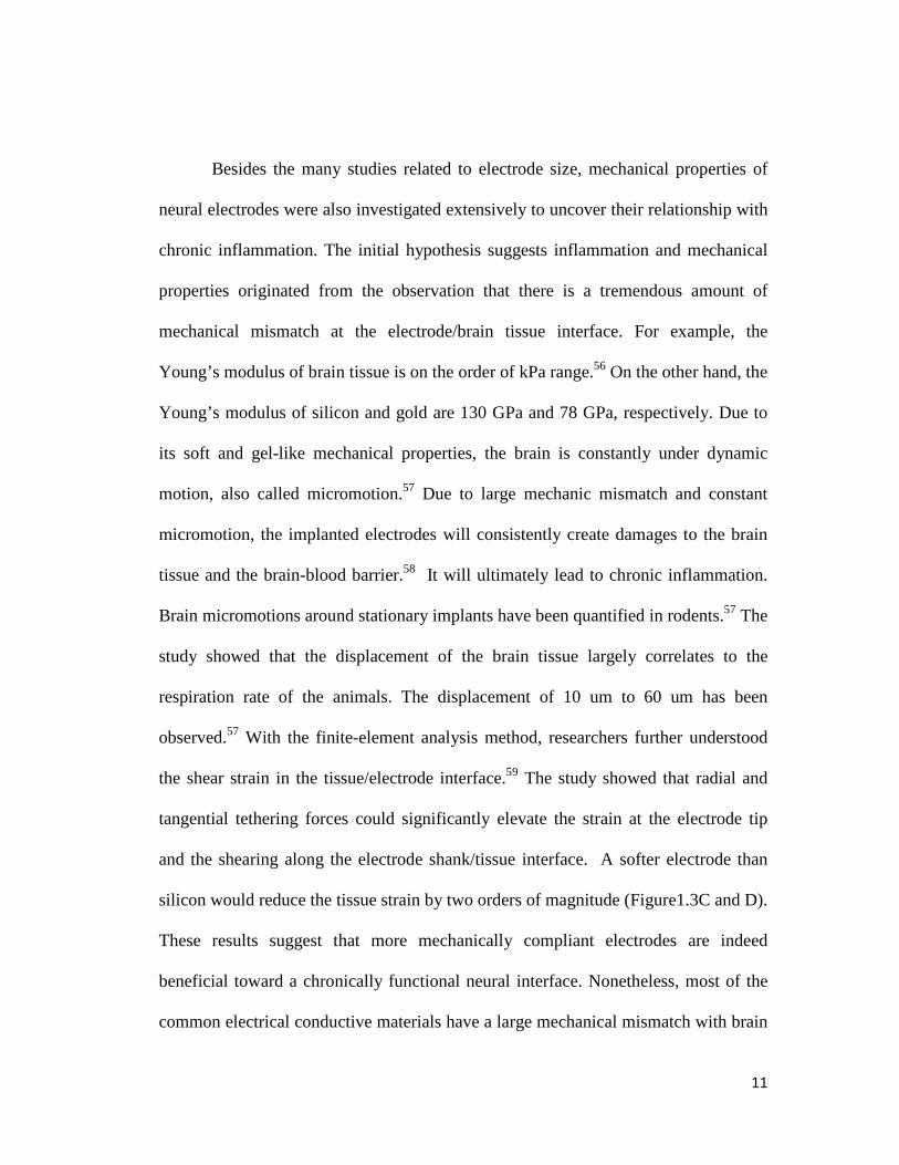
Besides the many studies related to electrode size, mechanical properties of
neural electrodes were also investigated extensively to uncover their relationship with
chronic inflammation. The initial hypothesis suggests inflammation and mechanical
properties originated from the observation that there is a tremendous amount of
mechanical mismatch at the electrode/brain tissue interface. For example, the
Young’s modulus of brain tissue is on the order of kPa range.56 On the other hand, the
Young’s modulus of silicon and gold are 130 GPa and 78 GPa, respectively. Due to
its soft and gel-like mechanical properties, the brain is constantly under dynamic
motion, also called micromotion.57 Due to large mechanic mismatch and constant
micromotion, the implanted electrodes will consistently create damages to the brain
tissue and the brain-blood barrier.58 It will ultimately lead to chronic inflammation.
Brain micromotions around stationary implants have been quantified in rodents.57 The
study showed that the displacement of the brain tissue largely correlates to the
respiration rate of the animals. The displacement of 10 um to 60 um has been
observed.57 With the finite-element analysis method, researchers further understood
the shear strain in the tissue/electrode interface.59 The study showed that radial and
tangential tethering forces could significantly elevate the strain at the electrode tip
and the shearing along the electrode shank/tissue interface. A softer electrode than
silicon would reduce the tissue strain by two orders of magnitude (Figure1.3C and D).
These results suggest that more mechanically compliant electrodes are indeed
beneficial toward a chronically functional neural interface. Nonetheless, most of the
common electrical conductive materials have a large mechanical mismatch with brain
12
tissue. This imposes another material challenge to NPD design: engineering of
flexible and soft electrical conductors.
1.4 Material Components for Neural Prosthetic Devices
Based on the previous studies on the tissue response of the chronic implants,
we can conclude that the next generation of neural prosthetic devices requires a
complete redesign of the material components. All neural electrodes primarily consist
of two major material components: electrical components and insulation components.
Both components are equally important in terms of electrode engineering as both
components contribute to the mechanical properties of the electrode, the size of the
electrodes, and the functionality of the electrodes. Electrical components are
electrically conductive materials of the electrodes that sense the flux of the ions
during neuron activation; and sequentially transduce the signal to the processing unit.
The insulation components are typically dielectric materials that protect the electrical
components of the electrodes and define the specific recording site of the electrodes.
They are the materials have the most contact with the brain tissue.
1.4.1 Electrical Components of Neural Prosthetic Devices
As mentioned previously, electronically conductive materials like metal and
doped silicon have been used as the electrical components of the electrodes for
obvious reasons: electrical conductors are exceptional for transducing the electrical
13
field change to the signal-processing unit in solid-state electronics. An electrical
conductor is an excellent choice if the main conduction mechanism is based on
electrons. However, neural tissues mostly consist of fluids with ions instead of
electrons. Ions are also the main signal transduction carrier for neurons. The
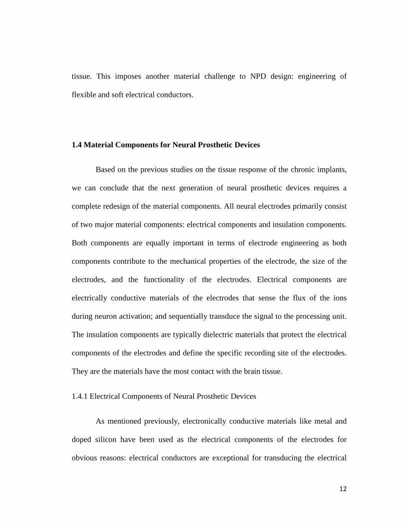
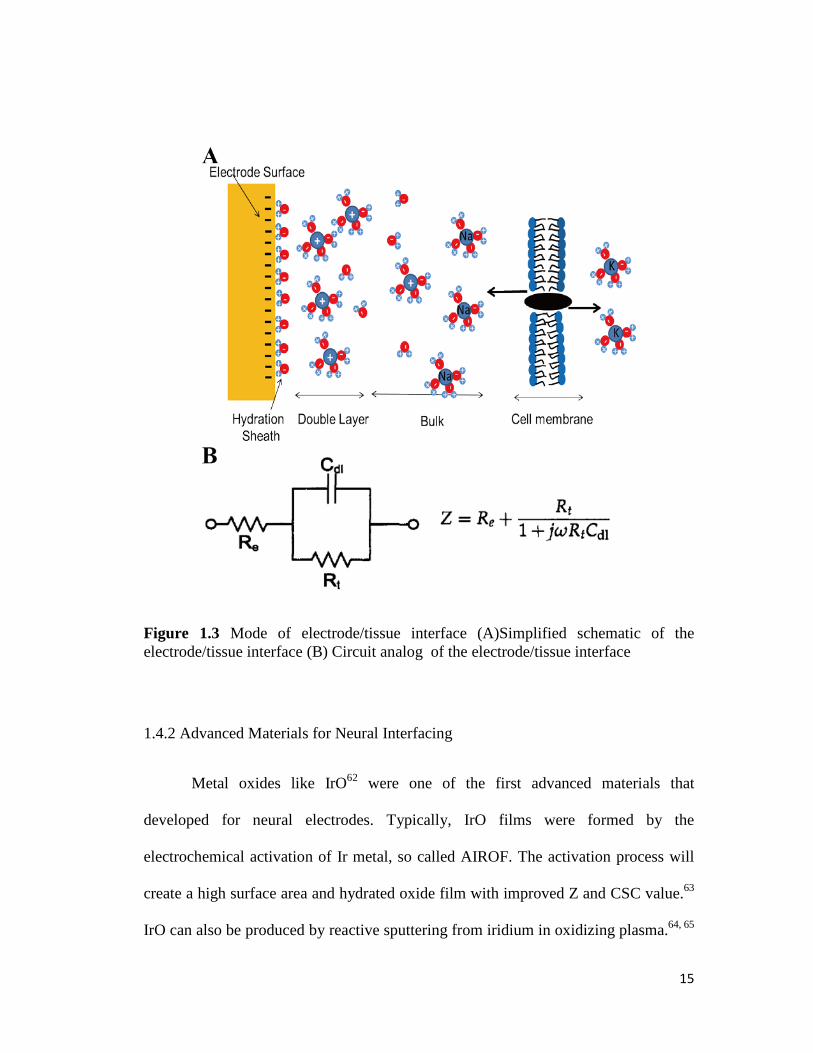
electrodes operate at the interface between the ion transport to the electron transport,
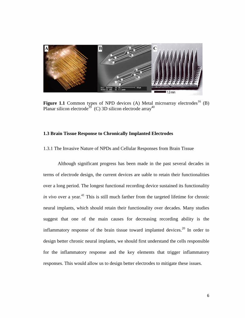
where the majority of the resistance comes from (Figure 13A).21 Therefore, an
excellent neural electrode is defined by its low resistance at the electrode/tissue
interface, not the electrical conductivity.60 The main parameter to characterize the
resistance at the electrode/tissue interface is electrochemical impedance (Z).
Electrochemical impedance is typically measured by electrochemical impedance
spectroscopy. The measurement is conducted over a large frequency range (1 Hz to
10^5 Hz) with a very small amount of current. With the voltage response data, one
can reconstruct a circuit model with basic electrical components, such as resistors and
capacitors. It is a valuable tool to investigate the interfacial properties. In the
electrode/tissue case, we can model the interface as a resistor and a capacitor in
parallel with each other (Figure 1.3B). 61 The magnitude of the impedance in this case
represents the overall resistance at the interface and the amount of charge stored at the
interface. Impedance data is arguably the most important parameter to estimate the
recording ability of the electrodes. A high impedance value normally correlates a
decrease in electrode functionality; given no other malfunction occurs at the same
time.21
14
Cyclic voltammetry (CV) is another common technique used to characterize
electrodes. CV experiments typically scan a voltage window at a specific scan rate.
The instrument will record voltage vs. current. From the CV scan, charge storage
capacity (CSC) can be calculated. CSC indicates the interfacial capacitance at the
electrode/tissue interface, which is also a component in the impedance measurement.
In addition, the interfacial chemical reactions can also be probed by the CV
experiments, which offer information on the chemical stability of the interface.26
Studies have shown that the Z and CSC of the metals diminish significantly as
the size of the electrode reduces. Therefore, there is a major challenge to reducing
electrode size while retaining electrode functionality. The Z and CSC value have a
close relationship with the conductivity and the surface area of the electrodes. The
perfect smooth surface of the metals could have contributed to the reduction of the Z
and CSC value. Therefore, many materials have been developed to enhance the Z
and CSC values, include Iridium oxide (IrO), conducting polymers, and carbon
nanotubes (CNTs) etc.
15
Figure 1.3 Mode of electrode/tissue interface (A)Simplified schematic of the electrode/tissue interface (B) Circuit analog of the electrode/tissue interface
1.4.2 Advanced Materials for Neural Interfacing
Metal oxides like IrO62 were one of the first advanced materials that
developed for neural electrodes. Typically, IrO films were formed by the
electrochemical activation of Ir metal, so called AIROF. The activation process will
create a high surface area and hydrated oxide film with improved Z and CSC value.63
IrO can also be produced by reactive sputtering from iridium in oxidizing plasma.64, 65
16
However, delamination of IrO on metals have been observed in some studies. This
will induce reduction of the CSC and Z over time and affect the efficiency of the
devices.63, 66, 67
The common conducting polymers for NPDs are polypyrrole and
polythiophene. Poly(3,4 ‐ ethylenedixoythiophene) (PEDOT), which is a
polythiophene based polymer, has attracted a lot of attention due to its
biocompatibility and chemical stability.68-70 There are several advantages of using
conductive polymers in NPDs, including biocompatibility, limited toxic effects, and
easy functionalization. Through electrochemical deposition, polymers can be
localized in a specific site with controlled thickness. Conductive polymers may also
act as delivery agents for biologically active molecules and drugs that could be
released in response to electrical stimulation.71-73
Carbon nanotubes (CNTs) are another emerging material that have been
investigated extensively over the past decade for neural interface applications.74-79
Metallic CNTs are highly conductive and with a current density of two or three
magnitudes higher than metals, like aluminum and copper.80 Their high conductivity
and unique 1D structure offer opportunities to engineer high performance neural
interface devices. The biocompatibility of the CNT has been evaluated with different
types of cell liness. Patterned CNTs can support neural adhesion and growth. Study
has demonstrated that the CNT coating can improve the recording quality in

17
primates.79 CNT based layer-by-layer composites have also been investigated for
neural interface applications. They will be discussed in greater detail later.
Although great efforts have been invested in developing materials with
improved Z and CSC, all of the aforementioned materials have been utilized as a
coating for the tradition style of the electrodes. They can improve the electrochemical
parameters of the smaller silicon or metal electrode. Nevertheless, they do not resolve
the issue of mechanical mismatch. In order to resolve both issues (size and
mechanical properties) simultaneously, other material design strategies are required to
develop both flexible, electrically conductive, and high electrochemical performance
materials. This issue will be addressed specifically in this dissertation.
Figure 1.4 Advanced materials for neural interface (A) SEM image of sputtered IrO81 (B) SEM image of electrodeposited PEDOT70 (C) SEM image of LBL assembled CNT
1.4.3 Insulation Components for Neural Prosthetic Devices
18
Although insulation components of the NPDs do not participate in signal
transduction, they still play a key role in device functionality. First, insulation
components protect the electrical wires of the electrodes from corrosion and
degradation of environmental chemicals. Second, insulation components also isolate
individual electrodes in the array configuration to prevent short circuit and cross talk
between electrodes. Third, insulating components define the specific recording sites
of the electrode. The size of the recording site determines the quality and the
specificity of neural recordings. All of these functionalities largely depend on the
strong adhesion between the insulation components and the electrical components of
the electrodes.82, 83 Delamination of the insulating components will result in device
failure. In silicon-based devices, silicon oxide and silicon nitride are commonly used
as an insulating layer. However, the mechanical properties of the silicon oxide and
silicon nitride also have a large mismatch with the brain tissue. Therefore, many
polymeric materials were considered as an insulating layer. Teflon, polyester, epoxy
basin, polyimide, and parylene have all been utilized in electrode fabrication.20 Many
flexible electrodes have been developed by combining polymer-based insulation
materials with metals in order to reduce the mechanical mismatch at the
electrode/tissue interface.84-87 This strategy further improves the mechanical
mismatch. However, it still relies on metals as the electrical components, which still
has a large mechanical mismatch with brain tissue. Furthermore, many polymeric
insulating layers have adhesion and delamination issues, due to the large surface
energy difference between the insulation layer and the electrical layer. This
19
significantly hinders the long term functionality of the devices.82 For instance,
parylene is an emerging material as insulating layer for neural electrodes. It is FDA
approved, chemically inert, and has low oxygen/water permeability. Nevertheless, the
hydrophobic nature of the material leads to poor adhesion on metals and affect the
device performance.82
The insulating components protect the electrical components of the electrode.
Therefore, it has the most interaction with the surrounding brain tissue. Its surface
properties and mechanical properties have directly effect on how the surrounding
brain tissue reacts to the neural electrode. Nonetheless, this close interaction also
offers opportunities to engineering the surface morphology and bioactivity of the
insulating component, which could possibly lead to improved inflammatory responses.
Using bioconjugation techniques, anti-inflammatory coating can be attached to
electrode surfaces. Dexamethasone, an anti-inflammatory coating on neural
electrodes showed a reduction in microglia and macrophages around the electrodes.88,
89 Other anti-inflammatory drug coatings and neural adhesion coatings also resulted
in a decreasing amount of activated astrocytes.90-96 Together, these demonstrated the
importance of modulating the surface bioactivity of insulating layers.
1.5 Layer-by-Layer (LbL) Assembled Nanocomposite and its Applications in
Neural Interface
1.5.1 Fundamentals of LbL Assembly
20
Layer-by-layer (LbL) assembled thin film composites are tightly alternating
monolayers of oppositely charged materials. The assembly is based on the principle
of charge-interaction, which was originally introduced for polyelectrolytes by Decher
et al. in 199297 independently of the earlier version of the same technique introduced
by Iler.98 All material surfaces have a net charge once immersed in the solution due to
oxidation, hydrolysis, and preferential adsorption of ions.99 When a negatively
charged surface is immersed in a solution of positive polyelectrolyte, such as
poly(dimethyldiallylammonium chloride) (PDDA), the positive electrolyte absorbs
onto the surface. After rinsing with water to remove all of the loosely bound
polyelectrolytes, the net charge on the surface would be positively charged from the
remaining monolayer of polyelectrolyte. This surface could then be immersed in a
solution with a negative polyelectrolyte and the net charge on the surface would
reverse to negative. With a cyclic process, a multilayer film of alternating
polyelectrolyte monolayers can be deposited on the surface with controlled structure
and thickness. This process is not limited to polyelectrolytes. Many nanomaterials are
dispersed in a solution with a net charge and could be used as a component in the LbL
assembly process creating textures and nanostructures based on the nanomaterial.
(Figure 1.5A) However, because of the multilayer nature of the LbL process, it allows
a homogenous high loading of nanoscale components in the material matrix. With
simple instruments, LbL assembly can also easily control coating thickness with
nanoscale accuracy, incorporating different material components, and adjusting other
relevant properties to achieve multiple functionalities. It is especially relevant for
21
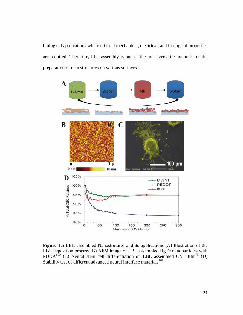
biological applications where tailored mechanical, electrical, and biological properties
are required. Therefore, LbL assembly is one of the most versatile methods for the
preparation of nanostructures on various surfaces.
Figure 1.5 LBL assembled Nanostrutures and its applications (A) Illustration of the LBL deposition process (B) AFM image of LBL assembled HgTe nanoparticles with PDDA100 (C) Neural stem cell differentiation on LBL assembled CNT film75 (D) Stability test of different advanced neural interface materials101
22
1.5.2 The LbL Assembled Nanostructure for Neural Interface Applications
LbL-assembled nanostructures have many electrochemical advantages for
neural stimulation by significantly increasing the electrochemical surface area of the
stimulating electrode, thus enhancing the charge-transport capability.21 Since LbL
assembly is a bottom up fabrication method, it can be applied to a variety of electrode
surfaces. The versatility of the LbL system offers opportunities to fabricate
nanostructures with various nanocomposites of the most diverse composition and
nanoscale organization incorporating metal nanoparticles (NPs), semiconductor NPs
also known as quantum dots (QDs), and carbon nanotubes (CNTs). Selecting
nanomaterials based on unique electrical and optical properties allow for flexibility in
different modes of neural stimulation (direct current or photostimulation). Free
standing film from LbL assembly cannot only retain excellent electrochemical
properties, but also offers mechanical flexibility and high mechnical strength.102 As
mentioned previously, flexible neural electrodes are believed to play an important
role in improving chronic in vivo tissue integration and reducing chronic
inflammation. Recent work indicates that LbL-assembled film can be successfully
patterned with lithography techniques opening new opportunities for designing neural
electrodes103
Semiconductor nanoparticles or quantum dots (QDs) are a unique class of
nanomaterials that are both optically and electrically active. Thus, photocurrents can
be generated and utilized for neural stimulation by QDs. Moreover, due to the
23
quantum confinement effect, QDs can be tailored to respond to specific wavelengths
of light when compared with bulk semiconductor materials. By combining both the
photoelectric and quantum confinement effect, nanostructures can be engineered to
stimulate neurons with specific spectral and electrical responses. By applying LbL
assembly of mercury telluride (HgTe) nanoparticles and PDDA, polyelectrolyte-
nanostructured films have been created with photostimulation capabilities.104 The
nanoscale features can be clearly observed under an atomic force microscopy (Figure
5.1B). Neuroblastoma/glioma hybrid cells (NG108) were successfully cultured and
differentiated on the HgTe/PDDA film. While stimulating with a 532 nm laser,
depolarization of the differentiated cells on HgTe/PDDA surface was observed, as
measured with a standard patch-clamp setup.
CNTs have electrical properties, chemical stability and desirable dimensions
to create nanostructures suitable for neural modulation. They have drawn much
attention for neural interface applications over the past decade. LbL-assembled CNT
nanostructures combine excellent electrical conductivity, biocompatibility, and
strength to advance neural interface applications. A single-walled carbon nanotube
(SWNT)/polyelectrolyte LbL film successfully supported and stimulated
neuroblastoma/glioma hybrid cells (NG108)75, 105. In a systemic comparison study,
LbL-assembled CNTs showed lower impedance and higher CSC compared to
electrochemically deposited PEDOT and iridium oxide.101 After 300 fast charging
cycles, the CNT film retained 95% of its CSC without any surface cracks compared
to PEDOT and iridium oxide, which showed minor or major cracks, respectively
24
(Figure 1.6D). The structural stability of the LbL CNT nanostructures is related to the
homogenous high loading of CNT in the polymer matrix and the close interaction
between each nanoscale layer. The homogenous loading of CNT in the polymer
matrix enables the development of materials that are mechanically strong and flexible.
Flexibility of the implantable neural electrode is believed to be a critical parameter
for in vivo implantation, and prevents glial encapsulation of the nanostructure
electrode site.
LbL-assembled nanostructures have demonstrated superior electrochemical
performance over other materials. Nevertheless, next generation devices for neural
stimulation require not only outstanding electrical performance, but also the ability to
facilitate and promote cell growth. One of the advantages of LbL-assembled
nanostructures is their ability to control composition and surface properties to
promote cell growth and enhance biocompatibility, while maintaining electrical
performance.
To illustrate the biocompatibility of the LbL-assembled nanostructure,
previous work indicates that LbL-assembled SWNT nanostructures support the
growth and differentiation of neural stem cells.75 Unlike common model cell lines,
neural stem cells are very sensitive to their culture environment and other physical
and chemical signals. Here, the SWNT nanostructures did not alter the progression of
neural stem cell differentiation. To demonstrate the versatility of the LbL method
further, an extracellular matrix protein (laminin) was incorporated as a
25
complementary layer into the LbL film with SWNTs to create biocompatible
nanostructures. By creating a laminin/SWNT composite, cell adhesion was enhanced
through the adhesion-promoting nature of laminin and the nanoscale features of the
SWNTs (Figure 1.6C).106 This example demonstrated the successful differentiation of
neural stem cells and the ability to stimulate the neural cells. It also illustrates how
LbL-assembled nanostructures could be an excellent tool for the multifunctional
engineering of nanostructures.
Other than improving cell adhesion and biocompatibility, one can further
incorporate other functional components into the LbL-assembled nanostructures.
With this approach, it is possible to prepare biologically active neural modulation
devices.107 To demonstrate this concept, a plasmid DNA layer was deposited on top
of an electrically active LbL CNT nanostructure. The plasmid DNA on the CNT
nanostructure transfected neural cells with greater efficiency compared to traditional
solution-based methods.
1.6 Overview
Through close examination of the current NPD technology and tissue
responses to the current NPDs, we can conclude that material innovation is necessary
in order to develop the next generation of NPDs. There are several requirements for
the new materials to be utilized in NPDs. In terms of the electrical component: (1)
excellent electronic conductors for electrical signal transduction to the signal
26
processing unit (2) exceptional electrochemical performance for enhancing the ability
to interface with ions in the physiological condition and minimizing the footprint of
the devices and, (3) the mechanic properties should match with the brain tissue as
close as possible to minimize any damages from mechanic strain. In terms of the
insulation component: (1) superb adhesion properties to the electrical component of
the NPD (2) chemically and biologically inert (3) low oxygen and water permeability
and, (4) has the ability to be functionalized at the surface to modulate biological
activities.
Nevertheless, it is very difficult for traditional materials to acquire all of the
necessary requirements for neural interface applications. LbL assembled
nanocomposites offer unique opportunities to revolutionize the field of NPDs. LbL
assembled nanocomposites have demonstrated both mechanically flexible and
excellent electrical conductivity in previous studies. Furthermore, the LbL assembly
method offers us the ability to fine-tune the material properties for specific
applications. We can modulate among mechanical properties, electrical properties,
electrochemical performance, biocompatibility, etc.
This dissertation is focused on the design and fabrication of LbL
nanocomposites for fully functional NPDs. Chapter 2 further examines the
mechanical compliance of the electrodes with brain tissue and establishes the formal
concept of tissue compliant neural electrodes. Then it demonstrates the tissue
compliance of the LbL assembled CNT composite and its ability to be integrated into
27
fully functional devices in vivo . Chapter 3 looks beyond CNT as a fundamental
nanomaterial for neural interface. It explores the ability of other nanomaterials to
create nanocomposites with superior electrical and electrochemical properties to that
of CNT. Chapter 4 examines the current insulation materials utilized in the field and
proposes a nanocomposite approach to fabricate insulation materials with outstanding
adhesion properties and the ability to be functionalized on the surface. Lastly, Chapter
5 will collectively utilize the innovations in nanocomposite research from previous
chapters to design an all nanocomposite neural electrode.
1.7 References
1. Grill, W. M.; Norman, S. E.; Bellamkonda, R. V., Implanted Neural Interfaces:
Biochallenges and Engineered Solutions. Annual review of biomedical engineering
2009, 11, 1-24.
2. Spelman, F. A., The Past, Present, and Future of Cochlear Prostheses.
Engineering in Medicine and Biology Magazine, IEEE 1999, 18, 27-33.
3. Spelman, F. A., Cochlear Electrode Arrays: Past, Present and Future.
Audiology and Neurotology 2006, 11, 77-85.
4. Bayer, G.; Borck, A. Implantable Stimulation Electrode with a Hyaluronate
Coating for Increasing Tissue Compatibility. 2004-EP5550
2004112891, 20040521., 2004.
28
5. Libbus, I.; Moffitt, J. Stimulator for Auricular Branch of Vagus Nerve. 2004-
5703
2006122675, 20041207., 2006.
6. Perlmutter, J. S.; Mink, J. W., Deep Brain Stimulation. Annu. Rev. Neurosci.
2006, 29, 229-257.
7. Chang, J.-Y., Brain Stimulation for Neurological and Psychiatric Disorders,
Current Status and Future Direction. J. Pharmacol. Exp. Ther. 2004, 309, 1-7.
8. Benabid, A. L., Deep Brain Stimulation for Parkinson's Disease. Current
Opinion in Neurobiology 2003, 13, 696-706.
9. Haberler, C.; Alesch, F.; Mazal, P. R.; Pilz, P.; Jellinger, K.; Pinter, M. M.;
Hainfellner, J. A.; Budka, H., No Tissue Damage by Chronic Deep Brain Stimulation
in Parkinson's Disease. Annals of neurology 2000, 48, 372-376.
10. Laxton, A. W.; Tang-Wai, D. F.; McAndrews, M. P.; Zumsteg, D.; Wennberg,
R.; Keren, R.; Wherrett, J.; Naglie, G.; Hamani, C.; Smith, G. S.; Lozano, A. M., A
Phase I Trial of Deep Brain Stimulation of Memory Circuits in Alzheimer's Disease.
Annals of neurology 2010, 68, 521-34.
11. Hochberg, L. R.; Serruya, M. D.; Friehs, G. M.; Mukand, J. A.; Saleh, M.;
Caplan, A. H.; Branner, A.; Chen, D.; Penn, R. D.; Donoghue, J. P., Neuronal
Ensemble Control of Prosthetic Devices by a Human with Tetraplegia. Nature 2006,
442, 164-71.
12. Velliste, M.; Perel, S.; Spalding, M. C.; Whitford, A. S.; Schwartz, A. B.,
Cortical Control of a Prosthetic Arm for Self-Feeding. Nature 2008, 453, 1098-101.
29
13. Collinger, J. L.; Wodlinger, B.; Downey, J. E.; Wang, W.; Tyler-Kabara, E. C.;
Weber, D. J.; McMorland, A. J.; Velliste, M.; Boninger, M. L.; Schwartz, A. B.,
High-Performance Neuroprosthetic Control by an Individual with Tetraplegia. Lancet
2013, 381, 557-64.
14. Nicolelis, M. A., Actions from Thoughts. Nature 2001, 409, 403-7.
15. Wessberg, J.; Stambaugh, C. R.; Kralik, J. D.; Beck, P. D.; Laubach, M.;
Chapin, J. K.; Kim, J.; Biggs, S. J.; Srinivasan, M. A.; Nicolelis, M. A., Real-Time
Prediction of Hand Trajectory by Ensembles of Cortical Neurons in Primates. Nature
2000, 408, 361-5.
16. Nicolelis, M. A.; Dimitrov, D.; Carmena, J. M.; Crist, R.; Lehew, G.; Kralik, J.
D.; Wise, S. P., Chronic, Multisite, Multielectrode Recordings in Macaque Monkeys.
Proceedings of the National Academy of Sciences of the United States of America
2003, 100, 11041-6.
17. Rousche, P. J.; Normann, R. A., Chronic Recording Capability of the Utah
Intracortical Electrode Array in Cat Sensory Cortex. Journal of neuroscience methods
1998, 82, 1-15.
18. Suner, S.; Fellows, M. R.; Vargas-Irwin, C.; Nakata, G. K.; Donoghue, J. P.,
Reliability of Signals from a Chronically Implanted, Silicon-Based Electrode Array in
Non-Human Primate Primary Motor Cortex. IEEE transactions on neural systems
and rehabilitation engineering : a publication of the IEEE Engineering in Medicine
and Biology Society 2005, 13, 524-41.
30
19. Vetter, R. J.; Williams, J. C.; Hetke, J. F.; Nunamaker, E. A.; Kipke, D. R.,
Chronic Neural Recording Using Silicon-Substrate Microelectrode Arrays Implanted
in Cerebral Cortex. Ieee T Bio-Med Eng 2004, 51, 896-904.
20. Polikov, V. S.; Tresco, P. A.; Reichert, W. M., Response of Brain Tissue to
Chronically Implanted Neural Electrodes. J Neurosci Meth 2005, 148, 1-18.
21. Cogan, S. F., Neural Stimulation and Recording Electrodes. Annu. Rev.
Biomed. Eng. 2008, 10, 275-309.
22. Kotov, N. A.; Winter, J. O.; Clements, I. P.; Jan, E.; Timko, B. P.; Campidelli,
S.; Pathak, S.; Mazzatenta, A.; Lieber, C. M.; Prato, M.; Bellamkonda, R. V.; Silva, G.
A.; Kam, N. W. S.; Patolsky, F.; Ballerini, L., Nanomaterials for Neural Interfaces.
Adv Mater 2009, 21, 3970-4004.
23. Douglas, S. J.; Davis, S. S.; Illum, L., Nanoparticles in Drug Delivery.
Critical reviews in therapeutic drug carrier systems 1987, 3, 233-61.
24. Cho, K.; Wang, X.; Nie, S.; Chen, Z. G.; Shin, D. M., Therapeutic
Nanoparticles for Drug Delivery in Cancer. Clinical cancer research : an official
journal of the American Association for Cancer Research 2008, 14, 1310-6.
25. Goldberg, M.; Langer, R.; Jia, X., Nanostructured Materials for Applications
in Drug Delivery and Tissue Engineering. Journal of biomaterials science. Polymer
edition 2007, 18, 241-68.
26. Merrill, D. R.; Bikson, M.; Jefferys, J. G., Electrical Stimulation of Excitable
Tissue: Design of Efficacious and Safe Protocols. J Neurosci Methods 2005, 141,
171-98.
31
27. Hatsopoulos, N. G.; Donoghue, J. P., The Science of Neural Interface Systems.
Annual review of neuroscience 2009, 32, 249-66.
28. Hodgkin, A. L.; Huxley, A. F., Action Potentials Recorded from inside a
Nerve Fibre. Nature 1939, 144, 710-711.
29. Williams, J. C.; Rennaker, R. L.; Kipke, D. R., Long-Term Neural Recording
Characteristics of Wire Microelectrode Arrays Implanted in Cerebral Cortex. Brain
research. Brain research protocols 1999, 4, 303-13.
30. Jackson, A.; Fetz, E. E., Compact Movable Microwire Array for Long-Term
Chronic Unit Recording in Cerebral Cortex of Primates. J Neurophysiol 2007, 98,
3109-18.
31. Laubach, M.; Wessberg, J.; Nicolelis, M. A. L., Cortical Ensemble Activity
Increasingly Predicts Behaviour Outcomes During Learning of a Motor Task. Nature
2000, 405, 567-571.
32. Wise, K. D.; Angell, J. B.; Starr, A., An Integrated-Circuit Approach to
Extracellular Microelectrodes. Biomedical Engineering, IEEE Transactions on 1970,
BME-17, 238-247.
33. Wise, K. D.; Angell, J. B., A Low-Capacitance Multielectrode Probe for Use
in Extracellular Neurophysiology. Biomedical Engineering, IEEE Transactions on
1975, BME-22, 212-219.
34. Campbell, P. K.; Jones, K. E.; Huber, R. J.; Horch, K. W.; Normann, R. A., A
Silicon-Based, Three-Dimensional Neural Interface: Manufacturing Processes for an
32
Intracortical Electrode Array. IEEE transactions on bio-medical engineering 1991, 38,
758-68.
35. Wise, K. D., Silicon Microsystems for Neuroscience and Neural Prostheses.
Engineering in Medicine and Biology Magazine, IEEE 2005, 24, 22-29.
36. Changhyun, K.; Wise, K. D., A 64-Site Multishank Cmos Low-Profile Neural
Stimulating Probe. Solid-State Circuits, IEEE Journal of 1996, 31, 1230-1238.
37. Najafi, K.; Wise, K. D., An Implantable Multielectrode Array with on-Chip
Signal Processing. Solid-State Circuits, IEEE Journal of 1986, 21, 1035-1044.
38. Wise, K. D.; Anderson, D. J.; Hetke, J. F.; Kipke, D. R.; Najafi, K., Wireless
Implantable Microsystems: High-Density Electronic Interfaces to the Nervous System.
Proc. IEEE. 2004, 92, 76-97.
39. Finn, W. E.; LoPresti, P. G., Handbook of Neuroprosthetic Methods. CRC
Press: Boca Raton, 2003; p 437 p.
40. Maynard, E. M.; Nordhausen, C. T.; Normann, R. A., The Utah Intracortical
Electrode Array: A Recording Structure for Potential Brain-Computer Interfaces.
Electroencephalography and clinical neurophysiology 1997, 102, 228-39.
41. Alivisatos, A. P.; Chun, M. Y.; Church, G. M.; Greenspan, R. J.; Roukes, M.
L.; Yuste, R., The Brain Activity Map Project and the Challenge of Functional
Connectomics. Neuron 2012, 74, 970-974.
42. Schultz, S. K., Principles of Neural Science, 4th Edition. Am J Psychiat 2001,
158, 662-662.
33
43. Eaton, K. P.; Henriquez, C. S., Confounded Spikes Generated by Synchrony
within Neural Tissue Models. Neurocomputing 2005, 65, 851-857.
44. Henze, D. A.; Borhegyi, Z.; Csicsvari, J.; Mamiya, A.; Harris, K. D.; Buzsaki,
G., Intracellular Features Predicted by Extracellular Recordings in the Hippocampus
in Vivo. J Neurophysiol 2000, 84, 390-400.
45. Fujita, T.; Yoshimine, T.; Maruno, M.; Hayakawa, T., Cellular Dynamics of
Macrophages and Microglial Cells in Reaction to Stab Wounds in Rat Cerebral
Cortex. Acta Neurochir 1998, 140, 275-279.
46. Szarowski, D. H.; Andersen, M. D.; Retterer, S.; Spence, A. J.; Isaacson, M.;
Craighead, H. G.; Turner, J. N.; Shain, W., Brain Responses to Micro-Machined
Silicon Devices. Brain research 2003, 983, 23-35.
47. Stensaas, S. S.; Stensaas, L. J., The Reaction of the Cerebral Cortex to
Chronically Implanted Plastic Needles. Acta neuropathologica 1976, 35, 187-203.
48. Yuen, T. G.; Agnew, W. F., Histological Evaluation of Polyesterimide-
Insulated Gold Wires in Brain. Biomaterials 1995, 16, 951-6.
49. Biran, R.; Martin, D. C.; Tresco, P. A., The Brain Tissue Response to
Implanted Silicon Microelectrode Arrays Is Increased When the Device Is Tethered
to the Skull. J. Biomed. Mater. Res., Part A 2007, 82A, 169-178.
50. Turner, J. N.; Shain, W.; Szarowski, D. H.; Andersen, M.; Martins, S.;
Isaacson, M.; Craighead, H., Cerebral Astrocyte Response to Micromachined Silicon
Implants. Experimental neurology 1999, 156, 33-49.
34
51. Schmidt, E. M.; Bak, M. J.; McIntosh, J. S., Long-Term Chronic Recording
from Cortical Neurons. Experimental neurology 1976, 52, 496-506.
52. Kozai, T. D.; Langhals, N. B.; Patel, P. R.; Deng, X.; Zhang, H.; Smith, K. L.;
Lahann, J.; Kotov, N. A.; Kipke, D. R., Ultrasmall Implantable Composite
Microelectrodes with Bioactive Surfaces for Chronic Neural Interfaces. Nat Mater
2012, 11, 1065-73.
53. Subbaroyan, J.; Martin David, C.; Kipke Daryl, R., A Finite-Element Model
of the Mechanical Effects of Implantable Microelectrodes in the Cerebral Cortex. J
Neural Eng. 2005, 2, 103-13.
54. Sanders, J. E.; Stiles, C. E.; Hayes, C. L., Tissue Response to Single-Polymer
Fibers of Varying Diameters: Evaluation of Fibrous Encapsulation and Macrophage
Density. Journal of biomedical materials research 2000, 52, 231-237.
55. Kozai, T. D. Y.; Langhals, N. B.; Patel, P. R.; Deng, X. P.; Zhang, H. N.;
Smith, K. L.; Lahann, J.; Kotov, N. A.; Kipke, D. R., Ultrasmall Implantable
Composite Microelectrodes with Bioactive Surfaces for Chronic Neural Interfaces.
Nature materials 2012, 11, 1065-1073.
56. Miller, K.; Chinzei, K.; Orssengo, G.; Bednarz, P., Mechanical Properties of
Brain Tissue in-Vivo: Experiment and Computer Simulation. J Biomech 2000, 33,
1369-76.
57. Gilletti, A.; Muthuswamy, J., Brain Micromotion around Implants in the
Rodent Somatosensory Cortex. Journal of neural engineering 2006, 3, 189-95.
35
58. Lee, H.; Bellamkonda, R. V.; Sun, W.; Levenston, M. E., Biomechanical
Analysis of Silicon Microelectrode-Induced Strain in the Brain. Journal of neural
engineering 2005, 2, 81-9.
59. Subbaroyan, J.; Kipke, D. R., The Role of Flexible Polymer Interconnects in
Chronic Tissue Response Induced by Intracortical Microelectrodes - a Modeling and
an in Vivo Study. 2006 28th Annual International Conference of the IEEE
Engineering in Medicine and Biology Society, Vols 1-15 2006, 5782-5785.
60. Abidian, M. R.; Martin, D. C., Experimental and Theoretical Characterization
of Implantable Neural Microelectrodes Modified with Conducting Polymer
Nanotubes. Biomaterials 2008, 29, 1273-1283.
61. Orazem, M. E.; Tribollet, B., An Integrated Approach to Electrochemical
Impedance Spectroscopy. Electrochim Acta 2008, 53, 7360-7366.
62. Cogan, S. F.; Ehrlich, J.; Plante, T. D.; Van Wagenen, R., Penetrating
Microelectrode Arrays with Low-Impedance Sputtered Iridium Oxide Electrode
Coatings. Conference proceedings : ... Annual International Conference of the IEEE
Engineering in Medicine and Biology Society. IEEE Engineering in Medicine and
Biology Society. Conference 2009, 2009, 7147-50.
63. Cogan, S. F.; Guzelian, A. A.; Agnew, W. F.; Yuen, T. G. H.; McCreery, D.
B., Over-Pulsing Degrades Activated Iridium Oxide Films Used for Intracortical
Neural Stimulation. J Neurosci Meth 2004, 137, 141-150.
36
64. Cogan, S. F.; Plante, T. D.; Ehrlich, J., Sputtered Iridium Oxide Films (Sirofs)
for Low-Impedance Neural Stimulation and Recording Electrodes. P Ann Int Ieee
Embs 2004, 26, 4153-4156.
65. Cogan, S. F.; Ehrlich, J.; Plante, T. D.; Smirnov, A.; Shire, D. B.; Gingerich,
M.; Rizzo, J. F., Sputtered Iridium Oxide Films for Neural Stimulation Electrodes. J
Biomed Mater Res B 2009, 89B, 353-361.
66. Cogan, S. F.; Troyk, P. R.; Ehrlich, J.; Plante, T. D., In Vitro Comparison of
the Charge-Injection Limits of Activated Iridium Oxide (Airof) and Platinum-Iridium
Microelectrodes. Ieee T Bio-Med Eng 2005, 52, 1612-1614.
67. Specht, H.; Kruger, F.; Wachter, H. J.; Keitel, O.; Leitold, C.; Frericks, M.,
Electrochemical Properties and Stability of Pvd Coatings for the Application in
Cardiac and Neurological Stimulation. Medical Device Materials III: Proceedings
from the Materials & Processes for Medical Devices Conference 2005 2006, 169-173.
68. Ludwig, K. A.; Uram, J. D.; Yang, J. Y.; Martin, D. C.; Kipke, D. R., Chronic
Neural Recordings Using Silicon Microelectrode Arrays Electrochemically Deposited
with a Poly(3,4-Ethylenedioxythiophene) (Pedot) Film. Journal of neural engineering
2006, 3, 59-70.
69. Venkatraman, S.; Hendricks, J.; King, Z. A.; Sereno, A. J.; Richardson-Burns,
S.; Martin, D.; Carmena, J. M., In Vitro and in Vivo Evaluation of Pedot
Microelectrodes for Neural Stimulation and Recording. IEEE transactions on neural
systems and rehabilitation engineering : a publication of the IEEE Engineering in
Medicine and Biology Society 2011, 19, 307-16.
37
70. Xiao, Y. H.; Cui, X. Y.; Martin, D. C., Electrochemical Polymerization and
Properties of Pedot/S-Edot on Neural Microelectrode Arrays. Journal of
Electroanalytical Chemistry 2004, 573, 43-48.
71. Yang, J.; Lipkin, K.; Martin, D. C., Electrochemical Fabrication of
Conducting Polymer Poly(3,4-Ethylenedioxythiophene) (Pedot) Nanofibrils on
Microfabricated Neural Prosthetic Devices. Journal of biomaterials science. Polymer
edition 2007, 18, 1075-89.
72. Abidian, M. R.; Kim, D. H.; Martin, D. C., Conducting-Polymer Nanotubes
for Controlled Drug Release. Adv Mater 2006, 18, 405-+.
73. Han, J.; Wang, L.; Guo, R., Facile Synthesis of Hierarchical Conducting
Polymer Nanotubes Derived from Nanofibers and Their Application for Controlled
Drug Release. Macromol Rapid Comm 2011, 32, 729-735.
74. Cui, D.; Tian, F.; Ozkan, C. S.; Wang, M.; Gao, H., Effect of Single Wall
Carbon Nanotubes on Human Hek293 Cells. Toxicol Lett 2005, 155, 73-85.
75. Jan, E.; Kotov, N. A., Successful Differentiation of Mouse Neural Stem Cells
on Layer-by-Layer Assembled Single-Walled Carbon Nanotube Composite. Nano
Lett. 2007, 7, 1123-1128.
76. Lovat, V.; Pantarotto, D.; Lagostena, L.; Cacciari, B.; Grandolfo, M.; Righi,
M.; Spalluto, G.; Prato, M.; Ballerini, L., Carbon Nanotube Substrates Boost
Neuronal Electrical Signaling. Nano Lett 2005, 5, 1107-10.
38
77. Luo, X. L.; Weaver, C. L.; Zhou, D. D.; Greenberg, R.; Cui, X. Y. T., Highly
Stable Carbon Nanotube Doped Poly(3,4-Ethylenedioxythiophene) for Chronic
Neural Stimulation. Biomaterials 2011, 32, 5551-5557.
78. Wang, K.; Fishman, H. A.; Dai, H.; Harris, J. S., Neural Stimulation with a
Carbon Nanotube Microelectrode Array. Nano Lett. 2006, 6, 2043-2048.
79. Keefer, E. W.; Botternan, B.; Romero, M. I.; Rossi, A. F.; Gross, G. W.,
Carbon Nanotube Coating Improves Neuronal Recordings. Nat Nanotechnol 2008, 3,
434-439.
80. Frank, S.; Poncharal, P.; Wang, Z. L.; Heer, W. A., Carbon Nanotube
Quantum Resistors. Science 1998, 280, 1744-6.
81. Slavcheva, E.; Vitushinsky, R.; Mokwa, W.; Schnakenberg, U., Sputtered
Iridium Oxide Films as Charge Injection Material for Functional Electrostimulation. J
Electrochem Soc 2004, 151, E226-E237.
82. Seymour, J. P.; Elkasabi, Y. M.; Chen, H. Y.; Lahann, J.; Kipke, D. R., The
Insulation Performance of Reactive Parylene Films in Implantable Electronic Devices.
Biomaterials 2009, 30, 6158-67.
83. Kotzar, G.; Freas, M.; Abel, P.; Fleischman, A.; Roy, S.; Zorman, C.; Moran,
J. M.; Melzak, J., Evaluation of Mems Materials of Construction for Implantable
Medical Devices. Biomaterials 2002, 23, 2737-50.
84. Greenberg, R. J.; Talbot, N. H.; Neysmith, J.; Little, J. S.; Mech, B. V.;
Humayun, M.; Guven, D.; Ripley, A. M. D. M. Flexible Circuit Electrode Array for
Neural Stimulation. 2006-413689
39
2006259112, 20060428., 2006.
85. Hollenberg, B. A.; Richards, C. D.; Richards, R.; Bahr, D. F.; Rector, D. M.,
A Mems Fabricated Flexible Electrode Array for Recording Surface Field Potentials.
J Neurosci Methods 2006, 153, 147-53.
86. Rousche, P. J.; Pellinen, D. S.; Pivin, D. P.; Williams, J. C.; Vetter, R. J.;
Kipke, D. R., Flexible Polyimide-Based Intracortical Electrode Arrays with Bioactive
Capability. Ieee T Bio-Med Eng 2001, 48, 361-371.
87. Stieglitz, T., Hansjorg, B., Schuettler, M. and Meyer, J.-U, Micromachined,
Polyimide-Based Devices for Flexible Neural Interfaces. Biomedical microdevices
2000, 2, 283-294.
88. Shain, W.; Spataro, L.; Dilgen, J.; Haverstick, K.; Retterer, S.; Isaacson, M.;
Saltzman, M.; Turner, J. N., Controlling Cellular Reactive Responses around Neural
Prosthetic Devices Using Peripheral and Local Intervention Strategies. IEEE
Transactions on Neural Systems and Rehabilitation Engineering 2003, 11, 186-188.
89. Zhong, Y.; Bellamkonda, R. V., Dexamethasone-Coated Neural Probes Elicit
Attenuated Inflammatory Response and Neuronal Loss Compared to Uncoated
Neural Probes. Brain research 2007, 1148, 15-27.
90. He, W.; McConnell, G. C.; Bellamkonda, R. V., Nanoscale Laminin Coating
Modulates Cortical Scarring Response around Implanted Silicon Microelectrode
Arrays. J Neural Eng 2006, 3, 316-326.
91. He, W.; McConnell, G. C.; Schneider, T. M.; Bellamkonda, R. V., A Novel
Anti-Inflammatory Surface for Neural Electrodes. Adv Mater 2007, 19, 3529-+.
40
92. Zhong, Y.; Bellamkonda, R. V., Controlled Release of Anti-Inflammatory
Agent Alpha-Msh from Neural Implants. Journal of controlled release : official
journal of the Controlled Release Society 2005, 106, 309-18.
93. Chvatal, S. A.; Kim, Y. T.; Bratt-Leal, A. M.; Lee, H.; Bellamkonda, R. V.,
Spatial Distribution and Acute Anti-Inflammatory Effects of Methylprednisolone
after Sustained Local Delivery to the Contused Spinal Cord. Biomaterials 2008, 29,
1967-75.
94. He, W.; McConnell, G. C.; Bellamkonda, R. V., Nanoscale Laminin Coating
Modulates Cortical Scarring Response around Implanted Silicon Microelectrode
Arrays. Journal of neural engineering 2006, 3, 316-26.
95. Winter, J. O.; Cogan, S. F.; Rizzo, J. F., 3rd, Neurotrophin-Eluting Hydrogel
Coatings for Neural Stimulating Electrodes. Journal of biomedical materials research.
Part B, Applied biomaterials 2007, 81, 551-63.
96. Cui, X.; Lee, V. A.; Raphael, Y.; Wiler, J. A.; Hetke, J. F.; Anderson, D. J.;
Martin, D. C., Surface Modification of Neural Recording Electrodes with Conducting
Polymer/Biomolecule Blends. Journal of biomedical materials research 2001, 56,
261-72.
97. Decher, G.; Hong, J. D.; Schmitt, J., Buildup of Ultrathin Multilayer Films by
a Self-Assembly Process .3. Consecutively Alternating Adsorption of Anionic and
Cationic Polyelectrolytes on Charged Surfaces. Thin Solid Films 1992, 210, 831-835.
98. Iler, R. K., Multilayers of Colloidal Particles. J Colloid Interf Sci 1966, 21,
569-&.
41
99. Tang, Z. Y.; Wang, Y.; Podsiadlo, P.; Kotov, N. A., Biomedical Applications
of Layer-by-Layer Assembly: From Biomimetics to Tissue Engineering. Adv Mater
2006, 18, 3203-3224.
100. Pappas, T. C.; Wickramanyake, W. M. S.; Jan, E.; Motamedi, M.; Brodwick,
M.; Kotov, N. A., Nanoscale Engineering of a Cellular Interface with Semiconductor
Nanoparticle Films for Photoelectric Stimulation of Neurons. Nano Lett 2007, 7, 513-
519.
101. Jan, E.; Hendricks, J. L.; Husaini, V.; Richardson-Burns, S. M.; Sereno, A.;
Martin, D. C.; Kotov, N. A., Layered Carbon Nanotube-Polyelectrolyte Electrodes
Outperform Traditional Neural Interface Materials. Nano Lett 2009, 9, 4012-8.
102. Shim, B. S.; Zhu, J.; Jan, E.; Critchley, K.; Ho, S.; Podsiadlo, P.; Sun, K.;
Kotov, N. A., Multiparameter Structural Optimization of Single-Walled Carbon
Nanotube Composites: Toward Record Strength, Stiffness, and Toughness. Acs Nano
2009, 3, 1711-1722.
103. Bai, Y. X.; Ho, S. S.; Kotov, N. A., Direct-Write Maskless Lithography of Lbl
Nanocomposite Films and Its Prospects for Mems Technologies. Nanoscale 2012, 4,
4393-4398.
104. Pappas, T. C.; Wickramanyake, W. M. S.; Jan, E.; Motamedi, M.; Brodwick,
M.; Kotov, N. A., Nanoscale Engineering of a Cellular Interface with Semiconductor
Nanoparticle Films for Photoelectric Stimulation of Neurons. Nano Lett. 2007, 7,
513-519.
42
105. Gheith, M. K.; Pappas, T. C.; Liopo, A. V.; Sinani, V. A.; Shim, B. S.;
Motamedi, M.; Wicksted, J. P.; Kotov, N. A., Stimulation of Neural Cells by Lateral
Currents in Conductive Layer-by-Layer Films of Single-Walled Carbon Nanotubes.
Adv. Mater. 2006, 18, 2975-2979.
106. Kam, N. W. S.; Jan, E.; Kotov, N. A., Electrical Stimulation of Neural Stem
Cells Mediated by Humanized Carbon Nanotube Composite Made with Extracellular
Matrix Protein. Nano Lett. 2009, 9, 273-278.
107. Jan, E.; Pereira, F. N.; Turner, D. L.; Kotov, N. A., In Situ Gene Transfection
and Neuronal Programming on Electroconductive Nanocomposite to Reduce
Inflammatory Response. J Mater Chem 2011, 21, 1109-1114.
Chapter 2
Tissue Compliant Neural Implants from Microfabricated Carbon Nanotube
Multilayer Composite
2.1 Abstract
Current neural prosthetic devices (NPDs) induce chronic inflammation due to
complex mechanical and biological reactions related, in part, to staggering
discrepancies of mechanical properties with neural tissue. Relatively large size of the
implants and traumas to blood-brain barrier contribute to inflammation reactions as
well. Mitigation of these problems and the realization of long-term brain interface
require a new generation of NPDs fabricated from flexible materials compliant with
the brain tissue. However such materials will need to display hard-to-combine
mechanical and electrical properties which are not available in the toolbox of classical
neurotechnology. Moreover, these new materials will concomitantly demand
43

different methods of (a) device micromanufacturing and (b) surgical implantation in
brains because currently used processes take advantage of high stiffness of the
devices. Carbon nanotubes (CNTs) serve as a promising foundation for such
materials because of their record mechanical and electrical properties but CNT-based
tissue-compliant devices have not been realized yet. In this study, we formalize the
mechanical requirements to tissue-compliant implants based on critical rupture
strength of brain tissue and demonstrate that miniature CNT-based devices can satisfy
these requirements. We fabricated them using MEMS-like technology and
miniaturized them so that at least two dimensions of the electrodes would be
comparable to brain tissue cells. The nanocomposite-based flexible neural electrodes
were implanted into rat motor cortex using surgical procedure specifically designed
for soft tissue-compliant implants. The post-surgery implant localization in motor
cortex was successfully visualized with magnetic resonance and photoacoustic
imaging. In vivo functionality was demonstrated by successful registration of the low
frequency neural recording in live brain of anesthetized rats. Investigation of
inflammation processes around these electrodes will be required to establish their
prospects as long-term neural electrodes.
2.2 Introduction
Implantable neural prosthetic devices (NPDs) have attracted considerable attention in
the field of fundamental and clinical neuroscience research. They can potentially
44
transform the treatments and diagnostics of many neurological disorders and
traumas.1-3 Furthermore, NPDs are the central technological component for advances
towards a functional brain-computer interface.4 Classical NPDs being used to record
or stimulate neural cells, especially in the clinical setting, are typically noble metal
microwires with diameters of 50 to 200 μm.5, 6 Recently, improvements in neural
electrodes research have been centered around silicon-based microfabricated devices7-
9_ENREF_7 that offers unprecedented control over the size, shape, and spacing of the
neural electrodes. However, neither microwire nor silicon-based devices can reliably
retain a NPD-tissue interface sustaining communication with neurons over long
periods of time.10 One of the distinctive reasons for the loss of device functionality is
formation of the scar from glial cells around the brain implants due to chronic
inflammation.11, 12
Initial electrode insertion inevitably damages the blood-brain barrier (BBB)
by rupturing multiple blood vessels in the brain. Penetration of plasma proteins in
brain tissue leads to activation of glial cells, initiation of immune response cascade13
and onset of scarring. Minimization of the physical ‘footprint’ of NPDs to reduce the
BBB damage is most significant at this stage.
With time, other physical characteristics of neural electrodes also contribute to
inflammation that eventually becomes chronic. One could notice that there is a
staggering mismatch between the mechanical properties of the electrodes and tissue.14
The Young’s modulus of silicon and metals – typical materials for most NPDs for
brain -- span the range from 70 to 180 GPa. The stiffness values of typical implants
45
are about five orders of magnitude higher compare to the Young’s modulus of the
brain (1kPa). The mechanical behavior of NPDs in soft matrix depends on size/shape
of implants; in the case when such behavior of NPD is non-compliant with the tissue,
i.e. when the system does not behave as a single body and there is a discontinuity of
deformations at the interfaces. Such strong discrepancy of stiffness of adjacent
macroscopic objects cannot remain unnoticed by the cells especially over the long
period of time because many cellular functions are reactive to mechanics of the
cellular environment.15 Importantly, the stiff inflexible nature of the implants
generates mechanical stress around it due to the microscale motions between the
stationary implant and the soft brain tissue in the course of everyday movements of
the body. These mechanical stresses caused by the mismatch in mechanical
properties are essential for consideration of glial scar formation because they are
believed to (a) stimulate mechanoactivated signal transduction pathways of resident
immune cells,16 and (b) lead to chronic BBB disruption by continuous damage to
surrounding blood vessels.17 Soft and flexible neural electrodes are needed to reduce
the mechanical mismatch and improve the mechanical compliance of NPDs in the
brain tissue.
Besides the reduction of the initial damage and improvement of materials
compliance between the material and the soft tissues, there is another reason to
minimize the dimensions of NPDs. They need to be small with at least two physical
dimensions comparable to that of cells (~10 µm) because crossing this threshold is
expected to reduce the probability of macrophage adhesion,18-20 while retaining the
46
ability to form tight junctions between neurons and electrodes should still be
retained.21 Indeed, carbon fiber NPDs with diameter of ca 8μm showed marked
reduction of chronic inflammation,20 while being able to record activity of single
neurons in the motor cortex of rats. Carbon fiber, however, still has a Young’s
modulus as high as 250GPa to 500GPa and has suboptimal electrochemical
parameters essential for neural implants (conductivity, impedance, charge storage
capacity).
Additional aspect of NPDs related to the inflammation that needs to be
addressed here is the implantation procedure. Typically it can be described as
micromanipulator-controlled surgical insertion of the device in the tissue reaching a
specific depth corresponding to the desirable cell layer in motor cortex or other part
of the tissue. Notably the implant stiffness is quite helpful and enables its facile
penetration into the soft brain tissue. Hard rod type of NPDs are being widely used,
in part, for simplicity of the implantation procedure and the realization that this
format of the device may not optimal for its subsequent functionality becomes
apparent only after consideration of all the issues related to micromotions and
stiffness mismatch described above. On the other hand, there is no alternative up to
date to this surgical protocol because of the fundamental difficulties of penetrating of
a soft object by an equally soft object.
Therefore, we can identify three interconnected NPD requirements for the
reduction of the inflammatory reaction of the brain tissue and related improvement of
their long-term functionality: (a) drastic improvement of electrode mechanical
47
compliance with the tissue; (b) reduction of its dimensions; and (c) development of
new surgical procedure capable of implanting flexible compliant NPDs. These NPD
requirements directly translate into material properties. Assuming that a device can
be manufactured in some way and is non-toxic to neurons, the NPD inflammation
problem can be restated in terms of materials properties as following: we need to have
the material that simultaneously be (a) strong enough to enable miniaturization to
dimensions <10μm; (b) flexible enough to be compliant with tissues at these
dimensions; (c) conductive enough in the bulk to support sufficient amount of charge
passing through it for neural recordings or stimulation; (d) forming cell-electrode
interface with minimal charge transport losses, i.e. with minimal impedance, Z; (e)
tough enough to withstand a variety of deformations during some kind of
implantation procedure and over the period of its operations (several years) without
deterioration of electrical and other properties. According to our calculations based on
target resistance of 10 µm by 10 µm electrode (see Supplemental Information), the
requirement for bulk conductivity is probably the easiest one to achieve and could be
satisfied by many metals. However, the other requirements represent a challenge.
Many scientists realized the need for advanced materials to improve
interfacial transport and minimize impedance between cells and NPDs. This led to
tremendous amount of research effort resulting in the use of gold films,22-24 iridium
oxide (IrOx),25
conductive polymers,9 carbon nanotubes (CNTs)26 and other NPD
materials. Nevertheless, these materials are utilized mostly as coating on electrodes
made from other materials because the toughness and strength of free-standing thin
48
sheets of IrOx and gold is not sufficient enough to with stand stresses typical for
NPDs. Therefore, the most common approach for fabrication of the flexible
electrodes is to combine polymer substrate with conductive coating.22-24 However,
such devices did not, so far, resolve the mechanical mismatch issue, which highlights
the need for the new materials for neuroprosthetic devices. Their availability will help
avoiding harsh compromises between the device functionality, its size, and the
inflammatory side effect limiting the longevity.27, 28
A special analysis needs to be given to CNT-based NPDs because there have
been an overwhelming number of studies demonstrating that CNTs have exceptional
material properties for neural interfaces29 in terms of electrochemical performance,30
chemical stability,31 and mechanical properties.32 Surveying the state-of-the-art of
NPDs from CNTs, we can see again how difficult it is to satisfy the materials
requirements (a)-(e) discussed above and combine desirable mechanical and electrical
properties. Typically, CNT layers were made on polymer substrates by using low-
temperature growth conditions33 as well as stamping techniques.34, 35 These methods
often give rise to weak adhesion between CNT and substrates. Consequently buckling
behavior during device implantation lead to delamination and device failure.36 Thus,
electrodes with only with relatively large dimension of 200µm in width have been
fabricated by these techniques.34 Layer-by-layer assembled (LBL) of CNTs can
improve adhesion and strength,32_ENREF_37 flexibility, conductivity,37, 38 and
impedance30 of the conductive films. Several in vitro studies reported successful
neuron/neural stem cell culture and direct neural stimulation/recording on LBL-made
49
CNT substrates.26, 39-44 In vivo studies with CNT-modified traditional electrodes
showed that the CNT coatings enhanced the recording quality of NPDs45 and
improved the chemical stability of the recording materials.31 Similarly to noble
metals and IrOx, all these studies describe the use of CNT coatings on traditional
metal electrodes or on silicon substrates. A recent publication describes CNT-based
fibers made by dielectrophoretic assembly.46 This work can be an interesting example
a free-standing CNT electrode, but, at the same time, these electrodes were implanted
using standard hard-rod penetration technique and neural recordings were similar in
quality to free-standing carbon fiber electrode.20 The problems with the mismatch of
mechanical properties, realization of the tissue-compliant devices, their
miniaturization, development of a new surgical procedure for their implantation, and
finding out the corresponding effects on long-term scarring, therefore, persists.
In this study, we aimed to demonstrate the fundamental possibility of flexible
tissue-compliant devices with at least two dimensions comparable to those of cells,
namely, thickness and width of the flexible strips. Since this goal led to necessary
departure from the standard NPD protocols, we also searched for new methods to
manufacture flexible substrate-less electrodes and their implantation in the brain
tissue. We took advantage of mechanical and electrical properties of LBL-made CNT
nanocomposites and manufactured flexible and compliant NPD devices. Their
successful insertion in the motor cortex area could be visualized by two
complementary imaging techniques, while their functionality was verified by
registration of brain activity in this area in the form of low frequency neural recording.
50
2.3 Materials and Methods
High purity single wall carbon nanotubes (P2-SWNTs, >90% purity) were
purchased from Carbon Solution, Inc. (Riverside, CA). Poly(vinyl alcohol) (PVA;
MW 70k Fully hydrolyzed), poly(sodium 4-styrene-sulfonate) (PSS; MW 100k) were
obtained from Sigma-Aldrich. All other chemicals were obtained from Sigma-Aldrich.
2.3.1 Layer-by-Layer Assembly of SWNT film
The LbL assembly was initially carried out on microscope glass slides cleaned
in piranha solution (mixture of sulfuric acid and hydrogen peroxide DANGEROUS!)
overnight and then thoroughly rinsed with deionized water prior to the use. SWNTs
were first dispersed at 0.5 mg/mL in 2 mg/mL PSS (MW 100k) solution by
ultrasonication. A 0.1 wt% PVA solution was prepared by dissolving the correct
amount of PVA in near boiling water. For each deposition cycle, the electrode was
immersed in the PVA solution for 2 min, following by rinsing with deionized water
and drying with an air steam. Then the electrode was immersed in SWNT solution for
5 min, following by rinsing with deionized water and drying with an air jet. The cycle
was repeated for 300 times by commercially available LBL deposition robot
(NanoStrata Inc, Tallahassee, Florida).
51
2.3.2 Electrode Fabrication
800 nm parylene-C thin film was first deposited by chemical vapor deposition
method (PDS 20350, SCS Equipment) on a clean glass slide. The first layer of
parylene-C served as the bottom insulation layer for the electrodes. Then 1 m
CNT:PSS/PVA nanocomposite was deposited on the parylene-C film using the layer-
by-layer (LBL) assembly method. After the parylene-C and CNT composite
deposition, positive photoresist (SPR220-3.0, Rohm Haas) was spin coated and
exposed by the first mask on the CNT composite. After developing the photoresist,
the entire substrate was treated by oxygen plasma (790 RIE, Plasma Therm) to pattern
the base layer of the neural electrodes. After the oxygen plasma etching, a second
layer of parylene-C was deposited onto the base layer. This served as the top
insulation layer for the neural probe. Then positive photoresist was spin coated again
and exposed by the second mask on top of the second layer of parylene-C. The entire
substrate was etched slowly by oxygen plasma to avoid over-etch of the CNT
composite. The second mask created the outline for the final electrode shape and
opened the functional CNT site at the tip of the electrodes
2.3.2 Scanning Electron Microscopy (SEM)
SEM images were obtained using a FEI Nova Nanolab SEM at 10kV
accelerating voltage. The samples were directly imaged with any additional coating.
52
2.3.3 Electrochemical Impedance Spectroscopy (EIS)
EIS was carried out on an Autolab PGSTAT 12; Frequency Response
Analyzer software (EcoChemie, Utrecht, Netherlands) was used to record impedance
spectra of the electrodes. A solution of 1x phosphate buffered saline (PBS, pH = 7)
was used as an electrolyte in a three-electrode configuration. The working electrode
was connected to the electrode site. The counter electrode was connected to a gold
foil immersed in PBS, and an Ag/AgCl reference electrode was immersed in PBS. An
AC sinusoidal signal of 25 mV in amplitude was used to record the impedance over a
frequency range of 10−32000 Hz.
2.3.4 Cyclic Voltammetry (CV)
CV experiments were performed using an Autolab PGSTAT 12 instrument
and General Purpose Electrochemical System software (EcoChemie, Utrecht,
Netherlands) in a three-electrode configuration as described for EIS. For CV, a scan
rate of 1 V/s was used and the potential on the working electrode was swept between
−0.8 and 0.6 V. Three cycles were swept to ensure that the film had reached a stable
state.
53
2.3.5 Craniotomy Preparation
Adult male Sprague-Dawley rats (Charles River Laboratories) 550-600 g
were anesthetized with 2% isoflurane. The depth of anesthesia was observed by
monitoring heart rate and blood oxygen saturation. The animal was placed into a
stereotaxic frame and a 2 mm by 2 mm craniotomy was made over the motor cortex.
Once the dura was incised and resected, the animal brain was ready for implantation.
2.3.6 In-vivo Electrophysiological Recording
Electrophysiological data were recorded using a TDT RX5 Pentusa Recording
System (Tucker-Davis Technologies, Alachua, FL). These neuronal signals were
acquired through a head-stage buffer amplifier to avoid signal loss in data
transmission. Signals were sequentially filtered by an anti-aliasing filter in the
preamplifier, digitized at a ~ 25-kHz sampling rate, and digitally band-pass filtered
from 2 to 5000 Hz. Wideband signals were acquired to capture both spiking and local
field potential (LFP) activity. Signals were continuously recorded in 10 minute
intervals. Neural recording segments were analyzed offline using custom automated
MATLAB (Mathworks Inc., MA) script. LFP power spectral density plots were
created using a Hamming window for smoothing with a 32768-point fast Fourier
transform (FFT).
54
2.3.7 Photoacoustic Microscopy
Photoacoustic Microscopy were carried out through a Nd:YAG laser (Spot-
10-200-532, Elforlight Ltd, UK) working at 532 nm with a pulse duration of 2 ns and
a repetition rate (PRR) of 0-50 KHz. The laser light was spatially filtered by an iris
and then expanded to a parallel beam which was rastered over the tissue object by 2D
Galvanometers. The intensity and the stability of the laser beam was monitored and
calibrated by a photodiode (DET10A, Thorlabs, NJ). An achromatic lens with a focal
length of 50 mm was used as the objective lens. Photoacoustic signals were detected
by a calibrated needle hydrophone (HNC-1500, Onda, CA) with -10 dB bandwidth of
300 kHz-20 MHz. The distance between the hydrophone and the tissue was 5 mm,
and the ultrasound coupling was through water. The detected photoacoustic signals,
after a low noise amplifier (AH 2010, Onda, CA), was digitized by an A/D card
(Razor CS14X2, GaGe, IL). The spatial resolution of this system was measured by
imaging an USAF resolution template (T-20-P-TM, Applied Image Inc, NY). The
lateral resolution was 5µm, determined by the optical focusing. The axial resolution
of this system was 105 µm, which was limited by the central frequency and
bandwidth of the hydrophone.
2.3.8 Magnetic Resonance Imaging
Magnetic Resonance Imaging was performed with a 3D gradient echo pulse
sequence at 2.0 T (Varian Inc., Palo Alto, CA) using a home built RF coil. Data were 55
obtained with TR = 100 ms and TE = 10 ms, and with 100 microliter isotropic voxels.
Following acquisition, the data were processed by scripts written in MATLAB (The
Mathworks, Natick, MA).
2.3.8 Confocal Microscopy
Confoncal Microscopy was performed by a commercial Leica Inverted
microscope. Nanocomposite electrode was stained by soaking in FITC-albumin
solution (1mg/ml) for 1 hour. The brain tissue was stained by toluidine blue for an
hour (5ml of 0.01mg/ml ethanol solution diluted in 45ml of 1% sodium chloride
solution)
2.3 Results and Discussion
As a materials foundation of this project we decided to take LBL-assembled
CNT composites that recommended themselves well in the form of coatings 26, 30 and
in various tests for materials properties.32, 38 Their toxicological profile,47 strength,
flexibility, conductivity, impedance, and toughness were demonstrate to be adequate
to satisfy requirements (a)-(e) outlined above. Although we do not know enough
about their long-term stability in tissues and biological effects on adjacent neuronal
and other cells, these materials can be a starting point for this study. In this case, the
first challenge on the way to small tissue-compliant LBL-made nanocomposite
56
electrodes is the development of microfabrication techniques adequate for miniature
NPDs with dimensions of ca 10μm.
2.4.1 Microfabrication
We decided to address this challenge by integration the layered CNT
nanocomposites with established microfabrication technologies that are similar to
those used in MEMS devices from silicon. The composite neural electrodes were
fabricated using a two-mask process with optical photolithography technique
illustrated in Figure 2.1A. CNT nanocomposite was LBL-assembled from nanotubes
wrapped with poly(sodium 4-styrene-sulfonate) (PSS) and poly(vinyl alcohol) (PVA)
as partner polymer following the process described in our previous publications.30, 32
As a substrate we used glass coated with parylene-C by chemical vapor deposition
(CVD). Note that versatility of LBL assembly and its ability form strongly adhesive
layers even on such an unlikely underlying material as hydrophobic parylene-C plays
a significant role in the realization of this protocol. Equally important is the fact that
photoresist can be uniformly spun on the LBL-made CNT composites. Both of these
seemingly mundane attributes of the well-known process enable a wide spectrum of
micromanufactured architectures and devices made from composite materials.
After developing the photoresist, the LBL-made CNT composite and the first
parylene-C layer were etched by oxygen plasma. Compared to the manufacturing
protocols for fabricating metal/polymer flexible electrodes used previously,48 this 57
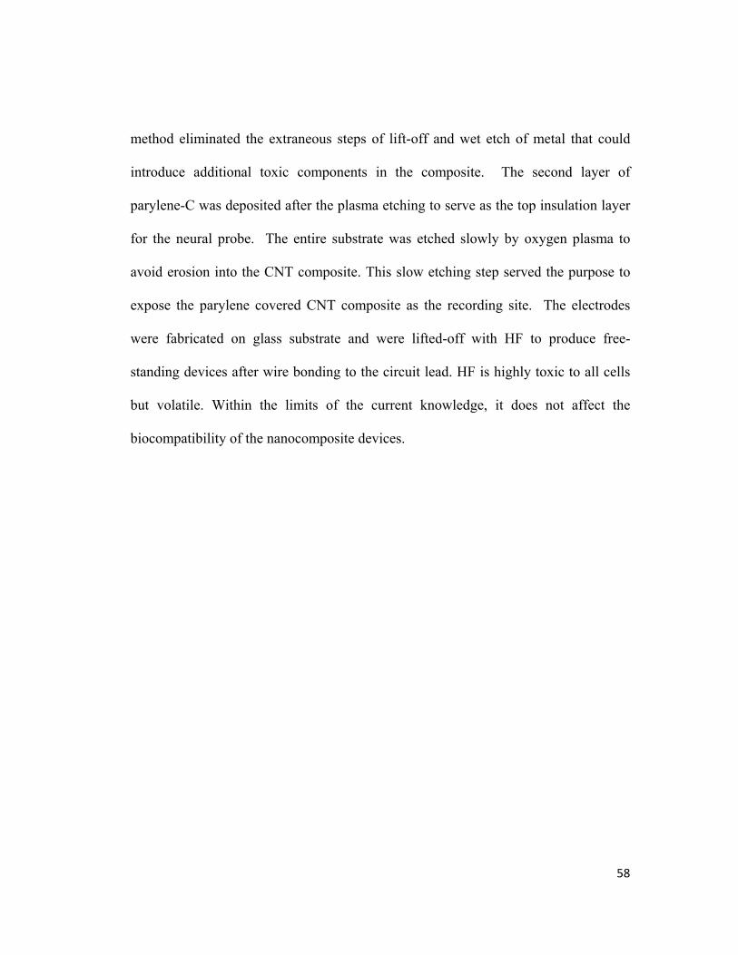
method eliminated the extraneous steps of lift-off and wet etch of metal that could
introduce additional toxic components in the composite. The second layer of
parylene-C was deposited after the plasma etching to serve as the top insulation layer
for the neural probe. The entire substrate was etched slowly by oxygen plasma to
avoid erosion into the CNT composite. This slow etching step served the purpose to
expose the parylene covered CNT composite as the recording site. The electrodes
were fabricated on glass substrate and were lifted-off with HF to produce free-
standing devices after wire bonding to the circuit lead. HF is highly toxic to all cells
but volatile. Within the limits of the current knowledge, it does not affect the
biocompatibility of the nanocomposite devices.
58
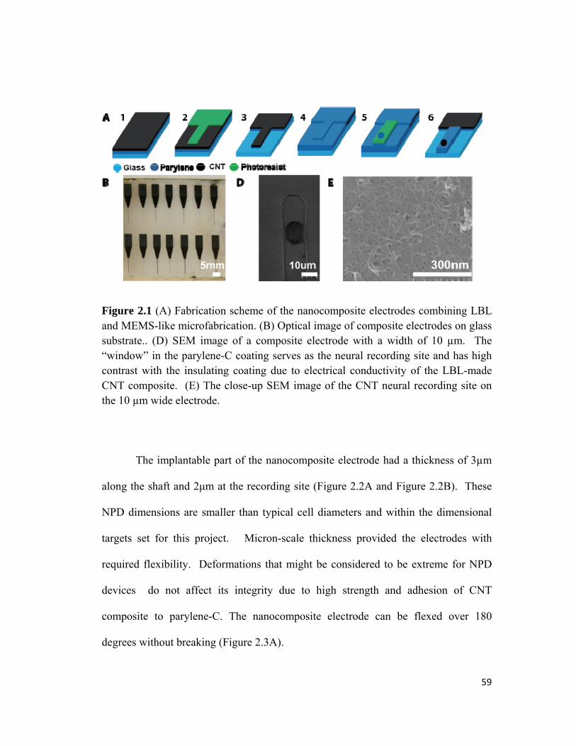
Figure 2.1 (A) Fabrication scheme of the nanocomposite electrodes combining LBL and MEMS-like microfabrication. (B) Optical image of composite electrodes on glass substrate.. (D) SEM image of a composite electrode with a width of 10 µm. The “window” in the parylene-C coating serves as the neural recording site and has high contrast with the insulating coating due to electrical conductivity of the LBL-made CNT composite. (E) The close-up SEM image of the CNT neural recording site on the 10 µm wide electrode.
The implantable part of the nanocomposite electrode had a thickness of 3µm
along the shaft and 2μm at the recording site (Figure 2.2A and Figure 2.2B). These
NPD dimensions are smaller than typical cell diameters and within the dimensional
targets set for this project. Micron-scale thickness provided the electrodes with
required flexibility. Deformations that might be considered to be extreme for NPD
devices do not affect its integrity due to high strength and adhesion of CNT
composite to parylene-C. The nanocomposite electrode can be flexed over 180
degrees without breaking (Figure 2.3A).
59
The width of the electrode is the second dimension that would be desirable to
reduce to sizes comparable to that of a neuron. Here we varied the width of the
electrodes in three sizes: 10 μm, 25 μm, and 50 μm. The smaller versions of the
composite NPDs are within the desirable size range and dimensional targets for NPD
width. They are equal or comparable to the smallest implantable electrodes reported
so far.20, 46,42 Our electrodes are also considerably smaller than other silicon based
devices.8, 9 The high strength of the LBL composites without high bending stiffness
will facilitate their further miniaturization.
The recording sites were varied between three different sizes: ca 100 μm2 , ca
625 μm2, and ca 2500 μm2 depending on the width of the implant. The examination
of the micromanufactured NPDs by scanning electron microscopy (SEM, Figure 1D)
showed that the 100 μm2 recording site at the tip of the electrode was highly
conductive while the rest of the composite electrode was insulated by parylene-C. A
zoomed-in image of the recording site showed that the integrity of the CNT
composite is preserved through the fabrication process (Figure 2.1E).
The total length of the shaft of the micromanufactured electrode was 5000 μm
(Figure 2.1B) which is sufficient to reach deep structures within the rat and human
brain. For comparison the depth of the motor cortex in rats is 5000 μm,49 while the
same for humans is 20000 μm.49 Depending on the clinical purposes of neural
recording, the smaller depths of implantation could be targeted and even preferred as
well.
60
Figure 2.2 (A) ) Cross-section SEM image of the fabricated electrodes (B) Cross-section SEM image of the recording site on the fabricated electrodes. Distortion of the parylene-C and composite layers of the device occurs due to sheer stress due to cutting. Note no delamination of CNT composite layer can be observed.
2.4.2 Mechanical properties
61
After successful fabrication of the electrodes, mechanical tests were
performance to understand better the mechanical properties of the micromanufactured
neural electrode (Figure 2.3B). The complete analysis will require detailed finite
element modeling of the system consisting of hard beam with rectangular or
cylindrical cross-section in a soft matrix for different deformations as well as for
vibrations; which should be subject of a separate study. Here we suggest a simplified
version of evaluation of mechanical compliance based on the mechanical damage of
to the tissues upon deformations to the implant that is reflective of the chronic BBB
trauma around implants. In this approximation, we describe mechanical compliance
with brain tissue by comparing the pressure associated with buckling deformation of
the implant and the critical rupture strength. If the pressure from the brain to buckle
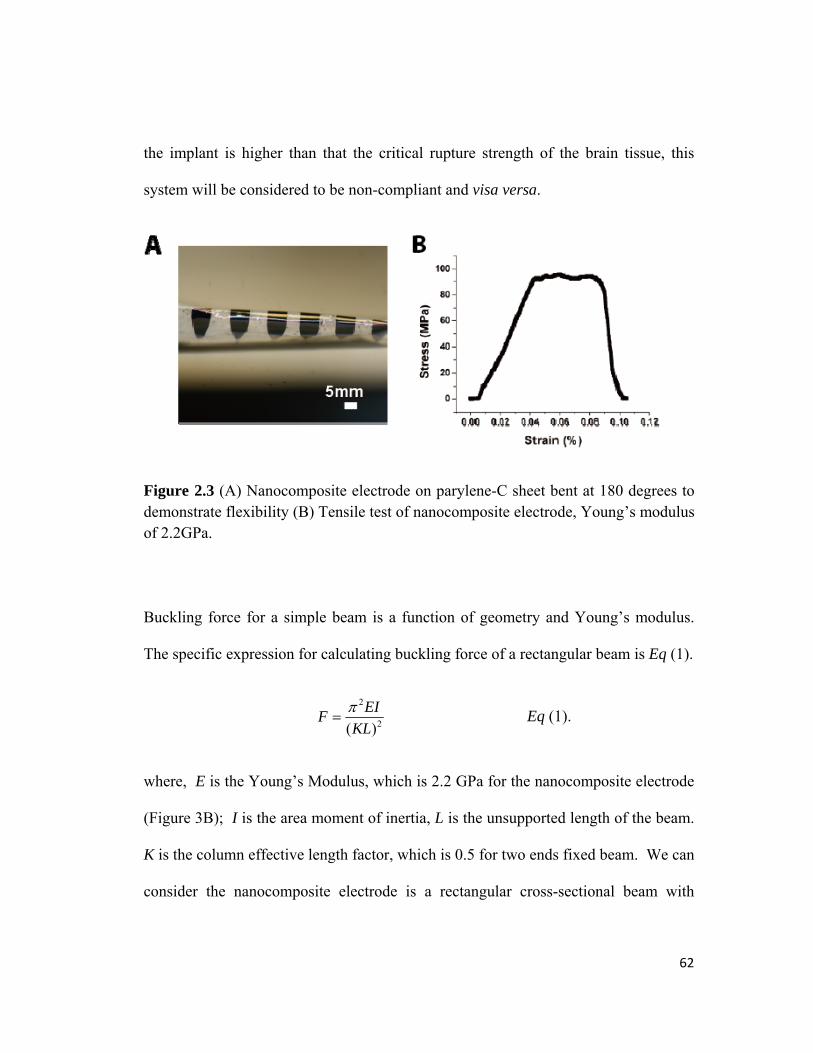
the implant is higher than that the critical rupture strength of the brain tissue, this
system will be considered to be non-compliant and visa versa.
Figure 2.3 (A) Nanocomposite electrode on parylene-C sheet bent at 180 degrees to demonstrate flexibility (B) Tensile test of nanocomposite electrode, Young’s modulus of 2.2GPa.
Buckling force for a simple beam is a function of geometry and Young’s modulus.
The specific expression for calculating buckling force of a rectangular beam is Eq (1).
2
2
)(KLEIF π
= Eq (1).
where, E is the Young’s Modulus, which is 2.2 GPa for the nanocomposite electrode
(Figure 3B); I is the area moment of inertia, L is the unsupported length of the beam.
K is the column effective length factor, which is 0.5 for two ends fixed beam. We can
consider the nanocomposite electrode is a rectangular cross-sectional beam with
62
dimensions of 5000 µm in length, 3 µm in height, and 10 µm in width. For this
geometry, the area moment of inertia is:
12
3whI = Eq (2).
where, h is the height and w is the width. We can calculate the force required for the
electrode to buckle and convert this force to a pressure term by considering the
footprint of the electrodes. This pressure is about 2.37kPa for the nanocomposite
electrode. It is smaller than the critical rupture strength of the brain tissue, which is
typical about 3 kPa.50 This indicated that the composite electrode will likely deform
before inducing the brain tissue rupture.
2.4.3 Electrical Properties
We evaluated their electrochemical performance in terms of impedance (Z)
and charge storage capacity (CSC) measured in a three-electrode electrochemical set-
up and calculated with a custom MATLAB (Mathworks Inc., MA) script. The exact
Z and CSC needed for NPDs depend on neural tissues and the type of the projected
treatment/interface.27 Nevertheless, the minimization of Z and maximization of CSC
are the typical requirements for implantable electrodes as they reflect the key
electrochemical parameters for their reduction of noise in NPDs, reduction of
electrical damage to the tissue, and improving their long-term performance.
Impedance was measured by a frequency response analyzer from 10 Hz to 32 kHz for 63
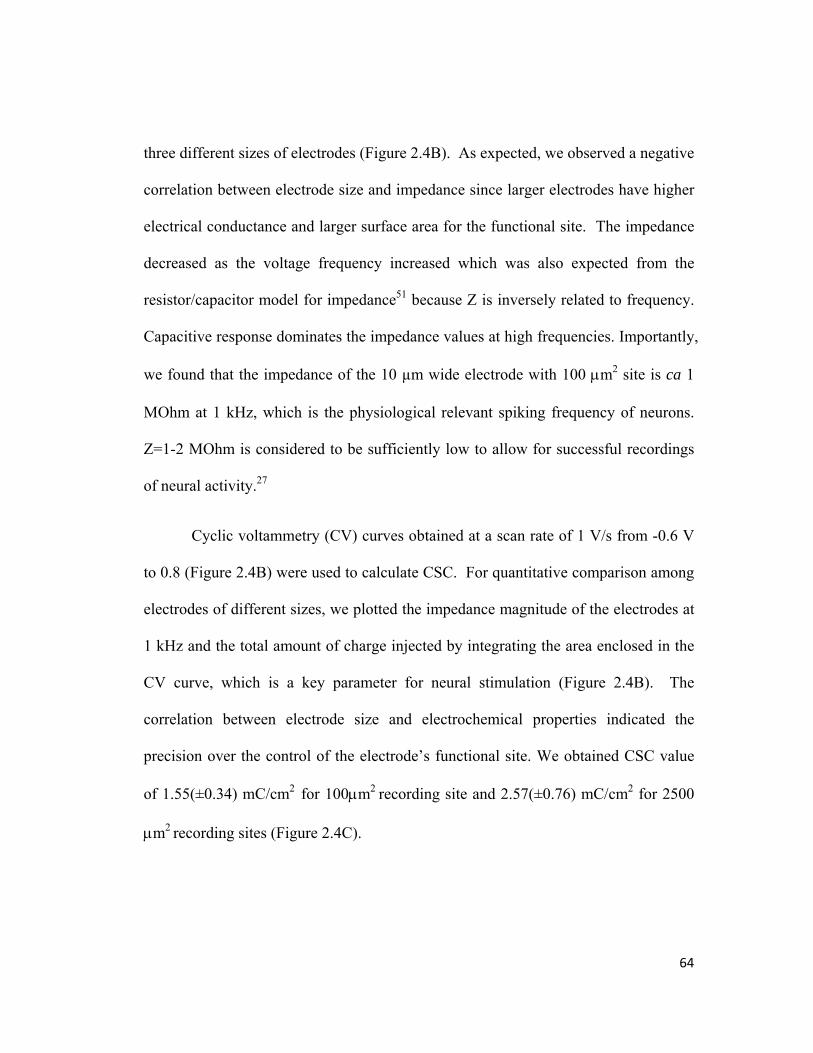
three different sizes of electrodes (Figure 2.4B). As expected, we observed a negative
correlation between electrode size and impedance since larger electrodes have higher
electrical conductance and larger surface area for the functional site. The impedance
decreased as the voltage frequency increased which was also expected from the
resistor/capacitor model for impedance51 because Z is inversely related to frequency.
Capacitive response dominates the impedance values at high frequencies. Importantly,
we found that the impedance of the 10 µm wide electrode with 100 μm2 site is ca 1
MOhm at 1 kHz, which is the physiological relevant spiking frequency of neurons.
Z=1-2 MOhm is considered to be sufficiently low to allow for successful recordings
of neural activity.27
Cyclic voltammetry (CV) curves obtained at a scan rate of 1 V/s from -0.6 V
to 0.8 (Figure 2.4B) were used to calculate CSC. For quantitative comparison among
electrodes of different sizes, we plotted the impedance magnitude of the electrodes at
1 kHz and the total amount of charge injected by integrating the area enclosed in the
CV curve, which is a key parameter for neural stimulation (Figure 2.4B). The
correlation between electrode size and electrochemical properties indicated the
precision over the control of the electrode’s functional site. We obtained CSC value
of 1.55(±0.34) mC/cm2 for 100μm2 recording site and 2.57(±0.76) mC/cm2 for 2500
μm2 recording sites (Figure 2.4C).
64
Figure 2.4(A) Typical impedance (Z) of the electrodes with different sizes of the functional sites. (B) Typical cyclic voltammetry of the electrodes with different sizes of the functional sites, sweep from 0.8 V to -0.6 V at 1V/s scan rate. (C) Cumulative electrochemical properties of the nanocomposite electrodes. Eight electrodes were tested for each size.
2.4.4 Surgical Procedure
As expected, the softness and flexibility of the nanocomposite electrodes
became a major challenge during the electrode insertion into the brain. Several
methods were considered to circumvent the problem of insertion of a soft rod into soft
matrix, such as using water-soluble polymers to temporarily stiffen the probes52 and
chemically modified probe-releasing shuttles.53 The use of stiffening materials was
not favored by us because they (a) inherently restricts the size of implant to those that
can perform as stiff rods, which limits the possibilities of microminiaturization; (b)
remnants of the polymers can cause inflammation; and (c) if products of
biodegradation of such polymers remain at the NPD-tissue interface, they will
increase interfacial impedance Z.
65
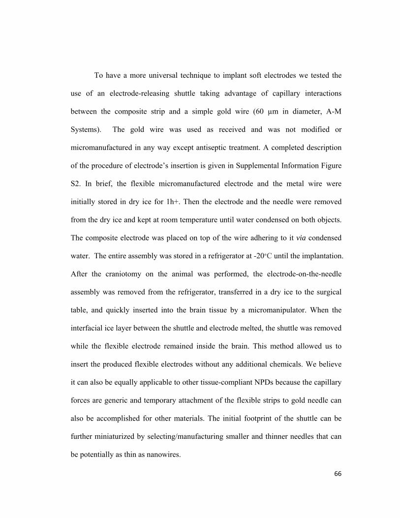
To have a more universal technique to implant soft electrodes we tested the
use of an electrode-releasing shuttle taking advantage of capillary interactions
between the composite strip and a simple gold wire (60 µm in diameter, A-M
Systems). The gold wire was used as received and was not modified or
micromanufactured in any way except antiseptic treatment. A completed description
of the procedure of electrode’s insertion is given in Supplemental Information Figure
S2. In brief, the flexible micromanufactured electrode and the metal wire were
initially stored in dry ice for 1h+. Then the electrode and the needle were removed
from the dry ice and kept at room temperature until water condensed on both objects.
The composite electrode was placed on top of the wire adhering to it via condensed
water. The entire assembly was stored in a refrigerator at -20°C until the implantation.
After the craniotomy on the animal was performed, the electrode-on-the-needle
assembly was removed from the refrigerator, transferred in a dry ice to the surgical
table, and quickly inserted into the brain tissue by a micromanipulator. When the
interfacial ice layer between the shuttle and electrode melted, the shuttle was removed
while the flexible electrode remained inside the brain. This method allowed us to
insert the produced flexible electrodes without any additional chemicals. We believe
it can also be equally applicable to other tissue-compliant NPDs because the capillary
forces are generic and temporary attachment of the flexible strips to gold needle can
also be accomplished for other materials. The initial footprint of the shuttle can be
further miniaturized by selecting/manufacturing smaller and thinner needles that can
be potentially as thin as nanowires.
66
Figure 2.5 Schematic of the electrode/shuttle system
2.4.5 Post-Surgery Imaging:
To assess the integrity of the electrode after the implantation and its resilience
to shear forces during the surgery we removed the electrode from the brain and
investigated the cross-section of the implanted electrode by SEM (Figure 2.6G). As
one can see the structure of the device was well-preserved and no obvious
delamination of neither the top or the bottom layer of the electrode occurred.
Several aspects of implantation method need further evaluation for its routine
usage, such as the effect of the initial low temperature condition to the brain, sterile
condition of the ambient condensed water, and initial acute damage from the shuttle.
Here we made a preliminary investigation of the tissue damage induced by the
procedure using ex vivo by confocal microcopy. The electrode was green stained with
FITC-albumin solution prior to implantation (Figure 2.6F); the brain tissue cells were
stained with toluidine blue having red luminescence after electrode implantation. We
67
observed concentration of brain cells close to the electrode (bright red emission). The
size of this particular area is similar to the shuttle footprint (50µm). It is possibly
because the shuttle insertion damaged extracellular matrix and packed brain cells
close together. Alternatively, the same imaging effect could be associate the cellular
damage that is reflected by the higher permeability of the dye. The effect of this
damage on the long-term functionality of the CNT electrodes and its relationship to
chronic inflammation will require further study.
In addition to trauma assessment, non-invasive and label-free imaging
techniques are important to guide/monitor the electrode through different stages of
the implantation.54 In this study, the state of the electrodes after implantation was
examined by two imaging modalities ex vivo: photoacoustic microscopy (PAM)55, 56
and magnetic resonance imaging (MRI).
Prior to electrode insertion and after craniotomy, one needs to closely assess
the insertion site to identify the specific region of interest and also avoid blood
vessels to minimize bleeding and BBB trauma. PAM combines optical and acoustic
imaging techniques to produce images with excellent optical contrast and great
imaging depth. This technique is based on the difference of optical absorption in
tissues and was realized by rastering laser beam over the brain tissue (Figure 2.6A). It
offers higher imaging depth than optical microscopy, and provides the same
functional information. It would be an excellent tool for monitoring vasculature
within the region of the interest. In our specific set up, photoacoustic signals were
68
detected by a calibrated needle hydrophone and the ultrasound coupling was through
water. With this imaging system, we can achieve lateral resolution of 5 µm and axial
resolution of 100 µm. Figure 3B represents a surface PAM image of the
nanocomposite electrode inserted into the brain tissue. Due to its strong optical
absorption, the nanocomposite electrodes displayed high contrast in the image, which
is the portion of the electrode outside of the brain in Figure 2.6B. CNT electrodes
were curved from the sided due to its flexibility, and we purposefully curved the
particular part of the electrode to observe where the electrode was inserted. Moreover,
we could also visualize the vasculature near the brain surface due to strong absorption
of hemoglobin. Three dimensional mapping of the blood vessels is very important for
electrode insertion. PAM makes possible high resolution mapping of blood vessels in
the brain tissue which can be utilized to minimize their rupture during the insertion
procedure, thus reducing insertion trauma, and preserving neurons. Combining
electrodes with high PAM contrast image of blood vessels could be a valuable tool
for clinical neural surgery.
Assessing implanted flexible neural electrodes inside of the brain during and
after the surgery is also crucial,54 especially after the electrodes were closely sealed
inside of the skull. MRI is a well-established technique that can provide a non-
invasive and high depth 3D image of the nanocomposite electrodes inside the brain.57
It could monitor precisely the position of the electrode with the skull intact. We
acquired MRI images after implanting the compliant electrode from nanotubes
(Figure 2.6C-E). The high contrast of the nanocomposite electrode is attributed to 69
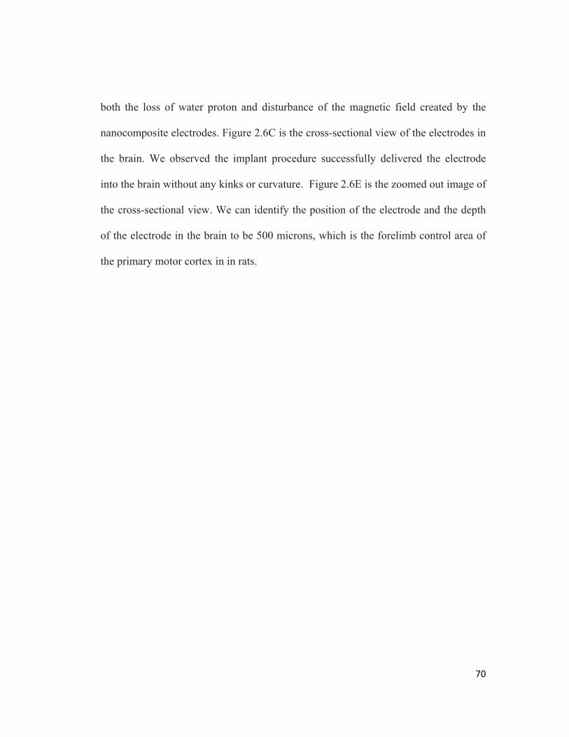
both the loss of water proton and disturbance of the magnetic field created by the
nanocomposite electrodes. Figure 2.6C is the cross-sectional view of the electrodes in
the brain. We observed the implant procedure successfully delivered the electrode
into the brain without any kinks or curvature. Figure 2.6E is the zoomed out image of
the cross-sectional view. We can identify the position of the electrode and the depth
of the electrode in the brain to be 500 microns, which is the forelimb control area of
the primary motor cortex in in rats.
70
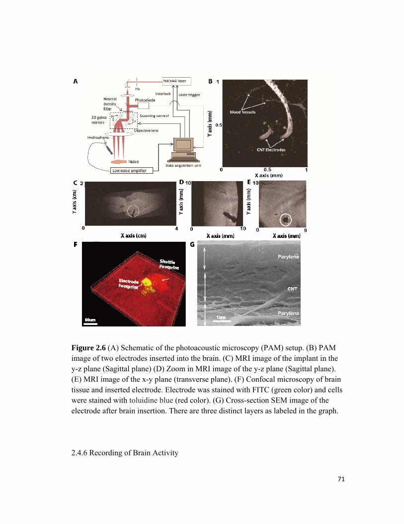
Figure 2.6 (A) Schematic of the photoacoustic microscopy (PAM) setup. (B) PAM image of two electrodes inserted into the brain. (C) MRI image of the implant in the y-z plane (Sagittal plane) (D) Zoom in MRI image of the y-z plane (Sagittal plane). (E) MRI image of the x-y plane (transverse plane). (F) Confocal microscopy of brain tissue and inserted electrode. Electrode was stained with FITC (green color) and cells were stained with toluidine blue (red color). (G) Cross-section SEM image of the electrode after brain insertion. There are three distinct layers as labeled in the graph.
2.4.6 Recording of Brain Activity
71
After verifying the electrochemical performance of the as-fabricated neural
electrodes and carefully assessing the state of the neural electrodes, we conducted in
vivo physiological recording experiments with rats. The typical procedure of the
animal preparation and neural recording was published previously9 and described in
the methods section. The neural electrode with 100 um2 recoding site was inserted
into the brain tissue as described in the previous paragraph. Total of four electrodes
were inserted into four different animals. Acute neural recording were conducted
immediately after electrode insertion. Figure 2.7C is the typical low frequency neural
signal recorded over time. The color spectrum of the plot represents the intensity of
the local field potential. We observed high signal intensity (dark red color) in the low
frequency range (0 to 20 Hz) over the entire recording session. We concluded that the
electrode can record low frequency signal consistently over time. To further identify
the peak of the low frequency neural recording, we accumulated the intensity data
over time to generate a power spectrum. The power spectrum showed a peak around
5 Hz. We did not observe any intensity peak at 60 Hz, which is common for
instrumental background noise. The power spectrum clearly demonstrated that the
neural electrode could specifically identify the low frequency neural signal from
instrumental noise (Figure 2.6C). Furthermore, we conducted a blank recording
experiment in buffer saline solution. We observed much lower signal power compare
to the recoding in the animal brain (Figure 2.7D and Figure 2.7E). We did not observe
single neural spike in our recording session, it is possibly due to the effect of
isoflurane.
72

Figure 2.7 (A) Harvested animal brain after recording experiment. (B) Low frequency signal recorded from the brain with the 10 µm wide nanocomposite electrode (100μm2 recording site) (C) Power spectrum of the low frequency signal recording, signal peak at 5 Hz. . Blank recording experiment in phosphate buffered saline (PBS) (D) Local field potential recorded from PBS. (E) Power Spectrum of the recorded local field potential.
2.4 Conclusions
This study demonstrated that LBL assembly is capable of producing tissue-
compliant CNT nanocomposites with electrochemical performance particularly
suitable for neuroprosthetic devices. These composites can be microfabricated with
required precision using standard photolithography technology into flexible neural 73

electrodes. The footprint of the electrodes can be miniaturized to 10 µm in width
with thicknesses as small as 3µm, which is smaller than any stiff18 or flexible50
functional NPDs reported to date. Importantly, the process of implantation of such
compliant devices was developed which could be applied to other devices with
similar mechanical properties made from nanocomposites or other suitable materials
satisfying conditions discussed above. We want to point out that better understanding
of the mechanics of the flexible brain implants in soft brain tissue, and therefore,
requirements to the materials used in neuroprosthetic devices is needed.
The low frequency neural signal was recorded in the animal model to
demonstrate the functionality of the neural electrodes. Further exploration of high
frequency recordings of neuronal signals and microfabrication of arrays of tissue
compliant electrodes is necessary. The ability to record high frequency signals and
single neuronal activity require changes in electrode design. Similarly to our
previous study,18 the evaluation of the chronic tissue response should also be carried
out to demonstrate the long-term functionality and inflammation response of this new
class of nanocomposite electrodes. We also utilized both emerging and well
established imaging modalities to examine these flexible neural electrodes in the
brain. In aggregate the results reported in this paper takes us a step further to the use
of nanocomposite-based neural prosthetics in clinical setting.
74
2.6 References
1. Kennedy, P. R.; Bakay, R. A., Restoration of Neural Output from a Paralyzed
Patient by a Direct Brain Connection. Neuroreport 1998, 9, 1707-11.
2. Donoghue, J. P., Connecting Cortex to Machines: Recent Advances in Brain
Interfaces. Nat Neurosci 2002, 5 Suppl, 1085-8.
3. Callaghan, J. C., Early Experiences in the Study and Development of an
Artificial Electrical Pacemaker for Standstill of the Heart: View from 1949. Pacing
Clin Electrophysiol 1980, 3, 618-9.
4. Hochberg, L. R.; Serruya, M. D.; Friehs, G. M.; Mukand, J. A.; Saleh, M.;
Caplan, A. H.; Branner, A.; Chen, D.; Penn, R. D.; Donoghue, J. P., Neuronal
Ensemble Control of Prosthetic Devices by a Human with Tetraplegia. Nature 2006,
442, 164-71.
5. Strumwasser, F., Long-Term Recording' from Single Neurons in Brain of
Unrestrained Mammals. Science 1958, 127, 469-70.
6. Ellis, T. L.; Stevens, A., Deep Brain Stimulation for Medically Refractory
Epilepsy. Neurosurgical focus 2008, 25, E11.
7. Rousche, P. J.; Normann, R. A., Chronic Recording Capability of the Utah
Intracortical Electrode Array in Cat Sensory Cortex. Journal of neuroscience methods
1998, 82, 1-15.
8. Campbell, P. K.; Jones, K. E.; Huber, R. J.; Horch, K. W.; Normann, R. A., A
Silicon-Based, Three-Dimensional Neural Interface: Manufacturing Processes for an
75
Intracortical Electrode Array. IEEE transactions on bio-medical engineering 1991, 38,
758-68.
9. Ludwig, K. A.; Uram, J. D.; Yang, J.; Martin, D. C.; Kipke, D. R., Chronic
Neural Recordings Using Silicon Microelectrode Arrays Electrochemically Deposited
with a Poly(3,4-Ethylenedioxythiophene) (Pedot) Film. J Neural Eng 2006, 3, 59-70.
10. Ward, M. P.; Rajdev, P.; Ellison, C.; Irazoqui, P. P., Toward a Comparison of
Microelectrodes for Acute and Chronic Recordings. Brain research 2009, 1282, 183-
200.
11. Biran, R.; Martin, D. C.; Tresco, P. A., Neuronal Cell Loss Accompanies the
Brain Tissue Response to Chronically Implanted Silicon Microelectrode Arrays. Exp
Neurol 2005, 195, 115-26.
12. Edell, D. J.; Toi, V. V.; McNeil, V. M.; Clark, L. D., Factors Influencing the
Biocompatibility of Insertable Silicon Microshafts in Cerebral Cortex. IEEE
transactions on bio-medical engineering 1992, 39, 635-43.
13. Fawcett, J. W.; Asher, R. A., The Glial Scar and Central Nervous System
Repair. Brain research bulletin 1999, 49, 377-91.
14. Subbaroyan, J.; Martin, D. C.; Kipke, D. R., A Finite-Element Model of the
Mechanical Effects of Implantable Microelectrodes in the Cerebral Cortex. J Neural
Eng 2005, 2, 103-13.
15. Discher, D. E.; Janmey, P.; Wang, Y.-l., Tissue Cells Feel and Respond to the
Stiffness of Their Substrate. Science 2005, 310, 1139-1143.
76
16. Keohan, F.; Wei, X. F.; Wongsarnpigoon, A.; Lazaro, E.; Darga, J. E.; Grill,
W. M., Fabrication and Evaluation of Conductive Elastomer Electrodes for Neural
Stimulation. J Biomater Sci Polym Ed 2007, 18, 1057-73.
17. Seymour, J. P.; Kipke, D. R., Neural Probe Design for Reduced Tissue
Encapsulation in Cns. Biomaterials 2007, 28, 3594-607.
18. Kim, Y. T.; Hitchcock, R. W.; Bridge, M. J.; Tresco, P. A., Chronic Response
of Adult Rat Brain Tissue to Implants Anchored to the Skull. Biomaterials 2004, 25,
2229-2237.
19. Sanders, J. E.; Stiles, C. E.; Hayes, C. L., Tissue Response to Single-Polymer
Fibers of Varying Diameters: Evaluation of Fibrous Encapsulation and Macrophage
Density. J Biomed Mater Res 2000, 52, 231-7.
20. Kozai, T. D.; Langhals, N. B.; Patel, P. R.; Deng, X.; Zhang, H.; Smith, K. L.;
Lahann, J.; Kotov, N. A.; Kipke, D. R., Ultrasmall Implantable Composite
Microelectrodes with Bioactive Surfaces for Chronic Neural Interfaces. Nature
materials 2012, 11, 1065-73.
21. Hai, A.; Shappir, J.; Spira, M. E., In-Cell Recordings by Extracellular
Microelectrodes. Nat Methods 2010, 7, 200-2.
22. Rousche, P. J.; Pellinen, D. S.; Pivin, D. P., Jr.; Williams, J. C.; Vetter, R. J.;
Kipke, D. R., Flexible Polyimide-Based Intracortical Electrode Arrays with Bioactive
Capability. IEEE transactions on bio-medical engineering 2001, 48, 361-71.
77
23. Seo, J.-M.; Kim, S. J.; Chung, H.; Kim, E. T.; Yu, H. G.; Yu, Y. S.,
Biocompatibility of Polyimide Microelectrode Array for Retinal Stimulation.
Materials Science and Engineering: C 2004, C24, 185-189.
24. Boppart, S. A.; Wheeler, B. C.; Wallace, C. S., A Flexible Perforated
Microelectrode Array for Extended Neural Recordings. IEEE transactions on bio-
medical engineering 1992, 39, 37-42.
25. Cogan, S. F.; Ehrlich, J.; Plante, T. D.; Van Wagenen, R., Penetrating
Microelectrode Arrays with Low-Impedance Sputtered Iridium Oxide Electrode
Coatings. Conference proceedings : ... Annual International Conference of the IEEE
Engineering in Medicine and Biology Society. IEEE Engineering in Medicine and
Biology Society. Conference 2009, 2009, 7147-50.
26. Gheith, M. K.; Pappas, T. C.; Liopo, A. V.; Sinani, V. A.; Shim, B. S.;
Motamedi, M.; Wicksted, J. P.; Kotov, N. A., Stimulation of Neural Cells by Lateral
Currents in Conductive Layer-by-Layer Films of Single-Walled Carbon Nanotubes.
Adv Mater 2006, 18, 2975-2979.
27. Cogan, S. F., Neural Stimulation and Recording Electrodes. Annu Rev Biomed
Eng 2008, 10, 275-309.
28. Kotov, N. A.; Winter, J. O.; Clements, I. P.; Jan, E.; Timko, B. P.; Campidelli,
S.; Pathak, S.; Mazzatenta, A.; Lieber, C. M.; Prato, M.; Bellamkonda, R. V.; Silva, G.
A.; Kam, N. W. S.; Patolsky, F.; Ballerini, L., Nanomaterials for Neural Interfaces.
Adv Mater 2009, 21, 3970-4004.
78
29. Malarkey, E. B.; Parpura, V., Carbon Nanotubes in Neuroscience. Act Neur S
2010, 106, 337-341.
30. Jan, E.; Hendricks, J. L.; Husaini, V.; Richardson-Burns, S. M.; Sereno, A.;
Martin, D. C.; Kotov, N. A., Layered Carbon Nanotube-Polyelectrolyte Electrodes
Outperform Traditional Neural Interface Materials. Nano letters 2009, 9, 4012-8.
31. Luo, X.; Weaver, C. L.; Zhou, D. D.; Greenberg, R.; Cui, X. T., Highly Stable
Carbon Nanotube Doped Poly(3,4-Ethylenedioxythiophene) for Chronic Neural
Stimulation. Biomaterials 2011, 32, 5551-7.
32. Shim, B. S.; Zhu, J.; Jan, E.; Critchley, K.; Ho, S.; Podsiadlo, P.; Sun, K.;
Kotov, N. A., Multiparameter Structural Optimization of Single-Walled Carbon
Nanotube Composites: Toward Record Strength, Stiffness, and Toughness. ACS Nano
2009, 3, 1711-1722.
33. Shao, M. W.; Wang, D. B.; Yu, G. H.; Hu, B.; Yu, W. C.; Qian, Y. T., The
Synthesis of Carbon Nanotubes at Low Temperature Via Carbon Suboxide
Disproportionation. Carbon 2004, 42, 183-185.
34. Lin, C. M.; Lee, Y. T.; Yeh, S. R.; Fang, W. L., Flexible Carbon Nanotubes
Electrode for Neural Recording. Biosens Bioelectron 2009, 24, 2791-2797.
35. Zhou, Y. X.; Hu, L. B.; Gruner, G., A Method of Printing Carbon Nanotube
Thin Films. Appl Phys Lett 2006, 88.
36. Abadi, P. P. S. S.; Hutchens, S. B.; Greer, J. R.; Cola, B. A.; Graham, S.,
Buckling-Driven Delamination of Carbon Nanotube Forests. Appl Phys Lett 2013,
102, 223103.
79
37. Shim, B. S.; Zhu, J. A.; Jan, E.; Critchley, K.; Kotov, N. A., Transparent
Conductors from Layer-by-Layer Assembled Swnt Films: Importance of Mechanical
Properties and a New Figure of Merit. ACS Nano 2010, 4, 3725-3734.
38. Zhu, J.; Shim, B. S.; Di Prima, M.; Kotov, N. A., Transparent Conductors
from Carbon Nanotubes Lbl-Assembled with Polymer Dopant with Pi-Pi Electron
Transfer. J Am Chem Soc 2011, 133, 7450-7460.
39. Kam, N. W. S.; Jan, E.; Kotov, N. A., Electrical Stimulation of Neural Stem
Cells Mediated by Humanized Carbon Nanotube Composite Made with Extracellular
Matrix Protein. Nano letters 2009, 9, 273-278.
40. Jan, E.; Kotov, N. A., Successful Differentiation of Mouse Neural Stem Cells
on Layer-by-Layer Assembled Single-Walled Carbon Nanotube Composite. Nano
letters 2007, 7, 1123-1128.
41. Lovat, V.; Pantarotto, D.; Lagostena, L.; Cacciari, B.; Grandolfo, M.; Righi,
M.; Spalluto, G.; Prato, M.; Ballerini, L., Carbon Nanotube Substrates Boost
Neuronal Electrical Signaling. Nano letters 2005, 5, 1107-10.
42. Malarkey, E. B.; Fisher, K. A.; Bekyarova, E.; Liu, W.; Haddon, R. C.;
Parpura, V., Conductive Single-Walled Carbon Nanotube Substrates Modulate
Neuronal Growth. Nano letters 2009, 9, 264-268.
43. Cellot, G.; Cilia, E.; Cipollone, S.; Rancic, V.; Sucapane, A.; Giordani, S.;
Gambazzi, L.; Markram, H.; Grandolfo, M.; Scaini, D.; Gelain, F.; Casalis, L.; Prato,
M.; Giugliano, M.; Ballerini, L., Carbon Nanotubes Might Improve Neuronal
Performance by Favouring Electrical Shortcuts. Nat Nanotechnol 2009, 4, 126-133.
80
44. Wang, X.; Xie, X.; Ku, G.; Wang, L. V.; Stoica, G., Noninvasive Imaging of
Hemoglobin Concentration and Oxygenation in the Rat Brain Using High-Resolution
Photoacoustic Tomography. Journal of biomedical optics 2006, 11, 024015.
45. Keefer, E. W.; Botterman, B. R.; Romero, M. I.; Rossi, A. F.; Gross, G. W.,
Carbon Nanotube Coating Improves Neuronal Recordings. Nat Nanotechnol 2008, 3,
434-9.
46. Yoon, I.; Hamaguchi, K.; Borzenets, I. V.; Finkelstein, G.; Mooney, R.;
Donald, B. R., Intracellular Neural Recording with Pure Carbon Nanotube Probes.
PLoS ONE 2013, 8, e65715.
47. Jan, E.; Byrne, S. J.; Cuddihy, M.; Davies, A. M.; Volkov, Y.; Gun'ko, Y. K.;
Kotov, N. A., High-Content Screening as a Universal Tool for Fingerprinting of
Cytotoxicity of Nanoparticles. ACS Nano 2008, 2, 928-938.
48. Stieglitz, T., Hansjorg, B., Schuettler, M. and Meyer, J.-U, Micromachined,
Polyimide-Based Devices for Flexible Neural Interfaces. Biomedical Microdevices
2000, 2, 283-294.
49. Kandel, E. R.; Schwartz, J. H.; Jessell, T. M., Principles of Neural Science.
4th ed.; McGraw-Hill, Health Professions Division: New York, 2000; p xli, 1414 p.
50. Franceschini, G. The Mechanics of Human Brain Tissue University of Trento,
2006.
51. Merrill, D. R.; Bikson, M.; Jefferys, J. G., Electrical Stimulation of Excitable
Tissue: Design of Efficacious and Safe Protocols. Journal of neuroscience methods
2005, 141, 171-98.
81
82
52. Fan, W.; Maesoon, I.; Euisik, Y. In A Flexible Fish-Bone-Shaped Neural
Probe Strengthened by Biodegradable Silk Coating for Enhanced Biocompatibility,
Solid-State Sensors, Actuators and Microsystems Conference (TRANSDUCERS),
2011 16th International, 5-9 June 2011; 2011; pp 966-969.
53. Kozai, T. D.; Kipke, D. R., Insertion Shuttle with Carboxyl Terminated Self-
Assembled Monolayer Coatings for Implanting Flexible Polymer Neural Probes in
the Brain. Journal of neuroscience methods 2009, 184, 199-205.
54. Kozai, T. D.; Vazquez, A. L.; Weaver, C. L.; Kim, S. G.; Cui, X. T., In Vivo
Two-Photon Microscopy Reveals Immediate Microglial Reaction to Implantation of
Microelectrode through Extension of Processes. J Neural Eng 2012, 9, 066001.
55. Hu, S.; Maslov, K.; Wang, L. V., Second-Generation Optical-Resolution
Photoacoustic Microscopy with Improved Sensitivity and Speed. Opt Lett 2011, 36,
1134-6.
56. Xie, Z.; Jiao, S.; Zhang, H. F.; Puliafito, C. A., Laser-Scanning Optical-
Resolution Photoacoustic Microscopy. Opt Lett 2009, 34, 1771-3.
57. Aine, C. J., A Conceptual Overview and Critique of Functional Neuroimaging
Techniques in Humans: I. Mri/Fmri and Pet. Crit Rev Neurobiol 1995, 9, 229-309.
83
Chapter 3
Gold Nanoparticles for Neural Prosthetic Devices
3.1 Abstract
Treatments of neurological diseases and the realization of brain-computer
interfaces require ultrasmall electrodes which are “invisible” to resident immune cells.
Functional electrodes smaller than 50μm are impossible to produce with traditional
materials due to high interfacial impedance at the characteristic frequency of neural
activity and insufficient charge storage capacity. The problem can be resolved by
using gold nanoparticle nanocomposites. Careful comparison indicates that layer-by-
layer assembled films from Au NPs provide more than three-fold improvement in
interfacial impedance and one order of magnitude increase in charge storage capacity.
Prototypes of microelectrodes could be made using traditional photolithography.
Integration of unique nanocomposite materials with microfabrication techniques
84
opens the door for practical realization of the ultrasmall implantable electrodes.
Further improvement of electrical properties is expected when using special shapes of
gold nanoparticles.
3.2 Introduction
Neural prosthetic devices (NPDs), like artificial pacemakers1 and cochlear
implants2 are becoming increasingly relevant for the diagnosis and treatments of
many neurological conditions and traumas. Commonly, these devices utilize
electrodes to interact with neural tissues and achieve targeted stimulation or recording.
For example, chronic deep brain stimulation (DBS) can alleviate symptoms of
Parkinson’s3 and even Alzheimer’s disease.4 NPDs have also allowed patients of
ayomyotrophic lateral sclerosis to regain motor functions.5 Recently, brain-computer
interfaces have received increased attention due to the possibility of using multi-site
recording NPD platforms for restoration of mobility and prosthetic devices for limbs.6,
7 Despite initial clinical successes, there are still many challenges in creating long-
lasting, high-performance neural prosthetic devices.
To improve the long-term stability and performance of current NPDs, it is
necessary to minimize the inflammatory response induced by NPDs. Typically, after
implantation, a layer of scar tissue forms around the NPD due to accumulation of
resident immune cells.8, 9 This layer will create a barrier between the device and the
target neural tissue, which causes the device to lose its functionality overtime.10
85
Studies have suggested that inflammatory response is substantially reduced as
the implant becomes smaller.11, 12 The ideal dimensions of implantable neural
electrodes should not exceed 10 μm in either width or thickness.13 Moreover, it was
demonstrated that subcellular-sized electrodes allow the formation of tight junction
between neurons and electrodes, thus creating effective electrical coupling at the
neuron/electrode interface.14 Mechanical properties of the electrodes are also closely
related to inflammation. Electrodes made of rigid materials, such as noble metals and
semiconductors, have large mismatch in mechanical properties with neural tissues.15,
16 This mismatch becomes particularly significant when considering the inevitable
microscale motion of electrodes relative to the brain tissues.17 This motion triggers
additional immune response through mechanical signal transduction.12 Smaller
flexible electrodes have better compliance with soft tissues and are expected to help
reduce the additional activation of immune pathways and scar formation.
While the concept of ultrasmall flexible electrodes is well understood, the
pathway to its practical realization is not. The ultrasmall electrodes bring up
challenging material issues. The electrical properties of all current classical and
advanced materials exemplified by platinum, doped silicon, polypyrrole, poly(3,4-
ethylenedioxythiophene)(PEDOT), and iridium oxide (IrOx), greatly limit the
functionalities of electrodes smaller than 50-100 μm. The charge storage capacity
(CSC) and interfacial impedance (Z) of these materials are not sufficient to reliably
record signals from electrodes below this size.
86
To resolve these issues, it is necessary to develop new materials with
improved Z and CSC than current materials.18 Lower electrical impedance improves
signal-to-noise ratio and the long-term recording quality of NPDs19, 20 and reduces
harmful overpotential. High CSC materials can deliver a higher charge per area of the
electrodes to the surrounding tissue for neural stimulation. The general strategy for
improving Z and CSC is to increase the electrochemical surface area of the electrodes
for a given geometric surface area.21, 22 Most advanced materials used for neural
electrodes, including platinum black,23 conductive polymer,24 and iridium oxide25
have high-roughness surfaces to increase the ratio of electrochemical surface area and
geometric surface area, consequently improving the Z and CSC. Evidently,
conductive nanomaterials would be ideal for engineering the surfaces of the neural
electrodes.
Currently, most research on nanomaterials for neural interface is mainly
focused on CNT-based material.20, 26-36 It has been demonstrated that CNT coating
improves in vivo neural recording both in rats and primates.20 Despite excellent
mechanical properties of CNT, the electrochemical performance of CNT composites
is still not as high as needed for the ultrasmall NPDs with dimensions ≤10μm.
Biocompatibility and related inflammation processes initiated by electrodes from
CNT or other materials with respect to long-term implantation (on the scale of years)
remains a concern37 that needs to be addressed in the future. These challenges drive
us to explore other nanomaterials and further optimize the electrochemical properties
of neural interface materials.38, 39 Additionally, nanoporous gold and gold
87
nanopowder were also investigated for neural interface applications.22, 40 Both studies
demonstrated the possibility of creating high roughness gold surfaces. However, these
techniques require extensive instrumentation (ultra high vacuum deposition and mold
fabrication) and high processing temperatures.
Solution processed gold nanoparticles (Au NPs) have been studied extensively
for their biological applications.41 They have minimal toxicity,42 are highly
conductive,43 and are very simple to fabricate.44 Au NP/polymer composites have
great potential for NPD applications in term of electrochemical performance and
biocompatibility, but Au NPs have never been used for neural interface applications.
A lot of attention paid to carbon nanotubes (CNT) probably overshadowed Au NPs as
material suitable for neural interface. CNTs were considered a priori to be a better
choice due to their fibrous morphology, high electron mobility, and high surface area.
26 Here we demonstrate that this assumption was probably incorrect and materials
with better electrochemical performance can be made from Au NPs. Measurements of
electrochemical properties on NPD prototypes indicate that in respect to Z and CSC,
Au NP films substantially outperform SWNT composites. Since the microfabrication
process developed here for Au NP composites is compatible with current
microelectrode technology, this study opens the way to a new generation of
implantable electrodes.
3.3 Material and Methods
88
High purity single wall carbon nanotubes (P2-SWNTs) were purchased from
Carbon Solution, Inc. (Riverside, CA), respectively. Poly(vinyl alcohol) (PVA; MW
70k), poly(sodium 4-styrene-sulfonate) (PSS; MW 100k), and
Poly(diallyldimethylammonium chloride) (PDDA)were obtained from Sigma-Aldrich.
All other chemicals were obtained from Sigma-Aldrich
3.3.1 Synthesis of Gold Nanoparticles
The synthesis of Au NPs followed the standard citrate reduction method.
Briefly, 90 mg of HAuCl4 were dissolved in 500 ml of water. The solution was
heated on a hot plate until boiling. Then 25ml of 0.1% sodium citrate aqueous
solution was added to the gold salt solution. The mixture was stirred and reboiled on a
hot plate. After 20 minutes, the solution became a red color, which indicated the
formation of Au NPs. The Au NPs were concentrated 10X by centrifuging at 9000
rpm for 50 minute and removing 90% of the supernatant
3.3.2 Layer-by-Layer Assembly of Au NP film and SWNT film
LbL assembly was initially carried out on microscope glass slides cleaned in
piranha solution overnight and then thoroughly rinsed with deionized water prior to
the use. For LBL assembly, a glass slide was immersed in 0.1 wt % solution of
PDDA for 5 min, rinsed with DI water for 1 min, dried, and then immersed in
89
concentrated Au NP solution for 10 min, rinsed for 1 min, and dried again. The
procedure was then repeated with PDDA and Au NP solution.
SWNTs were first dispersed at 0.5 mg/mL in 2mg/ml PSS (MW 100k)
solution by ultrasonication. 0.1 wt % PVA solution was prepared by dissolving
correct amount of PVA in near boiling water. For each deposition cycle, the
electrode was immersed in the PVA solution for 2 min, following by rinsing with
deionized water and drying with an air jet. Then the electrode was immersed in
SWNT solution for 5 min , following by rinsing with deionized water and drying with
an air jet.
3.3.3 Fabrication of LBL Coated Electrode
Electrode fabrication involved several standard microfabrication procedures.
Briefly, positive photoresist (SPR-220 3.0, Rohm and Haas) was first deposited and
developed on a glass slide. Then 500nm of metallic gold were deposited by electron
beam (Enerjet Evaporator, Denton) at a base pressure of 2*10^-6 torr onto the
photoresist coated glass slides. After evaporation, gold were lifted off from the glass
in acetone to form the electrode layer. The same positive photoresist were deposited
again and developed to form lift-off layer for the LBL film. Afterward, LBL
assembly process was applied to the electrode. Once the LBL film achieved the target
thickness, the glass slide was transferred in acetone for LBL film lift-off. Lastly, the
final layer of positive photoresist was deposited and developed as an insulation layer.
90
3.3.4 Electrochemical Impedance Spectroscopy (EIS)
EIS was carried out on an Autolab PGSTAT 12; Frequency Response
Analyzer software (EcoChemie, Utrecht, Netherlands) was used to record impedance
spectra of the electrodes. A solution of 1 M phosphate buffered saline (PBS, pH = 7)
was used as an electrolyte in a three-electrode configuration. The working electrode
was connected to the electrode site. The counter electrode was connected to a gold
foil immersed in PBS, and an Ag/AgCl reference electrode was immersed in PBS. An
AC sinusoidal signal of 25 mV in amplitude was used to record the impedance over a
frequency range of 10−32000 Hz.
3.3.4 Cyclic Voltammetry (CV) and Voltage Transients
CV and Voltage Transients experiments were performed using an Autolab
PGSTAT 12 instrument and General Purpose Electrochemical System software
(EcoChemie, Utrecht, Netherlands) in a three-electrode configuration as described for
EIS. For CV, a scan rate of 1 V/s was used and the potential on the working electrode
was swept between −0.8 and 0.6 V. Three cycles were swept to ensure that the film
had reached a stable state. For the voltage transient experiment, a cathodic current
pulse ( 5μA, 2ms) were sourced and voltage change were recording during the
experiment.
91
3.3.5 NG108-15 Cell Culture and Biocompatibility Test
NG108-15 cell line was obtained from American Type Culture Collection
(ATCC: HB 12317). The cells were culture with DMEM high glucose media (Gibco:
11965-092) + Hypoxanthine - Aminopterin – Thymidine supplement (ATCC: 69-X)
+10% fetal bovine serum at 37°C with 5% CO2. Once the cells reached 90%
confluence, they were detached from the culture flask and 1*10^6 cells were seeded
onto a 1cm by 1 cm glass slide coated with Au NP/PDDA film. The cells were
culture in the same condition for three days on the glass slide before the
biocompatibility test. The biocompatibility of the Au NP/PDDA films was tested by
a LIVE/DEAD Biohazard Cell Viability Kit (Invitrogen: L-7013) according to the
exact protocol provided the vendor. Then the live and dead cells were counted and
cell viability was calculated by dividing the number of live cells by the total number
of the cell on the substrate.
3.3.6 Scanning Electron Microscopy (SEM)
LbL samples were deposit on a silicon wafer. SEM images were obtained
using a FEI Nova Nanolab SEM at 10kV accelerating voltage.
2.3.7 Atomic Force Microscopy (AFM)
92
LbL samples were deposit on a silicon wafer. AFM images were obtained
using Digital Instrument Nanoscope (R) at a scan rate of 0.5 Hz and tip speed of 30
μm/s.
3.3.8 Transmition Electron Microscopy (TEM)
20 µl of as prepared nanoparticle solution were dropped on a standard TEM
grids (Cuppor mesh with carbon membrane) and dried in room temperature. TEM
images were obtained using a JEOL 3010 TEM with acceleration voltage of 300kV.
2.4 Results and Discussion
Previous comparative evaluation of IrOx and PEDOT with CNT composite
concluded that CNT composite outperform IrOx and PEDOT with respect to both
electrical and mechanical properties upon cyclic excitation.26 The major effort here is
to answer the question of whether materials even better than CNT composite could be
created. Au NPs attracted our attention because the conductivity of macroscale
composite materials made from Au NPs is higher than any other CNT composites
thus far.45, 46 The charge transport in a single carbon nanotube can be exceptionally
fast, but this does not mean that it is possible to translate it to macroscale materials.
Unfortunately, the insulating gaps between the nanotubes and the Schottky barrier at
the interfaces between the semiconductor and metallic nanotubes greatly frustrate the
electron transport in CNT materials in macro- and microscale. 47 Further
93
improvements in CNT synthesis could potentially resolve some of these issues. At
the same time, these prompted us to explore alternatives presented by other
nanomaterials exemplified by Au NPs. Besides high conductivity of macroscale
composites, Au NPs provide exceptionally high surface area, which can potentially
reduce Z. The challenge in this case will be to balance the surface area with the
interconnectivity of NPs.
Latest results indicated that carbon nanostructures could undergo
biodegradability upon long-term exposure to biological media,48 which could present
a problem for NPD applications. According to existing data,49 Au NPs at a certain
level do not interfere with tissue function even after many years of residence time,
which is a substantial advantage for NPD implants.
For valid comparison between CNTs and Au NPs, the same technique of film
preparation is needed. The universality of the layer-by-layer (LBL) assembly offers
this possibility. Compare to some other methods of thin film deposition, such as
electrophoresis, chemical vapor, and solvent evaporation,50 LBL requires milder
operating conditions, simpler instrumentations, and most importantly, provides a
higher degree of structural control. It also allows one to combine organic and
inorganic materials, which is necessary for biomedical applications. Last, but not the
least, LBL makes it possible to accurately control the thickness of the coatings by
controlling the number of deposition cycles, n. This is particularly important for the
adequate comparison between Au NP and CNT film. By and large, LBL can be
94
depicted as a versatile method to engineer multifunctional coatings down to the
nanometer scale51 and to fine tune the entire spectrum of materials properties:
mechanical, electrical, optical, and biological to achieve the balanced combination
specific for the particular application.52-54
Therefore, LBL assembly was applied for the preparation of Au NP and
SWNT composite thin films on electrodes. SWNT LBL films were assembled from
SWNT aqueous dispersions stabilized by poly(styrene sulfonate) (PSS) using
poly(vinyl alcohol) as a partner LBL polymer following the protocol described in our
previous study and the method section.46, 55 Au NP LBL films were made using
concentrated citrate-stabilized NPs in water. In this case, we used standard polymer,
poly(diallydimethylammonium chloride) (PDDA) as an LBL-partner, which was used
in many previous LBL applications.56 We specifically selected for this project the
polymers that are electrochemically “silent” in the window of potential relevant for
neural stimulation. Besides making it easier to understand the electrochemical
performance of the coatings (see below), having electrochemically inactive polymers
as partners for NPs and CNTs is important in order to avoid their redox
decomposition, which is certainly undesirable.
From atomic force microscopy (AFM) images and ellipsometry data (Figure
3.1), one can establish that Au NPs and CNT LBL films can be successfully deposited
in the sequential manner despite a complex film growth curve (Figure 3.1D). The NP
LBL film displays a rough surface with close packed Au NPs. The surface
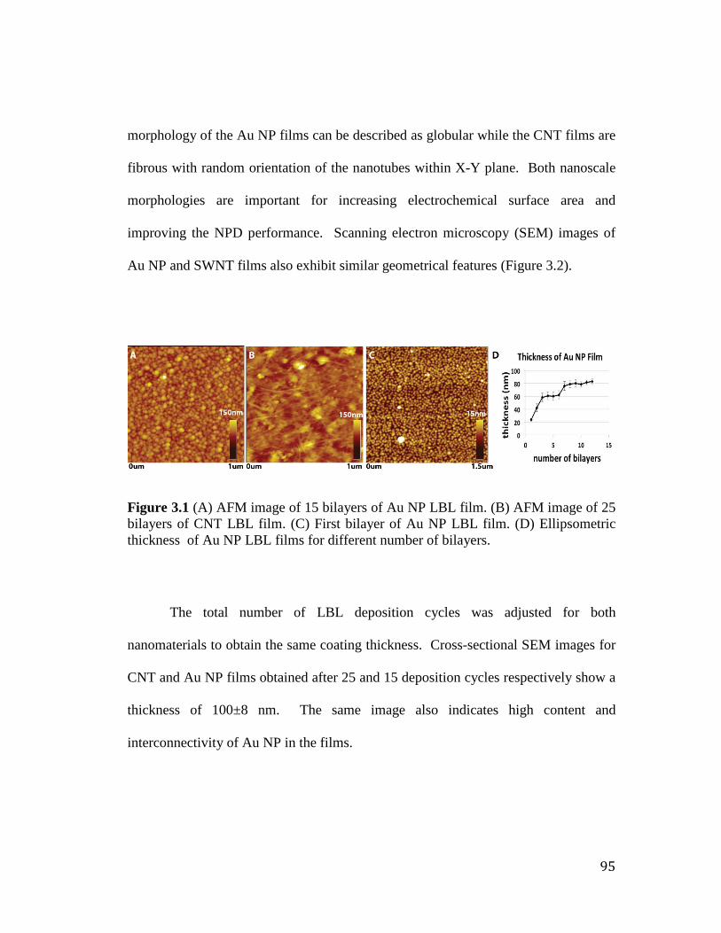
95
morphology of the Au NP films can be described as globular while the CNT films are
fibrous with random orientation of the nanotubes within X-Y plane. Both nanoscale
morphologies are important for increasing electrochemical surface area and
improving the NPD performance. Scanning electron microscopy (SEM) images of
Au NP and SWNT films also exhibit similar geometrical features (Figure 3.2).
Figure 3.1 (A) AFM image of 15 bilayers of Au NP LBL film. (B) AFM image of 25 bilayers of CNT LBL film. (C) First bilayer of Au NP LBL film. (D) Ellipsometric thickness of Au NP LBL films for different number of bilayers.
The total number of LBL deposition cycles was adjusted for both
nanomaterials to obtain the same coating thickness. Cross-sectional SEM images for
CNT and Au NP films obtained after 25 and 15 deposition cycles respectively show a
thickness of 100±8 nm. The same image also indicates high content and
interconnectivity of Au NP in the films.
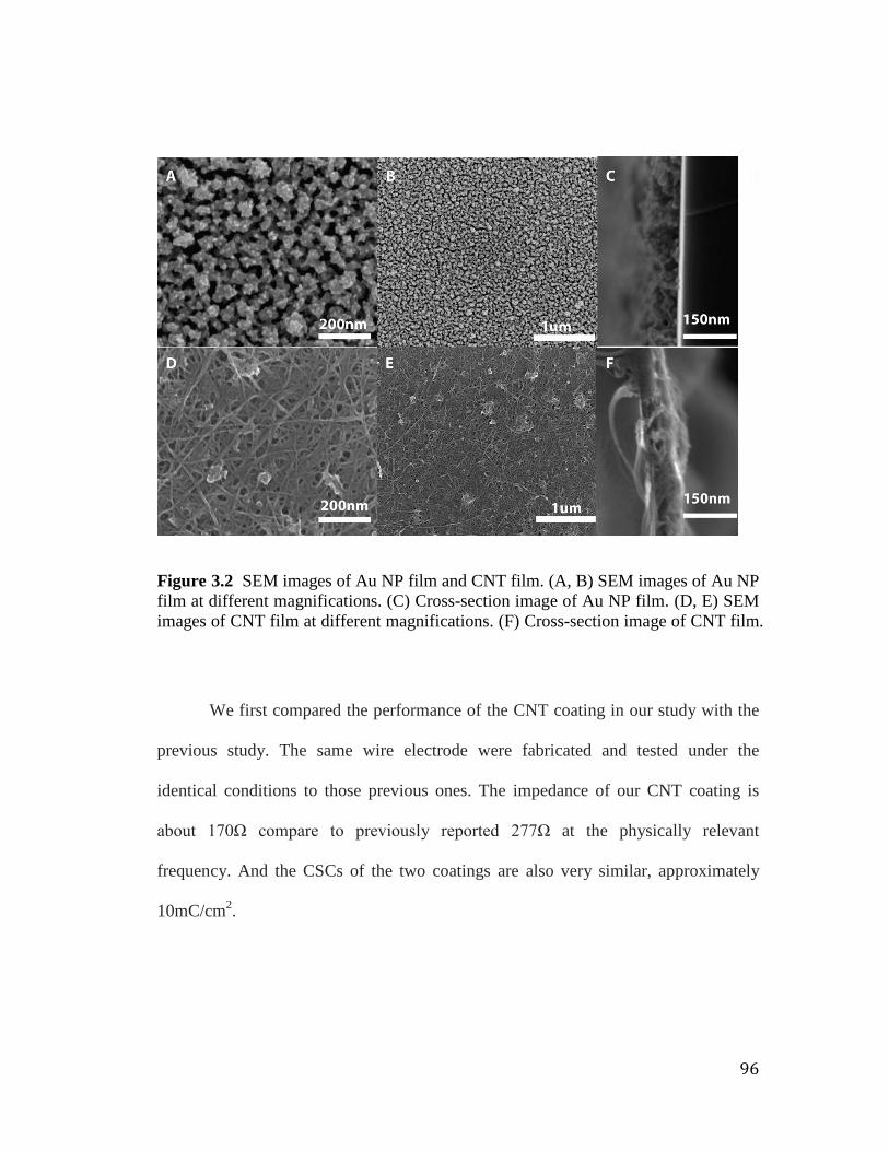
96
Figure 3.2 SEM images of Au NP film and CNT film. (A, B) SEM images of Au NP film at different magnifications. (C) Cross-section image of Au NP film. (D, E) SEM images of CNT film at different magnifications. (F) Cross-section image of CNT film.
We first compared the performance of the CNT coating in our study with the
previous study. The same wire electrode were fabricated and tested under the
identical conditions to those previous ones. The impedance of our CNT coating is
about 170Ω compare to previously reported 277Ω at the physically relevant
frequency. And the CSCs of the two coatings are also very similar, approximately
10mC/cm2.
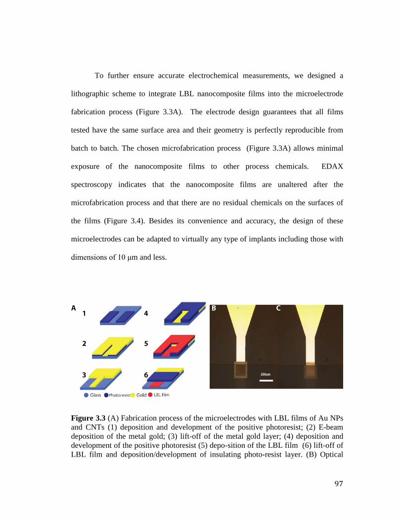
97
To further ensure accurate electrochemical measurements, we designed a
lithographic scheme to integrate LBL nanocomposite films into the microelectrode
fabrication process (Figure 3.3A). The electrode design guarantees that all films
tested have the same surface area and their geometry is perfectly reproducible from
batch to batch. The chosen microfabrication process (Figure 3.3A) allows minimal
exposure of the nanocomposite films to other process chemicals. EDAX
spectroscopy indicates that the nanocomposite films are unaltered after the
microfabrication process and that there are no residual chemicals on the surfaces of
the films (Figure 3.4). Besides its convenience and accuracy, the design of these
microelectrodes can be adapted to virtually any type of implants including those with
dimensions of 10 μm and less.
Figure 3.3 (A) Fabrication process of the microelectrodes with LBL films of Au NPs and CNTs (1) deposition and development of the positive photoresist; (2) E-beam deposition of the metal gold; (3) lift-off of the metal gold layer; (4) deposition and development of the positive photoresist (5) depo-sition of the LBL film (6) lift-off of LBL film and deposition/development of insulating photo-resist layer. (B) Optical
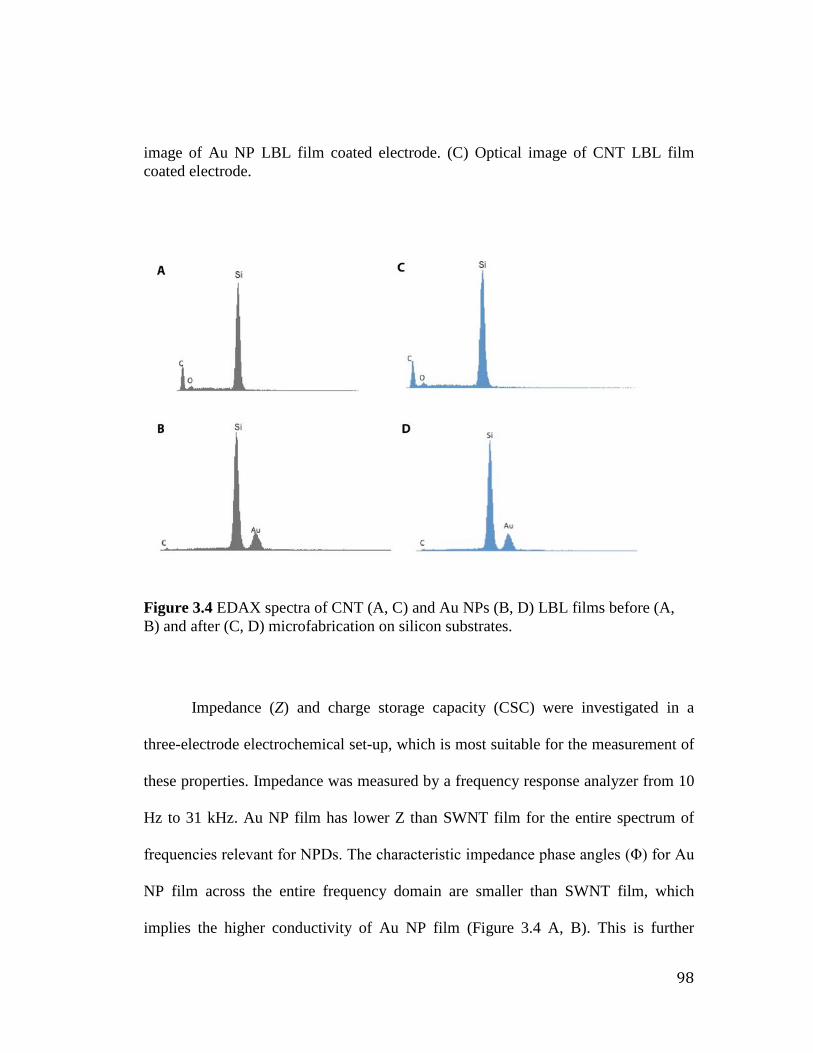
98
image of Au NP LBL film coated electrode. (C) Optical image of CNT LBL film coated electrode.
Figure 3.4 EDAX spectra of CNT (A, C) and Au NPs (B, D) LBL films before (A, B) and after (C, D) microfabrication on silicon substrates.
Impedance (Z) and charge storage capacity (CSC) were investigated in a
three-electrode electrochemical set-up, which is most suitable for the measurement of
these properties. Impedance was measured by a frequency response analyzer from 10
Hz to 31 kHz. Au NP film has lower Z than SWNT film for the entire spectrum of
frequencies relevant for NPDs. The characteristic impedance phase angles (Φ) for Au
NP film across the entire frequency domain are smaller than SWNT film, which
implies the higher conductivity of Au NP film (Figure 3.4 A, B). This is further
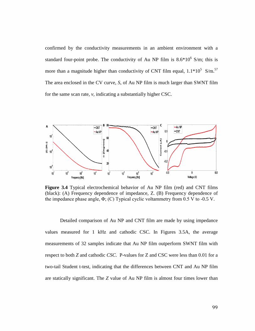
99
confirmed by the conductivity measurements in an ambient environment with a
standard four-point probe. The conductivity of Au NP film is 8.6*106 S/m; this is
more than a magnitude higher than conductivity of CNT film equal, 1.1*105 S/m.57
The area enclosed in the CV curve, S, of Au NP film is much larger than SWNT film
for the same scan rate, v, indicating a substantially higher CSC.
Figure 3.4 Typical electrochemical behavior of Au NP film (red) and CNT films (black): (A) Frequency dependence of impedance, Z. (B) Frequency dependence of the impedance phase angle, Φ; (C) Typical cyclic voltammetry from 0.5 V to -0.5 V.
Detailed comparison of Au NP and CNT film are made by using impedance
values measured for 1 kHz and cathodic CSC. In Figures 3.5A, the average
measurements of 32 samples indicate that Au NP film outperform SWNT film with
respect to both Z and cathodic CSC. P-values for Z and CSC were less than 0.01 for a
two-tail Student t-test, indicating that the differences between CNT and Au NP film
are statically significant. The Z value of Au NP film is almost four times lower than
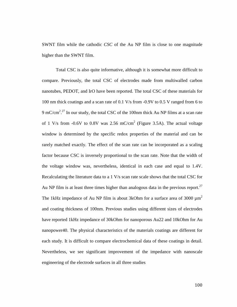
100
SWNT film while the cathodic CSC of the Au NP film is close to one magnitude
higher than the SWNT film.
Total CSC is also quite informative, although it is somewhat more difficult to
compare. Previously, the total CSC of electrodes made from multiwalled carbon
nanotubes, PEDOT, and IrO have been reported. The total CSC of these materials for
100 nm thick coatings and a scan rate of 0.1 V/s from -0.9V to 0.5 V ranged from 6 to
9 mC/cm2.27 In our study, the total CSC of the 100nm thick Au NP films at a scan rate
of 1 V/s from -0.6V to 0.8V was 2.56 mC/cm2 (Figure 3.5A). The actual voltage
window is determined by the specific redox properties of the material and can be
rarely matched exactly. The effect of the scan rate can be incorporated as a scaling
factor because CSC is inversely proportional to the scan rate. Note that the width of
the voltage window was, nevertheless, identical in each case and equal to 1.4V.
Recalculating the literature data to a 1 V/s scan rate scale shows that the total CSC for
Au NP film is at least three times higher than analogous data in the previous report.27
The 1kHz impedance of Au NP film is about 3kOhm for a surface area of 3000 µm2
and coating thickness of 100nm. Previous studies using different sizes of electrodes
have reported 1kHz impedance of 30kOhm for nanoporous Au22 and 10kOhm for Au
nanopower40. The physical characteristics of the materials coatings are different for
each study. It is difficult to compare electrochemical data of these coatings in detail.
Nevertheless, we see significant improvement of the impedance with nanoscale
engineering of the electrode surfaces in all three studies
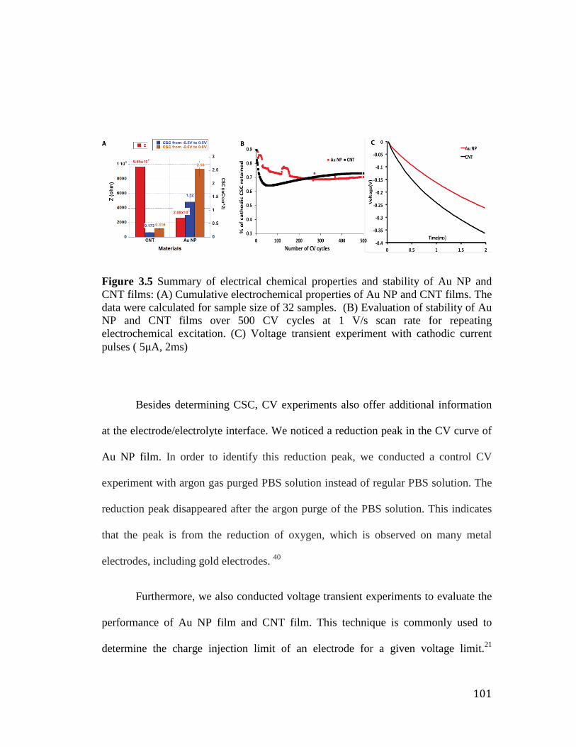
101
Figure 3.5 Summary of electrical chemical properties and stability of Au NP and CNT films: (A) Cumulative electrochemical properties of Au NP and CNT films. The data were calculated for sample size of 32 samples. (B) Evaluation of stability of Au NP and CNT films over 500 CV cycles at 1 V/s scan rate for repeating electrochemical excitation. (C) Voltage transient experiment with cathodic current pulses ( 5µA, 2ms)
Besides determining CSC, CV experiments also offer additional information
at the electrode/electrolyte interface. We noticed a reduction peak in the CV curve of
Au NP film. In order to identify this reduction peak, we conducted a control CV
experiment with argon gas purged PBS solution instead of regular PBS solution. The
reduction peak disappeared after the argon purge of the PBS solution. This indicates
that the peak is from the reduction of oxygen, which is observed on many metal
electrodes, including gold electrodes. 40
Furthermore, we also conducted voltage transient experiments to evaluate the
performance of Au NP film and CNT film. This technique is commonly used to
determine the charge injection limit of an electrode for a given voltage limit.21
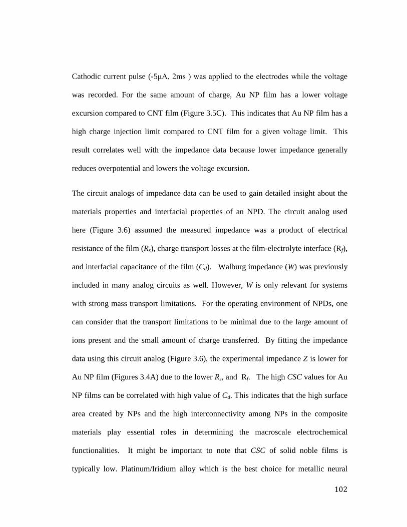
102
Cathodic current pulse (-5μA, 2ms ) was applied to the electrodes while the voltage
was recorded. For the same amount of charge, Au NP film has a lower voltage
excursion compared to CNT film (Figure 3.5C). This indicates that Au NP film has a
high charge injection limit compared to CNT film for a given voltage limit. This
result correlates well with the impedance data because lower impedance generally
reduces overpotential and lowers the voltage excursion.
The circuit analogs of impedance data can be used to gain detailed insight about the
materials properties and interfacial properties of an NPD. The circuit analog used
here (Figure 3.6) assumed the measured impedance was a product of electrical
resistance of the film (Rs), charge transport losses at the film-electrolyte interface (Rf),
and interfacial capacitance of the film (Cd). Walburg impedance (W) was previously
included in many analog circuits as well. However, W is only relevant for systems
with strong mass transport limitations. For the operating environment of NPDs, one
can consider that the transport limitations to be minimal due to the large amount of
ions present and the small amount of charge transferred. By fitting the impedance
data using this circuit analog (Figure 3.6), the experimental impedance Z is lower for
Au NP film (Figures 3.4A) due to the lower Rs, and Rf. The high CSC values for Au
NP films can be correlated with high value of Cd. This indicates that the high surface
area created by NPs and the high interconnectivity among NPs in the composite
materials play essential roles in determining the macroscale electrochemical
functionalities. It might be important to note that CSC of solid noble films is
typically low. Platinum/Iridium alloy which is the best choice for metallic neural
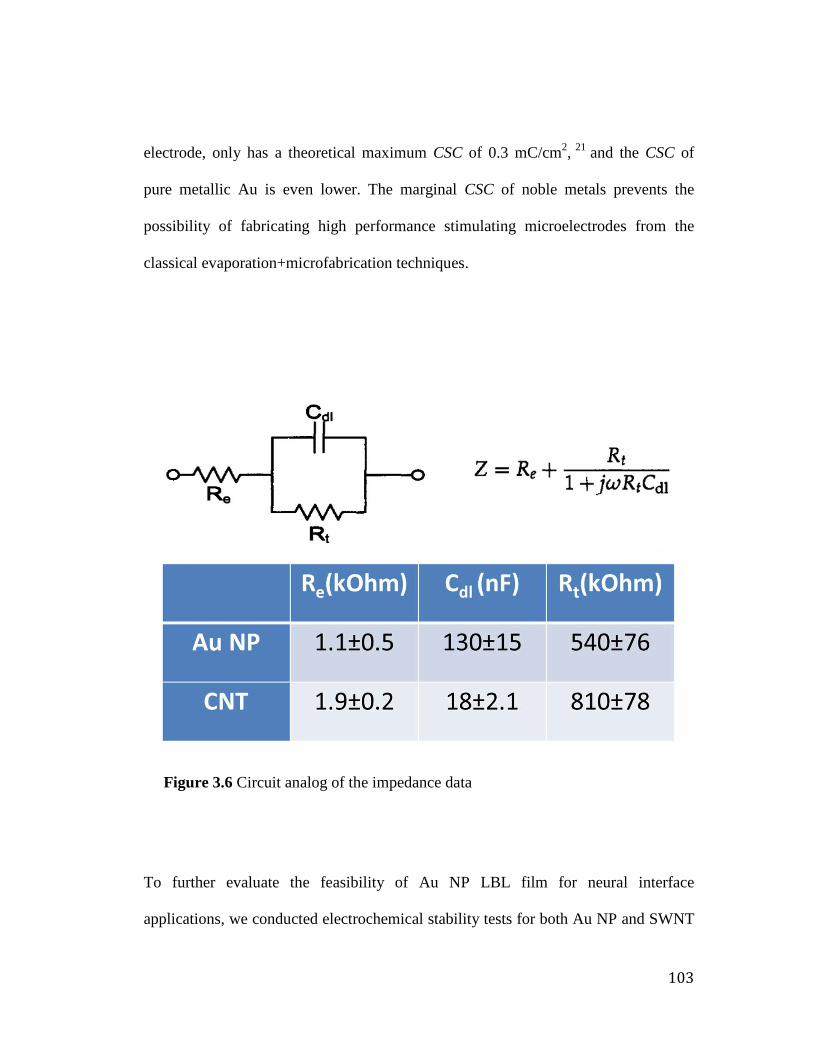
103
electrode, only has a theoretical maximum CSC of 0.3 mC/cm2, 21 and the CSC of
pure metallic Au is even lower. The marginal CSC of noble metals prevents the
possibility of fabricating high performance stimulating microelectrodes from the
classical evaporation+microfabrication techniques.
Figure 3.6 Circuit analog of the impedance data
To further evaluate the feasibility of Au NP LBL film for neural interface
applications, we conducted electrochemical stability tests for both Au NP and SWNT
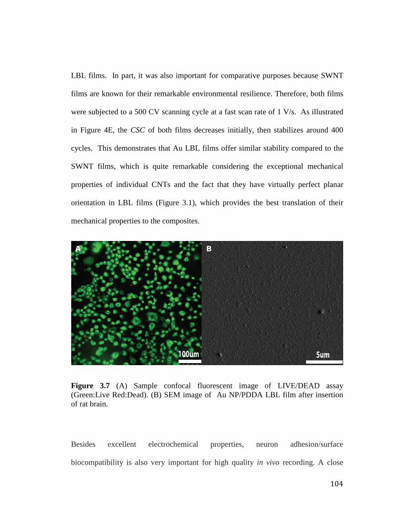
104
LBL films. In part, it was also important for comparative purposes because SWNT
films are known for their remarkable environmental resilience. Therefore, both films
were subjected to a 500 CV scanning cycle at a fast scan rate of 1 V/s. As illustrated
in Figure 4E, the CSC of both films decreases initially, then stabilizes around 400
cycles. This demonstrates that Au LBL films offer similar stability compared to the
SWNT films, which is quite remarkable considering the exceptional mechanical
properties of individual CNTs and the fact that they have virtually perfect planar
orientation in LBL films (Figure 3.1), which provides the best translation of their
mechanical properties to the composites.
Figure 3.7 (A) Sample confocal fluorescent image of LIVE/DEAD assay (Green:Live Red:Dead). (B) SEM image of Au NP/PDDA LBL film after insertion of rat brain.
Besides excellent electrochemical properties, neuron adhesion/surface
biocompatibility is also very important for high quality in vivo recording. A close
105
interface between electrode/neuron improves the quality of the recording.14, 20 The
biocompatibility of the Au NP/PDDA coating was tested with in-vitro culture of
NG108-15 cells, a type of mouse neuroblastoma/glioma hybrid cells, which are
typically used in many biocompatibility/toxicity protocols58. Cells were seeded and
cultured on glass slides coated with Au NP/PDDA film. Optical images showed
NG108 cells could adhere well on the coating and differentiate into neuron-like
morphology. (See Supplemental Information) Live/Dead assay were also performed
and indicated that 99.9% of cells were live on the surface of the Au NP/PDDA
coating (Figure 3.7A). Additionally, the mechanical integrity of Au NP film was also
examined by an ex-vivo insertion test. The electrodes coated with Au NP/PDDA were
inserted into a fresh harvested rat brain and kept at 4°C for 3 days. Then the
electrodes were removed from the brain, rinsed with PBS, and imaged with SEM. The
Au NP/PDDA coating surface retains the same nanoscale roughness as observed
before the insertion (Figure 3.5B).
2.4 Conclusion
Quite unexpectedly, Au NP films were found to have remarkable charge
transfer capacity, substantially lower impedance and comparable electrochemical
stability under fast voltage scans than CNT films made using the same technology,
which were previously considered to be the most promising new materials for the
next generation of implantable neuroprosthetic devices (NPDs). Besides the
106
electrochemical performance, we also see additional advantages of the described Au
NP films with respect to other (nano)materials: (1) the long-standing clinical record
of gold in both nano- and macroscale forms will facilitate their acceptance; (2) LBL
assembly offers tremendous possibilities for further optimization and adaptation to
additional NPD functions, which for instance can include in-situ gene delivery.59
Further improvement of materials performance is also possible using LBL films from
novel Au NPs, such as nanoshells and nanostars.
A general microfabrication process for Au NP LBL composites suitable for
preparation of ultrasmall implantable electrodes that can be virtually “invisible” to the
immune system was designed and realized. Integration of LBL film deposition
technology and traditional lithography opens many possibilities for utilization of
nanostructured LBL composites from CNTs, NPs, etc and their unique properties in
many applications.
Further optimization at the system level combining the material properties of
Au NP composites and microfabrication techniques must also be pursued. Fabrication
of electrodes, which are mechanically compliant with the soft neural tissues and in
vivo evaluation of this type of microelectrodes, should be the next logical step in this
field. A flexible and high performance electrode made out of Au NP film could
minimize the tissue stress and provide long-term stability for future neural prosthetic
devices.
107
2.5 References
1. Callaghan, J. C.; Bigelow, W. G., An Electrical Artificial Pacemaker for
Standstill of the Heart. Ann Surg 1951, 134, 8-17.
2. Fallon, J. B.; Irvine, D. R.; Shepherd, R. K., Cochlear Implants and Brain
Plasticity. Hear Res 2008, 238, 110-7.
3. Pena, C.; Bowsher, K.; Samuels-Reid, J., Fda-Approved Neurologic Devices
Intended for Use in Infants, Children, and Adolescents. Neurology 2004, 63, 1163-
1167.
4. Hamani, C.; McAndrews, M. P.; Cohn, M.; Oh, M.; Zumsteg, D.; Shapiro, C.
M.; Wennberg, R. A.; Lozano, A. M., Memory Enhancement Induced by
Hypothalamic/Fornix Deep Brain Stimulation. Ann Neurol 2008, 63, 119-23.
5. Nijboer, F.; Sellers, E. W.; Mellinger, J.; Jordan, M. A.; Matuz, T.; Furdea,
A.; Halder, S.; Mochty, U.; Krusienski, D. J.; Vaughan, T. M.; Wolpaw, J. R.;
Birbaumer, N.; Kubler, A., A P300-Based Brain-Computer Interface for People with
Amyotrophic Lateral Sclerosis. Clinical neurophysiology : official journal of the
International Federation of Clinical Neurophysiology 2008, 119, 1909-16.
6. Velliste, M.; Perel, S.; Spalding, M. C.; Whitford, A. S.; Schwartz, A. B.,
Cortical Control of a Prosthetic Arm for Self-Feeding. Nature 2008, 453, 1098-101.
7. Moritz, C. T.; Perlmutter, S. I.; Fetz, E. E., Direct Control of Paralysed
Muscles by Cortical Neurons. Nature 2008, 456, 639-42.
108
8. Biran, R.; Martin, D. C.; Tresco, P. A., Neuronal Cell Loss Accompanies the
Brain Tissue Response to Chronically Implanted Silicon Microelectrode Arrays. Exp
Neurol 2005, 195, 115-26.
9. Edell, D. J.; Toi, V. V.; McNeil, V. M.; Clark, L. D., Factors Influencing the
Biocompatibility of Insertable Silicon Microshafts in Cerebral Cortex. IEEE Trans
Biomed Eng 1992, 39, 635-43.
10. Davies, S. J.; Fitch, M. T.; Memberg, S. P.; Hall, A. K.; Raisman, G.; Silver,
J., Regeneration of Adult Axons in White Matter Tracts of the Central Nervous
System. Nature 1997, 390, 680-3.
11. Kim, Y. T.; Hitchcock, R. W.; Bridge, M. J.; Tresco, P. A., Chronic Response
of Adult Rat Brain Tissue to Implants Anchored to the Skull. Biomaterials 2004, 25,
2229-37.
12. Keohan, F.; Wei, X. F.; Wongsarnpigoon, A.; Lazaro, E.; Darga, J. E.; Grill,
W. M., Fabrication and Evaluation of Conductive Elastomer Electrodes for Neural
Stimulation. J Biomater Sci Polym Ed 2007, 18, 1057-73.
13. Sanders, J. E.; Stiles, C. E.; Hayes, C. L., Tissue Response to Single-Polymer
Fibers of Varying Diameters: Evaluation of Fibrous Encapsulation and Macrophage
Density. J Biomed Mater Res 2000, 52, 231-7.
14. Hai, A.; Shappir, J.; Spira, M. E., In-Cell Recordings by Extracellular
Microelectrodes. Nat Methods 2010, 7, 200-2.

109
15. Subbaroyan, J.; Martin, D. C.; Kipke, D. R., A Finite-Element Model of the
Mechanical Effects of Implantable Microelectrodes in the Cerebral Cortex. J Neural
Eng 2005, 2, 103-13.
16. Seymour, J. P.; Kipke, D. R., Neural Probe Design for Reduced Tissue
Encapsulation in Cns. Biomaterials 2007, 28, 3594-607.
17. Gilletti, A.; Muthuswamy, J., Brain Micromotion around Implants in the
Rodent Somatosensory Cortex. J Neural Eng 2006, 3, 189-95.
18. Merrill, D. R.; Bikson, M.; Jefferys, J. G., Electrical Stimulation of Excitable
Tissue: Design of Efficacious and Safe Protocols. J Neurosci Methods 2005, 141,
171-98.
19. Harnack, D.; Winter, C.; Meissner, W.; Reum, T.; Kupsch, A.; Morgenstern,
R., The Effects of Electrode Material, Charge Density and Stimulation Duration on
the Safety of High-Frequency Stimulation of the Subthalamic Nucleus in Rats. J
Neurosci Methods 2004, 138, 207-16.
20. Keefer, E. W.; Botterman, B. R.; Romero, M. I.; Rossi, A. F.; Gross, G. W.,
Carbon Nanotube Coating Improves Neuronal Recordings. Nat Nanotechnol 2008, 3,
434-9.
21. Cogan, S. F., Neural Stimulation and Recording Electrodes. Annu Rev Biomed
Eng 2008, 10, 275-309.
22. Seker, E.; Berdichevsky, Y.; Begley, M. R.; Reed, M. L.; Staley, K. J.;
Yarmush, M. L., The Fabrication of Low-Impedance Nanoporous Gold Multiple-
110
Electrode Arrays for Neural Electrophysiology Studies. Nanotechnology 2010, 21,
125504.
23. Marrese, C. A., Preparation of Strongly Adherent Platinum Black Coatings.
Anal Chem 1987, 59, 217-218.
24. Richardson-Burns, S. M.; Hendricks, J. L.; Foster, B.; Povlich, L. K.; Kim, D.
H.; Martin, D. C., Polymerization of the Conducting Polymer Poly(3,4-
Ethylenedioxythiophene) (Pedot) around Living Neural Cells. Biomaterials 2007, 28,
1539-52.
25. Blau, A.; Ziegler, C.; Heyer, M.; Endres, F.; Schwitzgebel, G.; Matthies, T.;
Stieglitz, T.; Meyer, J. U.; Gopel, W., Characterization and Optimization of
Microelectrode Arrays for in Vivo Nerve Signal Recording and Stimulation. Biosens
Bioelectron 1997, 12, 883-92.
26. Jan, E.; Hendricks, J. L.; Husaini, V.; Richardson-Burns, S. M.; Sereno, A.;
Martin, D. C.; Kotov, N. A., Layered Carbon Nanotube-Polyelectrolyte Electrodes
Outperform Traditional Neural Interface Materials. Nano Letters 2009, 9, 4012-4018.
27. Jan, E.; Kotov, N. A., Successful Differentiation of Mouse Neural Stem Cells
on Layer-by-Layer Assembled Single-Walled Carbon Nanotube Composite. Nano
Letters 2007, 7, 1123-1128.
28. Kam, N. W. S.; Jan, E.; Kotov, N. A., Electrical Stimulation of Neural Stem
Cells Mediated by Humanized Carbon Nanotube Composite Made with Extracellular
Matrix Protein. Nano Letters 2009, 9, 273-278.

111
29. Gheith, M. K.; Sinani, V. A.; Wicksted, J. P.; Matts, R. L.; Kotov, N. A.,
Single-Walled Carbon Nanotube Polyelectrolyte Multilayers and Freestanding Films
as a Biocompatible Platformfor Neuroprosthetic Implants. Advanced Materials 2005,
17, 2663-+.
30. Luo, X.; Weaver, C. L.; Zhou, D. D.; Greenberg, R.; Cui, X. T., Highly Stable
Carbon Nanotube Doped Poly(3,4-Ethylenedioxythiophene) for Chronic Neural
Stimulation. Biomaterials 2011, 32, 5551-7.
31. Lovat, V.; Pantarotto, D.; Lagostena, L.; Cacciari, B.; Grandolfo, M.; Righi,
M.; Spalluto, G.; Prato, M.; Ballerini, L., Carbon Nanotube Substrates Boost
Neuronal Electrical Signaling. Nano Letters 2005, 5, 1107-1110.
32. Malarkey, E. B.; Fisher, K. A.; Bekyarova, E.; Liu, W.; Haddon, R. C.;
Parpura, V., Conductive Single-Walled Carbon Nanotube Substrates Modulate
Neuronal Growth. Nano Letters 2009, 9, 264-268.
33. Cellot, G.; Cilia, E.; Cipollone, S.; Rancic, V.; Sucapane, A.; Giordani, S.;
Gambazzi, L.; Markram, H.; Grandolfo, M.; Scaini, D.; Gelain, F.; Casalis, L.; Prato,
M.; Giugliano, M.; Ballerini, L., Carbon Nanotubes Might Improve Neuronal
Performance by Favouring Electrical Shortcuts. Nat Nanotechnol 2009, 4, 126-133.
34. Malarkey, E. B.; Parpura, V., Carbon Nanotubes in Neuroscience. Act Neur S
2010, 106, 337-341.
35. Luo, X. L.; Weaver, C. L.; Zhou, D. D.; Greenberg, R.; Cui, X. Y. T., Highly
Stable Carbon Nanotube Doped Poly(3,4-Ethylenedioxythiophene) for Chronic
Neural Stimulation. Biomaterials 2011, 32, 5551-5557.
112
36. Wang, K.; Fishman, H. A.; Dai, H. J.; Harris, J. S., Neural Stimulation with a
Carbon Nanotube Microelectrode Array. Nano Letters 2006, 6, 2043-2048.
37. Firme, C. P., 3rd; Bandaru, P. R., Toxicity Issues in the Application of Carbon
Nanotubes to Biological Systems. Nanomedicine 2010, 6, 245-56.
38. Cohen-Karni, T.; Qing, Q.; Li, Q.; Fang, Y.; Lieber, C. M., Graphene and
Nanowire Transistors for Cellular Interfaces and Electrical Recording. Nano Letters
2010, 10, 1098-1102.
39. Qing, Q.; Pal, S. K.; Tian, B. Z.; Duan, X. J.; Timko, B. P.; Cohen-Karni, T.;
Murthy, V. N.; Lieber, C. M., Nanowire Transistor Arrays for Mapping Neural
Circuits in Acute Brain Slices. P Natl Acad Sci USA 2010, 107, 1882-1887.
40. Hu, Z.; Zhou, D. M.; Greenberg, R.; Thundat, T., Nanopowder Molding
Method for Creating Implantable High-Aspect-Ratio Electrodes on Thin Flexible
Substrates. Biomaterials 2006, 27, 2009-17.
41. Sperling, R. A.; Rivera Gil, P.; Zhang, F.; Zanella, M.; Parak, W. J.,
Biological Applications of Gold Nanoparticles. Chem Soc Rev 2008, 37, 1896-908.
42. Zhang, X. D.; Wu, H. Y.; Wu, D.; Wang, Y. Y.; Chang, J. H.; Zhai, Z. B.;
Meng, A. M.; Liu, P. X.; Zhang, L. A.; Fan, F. Y., Toxicologic Effects of Gold
Nanoparticles in Vivo by Different Administration Routes. Int J Nanomedicine 2010,
5, 771-81.
43. Critchley, K.; Khanal, B. P.; Gorzny, M. L.; Vigderman, L.; Evans, S. D.;
Zubarev, E. R.; Kotov, N. A., Near-Bulk Conductivity of Gold Nanowires as
113
Nanoscale Interconnects and the Role of Atomically Smooth Interface. Advanced
Materials 2010, 22, 2338-42.
44. Turkevich, J.; Stevenson, P. C.; Hillier, J., A Study of the Nucleation and
Growth Processes in the Synthesis of Colloidal Gold. Discuss Faraday Soc 1951, 55-
&.
45. Liu, Y. J.; Wang, Y. X.; Claus, R. O., Layer-by-Layer Ionic Self-Assembly of
Au Colloids into Multilayer Thin-Films with Bulk Metal Conductivity. Chemical
Physics Letters 1998, 298, 315-319.
46. Shim, B. S.; Zhu, J.; Jan, E.; Critchley, K.; Ho, S. S.; Podsiadlo, P.; Sun, K.;
Kotov, N. A., Multiparameter Structural Optimization of Single-Walled Carbon
Nanotube Composites: Toward Record Strength, Stiffness, and Toughness. Acs Nano
2009, 3, 1711-1722.
47. Odintsov, A. A., Schottky Barriers in Carbon Nanotube Heterojunctions. Phys
Rev Lett 2000, 85, 150-153.
48. Kagan, V. E.; Konduru, N. V.; Feng, W. H.; Allen, B. L.; Conroy, J.; Volkov,
Y.; Vlasova, I. I.; Belikova, N. A.; Yanamala, N.; Kapralov, A.; Tyurina, Y. Y.; Shi, J.
W.; Kisin, E. R.; Murray, A. R.; Franks, J.; Stolz, D.; Gou, P. P.; Klein-Seetharaman,
J.; Fadeel, B.; Star, A.; Shvedova, A. A., Carbon Nanotubes Degraded by Neutrophil
Myeloperoxidase Induce Less Pulmonary Inflammation. Nat Nanotechnol 2010, 5,
354-359.
114
49. Thakor, A. S.; Jokerst, J.; Zavaleta, C.; Massoud, T. F.; Gambhir, S. S., Gold
Nanoparticles: A Revival in Precious Metal Administration to Patients. Nano Letters
2011, 11, 4029-4036.
50. Kotov, N. A.; Winter, J. O.; Clements, I. P.; Jan, E.; Timko, B. P.; Campidelli,
S.; Pathak, S.; Mazzatenta, A.; Lieber, C. M.; Prato, M.; Bellamkonda, R. V.; Silva, G.
A.; Kam, N. W. S.; Patolsky, F.; Ballerini, L., Nanomaterials for Neural Interfaces.
Advanced Materials 2009, 21, 3970-4004.
51. Srivastava, S.; Kotov, N. A., Composite Layer-by-Layer (Lbl) Assembly with
Inorganic Nanoparticles and Nanowires. Acc Chem Res 2008, 41, 1831-41.
52. Shim, B. S.; Zhu, J.; Jan, E.; Critchley, K.; Ho, S.; Podsiadlo, P.; Sun, K.;
Kotov, N. A., Multiparameter Structural Optimization of Single-Walled Carbon
Nanotube Composites: Toward Record Strength, Stiffness, and Toughness. Acs Nano
2009, 3, 1711-22.
53. Zhu, J.; Shim, B. S.; Di Prima, M.; Kotov, N. A., Transparent Conductors
from Carbon Nanotubes Lbl-Assembled with Polymer Dopant with Pi-Pi Electron
Transfer. J Am Chem Soc 2011, 133, 7450-60.
54. Shim, B. S.; Zhu, J.; Jan, E.; Critchley, K.; Kotov, N. A., Transparent
Conductors from Layer-by-Layer Assembled Swnt Films: Importance of Mechanical
Properties and a New Figure of Merit. Acs Nano 2010, 4, 3725-34.
55. Shim, B. S.; Tang, Z. Y.; Morabito, M. P.; Agarwal, A.; Hong, H. P.; Kotov,
N. A., Integration of Conductivity Transparency, and Mechanical Strength into
115
Highly Homogeneous Layer-by-Layer Composites of Single-Walled Carbon
Nanotubes for Optoelectronics. Chemistry of Materials 2007, 19, 5467-5474.
56. Sinani, V. A.; Koktysh, D. S.; Yun, B. G.; Matts, R. L.; Pappas, T. C.;
Motamedi, M.; Thomas, S. N.; Kotov, N. A., Collagen Coating Promotes
Biocompatibility of Semiconductor Nanoparticles in Stratified Lbl Films. Nano
Letters 2003, 3, 1177-1182.
57. Zhu, J.; Shim, B. S.; Di Prima, M.; Kotov, N. A., Transparent Conductors
from Carbon Nanotubes Lbl-Assembled with Polymer Dopant with Pi-Pi Electron
Transfer. J Am Chem Soc 2011, 133, 7450-7460.
58. Adler, M.; Shafer, H.; Hamilton, T.; Petrali, J. P., Cytotoxic Actions of the
Heavy Metal Chelator Tpen on Ng108-15 Neuroblastoma-Glioma Cells.
Neurotoxicology 1999, 20, 571-82.
59. Jan, E.; Pereira, F. N.; Turner, D. L.; Kotov, N. A., In Situ Gene Transfection
and Neuronal Programming on Electroconductive Nanocomposite to Reduce
Inflammatory Response. Journal of Materials Chemistry 2011, 21, 1109-1114.

116
Chapter 4
Aramid Nanofiber and Epoxy Composite as Multifunctional Insulation Material
for Implantable Electronics
4.1 Abstract
Insulation materials are vital for the functionality and biocompatibility of the
implantable electronics. Delamination of insulation materials leads to device failure.
Ideally, insulation material should be chemically inert, biocompatible, and has great
adhesion etc. However, many materials currently developed has limited performance
in term of these desirable properties. We successfully create a nanocomposite
material by combining aramid nanofiber, epoxy resin, and polyethylene glycol. The
final nanocomposite demonstrates superior adhesion, biocompatibility, and
antifouling property, compared to parylene C. This study opens doors to a new
nanocomposite approach to design insulation materials for implantable electronics.
117
4.2 Introduction
Implantable microelectronic devices are crucial for advancing diagnostics and
therapy of many medical conditions.1 Cochlear implant,2, 3 deep brain stimulation
electrodes,4 implantable neural recording devices5, 6 exemplify some of the major
achievements in this area. Recent studies on implantable electronics reveal that
mechanically flexible devices might have many advantages in term of
biocompatibility.7 Therefore, much research has been devoted to create electronic
circuits on flexible polymer substrates. 8-12 Advances in microfabrication technology
allow us to create high density electrical components for development of the
ultrasmall and multifunctional implantable electronic devices on flexible substrate.
High density and ultrasmall electrode arrays have the advantage of targeting
specific tissue regions, covering larger spatial area, and acquiring high signal to noise
ratio data.13 Insulation material is the key component to achieve these desirable
functionalities of the high density electrode arrays. First of all, in the multi-electrode
array configuration, it is necessary to have each electrode function independently.
Insulation materials are commonly applied to separation each electrodes and prevent
“cross talk” from neighboring electrodes.14 As such, the adhesion properties of the
insulation materials are very important. Additionally, the electrical components of
these implantable systems require isolation from the biological fluids. Otherwise, the
contact of the biological fluid with electrical component would create short circuit or
erode the electrical component.15 Insulation materials serve as a barrier to protect the
118
electronic circuits. The insulation materials are utilized to define the specific
functional sites of the electrical components that interact with surrounding tissue. The
amount of the electrically active surface area in contact with the surround tissue is
also crucial to the functionality of the devices. In this case, delamination of insulation
materials inevitably induces other device failure modes.16 Thus, it is important to
develop reliable adhesion materials for insulation.
Insulation materials for implantable electronics also have close interaction
with the surrounding tissue. Therefore, the surface properties and bioactivity of the
insulation materials are key factors for tissue response and the functionality of
implantable devices, in addition to the adhesion properties. For instance, anti-fouling
surfaces with polyethylene glycol on biomedical devices are known for reducing the
interaction between the device and biological fluid.17 This reduction of protein
absorption on the devices surface improves device acceptance by biological tissues.
Drug releasing coatings on bare metal and artificial hips have been well developed
and commercialized in the clinical setting to improve the long term functionality and
biocompatibility of the devices.18-20 Studies on brain implants also demonstrated that
anti-inflammation coating and adhesion protein coating also improve the
biocompatibility of the devices. 21, 22 Therefore, it is advantageous to have ability to
modulate the surface properties of the insulation coating.
To summarize, there are several material requirements for an ideal flexible
insulation material: a) electrical insulation to prevent electron transfer and short
119
circuiting, b) strong metal adhesion to protect the metal component under
physiological condition c) strong interfacial adhesion between layers to avoid
delamination, d) excellent biocompatibility for chronic applications e) excellent
barrier for ion, water, and oxygen, and f) compatible with microfabrication process.
Parylene C has been widely adopted as an insulation material for implantable
electronics. It is deposited through the chemical vapor deposition method (CVD).
The final product is uniform and pinhole free, which is ideal for the microfabrication
process. Additionally, parylene C is chemically inert and has high electrical
resistivity.23 Advances in parylene synthesis also developed parylene with additional
functional group. This allows further functionalization of the parylene surface, which
is very attractive for biomedical applications.16, 24 Nevertheless, due to the
hydrophobic nature of parylene C, it has known complications with adhesion on
metal and interfacial adhesion, which causes chronic device failure.25-27 Several
different approaches have been developed to improve the adhesion of the parylene C.
High temperature and pressure treatment has been approved as an effective method to
improve the adhesion of parylene C.28 However, this method requires high
temperature and pressure conditions, which could have adverse effect on the other
components of the devices. Alternatively, researchers also developed parylene with
additional function groups for further crosslinking and improving interfacial
adhesion.16 Nevertheless, parylene with additional functional groups is not readily
available commercially yet. Many polymeric materials are also considered as an
insulating layer, including Telfon,29 epoxy resin,30 and polyimide.31 However, there
120
are very limit studies related to systematic evaluation of the adhesion performance of
these materials.
Recent developments in aramid nanofiber dispersion offer a new framework
to design composite materials with tailored functionalities.32, 33 By dissolution of
aramid bulk fibers in solvents, aramid nanofibers in dimethyl sulfoxide (DMSO) can
be controlled from 3 nm to 30nm in diameter.32 The uniform dispersion of the
nanofibers in solution and the branched structures of the nanofibers allow us to create
uniform and highly porous film via spin coating. Moreover, the uniform and porous
film from ANF can serve a platform for other material components to filtrate into the
film. The utilization of the spin coating technique also offers precise and versatile
control over the thickness and composition of the final composite.
Here, we propose a nanocomposite approach to create multifunctional
insulation materials for implantable electronics. We developed nanocomposite based
on aramid nanofiber and epoxy resin. Systemic evaluation of adhesion properties
between this nanocomposite and parylene C demonstrates that this nanocomposite
exhibits a superior adhesion properties than parylene C. We also demonstrates the
surface properties of the nanocomposite can be easily modulated by additional
functional polymers.
121
4.3 Materials and Methods
Right-twisted bulk Kevlar 69 was purchased from Thread Exchange. System
2000 Epoxy Resin was purchased from Fibre Glast Developments Corporation. All
other chemicals were obtained from Sigma-Aldrich
4.3.1 ANF Nanofiber Dispersion
1g of purchased aramid thread was dissolved in 100ml of DMSO with 4 g of
KOH to prepare a 10mg/ml ANF nanofiber dispersion. The solution was stirred in a
sealed container at room temperature for a week to ensure the complete dissolution of
the nanofiber.
4.3.2 ANF/Epoxy Nanocomposite
The nanocomposite film was created through a spin-coating assisted
deposition process. 1ml of as-prepared ANF nanofiber dispersion was spin-coated on
a 1.5-inch by-1.5 inch silicon oxide wafer at 1000 rpm. After spin coating, the film
was rinsed with water to remove the excess DMSO in the film, then spin-coated at
1000 rpm. After rinsing with water, 1 ml of 3% epoxy resin in acetone was spin-
coated on top of the ANF nanofiber film and dried in the oven at 100 degrees Celsius
for 1 min. In order to achieve a pinhole-free film, the epoxy resin solution was spin-
coated again after the first layer of the epoxy resin solution. The process was repeated
122
until the desired film thickness was achieved. Typically, six repeated cycles results in
a 3 um thick film.
4.3.3 PEG Functionalized ANF/Epoxy Nanocomposite
To functionalize the surface, 2mg/ml PEG solution in water is spin-coated on
the top of the as-prepared ANF/epoxy nanocomposit, then cured in the oven at 60
degree Celsius for 2 hours.
4.3.4 Interdigitated Electrode Fabrication
The procedure to fabricate interdigitated electrodes is described previously.
Briefly, after assembling the bottom layer of the ANF/epoxy film, positive photoresist
(SPR220-3.0, Rohm Haass) is spin-coated and developed to create the outline of the
metal electrodes. Then Cr/Au/Cr (20nm/400nm/20nm) is deposited by an E-beam
evaporator (Enerjet Evaporator, Lesker) and lifted off in acetone. Then the top layer
of the ANF/epoxy film is deposited on top of the liftoff metal structures. Positive
photoresist (SPR-220-7.0, Rohm Haas) is spin-coated and developed again for the
overall layout of the electrodes. Then the ANF/epoxy film is etched in oxygen plasma
with 10% SF6 gas. Lastly, platinum microwire is attached on the bond pads of the
electrodes by conductive silver epoxy. For parylene C testing, 3 um parylene film is
123
deposited instead of ANF/epoxy film. Parylene is etched in pure oxygen plasma,
instead of oxygen plasma with 10% SF6 gas.
4.3 4 Metal Adhesion Test
ANF/epoxy nanocomposite first deposits on E-beam evaporated metals
Cr/Au/Cr (20nm/400nm/20nm). Then the ANF/epoxy film is etched in oxygen
plasma with 10% SF6 gas to selectively open a square shape to expose the metals
underneath. Parylene C film is etched in pure oxygen plasma. To ensure experimental
accuracy, both etched ANF/epoxy nanocomposite and parylene C film are etched in
Cr etchant for 30 seconds simultaneously, then rinsed in water for 5 minutes.
4.3.5 Electrochemical Impedance Spectroscopy (EIS)
The impedance is carried out on an Autolab PGSTAT 12; Frequency
Response Analyzer software (EcoChemie, Utrecht, Netherlands) is used to record
impedance spectra of the electrodes. There are two electrodes in the interdigitated
electrode design. For interfacial impedance, the working electrode is connected to one
of the electrodes. The counter/reference is connected to another electrode. An AC
sinusoidal signal of 25 mV in amplitude was used to record the impedance over a
frequency range of 10−32000 Hz. For transient impedance, the working electrode is
connected to one of the electrodes. The counter electrode is connected to a gold foil
124
immersed in PBS, and an Ag/AgCl reference electrode is immersed in phosphate
saline buffer (PBS).
4.3.6 Long Term Soaking Test
For measuring long term performance, both ANF/epoxy and parylene C
coated interdigitated electrodes are soaked in 1x phosphate saline buffer (PBS) at 37
degree Celsius. The impedance of the interdigitated electrodes is measured prior to
soaking test in the PBS. Then the impedance is measured again after soaking in PBS
for 45 days.
4.3.7 Protein Resistance Test
1ml of 1mg/ml FITC conjugated albumin in water solution is casted on the
PEG functionalized ANF/epoxy nanocomposite and the plain ANF/epoxy
nanocomposite for 2 hours. Then both substrates are rinse in water for 10 minutes.
After rinsing, both substrates are imaged under an optical microscope with a FITC
filter.
4.3.8 Scanning Electron Microscopy (SEM)
125
LbL samples were deposit on a silicon wafer. SEM images were obtained
using a FEI Nova Nanolab SEM at 10kV accelerating voltage.
4.4 Result and Discussion
To validate our nanocomposite approach to create superior insulation
materials, we rationally design a nanocomposite based on ANF and epoxy resin. The
design principle is based on filtration of epoxy resin solution into the porous
nanofiber structure of the ANF reported previously. The process is illustrated in
Figure 1A. Briefly, ANF dispersion in DMSO is spin coated on a substrate, and then
the DMSO in the spin coated thin film is exchanged out of the thin film in a water
bath. The excess water is removed by quick spin coating after solvent exchange. Then
epoxy solution is spin coated on top of the spun ANF thin film. The process is
repeated in a cycle to create films with desired thickness.

126
Figure 4.1 Illustration of the spin coating process
From the cross section SEM image of the six bilayer ANF epoxy film, we can
estimate the thickness of the average ANF/epoxy layer is about 500nm (Figure 1B).
The surface morphology of the ANF epoxy film is observed under the SEM. We
observe a uniform surface with nanoscale fibrous structures (Figure 1C). The primary
function of the insulation materials is to serve as a barrier between the electrical
components and the physiological fluid. Therefore, it is crucial for the epoxy resin to
completely filtrate into the ANF network. From the cross section SEM image, we
observe the cross section is uniform and complete filled with epoxy (Figure 1B).
Further experiments also are conducted to understand this layered spin coating
process. We discover that it is important to spin coat the epoxy solution while the
water is still present in the porous ANF network. The water serves as a support for the
porous ANF network and prevents the network collapse. This will allow the diffusion
of the epoxy solution into the ANF network. To illustrate this point, the epoxy
127
solution is spin coated on the ANF thin film after removing water. We can clearly
observe the epoxy solution is on top of the ANF thin film, not within the ANF thin
film (Figure 1E). Also, we further examined the cross section of the six layer ANF
thin film without any epoxy solution (Figure1D). We observed the thickness of the
film is significantly smaller than the ANF/epoxy film. This further indicates the
collapse of the ANF network after drying without epoxy resin filler.
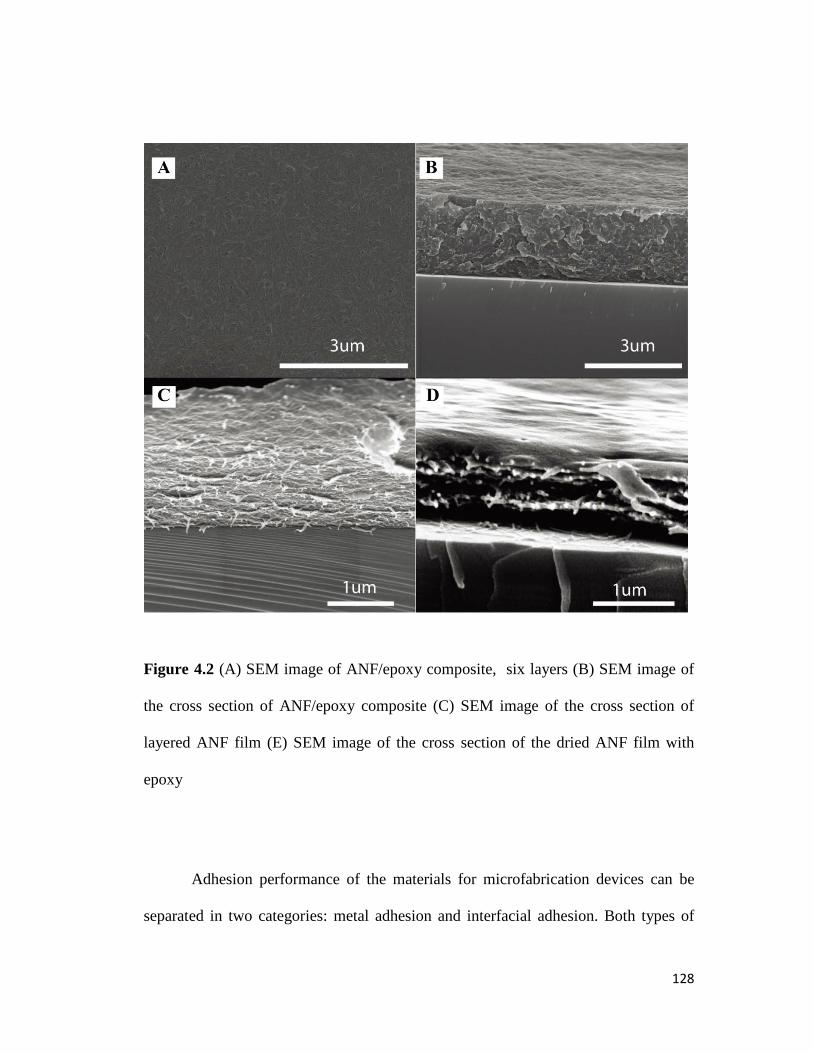
128
Figure 4.2 (A) SEM image of ANF/epoxy composite, six layers (B) SEM image of
the cross section of ANF/epoxy composite (C) SEM image of the cross section of
layered ANF film (E) SEM image of the cross section of the dried ANF film with
epoxy
Adhesion performance of the materials for microfabrication devices can be
separated in two categories: metal adhesion and interfacial adhesion. Both types of
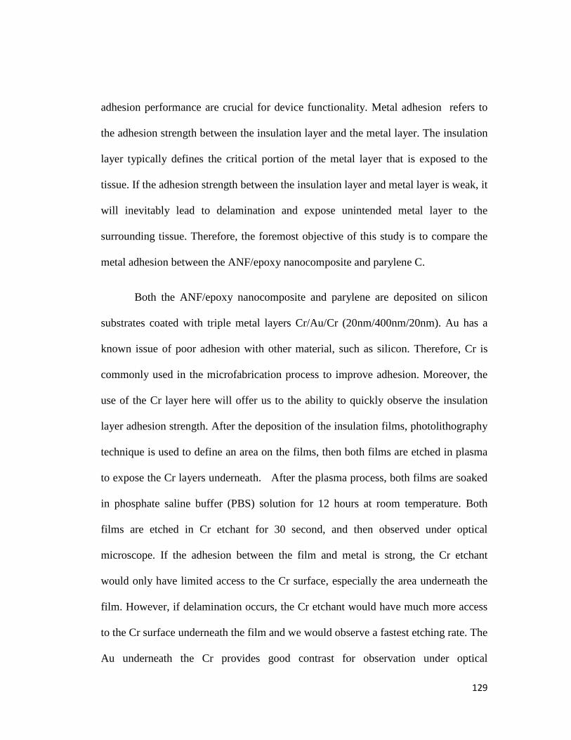
129
adhesion performance are crucial for device functionality. Metal adhesion refers to
the adhesion strength between the insulation layer and the metal layer. The insulation
layer typically defines the critical portion of the metal layer that is exposed to the
tissue. If the adhesion strength between the insulation layer and metal layer is weak, it
will inevitably lead to delamination and expose unintended metal layer to the
surrounding tissue. Therefore, the foremost objective of this study is to compare the
metal adhesion between the ANF/epoxy nanocomposite and parylene C.
Both the ANF/epoxy nanocomposite and parylene are deposited on silicon
substrates coated with triple metal layers Cr/Au/Cr (20nm/400nm/20nm). Au has a
known issue of poor adhesion with other material, such as silicon. Therefore, Cr is
commonly used in the microfabrication process to improve adhesion. Moreover, the
use of the Cr layer here will offer us to the ability to quickly observe the insulation
layer adhesion strength. After the deposition of the insulation films, photolithography
technique is used to define an area on the films, then both films are etched in plasma
to expose the Cr layers underneath. After the plasma process, both films are soaked
in phosphate saline buffer (PBS) solution for 12 hours at room temperature. Both
films are etched in Cr etchant for 30 second, and then observed under optical
microscope. If the adhesion between the film and metal is strong, the Cr etchant
would only have limited access to the Cr surface, especially the area underneath the
film. However, if delamination occurs, the Cr etchant would have much more access
to the Cr surface underneath the film and we would observe a fastest etching rate. The
Au underneath the Cr provides good contrast for observation under optical
130
microscope. The optical microscopy images after etching are shown in Figure 2. In
comparing the etch rate of Cr for both film, we can clearly observe a faster etch rate
for the parylene C coating substrate than the ANF/epoxy composite. This indicates a
stronger metal adhesion for the ANF/epoxy composite over parylene C
Figure 4.3 Metal adhesion test (A) Wet Cr etch of ANF/epoxy composite, rectangular
strip opening (B) Wet Cr etch of parylene, rectangular strip opening (C) Wet Cr etch
of ANF/epoxy composite, square opening (D) Wet Cr etch of parylene, square
opening
131
The metal adhesion test provided preliminary result on the superior adhesion
performance of the ANF/epoxy composite. Nevertheless, the adhesion performance
of the ANF composite requires more rigorous test model to further validate its
purpose in practical applications. Therefore, we design an interdigitated electrode
(IDE) approach to further test the long term adhesion performance.
The IDE structure is illustrated in Figure 3. Simply, the IDE design involves
two electrodes in a closed spatial arrangement sandwiched between two layers of the
insulation materials. This type of layered configurations is common in bioelectronic
devices. In this configuration, there are two interfacial boundary layers, shown in
Figure 3A . One is the polymer-polymer interface. If this interface has poor adhesion,
it will increase the cross-talk between the electrodes, and cause dramatic decrease in
the lateral impedance, Zlat. Another interface is the metal-polymer interface, which
was previously illustrated. The delamination of the metal-polymer interface also can
cause the decline of the Zlat. Therefore, the Zlat is a highly sensitive measurement of
the interfacial adhesion, especially from microstructures.
In order to compare the Zlat of parylene and ANF/epoxy composite, we must
fabricate the IDE on both films. We purposely design an ultrasmall and high aspect
ratio IDE electrodes (1.5um width and 700 um long) to test the photolithography limit
of the both films (Figure 3B). Parylene is known for its compatibility with
photolithography process, thus it is widely accepted as insulation materials for
implantable electronics. Therefore it is important for us to compare the ability to
132
create microscale structures on parylene and ANF/epoxy composite. The overall
structure of the IDE on parylene is shown in Figure 3B, demonstrates a successfully
fabricated IDE structures. The details of the IDE fabrication are included in the
Methods section. Then we further examine the fine electrode structures by optical
microscopy. Comparing Figure 3C and 3D, we can conclude that the same microscale
structures can be fabricated on ANF/epoxy composite as on parylene, although we
observe more roughness of the ANF/epoxy comparing to parylene under optical
microscope.

133
Figure 4.4 (A) Illustration of the interfaces in IDE (B) Fabricated IDE structure (C)
Zoom in IDE structure on parylene film (D) Zoom in IDE structure on ANF/epoxy
composite
After we establish the successful protocol to fabricate the IDE on both
substrates, we conduct long term soak test to compare the adhesion performance of
parylene and ANF/epoxy composite. The long term soak test is conducted in
phosphate saline buffer (PBS) at 37 C. 16 IDE electrodes for from each type of the
films were soaked in the PBS for 45 days in a temperature controlled water bath.
134
Prior to the soaking test, the impedance of the electrodes in dry state is also measured.
The measurement protocol is also described in the Materials and Methods section. In
Figure 4A, it shows the Zlat measurements of parylene and ANF/epoxy after 45 days
of soak testing. For comparison purpose, we also plot the dry state Zlat measurement.
Because there is no difference in dry Zlat measurement for parylene and ANF/epoxy
composite, only one dry Zlat measurement is plotted on the graph. The dry impedance
measurement follows typical pure capacitor behavior in a circuit analogy. As we
observe in Figure 4A, the dry impedance in low frequency is extremely high, in the
Gohm range. This indicates that the electrodes are well insulated from each other by
the thin films. The magnitude of the capacitance is positively proportional to the
frequency. And the magnitude of the impedance is inversely proportional to the
capacitance. Therefore, the impedance of the system decreases as the frequency
increase. Moreover, the dry impedance measurement is linearly correlated with the
frequency on a logarithmic scale plot. This also indicates a capacitor behavior since
capacitors follow a power law relationship with frequency. All three impedance
measurements follow the same trend over frequency. However, the Zlat measurement
in the lower frequency after soak test decreases one or two magnitudes compare to the
dry impedance test. This is expected because the long term soak test will induce
compromises in the interface. Furthermore, we observed that the impedance over
frequency does not follow a linear trend on the logarithmic scale after the soak test in
either case. As we mentioned previously, the system does not behavior as a pure
capacitor anymore and additional circuit components need to be added to describe the
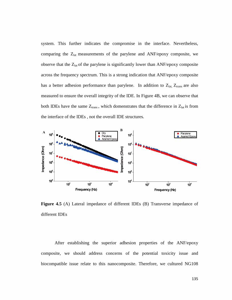
135
system. This further indicates the compromise in the interface. Nevertheless,
comparing the Zlat measurements of the parylene and ANF/epoxy composite, we
observe that the Zlat of the parylene is significantly lower than ANF/epoxy composite
across the frequency spectrum. This is a strong indication that ANF/epoxy composite
has a better adhesion performance than parylene. In addition to Zlat, Ztrans are also
measured to ensure the overall integrity of the IDE. In Figure 4B, we can observe that
both IDEs have the same Ztrans , which domenstrates that the difference in Zlat is from
the interface of the IDEs , not the overall IDE structures.
Figure 4.5 (A) Lateral impedance of different IDEs (B) Transverse impedance of
different IDEs
After establishing the superior adhesion properties of the ANF/epoxy
composite, we should address concerns of the potential toxicity issue and
biocompatible issue relate to this nanocomposite. Therefore, we cultured NG108
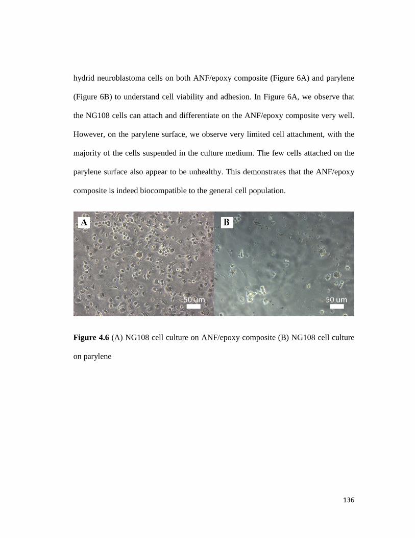
136
hydrid neuroblastoma cells on both ANF/epoxy composite (Figure 6A) and parylene
(Figure 6B) to understand cell viability and adhesion. In Figure 6A, we observe that
the NG108 cells can attach and differentiate on the ANF/epoxy composite very well.
However, on the parylene surface, we observe very limited cell attachment, with the
majority of the cells suspended in the culture medium. The few cells attached on the
parylene surface also appear to be unhealthy. This demonstrates that the ANF/epoxy
composite is indeed biocompatible to the general cell population.
Figure 4.6 (A) NG108 cell culture on ANF/epoxy composite (B) NG108 cell culture
on parylene

137
Figure 4.7 Live/Dead Assay of NG108 cells on various substrates. (Green:Live Red:
Dead) (A) NG108 cell culture on tissue culture coverslip glass (B) NG108 cell culture
on parylene (C) NG108 cell culture on ANF/epoxy (D) NG108 cell culture on
ANF/epoxy treated with 70% ethanol solution.
Live/Dead assay are also performed to understand viability of the cells on the
substrates. NG108 cells are cultured three different substrates: regular cover slip glass
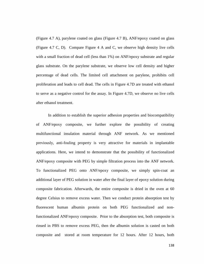
138
(Figure 4.7 A), parylene coated on glass (Figure 4.7 B), ANF/epoxy coated on glass
(Figure 4.7 C, D). Compare Figure 4 A and C, we observe high density live cells
with a small fraction of dead cell (less than 1%) on ANF/epoxy substrate and regular
glass substrate. On the parylene substrate, we observe low cell density and higher
percentage of dead cells. The limited cell attachment on parylene, prohibits cell
proliferation and leads to cell dead. The cells in Figure 4.7D are treated with ethanol
to serve as a negative control for the assay. In Figure 4.7D, we observe no live cells
after ethanol treatment.
In addition to establish the superior adhesion properties and biocompatibility
of ANF/epoxy composite, we further explore the possibility of creating
multifunctional insulation material through ANF network. As we mentioned
previously, anti-fouling property is very attractive for materials in implantable
applications. Here, we intend to demonstrate that the possibility of functionalized
ANF/epoxy composite with PEG by simple filtration process into the ANF network.
To functionalized PEG onto ANF/epoxy composite, we simply spin-coat an
additional layer of PEG solution in water after the final layer of epoxy solution during
composite fabrication. Afterwards, the entire composite is dried in the oven at 60
degree Celsius to remove excess water. Then we conduct protein absorption test by
fluorescent human albumin protein on both PEG functionalized and non-
functionalized ANF/epoxy composite. Prior to the absorption test, both composite is
rinsed in PBS to remove excess PEG, then the albumin solution is casted on both
composite and stored at room temperature for 12 hours. After 12 hours, both
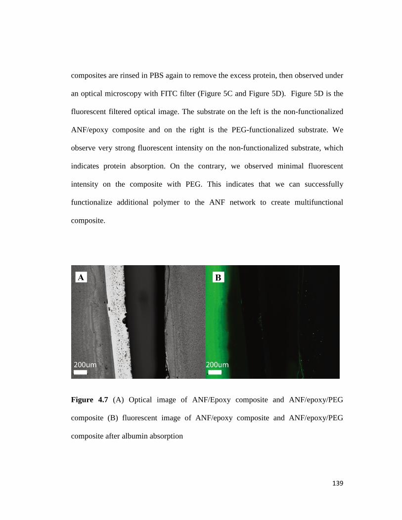
139
composites are rinsed in PBS again to remove the excess protein, then observed under
an optical microscopy with FITC filter (Figure 5C and Figure 5D). Figure 5D is the
fluorescent filtered optical image. The substrate on the left is the non-functionalized
ANF/epoxy composite and on the right is the PEG-functionalized substrate. We
observe very strong fluorescent intensity on the non-functionalized substrate, which
indicates protein absorption. On the contrary, we observed minimal fluorescent
intensity on the composite with PEG. This indicates that we can successfully
functionalize additional polymer to the ANF network to create multifunctional
composite.
Figure 4.7 (A) Optical image of ANF/Epoxy composite and ANF/epoxy/PEG
composite (B) fluorescent image of ANF/epoxy composite and ANF/epoxy/PEG
composite after albumin absorption
140
4.5 Conclusion
We demonstrate the possibility of utilizing ANF as a frame network to create
multifunctional insulation materials. We conduct multiple adhesion tests to
systematically evaluate the adhesion performance of ANF/epoxy composite. The
results from metal etching test and long term soak test indicate that ANF/epoxy
composite indeed has a superior adhesion performance than parylene. Neural cell
culture experiments are also performed to validate the biocompatibility of the
ANF/epoxy composite. Lastly, the robustness of the ANF network allows us to create
gradient composite with epoxy and PEG. Protein absorption test indicates that PEG
can be successfully functionalized on top of the epoxy resin within the ANF network.
This demonstrates that this approach of utilized ANF network can open up
opportunities for multifunctional material design. Although our study revealed this
new composite approach to design superior insulation materials, further studies on
using this ANF/epoxy for functional implantable electronics are required to establish
the feasibility of this composite approach for in vivo applications.
4.6 References
1. Berger, T. W.; Baudry, M.; Brinton, R. D.; Liaw, J. S.; Marmarelis, V. Z.;
Park, A. Y.; Sheu, B. J.; Tanguay, A. R., Brain-Implantable Biomimetic Electronics
as the Next Era in Neural Prosthetics. P Ieee 2001, 89, 993-1012.
2. House, W. F., Cochlear Implants. Ann Oto Rhinol Laryn 1976, 85, 3-93.
141
3. House, W. F., Cochlear Implants - Its Time to Rethink. Am J Otol 1994, 15,
573-587.
4. Perlmutter, J. S.; Mink, J. W., Deep Brain Stimulation. Annu Rev Neurosci
2006, 29, 229-257.
5. Wise, K. D., Silicon Microsystems for Neuroscience and Neural Prostheses.
Engineering in Medicine and Biology Magazine, IEEE 2005, 24, 22-29.
6. Maynard, E. M.; Nordhausen, C. T.; Normann, R. A., The Utah Intracortical
Electrode Array: A Recording Structure for Potential Brain-Computer Interfaces.
Electroencephalography and clinical neurophysiology 1997, 102, 228-39.
7. Polikov, V. S.; Tresco, P. A.; Reichert, W. M., Response of Brain Tissue to
Chronically Implanted Neural Electrodes. J Neurosci Meth 2005, 148, 1-18.
8. Hollenberg, B. A.; Richards, C. D.; Richards, R.; Bahr, D. F.; Rector, D. M.,
A Mems Fabricated Flexible Electrode Array for Recording Surface Field Potentials.
J Neurosci Methods 2006, 153, 147-53.
9. Fan, W.; Maesoon, I.; Euisik, Y. In A Flexible Fish-Bone-Shaped Neural
Probe Strengthened by Biodegradable Silk Coating for Enhanced Biocompatibility,
Solid-State Sensors, Actuators and Microsystems Conference (TRANSDUCERS),
2011 16th International, 5-9 June 2011; 2011; pp 966-969.
10. Krulevitch, P.; Polla, D. L.; Maghribi, M. N.; Hamilton, J. Flexible Electrode
Array for Artificial Vision. 2001-992248
2003097166, 20011116., 2003.
142
11. Stieglitz, T.; Gross, M., Flexible Biomems with Electrode Arrangements on
Front and Back Side as Key Component in Neural Prostheses and Biohybrid Systems.
Sens. Actuators, B 2002, B83, 8-14.
12. Takeuchi, S.; Suzuki, T.; Mabuchi, K.; Fujita, H., 3d Flexible Multichannel
Neural Probe Array. Journal of Micromechanics and Microengineering 2004, 14,
104-107.
13. Wise, K. D.; Angell, J. B.; Starr, A., An Integrated-Circuit Approach to
Extracellular Microelectrodes. Biomedical Engineering, IEEE Transactions on 1970,
BME-17, 238-247.
14. Wilke, R. G. H.; Moghadam, G. K.; Lovell, N. H.; Suaning, G. J.; Dokos, S.,
Electric Crosstalk Impairs Spatial Resolution of Multi-Electrode Arrays in Retinal
Implants. J Neural Eng 2011, 8.
15. Bowman, L.; Meindl, J. D., The Packaging of Implantable Integrated Sensors.
Ieee T Bio-Med Eng 1986, 33, 248-255.
16. Seymour, J. P.; Elkasabi, Y. M.; Chen, H. Y.; Lahann, J.; Kipke, D. R., The
Insulation Performance of Reactive Parylene Films in Implantable Electronic Devices.
Biomaterials 2009, 30, 6158-67.
17. Onuki, Y.; Bhardwaj, U.; Papadimitrakopoulos, F.; Burgess, D. J., A Review
of the Biocompatibility of Implantable Devices: Current Challenges to Overcome
Foreign Body Response. Journal of diabetes science and technology 2008, 2, 1003-15.
18. Suzuki, T.; Kopia, G.; Hayashi, S.; Bailey, L. R.; Llanos, G.; Wilensky, R.;
Klugherz, B. D.; Papandreou, G.; Narayan, P.; Leon, M. B.; Yeung, A. C.; Tio, F.;
143
Tsao, P. S.; Falotico, R.; Carter, A. J., Stent-Based Delivery of Sirolimus Reduces
Neointimal Formation in a Porcine Coronary Model. Circulation 2001, 104, 1188-93.
19. Scheller, B.; Hehrlein, C.; Bocksch, W.; Rutsch, W.; Haghi, D.; Dietz, U.;
Bohm, M.; Speck, U., Treatment of Coronary in-Stent Restenosis with a Paclitaxel-
Coated Balloon Catheter. The New England journal of medicine 2006, 355, 2113-24.
20. Zilberman, M.; Elsner, J. J., Antibiotic-Eluting Medical Devices for Various
Applications. J Control Release 2008, 130, 202-215.
21. He, W.; McConnell, G. C.; Bellamkonda, R. V., Nanoscale Laminin Coating
Modulates Cortical Scarring Response around Implanted Silicon Microelectrode
Arrays. Journal of neural engineering 2006, 3, 316-26.
22. He, W.; McConnell, G. C.; Schneider, T. M.; Bellamkonda, R. V., A Novel
Anti-Inflammatory Surface for Neural Electrodes. Adv. Mater. 2007, 19, 3529-3533.
23. Meng, E.; Tai, Y. C., Parylene Etching Techniques for Microfluidics and
Biomems. Proc Ieee Micr Elect 2005, 568-571.
24. Lahann, J., Vapor-Based Polymer Coatings for Potential Biomedical
Applications. Polym Int 2006, 55, 1361-1370.
25. Yasuda, H.; Yu, Q. S.; Chen, M., Interfacial Factors in Corrosion Protection:
An Eis Study of Model Systems. Prog Org Coat 2001, 41, 273-279.
26. Yamagishi, F. G., Investigation of Plasma-Polymerized Films as Primers for
Parylene-C Coatings on Neural Prosthesis Materials. Thin Solid Films 1991, 202, 39-
50.
144
27. Sharma, A. K.; Yasuda, H., Effect of Glow-Discharge Treatment of Substrates
on Parylene-Substrate Adhesion. J Vac Sci Technol 1982, 21, 994-998.
28. Metzen, R.; Stieglitz, T., The Effects of Annealing on Mechanical, Chemical,
and Physical Properties and Structural Stability of Parylene C. Biomed Microdevices
2013, 15, 727-735.
29. Nicolelis, M. A.; Dimitrov, D.; Carmena, J. M.; Crist, R.; Lehew, G.; Kralik, J.
D.; Wise, S. P., Chronic, Multisite, Multielectrode Recordings in Macaque Monkeys.
Proceedings of the National Academy of Sciences of the United States of America
2003, 100, 11041-6.
30. Xindong, L.; McCreery, D. B.; Carter, R. R.; Bullara, L. A.; Yuen, T. G. H.;
Agnew, W. F., Stability of the Interface between Neural Tissue and Chronically
Implanted Intracortical Microelectrodes. Rehabilitation Engineering, IEEE
Transactions on 1999, 7, 315-326.
31. Stieglitz, T., Hansjorg, B., Schuettler, M. and Meyer, J.-U, Micromachined,
Polyimide-Based Devices for Flexible Neural Interfaces. Biomedical Microdevices
2000, 2, 283-294.
32. Yang, M.; Cao, K. Q.; Sui, L.; Qi, Y.; Zhu, J.; Waas, A.; Arruda, E. M.;
Kieffer, J.; Thouless, M. D.; Kotov, N. A., Dispersions of Aramid Nanofibers: A New
Nanoscale Building Block. Acs Nano 2011, 5, 6945-6954.
33. Cao, K. Q.; Siepermann, C. P.; Yang, M.; Waas, A. M.; Kotov, N. A.;
Thouless, M. D.; Arruda, E. M., Reactive Aramid Nanostructures as High-

145
Performance Polymeric Building Blocks for Advanced Composites. Adv Funct Mater
2013, 23, 2072-2080.
146
Chapter 5
Flexible High Performance Nanocomposite Microelectrodes for Neural Interface
5.1 Abstract
Mechanical flexibility of electrode materials is important to mitigate the
chronic inflammation response of implantable neural electrodes. Gold
nanocomposites featuring low Young’s modulus, high electrical conductivity, and
excellent electrochemical performance could be a promising high performance
material for neural electrodes. Nevertheless, traditional flexible insulators suffer from
inferior adhesive properties, which ultimately lead to devices failure. Aramid
nanofiber composites have demonstrated excellent adhesion on metal, and could
improve the chronic functionality of implantable devices. This study demonstrates the
direct integration of two high performance nanocomposite materials to fabricate
microelectrodes, as well as validates the in vivo functionality of the integrated
nanocomposite electrode
147
5.2 Introduction
Implantable electrodes have been the essential technological component for
many neural interface systems.1-6 Recent developments in brain computer interface
offer us the possibility to extract neural signals from the brain and control external
devices.7-9 This could have tremendous impact on patients suffering from neural
diseases and traumas. Particularly, recording electrodes are commonly used to detect
neural signals and transport this signal to external electrical components.5 The
performance and reliability of implantable recording electrodes are crucial for
maintaining an efficient and sustainable brain computer interface.10
Metal microwire electrodes and silicon microelectrodes have achieved
enormous success in early clinical applications. Metal microwire arrays were first
developed for animal experiments due to the simplicity of array assembly and high
electrical conductivity of the metals.11-14 After the development of metal microwire
arrays, the next technological innovation in microelectrodes came from the silicon
based microfabrication process,15-18 when more precise and sophisticated electrode
arrays were required. Indeed, we have much control over shape, size, position,
density, and materials of electrodes today. Advanced functionalities, such as wireless
transmission19, 20 and on-chip signal processing21 are also available. Nevertheless,
neither type of the electrode sustains its functionality for more than a year (for over
a year? For a few months? How long do they normally last?).10 This issue of chronic
device failure has significantly hindered the future development of the brain computer
interface and its applications in clinical setting.
148
There are many failure modes for implantable recording electrodes. This
discussion focuses on two major device failure modes: mechanical mismatch at the
tissue/electrode interface and delamination of insulating materials. Mechanical
mismatch between the electrode and brain tissue has been recognized as a key issue
for chronic device functionality.10, 22 Brain tissue is very soft and under dynamic
motion constantly.23-25 Typical metal or silicon electrodes are stiff materials and have
large mechanical mismatch with brain tissue. This mechanical mismatch will
consistently interrupt the brain-blood barrier and initiate immune response.22, 24
Chronic immune response will inevitably lead to the formation of scar tissue and
create barriers between electrodes and targeted neurons.26 Moreover, in order to
obtain neural signals from a single neuron, the electrode has to be in close spatial
arrangement with the targeted neuron, a distance of approximately 100 um.27 Rigid
electrodes are more likely to damage nearby neurons during dynamic movement of
the brain. This also contributes to signal loss and recording inconsistency of chronic
neural electrodes. Flexible electrodes have been developed to mitigate this
mechanical mismatch.28-33 These electrodes typically are fabricated by using
polymers as a backbone and metal thin film as an electrical conductor. These types of
electrodes are much more flexible than silicon or metal wires. In addition , the
combined mechanical properties of polymer and metal are still much higher than
brain tissue. Nanocomposite materials could be an alternative approach to fabricating
electrodes. By incorporating conductive nanomaterials into a polymer matrix, it is
possible to create flexible nanocomposites with high electrical conductivity. Recent
149
studies have demonstrated that tailored nanocomposites can have high electrical
conductivity,34 high electrochemical performance,35 and the feasibility of fabricating
neural electrodes.36 Particularly, gold nanoparticle (Au NP) nanocomposites have
exhibited both high electrical conductivity and outstanding interfacial electrochemical
properties.37 These properties indicate that gold nanocomposites could be an excellent
choice for neural electrode material. However, gold nanocomposites have not yet
been fabricated into in vivo neural electrodes.
In addition to mechanical mismatch, delamination of the insulating material
can also contribute to device failure, especially for flexible devices.38 Insulating
materials are crucial for device functionality because they define the electrical active
area of the neural electrodes. If the delamination occurs at the electrical/insulating
material interface, the active area of the electrode will be altered. This greatly affects
the signal reception of the electrodes and leads to device failure. Moreover,
engineering flexible neural electrodes, requires not only the electrically conductive
materials to be flexible, but also the insulating materials. It is very important to
develop flexible materials with great adhesion. Parylene is a common material for
flexible electronics; however, it has challenges with metal adhesion due to its
hydrophobic nature.39-41 Nanocomposites based on aramid nanofibers (ANF) and
epoxy have shown great adhesion and biocompatibility in recent studies. Thus, it is
advantageous to incorporate ANF/epoxy nanocomposites into functional neural
electrodes.
In this study, we integrate both Au NP nanocomposites and ANF
nanocomposites to create all nanocomposite electrodes. We first establishe the
150
protocol to fabricate nanocomposite electrodes, then we demonstrate its functionality
in vivo.
5.3 Materials and Method
Right-twisted bulk Kevlar 69 was purchased from Thread Exchange. System
2000 Epoxy Resin was purchased from Fibre Glast Developments Corporation. All
other chemicals were obtained from Sigma-Aldrich
5.3.1 ANF Nanofiber Dispersion
1g of purchased aramid thread was dissolved in 100ml of DMSO with 4 g of
KOH to prepare a 10mg/ml ANF nanofiber dispersion. The solution was stirred in a
sealed container at room temperature for a week to ensure the complete dissolution of
the nanofiber.
5.3.2 ANF/Epoxy Nanocomposite
The nanocomposite film was created through a spin-coating assisted
deposition process. 1ml of as-prepared ANF nanofiber dispersion was spin-coated on
a 1.5-inch by-1.5 inch silicon oxide wafer at 1000 rpm. After spin coating, the film
was rinsed with water to remove the excess DMSO in the film, then spin-coated at
1000 rpm. After rinsing with water, 1 ml of 3% epoxy resin in acetone was spin-
151
coated on top of the ANF nanofiber film and dried in the oven at 100 degrees Celsius
for 1 min. In order to achieve a pinhole-free film, the epoxy resin solution was spin-
coated again after the first layer of the epoxy resin solution. The process was repeated
until the desired film thickness was achieved. Typically, six repeated cycles results in
a 3 um thick film.
5.3.3 Synthesis of Gold Nanoparticles
The synthesis of Au NPs followed the standard citrate reduction method.
Briefly, 90 mg of HAuCl4 were dissolved in 500 ml of water. The solution was
heated on a hot plate until boiling. Then 25ml of 0.1% sodium citrate aqueous
solution was added to the gold salt solution. The mixture was stirred and reboiled on a
hot plate. After 20 minutes, the solution became a red color, which indicated the
formation of Au NPs. The Au NPs were concentrated 10X by centrifuging at 9000
rpm for 50 minute and removing 90% of the supernatant
5.3.4 Layer-by-Layer Assembly of Au NP film
LBL assembly was initially carried out on microscope glass slides cleaned in
piranha solution overnight and then thoroughly rinsed with deionized water prior to
use. For LBL assembly, a glass slide was immersed in 0.1 wt % solution of PDDA for
5 min, rinsed with DI water for 1 min, dried, and then immersed in concentrated Au
152
NP solution for 10 min, rinsed for 1 min, and dried again. The procedure was then
repeated with PDDA and Au NP solution.
5.3.5 Electrode Fabrication
2µm ANF/epoxy nanocomposite was first deposited via spin-coating on a
silicon wafer with 2 µm thermal oxide. The first layer of ANF/epoxy nanocomposite
served as the bottom insulating layer for the electrodes. Then 100 nm Au NP
nanocomposite was deposited on the ANF/epoxy layer by using the layer-by-layer
(LBL) assembly method. After the Au NP composite deposition, positive photoresist
(SPR220-3.0, Rohm Haas) was spin coated and exposed by the first mask on the gold
composite. After developing the photoresist, the entire substrate was etched in gold
etchant (Gold Etchant TFA, Transene Company, Inc.) for 20 seconds to pattern the
base layer of the neural electrodes. After wet etching, a layer of chromium was
deposited onto the base layer to protect the Au NP composite. Next, a second layer of
ANF/epoxy composite was deposited. This served as the top insulating layer for the
neural probe. Then, positive photoresist was spin-coated again and exposed by the
second mask on top of the second layer of parylene-C. The entire substrate was
etched in oxygen with 10% sulfur hexafluoride. The second mask created the outline
for the final electrode shape and opened the functional Au NP sites at the tip of the
electrodes. Lastly, copper wires were attached onto the electrodes by silver epoxy
paste. The entire device was then released from the silicon wafer by hydrogen
fluoride.
153
5.3.6 Scanning Electron Microscopy (SEM)
SEM images were obtained using a FEI Nova Nanolab SEM at a 10kV
accelerating voltage. The samples were sputter coated with gold prior to SEM
imaging.
5.3.7 Electrochemical Impedance Spectroscopy (EIS)
EIS was carried out on an Autolab PGSTAT 12. Frequency Response
Analyzer software (EcoChemie, Utrecht, Netherlands) was used to record impedance
spectra of the electrodes. A solution of 1 M phosphate buffered saline (PBS, pH = 7)
was used as an electrolyte in a three-electrode configuration. The working electrode
was connected to the electrode site. The counter electrode was connected to a gold
foil immersed in PBS, and an Ag/AgCl reference electrode was immersed in PBS. An
AC sinusoidal signal of 25 mV in amplitude was used to record the impedance over a
frequency range of 10−32000 Hz.
5.3.8 Craniotomy Preparation
Adult male Sprague-Dawley rats (Charles River Laboratories) 550-600 g
were anesthetized with 2% isoflurane and 1mg/ml ketamine. The depth of anesthesia
was observed by monitoring heart rate and blood oxygen saturation. The animal was
placed into a stereotaxic frame and a 2 mm-by-2 mm craniotomy was made over the
visual cortex. Once the dura was incised and resected, the animal brain was ready for
implantation.
154
5.3.9 In-vivo Electrophysiological Recording
Electrophysiological data was recorded using a TDT RX5 Pentusa Recording
System (Tucker-Davis Technologies, Alachua, FL). These neuronal signals were
acquired through a head-stage buffer amplifier to avoid signal loss in data
transmission. Signals were sequentially filtered by an anti-aliasing filter in the
preamplifier, digitized at a ~ 25-kHz sampling rate, and digitally band-pass filtered
from 300 to 5000 Hz. Wideband signals were acquired to capture both spiking and
local field potential (LFP) activity. Signals were continuously recorded for 3 seconds:
a 1s at the initial off state, then a 1s during the drifting grating movie followed by a 1s
long “black screen”. Neural recording segments were analyzed offline using custom
automated MATLAB (Mathworks Inc., MA) script.
5.4 Results and Discussion
The integration of Au NP nanocomposites and ANF/epoxy composites is
essential for fabricating all composite electrodes. Therefore, we first evaluate the
layer-by-layer (LBL) assembly of the Au NP composite on top of the ANF/epoxy
composite. The LBL process relies on the charge interaction of material components.
For Au NP nancomposites, we choose a biocompatible and positive polyelectrolyte,
polydiallydimethylammonium chloride (PDDA), to pair with negative charged Au
NP, which is stabilized with sodium citrate. The substrate for the LBL process should
also have certain charge, in order to initiate the assembly process. We first create a
six ANF/epoxy composite on a silicon wafer with 2 µm thermal oxide according to
the established protocol. The epoxy resin in the ANF network would give the
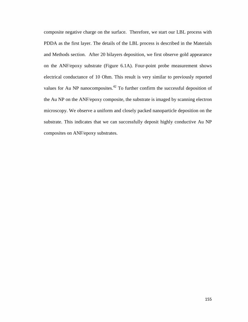
155
composite negative charge on the surface. Therefore, we start our LBL process with
PDDA as the first layer. The details of the LBL process is described in the Materials
and Methods section. After 20 bilayers deposition, we first observe gold appearance
on the ANF/epoxy substrate (Figure 6.1A). Four-point probe measurement shows
electrical conductance of 10 Ohm. This result is very similar to previously reported
values for Au NP nanocomposites.42 To further confirm the successful deposition of
the Au NP on the ANF/epoxy composite, the substrate is imaged by scanning electron
microscopy. We observe a uniform and closely packed nanoparticle deposition on the
substrate. This indicates that we can successfully deposit highly conductive Au NP
composites on ANF/epoxy substrates.
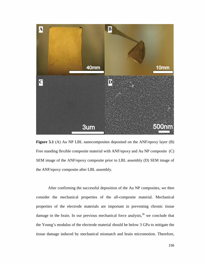
156
Figure 5.1 (A) Au NP LBL nanocomposites deposited on the ANF/epoxy layer (B)
Free standing flexible composite material with ANF/epoxy and Au NP composite (C)
SEM image of the ANF/epoxy composite prior to LBL assembly (D) SEM image of
the ANF/epoxy composite after LBL assembly.
After confirming the successful deposition of the Au NP composites, we then
consider the mechanical properties of the all-composite material. Mechanical
properties of the electrode materials are important in preventing chronic tissue
damage in the brain. In our previous mechanical force analysis,36 we conclude that
the Young’s modulus of the electrode material should be below 3 GPa to mitigate the
tissue damage induced by mechanical mismatch and brain micromotion. Therefore,
157
we should first assess the Young’s modulus of the composite material. After
deposition of gold nanocomposite, the entire substrate is soaked in 1% glutaraldyhyde
for 1 hour to cross-link the Au NP composite. This process strengthens the
interparticle connection in the composite, which is important for the microfabricaton
process. After cross-linking, the entire ANF/epoxy composite with LBL-assembled
nanoparticles is lifted off from the silicon substrate (Figure 6.1B). A mechanical
tensile test is conducted to measure the Young’s modulus of the composite (Figure
5.2). The Young’s modulus of the composite is 2.8 GPa, which is suitable for
electrode fabrication.
Figure 5.2 (A) Tensile test result of the all-composite electrode material (B)
Magnitude of the impedance for typical as-fabricated electrodes.
The conductivity measurement and mechanical test demonstrate that this
particular composite material is a promising platform to fabricate implantable
electrodes. However, fabrication of this composite material requires special analysis
to develop appropriate process protocol. First, both composite materials contain
158
organic components. ANF/epoxy composite is etched by oxygen plasma during the
fabrication process. Regular gold film in traditional electrodes is not typically
affected by the oxygen plasma process. In the case of composite electrodes, the
electrically active material is the Au NP composite. Densely packed Au NPs are
connected by thin polymer, which offers mechanical flexibility and high electrical
conductivity. However, this Au NP composite will be affected by the high voltage
oxygen plasma. We need to resolve the issue of non-selectivity during the oxygen
plasma process. In this study, we applied a combination of etch stop and crosslink
techniques to resolve this issue. The Au NP composite is first cross-linked to
improve connectivity of the nanoparticle in the composite. Then we also use an
additional layer of Cr to protect the nanocomposite from the oxygen plasma. The
process protocol is described in detail in the Materials and Methods section.
By using this tailored fabrication process, we are able to produce high yield
electrodes from the substrate. Figure 5.3B shows an all-composite electrode lifted off
from the silicon substrate. In order to confirm the robustness of the Au NP composite,
optical microscopy images are taken before and after the electrode liftoff process
from the silicon substrate (Figure 5.3C and Figure 5.3D). Compare to both images,
we can conclude that there is no delamination or cracking of the Au NP composite.
Prior to in vivo study, the electrochemical performance of the electrodes are
evaluated to verify their functionality. Electrochemical impedance of the electrodes
provides information related to the efficiency of the tissue/electrode interface. The
typical impedance requirement for recording electrodes is about 1Mohm. The
impedance of the as-fabricated electrodes is measured by a frequency analyzer from
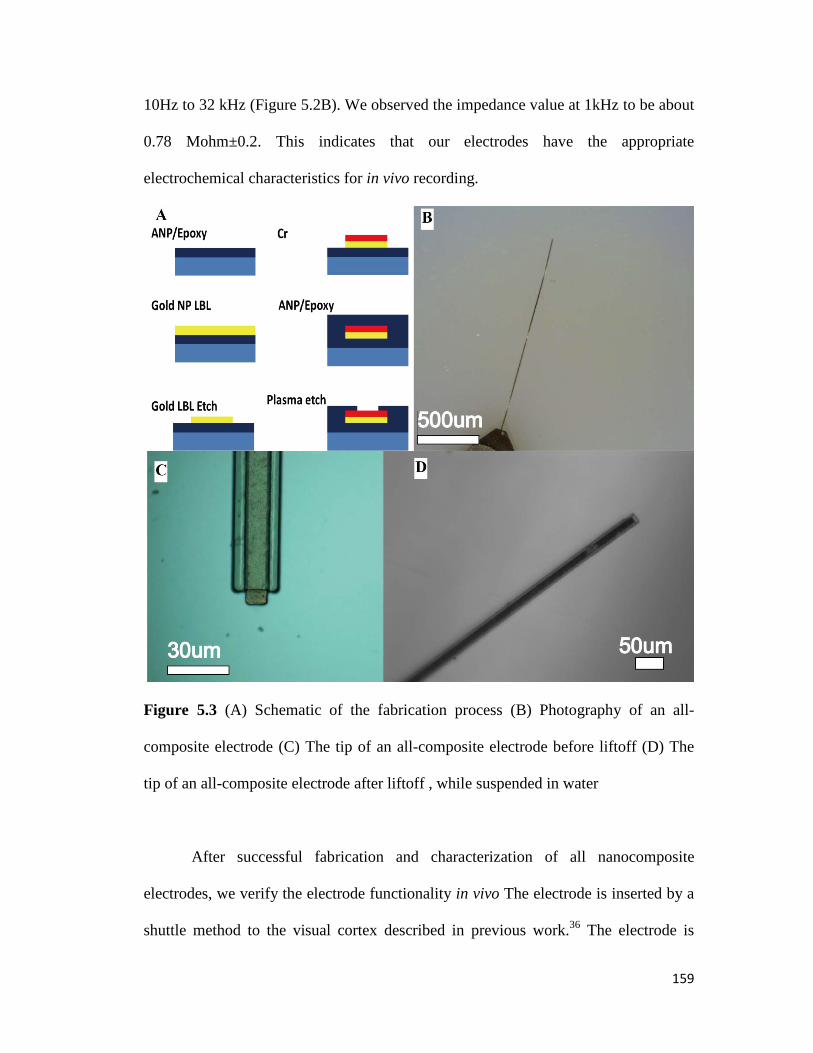
159
10Hz to 32 kHz (Figure 5.2B). We observed the impedance value at 1kHz to be about
0.78 Mohm±0.2. This indicates that our electrodes have the appropriate
electrochemical characteristics for in vivo recording.
Figure 5.3 (A) Schematic of the fabrication process (B) Photography of an all-
composite electrode (C) The tip of an all-composite electrode before liftoff (D) The
tip of an all-composite electrode after liftoff , while suspended in water
After successful fabrication and characterization of all nanocomposite
electrodes, we verify the electrode functionality in vivo The electrode is inserted by a
shuttle method to the visual cortex described in previous work.36 The electrode is
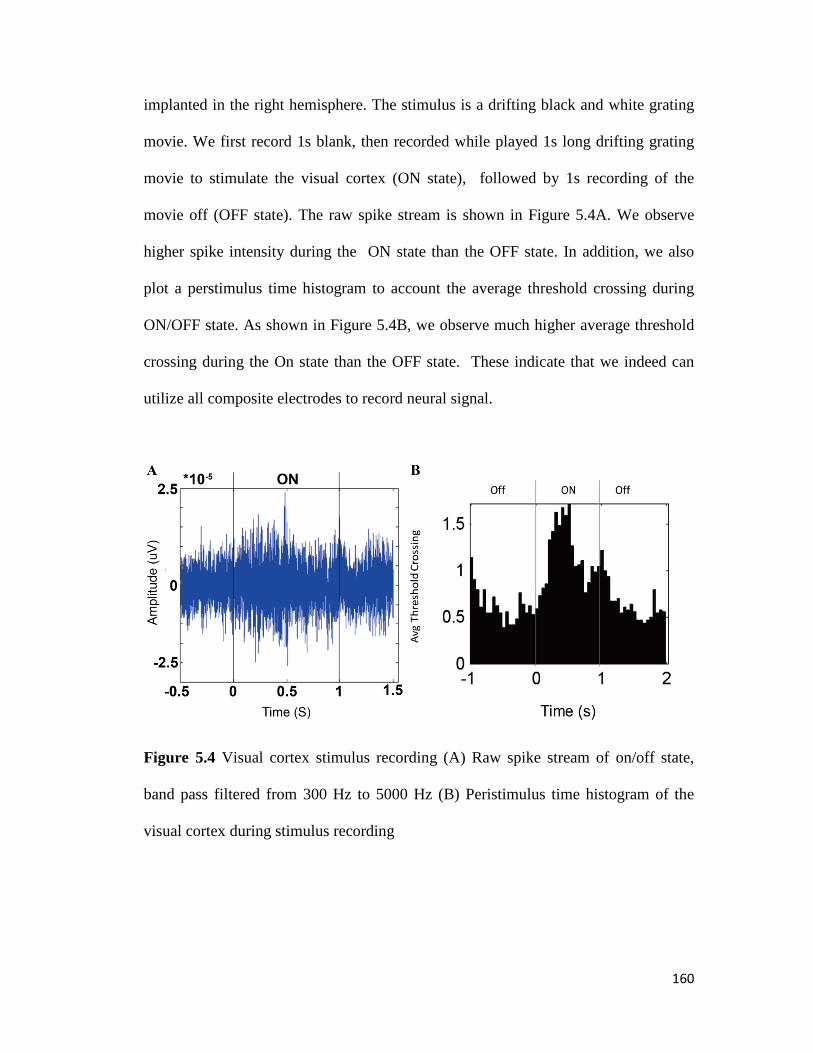
160
implanted in the right hemisphere. The stimulus is a drifting black and white grating
movie. We first record 1s blank, then recorded while played 1s long drifting grating
movie to stimulate the visual cortex (ON state), followed by 1s recording of the
movie off (OFF state). The raw spike stream is shown in Figure 5.4A. We observe
higher spike intensity during the ON state than the OFF state. In addition, we also
plot a perstimulus time histogram to account the average threshold crossing during
ON/OFF state. As shown in Figure 5.4B, we observe much higher average threshold
crossing during the On state than the OFF state. These indicate that we indeed can
utilize all composite electrodes to record neural signal.
Figure 5.4 Visual cortex stimulus recording (A) Raw spike stream of on/off state,
band pass filtered from 300 Hz to 5000 Hz (B) Peristimulus time histogram of the
visual cortex during stimulus recording
161
5.5 Conclusion
The next generation of neural prosthetic devices requires mechanically
flexible materials with outstanding electrochemical performance to mitigate chronic
inflammation and tissue damage. Besides reduction of chronic inflammation,
implantable devices also need biocompatible and strongly adhesive insulating
material to maintain long term functionality under physiological conditions. This
research combines two composite materials that have demonstratedthe appropriate
properties necessary for neural prosthetic devices. We design a specific process to
integrate these two materials. Due to the successful integration of these two
nanocomposites, we can successfully fabricate functional electrodes with required
electrochemical performance for neural recording. The functionality of the electrodes
is further validated by in vivo acute recording experimentation. This study
demonstrates the possibility to utilize nanocomposites for all aspects of neural
electrodes. Further study related to chronic neural recording and histology are
necessary to establish the efficacy of these new types of neural electrodes.
5.6 References
1. Banks, D., Neurotechnology. Engineering Science and Education Journal
1998, 7, 135-144.
2. Barinaga, M., Turning Thoughts into Actions. Science 1999, 286, 888-90.
3. Kotov, N. A.; Winter, J. O.; Clements, I. P.; Jan, E.; Timko, B. P.; Campidelli,
S.; Pathak, S.; Mazzatenta, A.; Lieber, C. M.; Prato, M.; Bellamkonda, R. V.; Silva, G.

162
A.; Kam, N. W. S.; Patolsky, F.; Ballerini, L., Nanomaterials for Neural Interfaces.
Adv Mater 2009, 21, 3970-4004.
4. Schwartz, A. B., Cortical Neural Prosthetics. Annual review of neuroscience
2004, 27, 487-507.
5. Cogan, S. F., Neural Stimulation and Recording Electrodes. Annu. Rev.
Biomed. Eng. 2008, 10, 275-309.
6. Hatsopoulos, N. G.; Donoghue, J. P., The Science of Neural Interface Systems.
Annual review of neuroscience 2009, 32, 249-66.
7. Velliste, M.; Perel, S.; Spalding, M. C.; Whitford, A. S.; Schwartz, A. B.,
Cortical Control of a Prosthetic Arm for Self-Feeding. Nature 2008, 453, 1098-101.
8. Collinger, J. L.; Wodlinger, B.; Downey, J. E.; Wang, W.; Tyler-Kabara, E. C.;
Weber, D. J.; McMorland, A. J.; Velliste, M.; Boninger, M. L.; Schwartz, A. B.,
High-Performance Neuroprosthetic Control by an Individual with Tetraplegia. Lancet
2013, 381, 557-64.
9. Hochberg, L. R.; Serruya, M. D.; Friehs, G. M.; Mukand, J. A.; Saleh, M.;
Caplan, A. H.; Branner, A.; Chen, D.; Penn, R. D.; Donoghue, J. P., Neuronal
Ensemble Control of Prosthetic Devices by a Human with Tetraplegia. Nature 2006,
442, 164-71.
10. Polikov, V. S.; Tresco, P. A.; Reichert, W. M., Response of Brain Tissue to
Chronically Implanted Neural Electrodes. J Neurosci Meth 2005, 148, 1-18.
11. Nicolelis, M. A.; Dimitrov, D.; Carmena, J. M.; Crist, R.; Lehew, G.; Kralik, J.
D.; Wise, S. P., Chronic, Multisite, Multielectrode Recordings in Macaque Monkeys.
163
Proceedings of the National Academy of Sciences of the United States of America
2003, 100, 11041-6.
12. Wessberg, J.; Stambaugh, C. R.; Kralik, J. D.; Beck, P. D.; Laubach, M.;
Chapin, J. K.; Kim, J.; Biggs, S. J.; Srinivasan, M. A.; Nicolelis, M. A., Real-Time
Prediction of Hand Trajectory by Ensembles of Cortical Neurons in Primates. Nature
2000, 408, 361-5.
13. Laubach, M.; Wessberg, J.; Nicolelis, M. A. L., Cortical Ensemble Activity
Increasingly Predicts Behaviour Outcomes During Learning of a Motor Task. Nature
2000, 405, 567-571.
14. Keefer, E. W.; Botternan, B.; Romero, M. I.; Rossi, A. F.; Gross, G. W.,
Carbon Nanotube Coating Improves Neuronal Recordings. Nat Nanotechnol 2008, 3,
434-439.
15. Wise, K. D.; Angell, J. B., A Low-Capacitance Multielectrode Probe for Use
in Extracellular Neurophysiology. Biomedical Engineering, IEEE Transactions on
1975, BME-22, 212-219.
16. Wise, K. D.; Angell, J. B.; Starr, A., An Integrated-Circuit Approach to
Extracellular Microelectrodes. Biomedical Engineering, IEEE Transactions on 1970,
BME-17, 238-247.
17. Campbell, P. K.; Jones, K. E.; Huber, R. J.; Horch, K. W.; Normann, R. A., A
Silicon-Based, Three-Dimensional Neural Interface: Manufacturing Processes for an
Intracortical Electrode Array. IEEE transactions on bio-medical engineering 1991, 38,
758-68.
164
18. Maynard, E. M.; Nordhausen, C. T.; Normann, R. A., The Utah Intracortical
Electrode Array: A Recording Structure for Potential Brain-Computer Interfaces.
Electroencephalography and clinical neurophysiology 1997, 102, 228-39.
19. Wise, K. D.; Anderson, D. J.; Hetke, J. F.; Kipke, D. R.; Najafi, K., Wireless
Implantable Microsystems: High-Density Electronic Interfaces to the Nervous System.
Proc. IEEE. 2004, 92, 76-97.
20. Kim, S.; Bhandari, R.; Klein, M.; Negi, S.; Rieth, L.; Tathireddy, P.; Toepper,
M.; Oppermann, H.; Solzbacher, F., Integrated Wireless Neural Interface Based on
the Utah Electrode Array. Biomedical microdevices 2009, 11, 453-66.
21. Najafi, K.; Wise, K. D., An Implantable Multielectrode Array with on-Chip
Signal-Processing. Ieee J Solid-St Circ 1986, 21, 1035-1044.
22. Subbaroyan, J.; Martin David, C.; Kipke Daryl, R., A Finite-Element Model
of the Mechanical Effects of Implantable Microelectrodes in the Cerebral Cortex. J
Neural Eng. 2005, 2, 103-13.
23. Gilletti, A.; Muthuswamy, J., Brain Micromotion around Implants in the
Rodent Somatosensory Cortex. Journal of neural engineering 2006, 3, 189-95.
24. Lee, H.; Bellamkonda, R. V.; Sun, W.; Levenston, M. E., Biomechanical
Analysis of Silicon Microelectrode-Induced Strain in the Brain. Journal of neural
engineering 2005, 2, 81-9.
25. Subbaroyan, J.; Kipke, D. R., The Role of Flexible Polymer Interconnects in
Chronic Tissue Response Induced by Intracortical Microelectrodes - a Modeling and
an in Vivo Study. 2006 28th Annual International Conference of the IEEE
Engineering in Medicine and Biology Society, Vols 1-15 2006, 5782-5785.
165
26. Seymour, J. P.; Kipke, D. R., Neural Probe Design for Reduced Tissue
Encapsulation in Cns. Biomaterials 2007, 28, 3594-3607.
27. Henze, D. A.; Borhegyi, Z.; Csicsvari, J.; Mamiya, A.; Harris, K. D.; Buzsaki,
G., Intracellular Features Predicted by Extracellular Recordings in the Hippocampus
in Vivo. J Neurophysiol 2000, 84, 390-400.
28. Boppart, S. A.; Wheeler, B. C.; Wallace, C. S., A Flexible Perforated
Microelectrode Array for Extended Neural Recordings. IEEE transactions on bio-
medical engineering 1992, 39, 37-42.
29. Fan, W.; Maesoon, I.; Euisik, Y. In A Flexible Fish-Bone-Shaped Neural
Probe Strengthened by Biodegradable Silk Coating for Enhanced Biocompatibility,
Solid-State Sensors, Actuators and Microsystems Conference (TRANSDUCERS),
2011 16th International, 5-9 June 2011; 2011; pp 966-969.
30. Greenberg, R. J.; Talbot, N. H.; Neysmith, J.; Little, J. S.; Mech, B. V.;
Humayun, M.; Guven, D.; Ripley, A. M. D. M. Flexible Circuit Electrode Array for
Neural Stimulation. 2006-413689
2006259112, 20060428., 2006.
31. Rousche, P. J.; Pellinen, D. S.; Pivin, D. P.; Williams, J. C.; Vetter, R. J.;
Kipke, D. R., Flexible Polyimide-Based Intracortical Electrode Arrays with Bioactive
Capability. Ieee T Bio-Med Eng 2001, 48, 361-371.
32. Seymour J., P.; Kipke D., R., Fabrication of Polymer Neural Probes with Sub-
Cellular Features for Reduced Tissue Encapsulation. Conference proceedings : ...
Annual International Conference of the IEEE Engineering in Medicine and Biology
166
Society. IEEE Engineering in Medicine and Biology Society. Conference 2006, 1,
4606-9.
33. Stieglitz, T., Hansjorg, B., Schuettler, M. and Meyer, J.-U, Micromachined,
Polyimide-Based Devices for Flexible Neural Interfaces. Biomedical microdevices
2000, 2, 283-294.
34. Kim, Y.; Zhu, J.; Yeom, B.; Di Prima, M.; Su, X.; Kim, J. G.; Yoo, S. J.; Uher,
C.; Kotov, N. A., Stretchable Nanoparticle Conductors with Self-Organized
Conductive Pathways. Nature 2013, 500, 59-63.
35. Jan, E.; Hendricks, J. L.; Husaini, V.; Richardson-Burns, S. M.; Sereno, A.;
Martin, D. C.; Kotov, N. A., Layered Carbon Nanotube-Polyelectrolyte Electrodes
Outperform Traditional Neural Interface Materials. Nano Lett 2009, 9, 4012-8.
36. Zhang, H.; Patel, P. R.; Xie, Z.; Swanson, S. D.; Wang, X.; Kotov, N. A.,
Tissue-Compliant Neural Implants from Microfabricated Carbon Nanotube
Multilayer Composite. Acs Nano 2013.
37. Zhang, H.; Shih, J.; Zhu, J.; Kotov, N. A., Layered Nanocomposites from
Gold Nanoparticles for Neural Prosthetic Devices. Nano Lett 2012, 12, 3391-8.
38. Seymour, J. P.; Elkasabi, Y. M.; Chen, H. Y.; Lahann, J.; Kipke, D. R., The
Insulation Performance of Reactive Parylene Films in Implantable Electronic Devices.
Biomaterials 2009, 30, 6158-67.
39. Yasuda, H.; Yu, Q. S.; Chen, M., Interfacial Factors in Corrosion Protection:
An Eis Study of Model Systems. Prog Org Coat 2001, 41, 273-279.
167
40. Yamagishi, F. G., Investigation of Plasma-Polymerized Films as Primers for
Parylene-C Coatings on Neural Prosthesis Materials. Thin Solid Films 1991, 202, 39-
50.
41. Sharma, A. K.; Yasuda, H., Effect of Glow-Discharge Treatment of Substrates
on Parylene-Substrate Adhesion. J Vac Sci Technol 1982, 21, 994-998.
42. Zhang, H.; Shih, J.; Zhu, J.; Kotov, N. A., Layered Nanocomposites from
Gold Nanoparticles for Neural Prosthetic Devices. Nano Lett 2012, 12, 3391-3398.
168
Chapter 6
Conclusion and Future Directions
6.1 Conclusion
Failure of the chronically implanted neural electrodes imposes tremendous
challenges for the progress of brain computer interface. Designing neural electrodes
with chronic functionality has been one of the important objectives in neural
engineering. The current neural electrode materials contribute enormously to the
device failure. This dissertation systematically evaluated different material aspects of
the implantable neural electrodes, such as the electrical active components and
insulation components. After careful evaluation, we rationally designed
nanocomposite materials that have significant advantages over the traditional
materials for implantable neural electrodes. This research focused on both the
performance and the process ability of nanocomposites for neural interface
169
applicatons. These nanostructured materials are not only outperforming traditional
materials in many benchmark evaluations, but also can be directly integrated into the
established processing protocols. By investigating both material design and material
processing, this dissertation demonstrated the feasibility of functional implantable
neural electrodes based on nanocomposite. These developments in nanocomposite
open new opportunities for chronic functional neural prosthetic devices.
In Chapter 2, we developed tissue compliant neural prosthetic devices based
on carbon nanotube nanocomposite. We first assessed the material requirements for
mechanically compliant neural electrodes. Based on our evaluation, we purposefully
designed a flexible and conductive nanocomposite that is suitable for tissue compliant
neural electrode. Furthermore, we established a process procedure for this carbon
nanotube composite to construct neural electrodes by microfabrication technology.
The functionality of the nanocomposite electrodes was validated in vivo
In Chapter 3, we examined the details of the electrode/tissue interface,
specifically the interfacial electrochemical performance. Based on the existing
knowledge on carbon nanotube nanocomposite, we designed gold nanoparticle
nanocomposite that outperformed existing carbon nanotube composite in term of bulk
electrical conductivity and interfacial electrochemical parameters (impedance and
charge storage capacity). Additionally, the stability of the material is also comparable
to carbon nanotube composite. This indicated that gold nanocomposite is a promising
new material for the next generation neural prosthetic devices.
170
In Chapter 4, we investigated insulation material for implantable neural
electrodes. Delamination of the insulation materials has been one of the major causes
for device failure. Parylene, a commonly used insulation material has known issues
with metal adhesion and interfacial adhesion. We developed a nanocomposite
approach to create high adhesion material based on aramid nanofiber and Epoxy
resin. The aramid nanofiber/Epoxy composite demonstrated superior adhesion and
outstand biocompatibility.
Lastly, in Chapter 5, we designed and fabricated all nanocomposite electrodes
based on our previous research on gold nanoparticle composite and aramind
naofiber/epoxy composite. A specific microfabrication process was developed to
tailor the specific process requirement for both composites. Our results showed that
both composites can be integrated together to fabricate neural electrodes after fine
tuning the process parameters. We demonstrated the possibility of combining both
excellent electrochemical properties of gold nanoparticles composite and superior
adhesion of ANF/Epoxy composite to fabricate tissue compliant and functional neural
electrodes.
In conclusion, this dissertation is devoted to develop next generation neural
prosthetic devices from nanocomposites. We first gain understanding of the material
requirements for implantable neural electrodes. From the detailed material analysis,
we utilized LbL assembly method to tailored the material properties of the
nanocomposites, specifically for implantable neural prosthetic devices. After
171
material development, we also investigated the integration of these nanocomposites
into fully functional devices.
6.2 Future Directions
In this dissertation, we established the concept of nanocomposite material
design for neural prosthetic devices. The material design principles for
nanocomposite based neural prosthetics in this dissertation are derived from the
accumulative knowledge of many previous chronic inflammation studies. Chronic
inflammation studies of brain tissue near implanted electrodes suggested that
mechanically flexible and small footprint neural electrodes have the potential to
establish a chronic neural interface. Additionally, studies also showed that better
insulation adhesion improves the device lifetime. Therefore, the primary focus of this
dissertation is design and fabrication of the nanocomposite materials for neural
prosthetic devices from the existing knowledge. The advantages of these devices are
demonstrated through material characterization techniques and quantitative
benchmark tests. For the purpose of proof-of-concept, the device functionality was
validated through in vivo acute recording studies. Based on this conceptual
investigation, this dissertation built the foundation for numerous in-depth studies in
the field of material and neural engineering.
Although we have created the design framework of the nanocomposite
electrodes, many other aspects of the nanocomposite electrodes are still unexplored.

172
Frist of all, Chronic in vivo recording studies and histology studies are necessary to
further demonstrate the clinical relevance of the nanocomposite devices. Chronic in
vivo recording studies are essential to establish the recording ability of the
nanocomposite. A comparison study of nanocomposite and silicon electrode can
provide further support for the development of nanocomposite electrodes.
Additionally, the biological response to nanocomposite electrodes has not yet been
studied. Nanocomposite materials could have undiscovered tissue responses in the
brain. Histology of chronically implanted nanocomposite are necessary to understand
the tissue response of the nanocomposite electrodes. Furthermore, the inflammation
reduction of the flexible nanocomposite electrode also should be validated by
histology study of the inflammation process.
Besides further understanding of the chronic recording ability and tissue
response, future developments in electrode design and fabrication would be important
for nanocomposite multi-electrode array. In this dissertation, nanocomposites have
only been fabricated into single electrode so far. Advanced applications for brain
computer interface require multi-electrode arrays to record a large number of neurons
in different regions of the neural tissue. The process protocol and design layout
should be further refined to produce multi-electrode arrays. Fabrication of the
nanocomposite arrays and validation of their functionality will be the next logic step
for nanocomposite electrodes.

173
The major advantage of nanocmposite compared to traditional metal and
silicon elecrodes is the mechanical compliance. According to previous histology
study and mechanical analysis, mechanical compliance is the key factor to mitigate
chronic tissue response to the electrodes. However, the mechanical compliance of the
nanocomposite electrode imposes a significant challenge in term of the implantation
techniques. Traditional rigid materials, like silicon can be directly inserted into the
brain tissue. The mechanically compliant electrodes require additional strategies to
assist the implantation. The versatility and robustness of the implantation techniques
ultimately determines the clinical relevance of the tissue compliant neural electrodes.
In this dissertation, we developed a shuttle method with interfacial water to deliver
the nanocomposite electrodes to the brain. It is a robust technique for fundamental
research. Nevertheless, further engineering development of the implantation system
are needed to minimize the insertion injuries and increase the robustness of the
implantation procedure.