Embed Size (px)
Citation preview
3/98
FEATURES• Precision Fault Threshold
• Programmable:Average Power Limiting, LinearCurrent Control, Overcurrent Limitand Fault Time
• Fault Output Indication Signal
• Automatic Retry Mode or LatchedOperation Mode
• Shutdown Control
• Undervoltage Lockout
• 250µs Glitch Filter on the SDFLTCHpin
• 8-Pin DIL and SOIC
Latchable Negative Floating Hot Swap Power Manager
BLOCK DIAGRAM
UCC1921UCC2921UCC3921
UDG-99052
DESCRIPTIONThe UCC3921 family of negative floating hot swap power managers pro-vides complete power management, hot swap, and fault handling capa-bility. The IC is referenced to the negative input voltage and is poweredthrough an external resistor connected to ground, which is essentially acurrent drive as opposed to the traditional voltage drive. The onboard10V shunt regulator protects the IC from excess voltage and serves as areference for programming the maximum allowable output sourcing cur-rent during a fault. All control and housekeeping functions are integratedand externally programmable. These include the fault current level, maxi-mum output sourcing current, maximum fault time, selection of Retry orLatched mode, soft start time, and average power limiting. In the event ofa constant fault, the internal timer will limit the on time from less than0.1% to a maximum of 3% duty cycle. The duty cycle modulation de-pends on the current into PL, which is a function of the voltage acrossthe FET, thus limiting average power dissipation in the FET. The faultlevel is fixed at 50mV across the current sense amplifier to minimize total
(continued)
www.BDTIC.com/TI
2
UCC1921UCC2921UCC3921
ELECTRICAL CHARACTERISTICS Unless otherwise specified, TA = 0°C to 70°C for the UCC3921 and –40°C to 85°Cfor the UCC2921, and –55°C to 125°C for the UCC1921; IVDD = 2mA, CT = 1nF (the minimum allowable value), there is noresistor connected between the SDFLTCH and VSS pins. TA = TJ.
PARAMETER TEST CONDITIONS MIN TYP MAX UNITS
VDD Section
IDD 1 2 mA
Regulator Voltage ISOURCE = 2mA 9 9.5 10.0 V
ISOURCE = 10mA 9.15 9.6 10.15 V
UVLO Off Voltage 6 7 8 V
Fault Timing Section
Overcurrent Threshold TJ = 25°C 47.5 50 53.5 mV
Over Operating Temperature 46 50 53.5 mV
Overcurrent Input Bias 50 500 nA
CT Charge Current VCT = 1V, IPL = 0 –50 –36 –22 µA
Overload Condition, VSENSE - VIMAX = 300mV –1.7 –1.2 –0.7 mA
CT Discharge Current VCT = 1V, IPL = 0 0.6 1 1.5 µA
CT Fault Threshold 2.2 2.45 2.6 V
CT Reset Threshold 0.41 0.49 0.57 V
Output Duty Cycle Fault Condition, IPL = 0 1.7 2.7 3.7 %
CONNECTION DIAGRAM
DIL-8 , SOIC-8 (Top View)N or J, D Packages
ABSOLUTE MAXIMUM RATINGSIVDD. . . . . . . . . . . . . . . . . . . . . . . . . . . . . . . . . . . . . . . . . . 50mASDFLTCH Current . . . . . . . . . . . . . . . . . . . . . . . . . . . . . . 10mAPL Current . . . . . . . . . . . . . . . . . . . . . . . . . . . . . . . . . . . . 10mAIMAX Input Voltage . . . . . . . . . . . . . . . . . . . . . . . . . . . . . . VDDStorage Temperature . . . . . . . . . . . . . . . . . . . −65°C to +150°CJunction Temperature. . . . . . . . . . . . . . . . . . . –55°C to +150°CLead Temperature (Soldering, 10 sec.) . . . . . . . . . . . . . +300°C
All voltages are with respect to VSS (the most negative voltage).Currents are positive into, negative out of the specified terminal.Consult Packaging Section of Databook for thermal limitations andconsiderations of packages.
dropout. The fault current level is set with an externalcurrent sense resistor, while the maximum allowablesourcing current is programmed with a voltage dividerfrom VDD to generate a fixed voltage on IMAX. The cur-rent level, when the output acts as a current source, isequal to VIMAX/RSENSE. If desired, a controlled currentstart up can be programmed with a capacitor on IMAX.
When the output current is below the fault level, the out-put device is switched on. When the output current ex-ceeds the fault level, but is less than the maximumsourcing level programmed by IMAX, the output remainsswitched on, and the fault timer starts charging CT. Once
CT charges to 2.5V, the output device is turned off andperforms a retry some time later (provided that the se-lected mode of operation is Automatic Retry Mode).When the output current reaches the maximum sourcingcurrent level, the output acts as a current source, limitingthe output current to the set value defined by IMAX.
Other features of the UCC3921 include undervoltagelockout, 8-pin Small Outline (SOIC) and Dual-In-Line(DIL) packages, and a Latched Operation Mode option,in which the output is latched off once CT charges to2.5V and stays off until either SDFLTCH is toggled (forgreater than 1ms) or the IC is powered down and thenback up.
DESCRIPTION (continued)
www.BDTIC.com/TI
3
UCC1921UCC2921UCC3921
ELECTRICAL CHARACTERISTICS Unless otherwise specified, TA = 0°C to 70°C for the UCC3921 and –40°C to 85°Cfor the UCC2921, and –55°C to 125°C for the UCC1921; IVDD = 2mA, CT = 1nF (the minimum allowable value), there is noresistor connected between the SDFLTCH and VSS pins. TA = TJ.
PARAMETER TEST CONDITIONS MIN TYP MAX UNITS
Output Section
Output High Voltage IOUT = 0mA 8.5 10 V
IOUT = –1mA 6 8 V
Output Low Voltage IOUT = 0mA, VSENSE – VIMAX = 100mV 0 10 mV
IOUT = 2mA, VSENSE – VIMAX = 100mV 200 600 mV
Linear Amplifier Section
Sense Control Voltage VIMAX = 100mV 85 100 115 mV
VIMAX = 400mV 370 400 430 mV
Input Bias 50 500 nA
Power Limiting Section
VSENSE Regulator Voltage IPL = 64µA 4.35 4.85 5.35 V
Duty Cycle Control IPL = 64µA 0.6 1.2 1.7 %
IPL = 1mA 0.045 0.1 0.17 %
Overload Section
Delay to Output Note 1 300 500 ns
Output Sink Current VSENSE – VIMAX = 300mV 40 100 mA
Threshold Relative to IMAX 140 200 260 mV
Shutdown/Fault/Latch Section
Shutdown Threshold 3 5 VDD+1 V
Input Current VSDFLTCH = 5V 50 110 250 µA
Filter Delay Time (Delay to Output) 250 500 1000 µs
Fault Output High 6 9.5 V
ISDFLTCH = –100µA 5 8.5 V
Fault Output Low 0 10 mV
Output Duty Cycle Fault Condition, IPL = 0 1.7 2.7 3.7 %
ISDFLTCH = –100µA, Fault Condition, IPL = 0 0 %
Note 1: Guaranteed by design. Not 100% tested in production.
PIN DESCRIPTIONS
CT: A capacitor is connected to this pin in order to setthe fault time. The fault time must be longer than the timeto charge external load capacitance. The fault time isdefined as:
TC
IFAULT
T
CH
=•2
where ICH = 36µA + IPL, and IPL is the current into thepower limit pin. Once the maximum fault time is reachedthe output will shutdown for a time given by:
T CSD T= • •2 106
IMAX: This pin programs the maximum allowablesourcing current. Since VDD is a regulated voltage, avoltage divider can be derived from VDD to generate theprogram level for IMAX. The current level at which theoutput appears as a current source is equal to the
voltage on IMAX over the current sense resistor. Ifdesired, a controlled current start up can be programmedwith a capacitor on IMAX, and a programmed start delaycan be achieved by driving the shutdown with an opencollector/drain device into an RC network.
OUT: This pin provides gate output drive to the MOSFETpass element.
PL: This feature ensures that the average MOSFETpower dissipation is controlled. A resistor is connectedfrom this pin to the drain of the NMOS pass element.When the voltage across the NMOS exceeds 5V, currentwill flow into the PL pin which adds to the fault timercharge current, reducing the duty cycle from the 3%level. When IPL>>36µA, then the average MOSFETpower dissipation is given by:
P avg IMAX RMOSFET PL= • • •−1 10
6www.BDTIC.com/TI

4
UCC1921UCC2921UCC3921
Figure 1. Fault Timing Circuitry for the UCC3921, Including Power Limit Overload
APPLICATION INFORMATION
UDG-96275-1
SENSE: Input voltage from the current sense resistor.When there is greater than 50mV across this pin withrespect to VSS, then a fault is sensed, and CT starts tocharge.
SDFLTCH: This pin provides fault output indication,shutdown control, and operating mode selection.Interface into and out of this pin is usually performedthrough level shift transistors. When open, and under anon-fault condition, this pin pulls to a low state withrespect to VSS. When a fault is detected by the faulttimer, or undervoltage lockout, this pin will drive to a highstate with respect fo VSS, indicating the NMOS passelement is OFF. When > 250µA is sourced into this pinfor > 1ms, it drives high causing the output to disable theNMOS pass device.
If an 5k < RLATCH < 250kΩ resistor is placed from this pinto VSS, then the latched operating mode will be invoked.Upon the occurrence of a fault, under the latched modeof operation, once the CT capacitor charges up to 2.5Vthe NMOS pass element latches off. A retry will notperiodically occur. To reset the latched off device, eitherSDFLTCH is toggled high for a duration greater than 1msor the IC is powered down and then up.
VDD: Current driven with a resistor to a voltage approxi-mately 10V more positive than VSS. Typically a resistor isconnected to ground. The 10V shunt regulator clampsVDD approximately 10V above VSS, and is also used asan output reference to program the maximum allowablesourcing current.
VSS: Ground reference for the IC and the most negativevoltage available.
PIN DESCRIPTIONS (continued)
www.BDTIC.com/TI
5
UCC1921UCC2921UCC3921
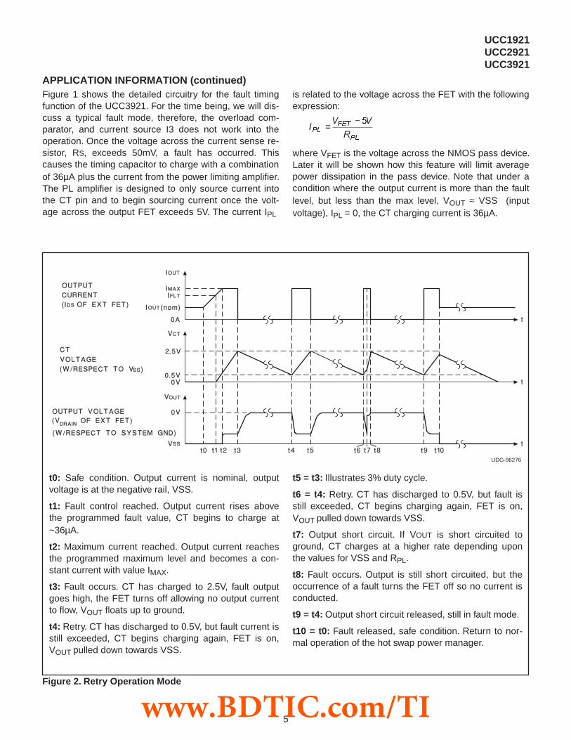
Figure 2. Retry Operation Mode
UDG-96276
t0: Safe condition. Output current is nominal, outputvoltage is at the negative rail, VSS.
t1: Fault control reached. Output current rises abovethe programmed fault value, CT begins to charge at~36µA.
t2: Maximum current reached. Output current reachesthe programmed maximum level and becomes a con-stant current with value IMAX.
t3: Fault occurs. CT has charged to 2.5V, fault outputgoes high, the FET turns off allowing no output currentto flow, VOUT floats up to ground.
t4: Retry. CT has discharged to 0.5V, but fault current isstill exceeded, CT begins charging again, FET is on,VOUT pulled down towards VSS.
t5 = t3: Illustrates 3% duty cycle.
t6 = t4: Retry. CT has discharged to 0.5V, but fault isstill exceeded, CT begins charging again, FET is on,VOUT pulled down towards VSS.
t7: Output short circuit. If VOUT is short circuited toground, CT charges at a higher rate depending uponthe values for VSS and RPL.
t8: Fault occurs. Output is still short circuited, but theoccurrence of a fault turns the FET off so no current isconducted.
t9 = t4: Output short circuit released, still in fault mode.
t10 = t0: Fault released, safe condition. Return to nor-mal operation of the hot swap power manager.
APPLICATION INFORMATION (continued)Figure 1 shows the detailed circuitry for the fault timingfunction of the UCC3921. For the time being, we will dis-cuss a typical fault mode, therefore, the overload com-parator, and current source I3 does not work into theoperation. Once the voltage across the current sense re-sistor, RS, exceeds 50mV, a fault has occurred. Thiscauses the timing capacitor to charge with a combinationof 36µA plus the current from the power limiting amplifier.The PL amplifier is designed to only source current intothe CT pin and to begin sourcing current once the volt-age across the output FET exceeds 5V. The current IPL
is related to the voltage across the FET with the followingexpression:
IV V
RPL
FET
PL
=− 5
where VFET is the voltage across the NMOS pass device.Later it will be shown how this feature will limit averagepower dissipation in the pass device. Note that under acondition where the output current is more than the faultlevel, but less than the max level, VOUT ≈ VSS (inputvoltage), IPL = 0, the CT charging current is 36µA.
www.BDTIC.com/TI
6
UCC1921UCC2921UCC3921
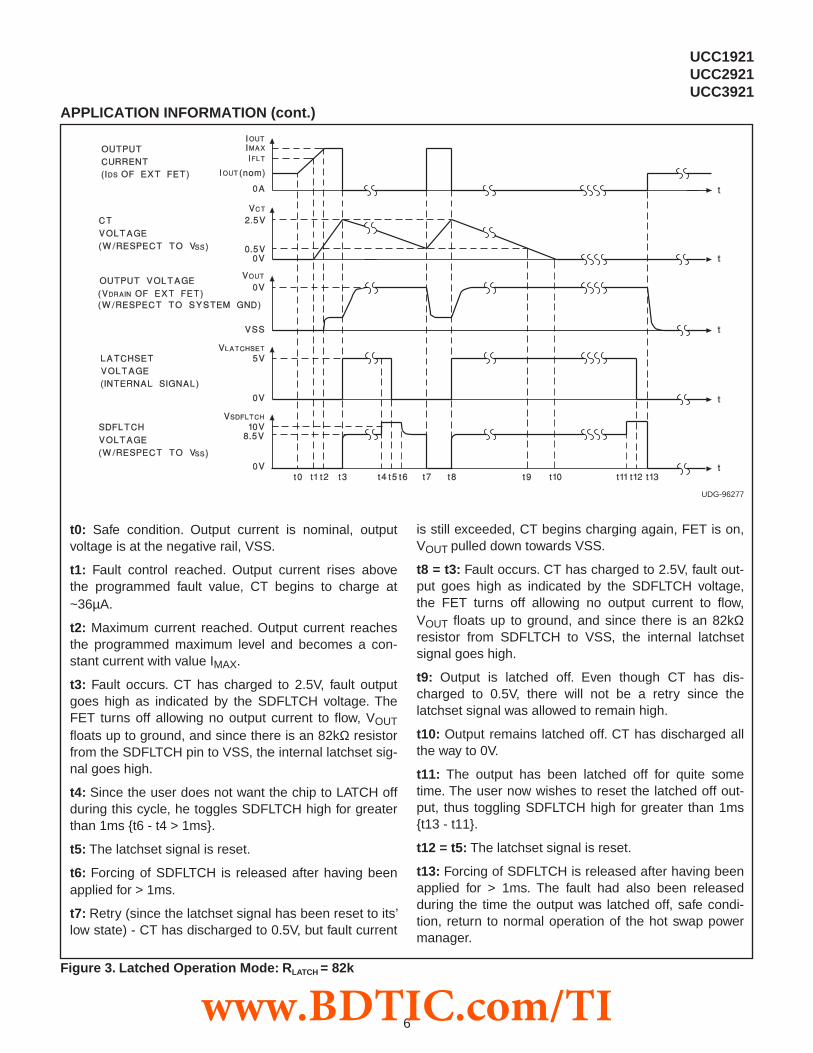
Figure 3. Latched Operation Mode: R LATCH = 82k
APPLICATION INFORMATION (cont.)
UDG-96277
t0: Safe condition. Output current is nominal, outputvoltage is at the negative rail, VSS.
t1: Fault control reached. Output current rises abovethe programmed fault value, CT begins to charge at~36µA.
t2: Maximum current reached. Output current reachesthe programmed maximum level and becomes a con-stant current with value IMAX.
t3: Fault occurs. CT has charged to 2.5V, fault outputgoes high as indicated by the SDFLTCH voltage. TheFET turns off allowing no output current to flow, VOUTfloats up to ground, and since there is an 82kΩ resistorfrom the SDFLTCH pin to VSS, the internal latchset sig-nal goes high.
t4: Since the user does not want the chip to LATCH offduring this cycle, he toggles SDFLTCH high for greaterthan 1ms t6 - t4 > 1ms.
t5: The latchset signal is reset.
t6: Forcing of SDFLTCH is released after having beenapplied for > 1ms.
t7: Retry (since the latchset signal has been reset to its’low state) - CT has discharged to 0.5V, but fault current
is still exceeded, CT begins charging again, FET is on,VOUT pulled down towards VSS.
t8 = t3: Fault occurs. CT has charged to 2.5V, fault out-put goes high as indicated by the SDFLTCH voltage,the FET turns off allowing no output current to flow,VOUT floats up to ground, and since there is an 82kΩresistor from SDFLTCH to VSS, the internal latchsetsignal goes high.
t9: Output is latched off. Even though CT has dis-charged to 0.5V, there will not be a retry since thelatchset signal was allowed to remain high.
t10: Output remains latched off. CT has discharged allthe way to 0V.
t11: The output has been latched off for quite sometime. The user now wishes to reset the latched off out-put, thus toggling SDFLTCH high for greater than 1mst13 - t11.
t12 = t5: The latchset signal is reset.
t13: Forcing of SDFLTCH is released after having beenapplied for > 1ms. The fault had also been releasedduring the time the output was latched off, safe condi-tion, return to normal operation of the hot swap powermanager.
www.BDTIC.com/TI

7
UCC1921UCC2921UCC3921
During a fault, CT will charge at a rate determined by theinternal charging current and the external timing capaci-tor. Once CT charges to 2.5V, the fault comparatorswitches and sets the fault latch. Setting of the fault latchcauses both the output to switch off and the chargingswitch to open. CT must now discharge with the 1µA cur-rent source, I2, until 0.5V is reached. Once the voltage atCT reaches 0.5V, the fault latch resets, which re-enablesthe output and allows the fault circuitry to regain controlof the charging switch. If a fault is still present, the faultcomparator will close the charging switch causing the cy-cle to repeat. Under a constant fault, the duty cycle isgiven by:
Duty CycleA
I APL
=+1
36
µµ
Average power dissipation in the pass element is givenby:
P V IA
I AFET FET MAX
PLAVG
= • •+1
36
µµ
Where VFET>>5V IPL can be approximated as:
V
R
FET
PL
and where IPL>>36µA, the duty cycle can be approxi-mated as :
1µA R
V
PL
FET
•
Therefore, the maximum average power dissipation inthe MOSFET can be approximated by:
P V IA R
V
IMAX A R
FET FET MAX
PL
FET
PL
AVG= • •
•
= • •
1
1
µ
µ
Notice that in the approximation, VFET cancels, therebylimiting the average power dissipation in the NMOS passelement.
Overload Comparator
The linear amplifier in the UCC3921 ensures that theoutput NMOS does not pass more than IMAX (which isVIMAX/RSENSE). In the event the output current exceedsthe programmed IMAX by 0.2V/RSENSE, which can onlyoccur if the output FET is not responding to a commandfrom the IC, CT will begin charging with I3, 1mA, andcontinue to charge to approximately 8V. This allows aconstant fault to show up on the SDFLTCH pin, and alsosince the voltage on CT will continue charging past 2.5Vin an overload fault mode, it can be used for detection of
output FET failure or to build redundancy into the sys-tem.
Determining External Component Values
To set RVDD (see Fig. 4) the following must be achieved:
V
R
V
R RmAIN
VDD
min>
++10
1 22
In order to estimate the minimum timing capacitor, CT,several things must be taken into account. For example,given the schematic in Figure 4 as a possible (and at thispoint, a standard) application, certain external compo-nent values must be known in order to estimate CTMIN.Now, given the values of COUT, Load, RSENSE, VSS, andthe resistors determining the voltage on the IMAX pin,the user can calculate the approximate startup time ofthe node VOUT. This startup time must be faster than thetime it takes for CT to charge to 2.5V (relative to VSS),and is the basis for estimating the minimum value of CT.In order to determine the value of the sense resistor,RSENSE, assuming the user has determined the fault cur-rent, RSENSE can be calculated by:
RmV
ISENSE
FAULT
= 50
Next, the variable IMAX must be calculated. IMAX is themaximum current that the UCC3921 will allow throughthe transistor, M1, and it can be shown that duringstartup with an output capacitor the power MOSFET, M1,can be modeled as a constant current source of valueIMAX where
IV
RMAX
IMAX
SENSE
= where VIMAX = voltage on pin IMAX.
Given this information, calculation of the startup time isnow possible via the following:
APPLICATION INFORMATION (continued)
Figure 4.
UDG-96278
www.BDTIC.com/TI

8
UCC1921UCC2921UCC3921
Current Source Load:
TC V
I ISTART
OUT SS
MAX LOAD
=•
−
Resistive Load:
T
C R nI R
I R V
START
OUT OUT
MAX OUT
MAX OUT SS
=
• ••
• −
l
Once TSTART is calculated, the power limit feature of theUCC3921 must be addressed and component values de-rived. Assuming the user chooses to limit the maximum
allowable average power that will be associated with thehot swap power manager, the power limiting resistor,RPL, can be easily determined by the following:
RP avg
A IPL
FET
MAX
=•1µ
where a minimum RPL exists
defined by RV
mAPL
SSmin =
5(Refer to Figure 5).
Finally, after computing the aforementioned variables, theminimum timing capacitor can be derived as such:
Current Source Load:
( )C
T A R V V
R
T
START PL SS
PL
min =
• • • + −
•
3 72 10
10
µ
Resistive Load:
( )C
T A R V V I R
R
R
T
START PL SS MAX OUT
PL
O
min =
• • • + − − •
•
+•
3 36 5
5
3
µ
UT SS OUT
PL
V C
R
• ••5
Level Shift Circuitry to Interface with SDFLTCH
Some type of circuit is needed to interface with theUCC3921 via SDFLTCH, such as opto-couplers or levelshift circuitry. Figure 6 depicts one implementation oflevel shift circuitry that could be used, showing compo-nent values selected for a typical –48V telecommunica-tions application. There are three communicationconditions which could occur; two of which are Hot SwapPower Manager (HSPM) state output indications, and thethird being an External Shutdown.
1) When open, and under a non-fault condition,SDFLTCH is pulled to a low state. In Figure 6, the N-channel level shift transistor is off, and theFAULT OUT signal is pulled to LOCAL VDD throughR3. This indicates that the HSPM is not faulted.
2) When a fault is detected by the fault timer or under-voltage lockout, this pin will drive to a high state, indi-cating that the external power FET is off. In Figure 6,the N-channel level shift transistor will conduct, andthe FAULT OUT signal will be pulled to a Schottky Di-ode voltage drop below LOCAL GND. This indicatesthat the HSPM is faulted. The Schottky Diode is nec-essary to ensure that the FAULT OUT signal doesnot traverse too far below LOCAL GND, making faultdetection difficult.
APPLICATION INFORMATION (continued)
25
22.5
20
17.5
15
12.5
10
7.5
5
2.5
00 25 50 75 100 125 150 175 200
VFET
R
R
PL
PL
= 500k
= 200k
RPL = 1M
RPL = 2M
RPL = 5M
RPL = 10M
RPL= ∞I = 4AMAX
= ∞
Figure 5. Plot Average Power vs FET Voltage forIncreasing Values of R PL
Figure 6. Possible Level Shift Circuitry toInterface to the UCC3921, showing componentvalues selected for a typical telecom application.
UDG-96279
= ∞
www.BDTIC.com/TI

9
UCC1921UCC2921UCC3921
If a 5k < RLATCH < 250kΩ resistor is tied betweenSDFLTCH & VSS, as optionally shown in Figure 6,then the latched operating mode (described earlier)will be invoked upon the occurrence of a fault.
3) To externally shutdown the HSPM, the SHUTDOWNsignal (typically held at LOCAL VDD) must be pulledto LOCAL GND. Assuming SHUTDOWN is tied toLOCAL GND, the P-channel level shift transistor willconduct, driving SDFLTCH high (to roughly VDD plusa diode). By sourcing > 250µA into SDFLTCH for >1ms the output to the external power FET will be dis-abled. The current sourced into SDFLTCH must be
limited to 10mA or less: ISDFLTCHMAX < 10mA.
SAFETY RECOMMENDATIONS
Although the UCC3921 is designed to provide systemprotection for all fault conditions, all integrated circuitscan ultimately fail short. For this reason, if the UCC3921is intended for use in safety critical applications whereUL or some other safety rating is required, a redundantsafety device such as a fuse should be placed in serieswith the external power FET. The UCC3921 will preventthe fuse from blowing for virtually all fault conditions, in-creasing system reliability and reducing maintenancecost, in addition to providing the hot swap benefits of thedevice.
APPLICATION INFORMATION (continued)
Ω
Figure 7. Typical Telecommuications Application
(The “Negative Magnitude-Side” of the Supply is Switched in)
UDG-98053
www.BDTIC.com/TI
10
UCC1921UCC2921UCC3921
UNITRODE CORPORATION7 CONTINENTAL BLVD. • MERRIMACK, NH 03054TEL. (603) 424-2410 • FAX (603) 424-3460
Ω
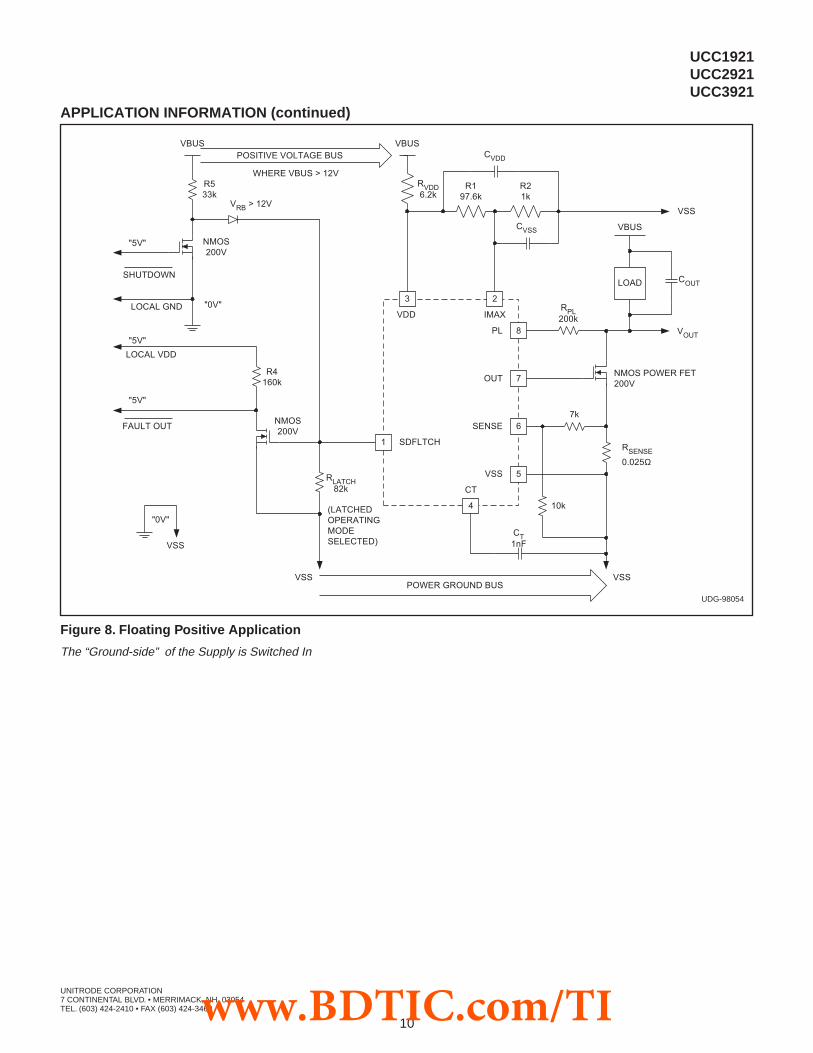
Figure 8. Floating Positive Application
The “Ground-side” of the Supply is Switched In
APPLICATION INFORMATION (continued)
UDG-98054
www.BDTIC.com/TI

PACKAGING INFORMATION
Orderable Device Status (1) PackageType
PackageDrawing
Pins PackageQty
Eco Plan (2) Lead/Ball Finish MSL Peak Temp (3)
UCC2921D ACTIVE SOIC D 8 75 Green (RoHS &no Sb/Br)
CU NIPDAU Level-2-260C-1 YEAR
UCC2921DG4 ACTIVE SOIC D 8 75 Green (RoHS &no Sb/Br)
CU NIPDAU Level-2-260C-1 YEAR
UCC2921DTR ACTIVE SOIC D 8 2500 Green (RoHS &no Sb/Br)
CU NIPDAU Level-2-260C-1 YEAR
UCC2921DTRG4 ACTIVE SOIC D 8 2500 Green (RoHS &no Sb/Br)
CU NIPDAU Level-2-260C-1 YEAR
UCC3921D ACTIVE SOIC D 8 75 Green (RoHS &no Sb/Br)
CU NIPDAU Level-1-260C-UNLIM
UCC3921D/81143 ACTIVE SOIC D 8 75 Green (RoHS &no Sb/Br)
CU NIPDAU Level-2-260C-1 YEAR
UCC3921D/81143G4 ACTIVE SOIC D 8 75 Green (RoHS &no Sb/Br)
CU NIPDAU Level-2-260C-1 YEAR
UCC3921DG4 ACTIVE SOIC D 8 75 Green (RoHS &no Sb/Br)
CU NIPDAU Level-1-260C-UNLIM
UCC3921DTR ACTIVE SOIC D 8 2500 Green (RoHS &no Sb/Br)
CU NIPDAU Level-1-260C-UNLIM
UCC3921DTR/81143 ACTIVE SOIC D 8 2500 Green (RoHS &no Sb/Br)
CU NIPDAU Level-2-260C-1 YEAR
UCC3921DTR/81143G4 ACTIVE SOIC D 8 2500 Green (RoHS &no Sb/Br)
CU NIPDAU Level-2-260C-1 YEAR
UCC3921DTRG4 ACTIVE SOIC D 8 2500 Green (RoHS &no Sb/Br)
CU NIPDAU Level-1-260C-UNLIM
UCC3921N ACTIVE PDIP P 8 50 Green (RoHS &no Sb/Br)
CU NIPDAU N / A for Pkg Type
UCC3921NG4 ACTIVE PDIP P 8 50 Green (RoHS &no Sb/Br)
CU NIPDAU N / A for Pkg Type
(1) The marketing status values are defined as follows:ACTIVE: Product device recommended for new designs.LIFEBUY: TI has announced that the device will be discontinued, and a lifetime-buy period is in effect.NRND: Not recommended for new designs. Device is in production to support existing customers, but TI does not recommend using this part ina new design.PREVIEW: Device has been announced but is not in production. Samples may or may not be available.OBSOLETE: TI has discontinued the production of the device.
(2) Eco Plan - The planned eco-friendly classification: Pb-Free (RoHS), Pb-Free (RoHS Exempt), or Green (RoHS & no Sb/Br) - please checkhttp://www.ti.com/productcontent for the latest availability information and additional product content details.TBD: The Pb-Free/Green conversion plan has not been defined.Pb-Free (RoHS): TI's terms "Lead-Free" or "Pb-Free" mean semiconductor products that are compatible with the current RoHS requirementsfor all 6 substances, including the requirement that lead not exceed 0.1% by weight in homogeneous materials. Where designed to be solderedat high temperatures, TI Pb-Free products are suitable for use in specified lead-free processes.Pb-Free (RoHS Exempt): This component has a RoHS exemption for either 1) lead-based flip-chip solder bumps used between the die andpackage, or 2) lead-based die adhesive used between the die and leadframe. The component is otherwise considered Pb-Free (RoHScompatible) as defined above.Green (RoHS & no Sb/Br): TI defines "Green" to mean Pb-Free (RoHS compatible), and free of Bromine (Br) and Antimony (Sb) based flameretardants (Br or Sb do not exceed 0.1% by weight in homogeneous material)
(3) MSL, Peak Temp. -- The Moisture Sensitivity Level rating according to the JEDEC industry standard classifications, and peak soldertemperature.
Important Information and Disclaimer:The information provided on this page represents TI's knowledge and belief as of the date that it is
PACKAGE OPTION ADDENDUM
www.ti.com 18-Sep-2008
Addendum-Page 1
www.BDTIC.com/TI
provided. TI bases its knowledge and belief on information provided by third parties, and makes no representation or warranty as to theaccuracy of such information. Efforts are underway to better integrate information from third parties. TI has taken and continues to takereasonable steps to provide representative and accurate information but may not have conducted destructive testing or chemical analysis onincoming materials and chemicals. TI and TI suppliers consider certain information to be proprietary, and thus CAS numbers and other limitedinformation may not be available for release.
In no event shall TI's liability arising out of such information exceed the total purchase price of the TI part(s) at issue in this document sold by TIto Customer on an annual basis.
PACKAGE OPTION ADDENDUM
www.ti.com 18-Sep-2008
Addendum-Page 2
www.BDTIC.com/TI
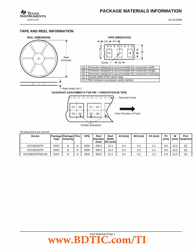
TAPE AND REEL INFORMATION
*All dimensions are nominal
Device PackageType
PackageDrawing
Pins SPQ ReelDiameter
(mm)
ReelWidth
W1 (mm)
A0 (mm) B0 (mm) K0 (mm) P1(mm)
W(mm)
Pin1Quadrant
UCC2921DTR SOIC D 8 2500 330.0 12.4 6.4 5.2 2.1 8.0 12.0 Q1
UCC3921DTR SOIC D 8 2500 330.0 12.4 6.4 5.2 2.1 8.0 12.0 Q1
UCC3921DTR/81143 SOIC D 8 2500 330.0 12.4 6.4 5.2 2.1 8.0 12.0 Q1
PACKAGE MATERIALS INFORMATION
www.ti.com 29-Jul-2008
Pack Materials-Page 1
www.BDTIC.com/TI

*All dimensions are nominal
Device Package Type Package Drawing Pins SPQ Length (mm) Width (mm) Height (mm)
UCC2921DTR SOIC D 8 2500 346.0 346.0 29.0
UCC3921DTR SOIC D 8 2500 346.0 346.0 29.0
UCC3921DTR/81143 SOIC D 8 2500 346.0 346.0 29.0
PACKAGE MATERIALS INFORMATION
www.ti.com 29-Jul-2008
Pack Materials-Page 2
www.BDTIC.com/TI

www.BDTIC.com/TI
www.BDTIC.com/TI

www.BDTIC.com/TI

IMPORTANT NOTICE
Texas Instruments Incorporated and its subsidiaries (TI) reserve the right to make corrections, modifications, enhancements, improvements,and other changes to its products and services at any time and to discontinue any product or service without notice. Customers shouldobtain the latest relevant information before placing orders and should verify that such information is current and complete. All products aresold subject to TI’s terms and conditions of sale supplied at the time of order acknowledgment.
TI warrants performance of its hardware products to the specifications applicable at the time of sale in accordance with TI’s standardwarranty. Testing and other quality control techniques are used to the extent TI deems necessary to support this warranty. Except wheremandated by government requirements, testing of all parameters of each product is not necessarily performed.
TI assumes no liability for applications assistance or customer product design. Customers are responsible for their products andapplications using TI components. To minimize the risks associated with customer products and applications, customers should provideadequate design and operating safeguards.
TI does not warrant or represent that any license, either express or implied, is granted under any TI patent right, copyright, mask work right,or other TI intellectual property right relating to any combination, machine, or process in which TI products or services are used. Informationpublished by TI regarding third-party products or services does not constitute a license from TI to use such products or services or awarranty or endorsement thereof. Use of such information may require a license from a third party under the patents or other intellectualproperty of the third party, or a license from TI under the patents or other intellectual property of TI.
Reproduction of TI information in TI data books or data sheets is permissible only if reproduction is without alteration and is accompaniedby all associated warranties, conditions, limitations, and notices. Reproduction of this information with alteration is an unfair and deceptivebusiness practice. TI is not responsible or liable for such altered documentation. Information of third parties may be subject to additionalrestrictions.
Resale of TI products or services with statements different from or beyond the parameters stated by TI for that product or service voids allexpress and any implied warranties for the associated TI product or service and is an unfair and deceptive business practice. TI is notresponsible or liable for any such statements.
TI products are not authorized for use in safety-critical applications (such as life support) where a failure of the TI product would reasonablybe expected to cause severe personal injury or death, unless officers of the parties have executed an agreement specifically governingsuch use. Buyers represent that they have all necessary expertise in the safety and regulatory ramifications of their applications, andacknowledge and agree that they are solely responsible for all legal, regulatory and safety-related requirements concerning their productsand any use of TI products in such safety-critical applications, notwithstanding any applications-related information or support that may beprovided by TI. Further, Buyers must fully indemnify TI and its representatives against any damages arising out of the use of TI products insuch safety-critical applications.
TI products are neither designed nor intended for use in military/aerospace applications or environments unless the TI products arespecifically designated by TI as military-grade or "enhanced plastic." Only products designated by TI as military-grade meet militaryspecifications. Buyers acknowledge and agree that any such use of TI products which TI has not designated as military-grade is solely atthe Buyer's risk, and that they are solely responsible for compliance with all legal and regulatory requirements in connection with such use.
TI products are neither designed nor intended for use in automotive applications or environments unless the specific TI products aredesignated by TI as compliant with ISO/TS 16949 requirements. Buyers acknowledge and agree that, if they use any non-designatedproducts in automotive applications, TI will not be responsible for any failure to meet such requirements.
Following are URLs where you can obtain information on other Texas Instruments products and application solutions:
Products Applications
Amplifiers amplifier.ti.com Audio www.ti.com/audio
Data Converters dataconverter.ti.com Automotive www.ti.com/automotive
DLP® Products www.dlp.com Communications and www.ti.com/communicationsTelecom
DSP dsp.ti.com Computers and www.ti.com/computersPeripherals
Clocks and Timers www.ti.com/clocks Consumer Electronics www.ti.com/consumer-apps
Interface interface.ti.com Energy www.ti.com/energy
Logic logic.ti.com Industrial www.ti.com/industrial
Power Mgmt power.ti.com Medical www.ti.com/medical
Microcontrollers microcontroller.ti.com Security www.ti.com/security
RFID www.ti-rfid.com Space, Avionics & www.ti.com/space-avionics-defenseDefense
RF/IF and ZigBee® Solutions www.ti.com/lprf Video and Imaging www.ti.com/video
Wireless www.ti.com/wireless-apps
Mailing Address: Texas Instruments, Post Office Box 655303, Dallas, Texas 75265Copyright © 2010, Texas Instruments Incorporated
www.BDTIC.com/TI