Embed Size (px)
Citation preview

Electronics and Robotics LLC ootbrobotics.com
Last revision 8/19/2021

2
Electronics and Robotics LLC ootbrobotics.com
Table of Contents ...................................................................................................................................... 2
Overview .................................................................................................................................................... 5
Warning Read Before Continuing .............................................................................................................. 6
Features .................................................................................................................................................... 7
MAX 10 CPLD ....................................................................................................................................... 7
Signal Tap Analyzer Capable ................................................................................................................ 7
I/O and Indicators .................................................................................................................................. 7
USB ....................................................................................................................................................... 7
External Flash Memory .......................................................................................................................... 7
USB Flash Programming ....................................................................................................................... 7
IO Protection .......................................................................................................................................... 8
Electrical Characteristics ........................................................................................................................... 9
USB Programer Overview ....................................................................................................................... 10
USB Driver Installation ............................................................................................................................. 11
Programming the MXDB .......................................................................................................................... 12
Requirements ...................................................................................................................................... 12
Procedure ............................................................................................................................................ 12
Step 1: Launch Quartus ................................................................................................................... 12
Step 2: Connect the Programmer to the MXDB ............................................................................... 13
Figure 1: JTAG Cable Orientation ............................................................................................ 13
Step 3: Power the MXDB and USB Programmer. ............................................................................ 13
Step 4: Open the Programmer Window in Quartus .......................................................................... 13
Step 6: Hardware Setup .................................................................................................................. 14
Step 6.1 Hardware Setup ................................................................................................................ 15
Step 6.2 Hardware Setup Cont. ....................................................................................................... 15
Step 7: Add File ............................................................................................................................... 15

3
Electronics and Robotics LLC ootbrobotics.com
Step 8: Tristate unused pins ............................................................................................................ 16
Step 9: Programming the MXDB with a SOF/POF File .................................................................... 16
Appendix I: Pin Allocations ...................................................................................................................... 18
General Overview of BGA Pin Designators ......................................................................................... 18
Figure 2: MAX 10 UBGA 169 footprint proveded by Intel (Bottom View) ................................. 18
Breadboard Connections ..................................................................................................................... 19
Figure 3:Breadboard Connections ........................................................................................... 19
General Purpose LEDs ........................................................................................................................ 20
Figure 4: GPIO LEDs and respective pins ............................................................................... 20
Clocks .................................................................................................................................................. 20
Figure 5: MXDB available clock sources ................................................................................. 20
Seven Segment Displays ..................................................................................................................... 21
Figure 6:Seven segment displays ............................................................................................ 21
Figure 7:Display LED Labels ................................................................................................... 21
Figure 8:Display LED assignments .......................................................................................... 21
USB Pin Assignments .......................................................................................................................... 22
Figure 9:USB pin assignments ................................................................................................ 22
Flash Memory Pin Assignments .......................................................................................................... 23
Figure 10: Flash memory pin assignments .............................................................................. 23
Appendix II: Flash Programmer GUI ........................................................................................................ 24
Perquisites ........................................................................................................................................... 24
Using the Flash Programmer GUI Interface ......................................................................................... 25
Figure 11: Flash Programmer GUI Window ............................................................................. 25
Device Connection ........................................................................................................................... 25
Writing to Flash ................................................................................................................................ 25
Reading from Flash ......................................................................................................................... 26
Appendix III: Configuring FTDI Clock ....................................................................................................... 27
FTDI Clock Configure Procedure ......................................................................................................... 27
Restore the Default FTDI Configuration ............................................................................................... 29
Appendix IV: Troubleshooting .................................................................................................................. 30
4
Electronics and Robotics LLC ootbrobotics.com
What if the programmer is not visible despite being connected? ......................................................... 31

5
Electronics and Robotics LLC ootbrobotics.com
The MXDB is Out of the Box’s 2nd generation programmable logic development platform. The MXDB is a
platform designed specifically for learning the basics of digital electronics from the lowest level of logic
gates to microprocessors. The board features a USB FIFO bridge, external flash memory and
accompaniment software to program data to the flash memory with a PC. The board’s form-factor also
makes it ideal for interfacing with a solderless breadboard.

6
Electronics and Robotics LLC ootbrobotics.com
The MXDB is a FPGA platform that also contains additional ICs capable of driving signals to the FPGA
controlled via read strobe pins. There is a jumper J5 that when left open will help prevent inadvertent IO
conflicts, but this should not be considered a complete solution! It is the user’s responsibility to review the
device schematic and the FPGA pin planner assignments before uploading any design to the device.

7
Electronics and Robotics LLC ootbrobotics.com
The MXDB is by default configured with a MAX 10 2K logic element FPGA. Unlike most FPGAs the MAX
10 family of devices has built in non-volatile memory allowing the device to function like a CPLD. This
means that the program on the device can remain when the device is powered down. The device will
simply resume operation upon being powered again.
The MXDB can use the Out of the Box USB Programmer to run the Signal Tap Logic Analyzer.
The MXDB has 34 GPIO pins 2 of which are optionally used as global clock inputs. There are also 4
general purpose LEDs, 2 seven segment LED displays, and a single power LED.
The MXDB is equipped with a FT-240X USB to FIFO bridge that allows the FPGA to send and receive data
from a PC USB connection. The Out of the Box Flash Programmer GUI uses this interface for flash
programming.
The MXDB features parallel flash memory connected to the FPGA. This ROM could be used for look up
tables, soft processor program memory etc.
As mentioned above the Out of the Box Flash Programmer GUI interfaces with the MXDB’s USB
connection to program and read from the on-board flash memory.

8
Electronics and Robotics LLC ootbrobotics.com
The MXDB has a jumper J5 used to connect or disconnect the read strobe signals to the USB to FIFO
device and the parallel flash. With this jumper open the read strobes will be pulled false. This jumper is
used to help prevent bus conflicts if an inexperienced user accidently assigns a design pin to a strobe
erroneously. Doing so could allow the flash or USB devices to drive pins to the FPGA. Note: to utilize the
flash Programmer GUI this jumper must be present.

9
Electronics and Robotics LLC ootbrobotics.com
Electrical Characteristics
Item Min Nominal Max Unit
Un-programmed Current draw < 20 mA
3.3V current output12 ~7002 15002 mA
GPIO VIH
3.6 V
GPIO VIL -0.3 0.8 V
1) This includes the current required to power the board itself
2) The current output is likely limited by efficiency of the regulator and maximum current of USB 2.0
(500mA). The 3.3V regulator is rated for 1.5A output.

10
Electronics and Robotics LLC ootbrobotics.com
The Out of the Box CPLD/FPGA Programmer is a low-cost alternative to the Altera ByteBlaster II as well as
the Terasic variant. The Out of the Box USB Programmer will only work with 3.3V devices and is intended
to pair specifically with the Out of the Box Development Boards.
The programmer contains very little hardware. The programmer consists only of an FT2232H USB IC and
its supporting components. This FTDI device contains a JTAG peripheral which is used for programming
and generally interfacing with the CPLD/FPGA.

11
Electronics and Robotics LLC ootbrobotics.com
Before The MXDB and Out of the Box USB Programmer can be used their USB drivers must be installed.
The USB programmer and MXDB both use FTDI USB devices. Install the latest FTDI drivers from
https://ftdichip.com/drivers/d2xx-drivers/. download the setup executable found in the comments section.
Provided with this document is a batch (.bat) file and support files for automatically installing the required
Quartus driver for the Out of the Box Programmer.
The Automated install currently supports version 19.1 of Quartus.
1) Double click on OOTB_Programmer_install.bat and a prompt asking for admin privileges will
display.
2) When asked to allow this app to make changes to your computer, select yes. This is required
since the install directory of Quartus is in a protected section of the C: drive.
3) If successful, the following will be displayed
Otherwise Quartus is not installed or in the default directory.
Provided with this document is a driver for interfacing the CPLD/FPGA programmer directly with Quartus
). Place this file in the appropriate Quartus directory structure such
as below example.
C:\intelFPGA_lite\19.1\quartus\bin64
The base directory will be whatever was specified at the time of the Quartus install. The C drive is the
default location.

12
Electronics and Robotics LLC ootbrobotics.com
The MXDB more specifically the MAX 10 (10M02SCU169C8G) can be programmed with any Intel
compatible JTAG programmer. This tutorial will use the Out of the Box USB Programmer, but other
devices such as the Terasic USB Blaster Cable can be used as well.
• Intel compatible USB blaster.
o This tutorial will use the Out of the Box CPLD Programmer
• MXDB
o Including USB cable for connecting the board to the computer.
• Quartus 19.1
Use the following steps to program the MXDB
Open Quartus 19.1 or “Programmer (Quartus Prime 19.1)”

13
Electronics and Robotics LLC ootbrobotics.com
Connect the 10-pin JTAG cable between the programmer and the MXDB. The JTAG cable can be oriented
with either end going to the MXDB or USB Programmer as long as the ribbon points away from the boards
as shown below. To correspond the red stripe to pin 1 of each board orient as shown below.
Figure 3: JTAG Cable Orientation
Use standard USB cables (USB A to USB B) to connect both the MXDB and USB Programmer to the
computer. The MXDB cannot be programmed without being powered over USB.
If using Quartus and not just the programmer app, the Programmer window is launched via the button in
Quartus’ top pane.
Figure 1: Programmer JTAG Connection Figure 2: MXDB JTAG Connection

14
Electronics and Robotics LLC ootbrobotics.com
When the Programmer Window is opened check to see if the hardware has been recognized. Reference
the highlighted portion of the following image to find out what hardware is connected.
If the Programmer Window does not display “No Hardware” and instead lists “ ”
(be advised a portion of this text could be cut off due to the size of the dialog x.x corresponds to the version
number) proceed to Step 7. If the window does display “No Hardware” proceed to Step 6.1.

15
Electronics and Robotics LLC ootbrobotics.com
Press to tell Quartus what tool to select. Doing so will open the following window shown
below.
If the device “ ” is displayed as above proceed to Step 6.3. Otherwise, follow this
tutorial.
Double click “ ” (x.x denotes the version number) to select the programmer. (This is
the device name in Quartus for the Out of the Box CPLD Programmer). Then exit the Hardware Setup
Window. After a small delay the Programmer Window should display the selected device name next to
.
In this step select a file to be programmed to the MXDB. To do this use the button in the
Quartus Programmer Window.
Note:
Both SOF and POF files can be used. SOF files are volatile meaning they are erased once the
MXDB is powered down. POF files are non-volatile. These contents will remain on the device until
erased.
Upon adding a file ensure that the device is “10M02SCU169C8G” this is the device installed upon the
MXDB.

16
Electronics and Robotics LLC ootbrobotics.com
For SOF files the only option when programming is Program/Configure
POF programming has the following options
Verify - Ensures that the data in the device is the same as the programming file.
Blank Check- Ensures that a device was successfully erased
Erase - Erases the contents of the device.
It is always recommended to tristate unused i/o pins on the MXDB. To do this go to the assignments tab in
Quartus.
Select Device followed by from the popup window.
Set Reserve all unused pins: to “As input tri-stated”
Once an appropriate file has been selected for the MXDB press the button in the programmer
window to begin programming. Be advised that POF files will take a fair amount of time to program. SOF
files will program much faster.
The progress of the device programming will be displayed by a bar graph. Upon successful completion the
display should read . If there is a result of Try the following
• Ensure that the JTAG connection of the programmer is indeed connected to the MXDB.

17
Electronics and Robotics LLC ootbrobotics.com
• Try selecting the option of just “Erase” first then program. If this works, try programming again.
o If not, disconnect the MXDB from power and from the JTAG cable for 30 seconds. Then
plug everything back in and attempt an erase again.

18
Electronics and Robotics LLC ootbrobotics.com
The MXDB MAX 10 FPGA comes in a BGA (Ball Grid Array) footprint. BGA pins have an alpha numeric
designation since BGA chips organize their pins in both rows and columns as shown in the footprint
diagram below.
Figure 4: MAX 10 UBGA 169 footprint proveded by Intel (Bottom View)
When programming the MAX 10 FPGA with Quartus, the pin assignments will be alpha numeric; row letter
followed by column number.
19
Electronics and Robotics LLC ootbrobotics.com
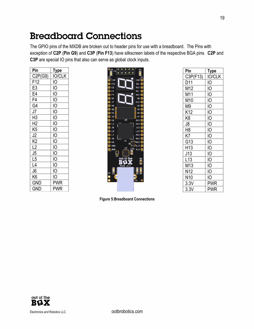
The GPIO pins of the MXDB are broken out to header pins for use with a breadboard. The Pins with
exception of C2P (Pin G9) and C3P (Pin F13) have silkscreen labels of the respective BGA pins. C2P and
C3P are special IO pins that also can serve as global clock inputs.
Figure 5:Breadboard Connections
Pin Type
C2P(G9) IO/CLK
F12 IO
E3 IO
E4 IO
F4 IO
G4 IO
J7 IO
H3 IO
H2 IO
K5 IO
J2 IO
K2 IO
L2 IO
J5 IO
L5 IO
L4 IO
J6 IO
K6 IO
GND PWR
GND PWR
Pin Type
C3P(F13) IO/CLK
D11 IO
M12 IO
M11 IO
M10 IO
M9 IO
K12 IO
K8 IO
J8 IO
H8 IO
K7 IO
G13 IO
H13 IO
J13 IO
L13 IO
M13 IO
N12 IO
N10 IO
3.3V PWR
3.3V PWR

20
Electronics and Robotics LLC ootbrobotics.com
The MXDB has 4 General purpose LEDs.
LED Reference Designator FPGA Pin Comment D3 L12 Intended as a general status
LED
D4 E10 Intended as a general status LED
D51 N11 Intended as a general status LED. Also intended to indicate USB bytes received.
D61 K13 Intended as a general status LED. Also intended to indicate USB bytes transmitted.
Figure 6: GPIO LEDs and respective pins
1)These LEDs are intended to be used for USB data transmission indicators during flash programming
The MXDB’s FPGA has many dedicated clock pins. 4 of the available clock pins are available, or which 2
do not already have an on-board clock attached to them.
Clock FPGA Pin Source Schematic label
CLK0p H6 FTDI USB IC (6MHz default) configurable
FT_CLK
CLK1p H4 On-board oscillator (4MHz)
EXTCLK
CLK2p G9 N/A Breadboard connection
CLK2p
CLK3p F13 N/A Breadboard connection
CLK3p
Figure 7: MXDB available clock sources
Although not available on the MXDB, the MAX 10 FPGA supports differential clock inputs which can be
used to trigger events on rising and falling clock edges. This differential capability is the reason behind the
CLKxy naming convention. X represents the clock pin number. Y in the example denotes the differential
signal polarity (p for positive and n for negative).

21
Electronics and Robotics LLC ootbrobotics.com
The MXDB has two seven segment LED displays highlighted below. The left display is U8 and right is U7.
Figure 8:Seven segment displays
The display segment names are shown in the next figure
Figure 9:Display LED Labels
Segment Signal (U8 Left)
FPGA Pin Segment Signal (U7 Right)
FPGA Pin
A H10 A D9
B F8 B C9
C E8 C G12
D J12 D L10
E H9 E K10
F J10 F J9
G L11 G E6
DP E9 DP E12 Figure 10:Display LED assignments

22
Electronics and Robotics LLC ootbrobotics.com
The FT-240x device is a parallel interface USB device. The pin assignments for the Device are as follows.
FPGA PIN Function Description
N7 USB DATA0 Data Bus pin
N5 USB DATA1 Data Bus pin
N6 USB DATA2 Data Bus pin
M2 USB DATA3 Data Bus pin
M7 USB DATA4 Data Bus pin
M4 USB DATA5 Data Bus pin
N4 USB DATA6 Data Bus pin
M5 USB DATA7 Data Bus pin
M8 USB RXF̅̅ ̅̅ ̅ Low true indication of RX data available
N9 USB TXE Low true indication of TX function ready to receive data
J1 USB RD Low true USB RX buffer read strobe
K1 USB WR Low true USB TX buffer write strobe
M1 SI/WU Low true Send Immediate strobe. Also used to wake up device from sleep
N8 PWREN(FT-240 CBUS6 pin) Output is low after device is ready
H6 FT_CLK (FT-240 CBUS5 pin configured as CLK6MHz)
6MHz oscillator output can be used as a global clock to the FPGA
Figure 11:USB pin assignments

23
Electronics and Robotics LLC ootbrobotics.com
The MXDB pin assignments for the on-board parallel flash memory are as follows
FPGA PIN Function Description
C13 A0 Flash address pin
D12 A1 Flash address pin
C11 A2 Flash address pin
C12 A3 Flash address pin
F1 A4 Flash address pin
E1 A5 Flash address pin
D1 A6 Flash address pin
C1 A7 Flash address pin
B5 A8 Flash address pin
A5 A9 Flash address pin
A7 A10 Flash address pin
B6 A11 Flash address pin
B1 A12 Flash address pin
A4 A13 Flash address pin
B4 A14 Flash address pin
C2 A15 Flash address pin
B2 A16 Flash address pin
A3 A17 Flash address pin
A2 A18 Flash address pin
B13 FL IO 0 Flash data pin
B12 FL IO 1 Flash data pin
A12 FL IO 2 Flash data pin
B11 FL IO 3 Flash data pin
A11 FL IO 4 Flash data pin
B10 FL IO 5 Flash data pin
A10 FL IO 6 Flash data pin
A9 FL IO 7 Flash data pin
B3 FL WE Flash Write enable
A6 FL OE Flash Output enable
A8 FL CE Flash Chip enable
Figure 12: Flash memory pin assignments

24
Electronics and Robotics LLC ootbrobotics.com
The Flash Programmer GUI (Graphical User Interface) is a program used to read data from and write data
to the on-board flash of the MXDB.
• Run the FlashProgrammer-installer.exe to install the GUI.
• Before the GUI can be use with the MXDB, the FlashProgrammer POF or SOF files need to be
loaded to the MXDB. These files enable communication with the board via USB to the on-board
flash. Using the SOF version of the programmer is quick, but upon powering down of the board this
program will be erased. If using the POF version of the FlashProgrammer subsequent SOF files will
take precedent in the device, but the POF program will be useable again upon a power cycle of the
device.
o It is advised to use the POF version of the FlashProgrammer file since a power cycle (un-
powering then powering again) will revert the MXDB to being ready to use with the GUI.
• The Jumper location J5 of the board must have a jumper present. This jumper allows for the reading
of data from the USB and Flash devices. The jumper exists to break this connection for new users
whom may accidently assign the data pins of the Flash/USB devices which could result in damage
to the board.

25
Electronics and Robotics LLC ootbrobotics.com
Figure 13: Flash Programmer GUI Window
When a MXDB board is connected to the Flash Programmer GUI the device connection will display a check
mark
When no device is present the device connection will display a spinning wheel.
To write to the MXDB on-board flash memory select the browse button . From the browser window that
pops up, locate a MIF file to load to the flash. Once a file has been selected the Write button will become
clickable.

26
Electronics and Robotics LLC ootbrobotics.com
Once Write is clicked the GUI will begin the Erase, Write, and Verify processes. Each process if successful
will be denoted by a .
If instead a is displayed, then the process has failed. Often the reason for this failure is that the
jumper J5 is not present. Another possibility is that the FPGA is not programmed with either the
FlashProgrammer SOF/POF file required for communication with the GUI.
To read from the MXDB on-board flash memory select the button. In the subsequent browser
window create a file or select a file to load the data into. After making this selection the progress bar will
become active. If this does not happen then the process has failed. Often the reason for this failure is that
the jumper J5 is not present. Another possibility is that the FPGA does not contain the FlashProgrammer
SOF/POF file required for communication with the GUI.

27
Electronics and Robotics LLC ootbrobotics.com
The FTDI USB device on the MXDB by default outputs a 6MHz clock. However, this clock can be
configured to 12MHz or 24MHz as well.
USE CAUTION when reconfiguring an FTDI device. As FTDI states in their download page.
“The use of some of these utilities by an end user may result in a device being rendered useless.”
Only change the parameters mentioned in this guide and always preserve the default config of the device.
1) Download and install FT_Prog from FTDI https://ftdichip.com/utilities/
2) Make sure the Out of the Box USB Programmer is disconnected from the computer.
3) Connect in the MXDB to the computer.
4) Open FT_Prog
5) Press scan and Parse
6) Preserve the current configuration by saving a template as shown below. This save should allow
the device to be restored. However, any changes to VID and PID cannot be restored once
programmed! Only change the parameters mentioned in this guide.

28
Electronics and Robotics LLC ootbrobotics.com
7) Configure the clock frequency of the device. To do this navigate to
Hardware Specific->CBUS Signals
Select CLK24MHz,CLK12MHz, or CLK6MHz for C5.
8) Right click the device and select Program Device
9) Either right click again and select Cycle Port or unplug and re-plug the device to update it.

29
Electronics and Robotics LLC ootbrobotics.com
In case the FTDI device becomes corrupt during a write in FT_Prog use the following procedure to restore
the device.
Note Never alter the VID and PID values. Once changed the device cannot be restored.
1) Open FT_Prog
2) Press scan and Parse
3) Right click on the device and select Apply Template->From File
a. Select the file of the recovery configuration
4) Right click the device and select Program Device

30
Electronics and Robotics LLC ootbrobotics.com
• The Flash Programmer GUI is failing to write/read
o Make sure that 1) jumper J5 is present and 2) that the FlashProgrammer sof/pof file is
loaded to the FPGA.
• Can’t find C2P or C3P in the pin planner
o These labels refer to the clock input not the FPGA pin. C2P is pin G9 and C3P is pin F13.
• The FPGA failed to program
o Refer to this section.
• Programmer not showing up in Quartus
o If the Flash Programmer GUI is open this program may be interfering with the Quartus
Programmer. When programming the FPGA close the Flash Programmer GUI.
o Try this tutorial

31
Electronics and Robotics LLC ootbrobotics.com
1) Navigate to the “Device Manager” using the Windows Search
2) Locate the device(s) under Ports (COM & LPT)
There should be two sequential ports. You can determine which ones by unplugging your device
and plugging it back in, taking note of what ports disappear/reappear.
3) Be careful to read full instruction of this complete step before proceeding.
Right click and Uninstall Device.
Then check the following box before hitting Uninstall
Preform this step for both ports.
5) Unplug the device and restart your computer.
6) Once Windows has fully booted, plug your device back in. Windows will now take a fresh look at
the device and assign a driver to it.
Link back to step 6.2