Embed Size (px)
Citation preview
MW6IC2420NBR1
1RF Device DataFreescale Semiconductor
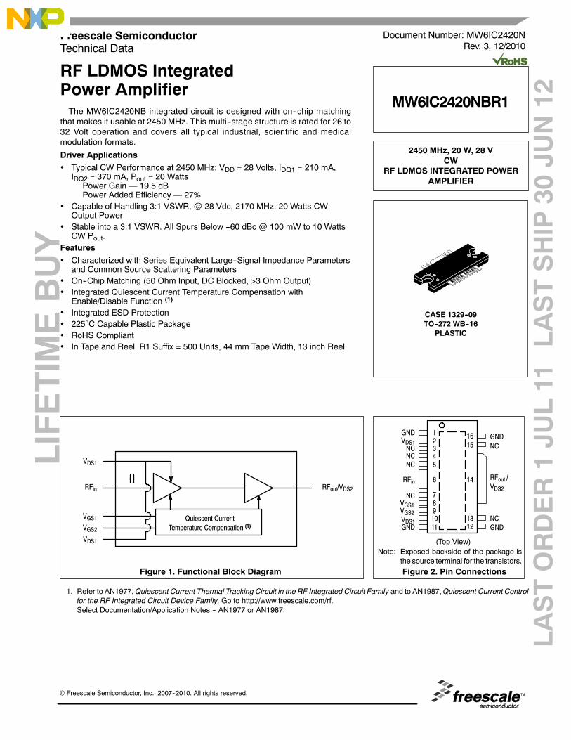
RF LDMOS IntegratedPower AmplifierThe MW6IC2420NB integrated circuit is designed with on--chip matching
that makes it usable at 2450 MHz. This multi--stage structure is rated for 26 to32 Volt operation and covers all typical industrial, scientific and medicalmodulation formats.
Driver Applications• Typical CW Performance at 2450 MHz: VDD = 28 Volts, IDQ1 = 210 mA,
IDQ2 = 370 mA, Pout = 20 WattsPower Gain — 19.5 dBPower Added Efficiency — 27%
• Capable of Handling 3:1 VSWR, @ 28 Vdc, 2170 MHz, 20 Watts CWOutput Power
• Stable into a 3:1 VSWR. All Spurs Below --60 dBc @ 100 mW to 10 WattsCW Pout.
Features• Characterized with Series Equivalent Large--Signal Impedance Parameters
and Common Source Scattering Parameters• On--Chip Matching (50 Ohm Input, DC Blocked, >3 Ohm Output)• Integrated Quiescent Current Temperature Compensation with
Enable/Disable Function (1)
• Integrated ESD Protection• 225°C Capable Plastic Package• RoHS Compliant• In Tape and Reel. R1 Suffix = 500 Units, 44 mm Tape Width, 13 inch Reel
Figure 1. Functional Block Diagram Figure 2. Pin Connections
(Top View)
GND
NC
RFin
VGS1
GND
RFout /VDS2
GND
12345
6
78
1615
14
1312
VGS2 910
GND 11Quiescent Current
Temperature Compensation (1)
VDS1
RFin
VGS1
RFout/VDS2
VGS2
VDS1NC
NC
NC
VDS1
NC
NC
VDS1
Note: Exposed backside of the package isthe source terminal for the transistors.
1. Refer to AN1977,Quiescent Current Thermal Tracking Circuit in the RF Integrated Circuit Family and to AN1987,Quiescent Current Controlfor the RF Integrated Circuit Device Family. Go to http://www.freescale.com/rf.Select Documentation/Application Notes -- AN1977 or AN1987.
LIFETIMEBUY
LASTORDER1JU
L11
LASTSHIP
30JU
N12
Document Number: MW6IC2420NRev. 3, 12/2010
Freescale SemiconductorTechnical Data
2450 MHz, 20 W, 28 VCW
RF LDMOS INTEGRATED POWERAMPLIFIER
MW6IC2420NBR1
CASE 1329--09TO--272 WB--16
PLASTIC
© Freescale Semiconductor, Inc., 2007--2010. All rights reserved.
2RF Device Data
Freescale Semiconductor
MW6IC2420NBR1
Table 1. Maximum Ratings
Rating Symbol Value Unit
Drain--Source Voltage VDSS --0.5, +68 Vdc
Gate--Source Voltage VGS --0.5, +6 Vdc
Storage Temperature Range Tstg --65 to +150 °C
Case Operating Temperature TC 150 °C
Operating Junction Temperature (1,2) TJ 225 °C
Input Power Pin 23 dBm
Table 2. Thermal Characteristics
Characteristic Symbol Value (2,3) Unit
Thermal Resistance, Junction to Case
W--CDMA Application Stage 1, 28 Vdc, IDQ = 210 mA(Pout = 4.5 W Avg.) Stage 2, 28 Vdc, IDQ = 370 mA
RθJC
1.81
°C/W
Table 3. ESD Protection Characteristics
Test Methodology Class
Human Body Model (per JESD22--A114) 1A (Minimum)
Machine Model (per EIA/JESD22--A115) A (Minimum)
Charge Device Model (per JESD22--C101) III (Minimum)
Table 4. Moisture Sensitivity Level
Test Methodology Rating Package PeakTemperature
Unit
Per JESD 22--A113, IPC/JEDEC J--STD--020 3 260 °C
Table 5. Electrical Characteristics (TA = 25°C unless otherwise noted)
Characteristic Symbol Min Typ Max Unit
Functional Tests (In Freescale Wideband 2110--2170 MHz Test Fixture, 50 ohm system) VDD = 28 Vdc, IDQ1 = 210 mA, IDQ2 = 370 mA,Pout = 4.5 W Avg., f1 = 2157.5 MHz, f2 = 2167.5 MHz, 2--Carrier W--CDMA, 3.84 MHz Channel Bandwidth Carriers. ACPR measured in3.84 MHz Channel Bandwidth @ ±5 MHz Offset. IM3 measured in 3.84 MHz Channel Bandwidth @ ±10 MHz Offset. Input SignalPAR = 8.5 dB @ 0.01% Probability on CCDF.
Power Gain Gps 25.5 28 30 dB
Power Added Efficiency PAE 13.7 15 — %
Intermodulation Distortion IM3 — --43 --40 dBc
Adjacent Channel Power Ratio ACPR — --46 --43 dBc
Input Return Loss IRL — --15 --10 dB
1. Continuous use at maximum temperature will affect MTTF.2. MTTF calculator available at http://www.freescale.com/rf. Select Software & Tools/Development Tools/Calculators to access
MTTF calculators by product.3. Refer to AN1955, Thermal Measurement Methodology of RF Power Amplifiers. Go to http://www.freescale.com/rf.
Select Documentation/Application Notes -- AN1955.(continued)
LIFETIMEBUY
LASTORDER1JU
L11
LASTSHIP
30JU
N12
MW6IC2420NBR1
3RF Device DataFreescale Semiconductor
Table 5. Electrical Characteristics (TA = 25°C unless otherwise noted) (continued)
Characteristic Symbol Min Typ Max Unit
Typical Performances (In Freescale Test Fixture, 50 ohm system) VDD = 28 Vdc, IDQ1 = 210 mA, IDQ2 = 370 mA, 2110--2170 MHz
Video Bandwidth @ 20 W PEP Pout where IM3 = --30 dBc(Tone Spacing from 100 kHz to VBW)∆IMD3 = IMD3 @ VBW frequency -- IMD3 @ 100 kHz <1 dBc (bothsidebands)
VBW— 30 —
MHz
Quiescent Current Accuracy over Temperaturewith 18 kΩ Gate Feed Resistors (--10 to 85°C) (1)
∆IQT — ±5 — %
Gain Flatness in 30 MHz Bandwidth @ Pout = 1 W CW GF — 0.2 — dB
Average Deviation from Linear Phase in 30 MHz Bandwidth@ Pout = 1 W CW
Φ — 2 — °
Average Group Delay @ Pout = 1 W CW Including Output Matching Delay — 2.8 — ns
Part--to--Part Insertion Phase Variation @ Pout = 1 W CW,Six Sigma Window
∆Φ — 18 — °
Table 6. Electrical Characteristics (TA = 25°C unless otherwise noted)
Characteristic Symbol Min Typ Max Unit
Typical Performances (In Freescale Test Fixture, 50 ohm system) VDD = 28 Vdc, IDQ1 = 110 mA, IDQ2 = 370 mA, 2110--2170 MHz
Saturated Pulsed Output Power(8 μsec(on), 1 msec(off))
Psat — 60 — W
1. Refer toAN1977,QuiescentCurrent Thermal TrackingCircuit in theRF IntegratedCircuit Family and toAN1987,QuiescentCurrentControlfor the RF Integrated Circuit Device Family. Go to http://www.freescale.com/rf.Select Documentation/Application Notes -- AN1977 or AN1987.
LIFETIMEBUY
LASTORDER1JU
L11
LASTSHIP
30JU
N12
4RF Device Data
Freescale Semiconductor
MW6IC2420NBR1
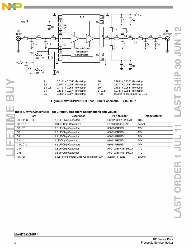
Figure 3. MW6IC2420NBR1 Test Circuit Schematic — 2450 MHz
Z6 0.189″ x 0.237″ MicrostripZ7 0.127″ x 0.054″ MicrostripZ9 0.182″ x 0.054″ MicrostripZ10, Z11 1.073″ x 0.054″ MicrostripPCB Taconic RF35, 0.020″, εr = 3.5
Z1 0.510″ x 0.054″ MicrostripZ2 0.300″ x 0.054″ MicrostripZ3, Z8 0.410″ x 0.054″ MicrostripZ4 0.138″ x 0.237″ MicrostripZ5 0.086″ x 0.237″ Microstrip
R1
Z2
RFINPUT
VGS1
Z4 Z5
RFOUTPUT
C8
VDS21
2
3
4
5
6
7
8
14
13
1211
10
9
15
16
NC
NC
NC
NC
NC
DUT
Z3
C1
VDS1
Z10
Quiescent CurrentTemperatureCompensation
Z1
Z11
Z6 Z7 Z8
C4 C12
C7C14 C15
C13
C5
R2
C3
VGS
VGS2 NC
NC
C2 C11
Z9
C10C9
C6
Table 7. MW6IC2420NBR1 Test Circuit Component Designations and ValuesPart Description Part Number Manufacturer
C1, C2, C3, C4 2.2 μF Chip Capacitors C32225X5R1H225MT TDK
C5, C13 100 nF Chip Capacitors C1206C104K1KAC Kemet
C6, C7 0.5 pF Chip Capacitors 08051J0R5BS AVX
C8 6.8 pF Chip Capacitor 08051J6R8BS AVX
C9 2.2 pF Chip Capacitor 08051J2R2BS AVX
C10 1 pF Chip Capacitor 08051J1R0BS AVX
C11, C12 5.6 pF Chip Capacitors 08051J5R6BS AVX
C14 0.3 pF Chip Capacitor ATC100B0R3BT500XT ATC
C15 0.5 pF Chip Capacitor ATC100B0R5BT500XT ATC
R1, R2 5 kΩ Potentiometer CMS Cermet Multi--turn 3224W--1--502E BournsLIFETIMEBUY
LASTORDER1JU
L11
LASTSHIP
30JU
N12
MW6IC2420NBR1
5RF Device DataFreescale Semiconductor
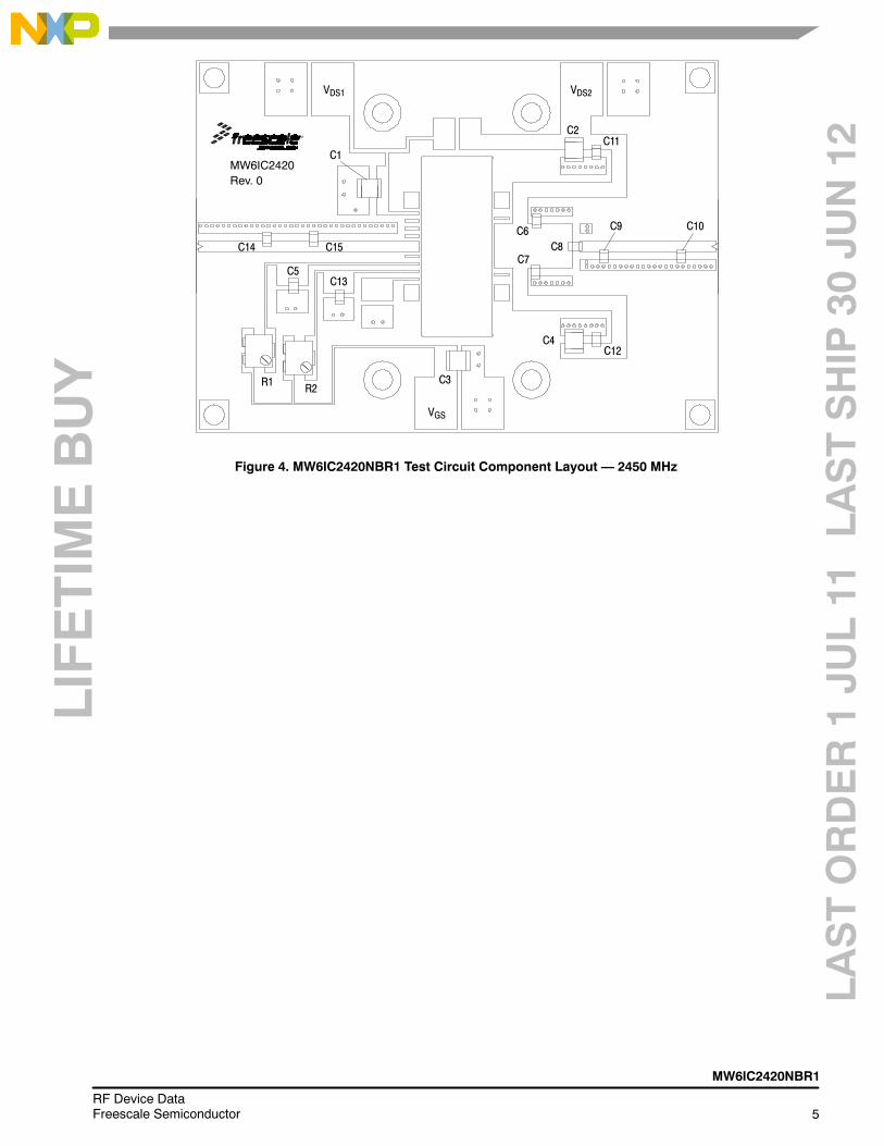
Figure 4. MW6IC2420NBR1 Test Circuit Component Layout — 2450 MHz
C1MW6IC2420
VDS1
Rev. 0
VDS2
VGS
C14 C15
C5C13
R1 R2C3
C4C12
C10C9
C7
C6C8
C2C11
LIFETIMEBUY
LASTORDER1JU
L11
LASTSHIP
30JU
N12
6RF Device Data
Freescale Semiconductor
MW6IC2420NBR1
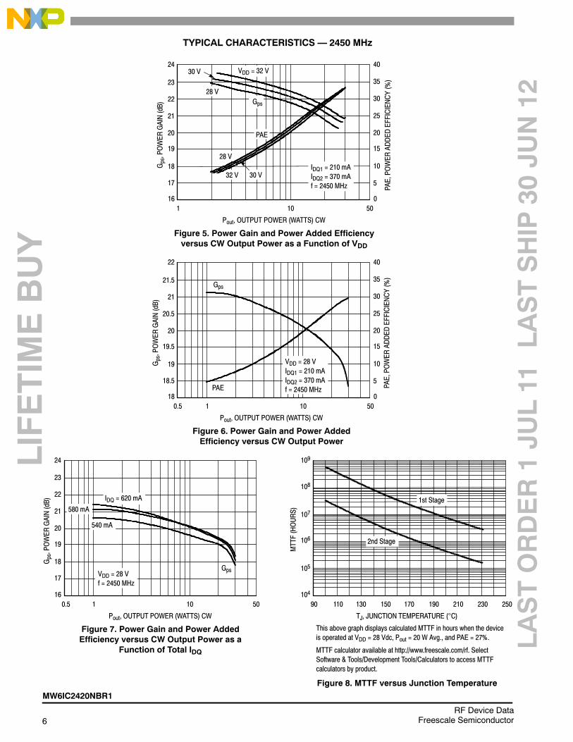
TYPICAL CHARACTERISTICS — 2450 MHz
Gps,POWER
GAIN(dB)
10
40
Gps
Pout, OUTPUT POWER (WATTS) CW
Figure 5. Power Gain and Power Added Efficiencyversus CW Output Power as a Function of VDD
IDQ1 = 210 mAIDQ2 = 370 mAf = 2450 MHz
10
30
20
10
16
24
23
21
19
PAE,POWER
ADDED
EFFICIENCY(%)
PAE
32 V 30 V
22
20
18
17
35
25
15
5
VDD = 32 V
28 V
30 V
28 V
50
Gps,POWER
GAIN(dB)
10
40
Gps
Pout, OUTPUT POWER (WATTS) CW
Figure 6. Power Gain and Power AddedEfficiency versus CW Output Power
10
30
20
10
18
22
21.5
20.5
19.5
PAE,POWER
ADDED
EFFICIENCY(%)
21
20
19
18.5
35
25
15
5
0.5 50
PAE
VDD = 28 VIDQ1 = 210 mAIDQ2 = 370 mAf = 2450 MHz
Gps,POWER
GAIN(dB)
0.5
Gps
Pout, OUTPUT POWER (WATTS) CW
Figure 7. Power Gain and Power AddedEfficiency versus CW Output Power as a
Function of Total IDQ
VDD = 28 Vf = 2450 MHz
16
24
23
21
19
22
20
18
17
IDQ = 620 mA
580 mA
1 10 50
540 mA
250
109
90
TJ, JUNCTION TEMPERATURE (°C)
Figure 8. MTTF versus Junction Temperature
This above graph displays calculated MTTF in hours when the deviceis operated at VDD = 28 Vdc, Pout = 20 W Avg., and PAE = 27%.
MTTF calculator available at http://www.freescale.com/rf. SelectSoftware & Tools/Development Tools/Calculators to access MTTFcalculators by product.
108
107
104
110 130 150 170 190
MTTF(HOURS)
210 230
2nd Stage
1st Stage
106
105
LIFETIMEBUY
LASTORDER1JU
L11
LASTSHIP
30JU
N12
MW6IC2420NBR1
7RF Device DataFreescale Semiconductor
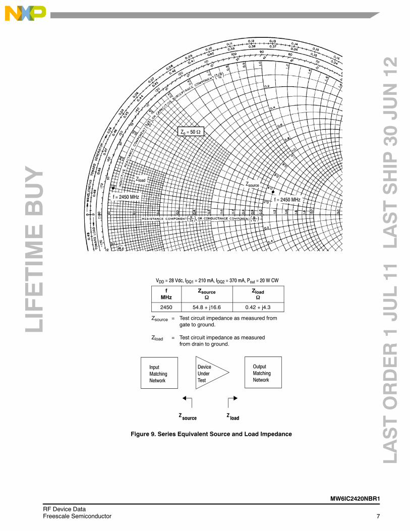
Zo = 50Ω
ZloadZsource
f = 2450 MHzf = 2450 MHz
VDD = 28 Vdc, IDQ1 = 210 mA, IDQ2 = 370 mA, Pout = 20 W CW
fMHz
ZsourceΩ
ZloadΩ
2450 54.8 + j16.6 0.42 + j4.3
Zsource = Test circuit impedance as measured fromgate to ground.
Zload = Test circuit impedance as measuredfrom drain to ground.
Zsource Z load
InputMatchingNetwork
DeviceUnderTest
OutputMatchingNetwork
Figure 9. Series Equivalent Source and Load Impedance
LIFETIMEBUY
LASTORDER1JU
L11
LASTSHIP
30JU
N12
8RF Device Data
Freescale Semiconductor
MW6IC2420NBR1
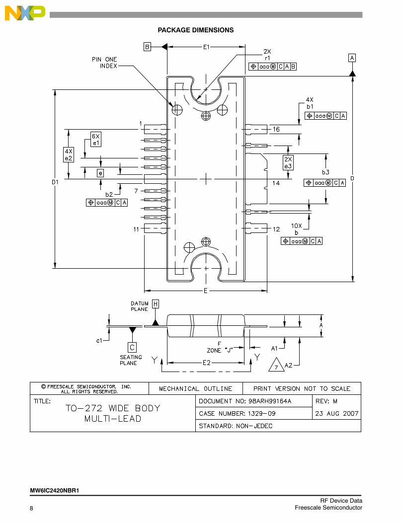
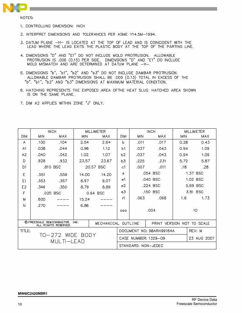
PACKAGE DIMENSIONS
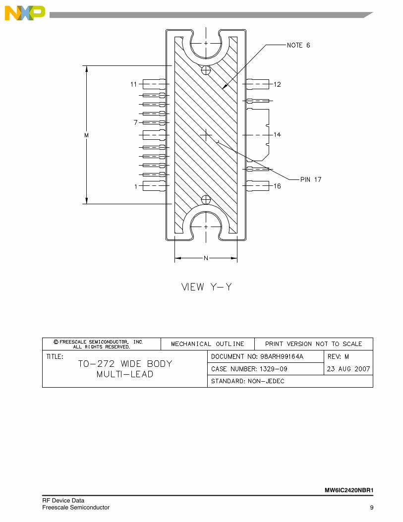
MW6IC2420NBR1
9RF Device DataFreescale Semiconductor
10RF Device Data
Freescale Semiconductor
MW6IC2420NBR1
MW6IC2420NBR1
11RF Device DataFreescale Semiconductor
PRODUCT DOCUMENTATION
Refer to the following documents to aid your design process.
Application Notes• AN1907: Solder Reflow Attach Method for High Power RF Devices in Plastic Packages
• AN1955: Thermal Measurement Methodology of RF Power Amplifiers
• AN1977: Quiescent Current Thermal Tracking Circuit in the RF Integrated Circuit Family
• AN1987: Quiescent Current Control for the RF Integrated Circuit Device Family
• AN3263: Bolt Down Mounting Method for High Power RF Transistors and RFICs in Over--Molded Plastic Packages
Engineering Bulletins• EB212: Using Data Sheet Impedances for RF LDMOS Devices
REVISION HISTORY
The following table summarizes revisions to this document.
Revision Date Description
0 Mar. 2007 • Initial Release of Data Sheet
1 Apr. 2008 • Changed 220°C to 225°C in Capable Plastic Package bullet, p. 1
• Added Footnote 1 to Quiescent Current Temperature bullet under Features section and to callout in Fig. 1,Functional Block Diagram, p. 1
• Added Case Operating Temperature limit to the Maximum Ratings table and set limit to 150°C, p. 2
• Operating Junction Temperature increased from 200°C to 225°C in Maximum Ratings table and related“Continuous use at maximum temperature will affect MTTF” footnote added, p. 2
• Replaced Case Outline 1329--09, Issue L, with 1329--09, Issue M, p. 8--10. Added pin numbers 1 through17.
2 Feb. 2009 • Changed Storage Temperature Range in Max Ratings table from --65 to +200 to --65 to +150 forstandardization across products, p. 2
• Modified data sheet to reflect RF Test Reduction described in Product and Process Change Notificationnumber, PCN13232, p. 2
3 Dec. 2010 • Corrected data sheet to reflect RF Test Reduction described in Product and Process Change Notificationnumber, PCN13232, and Product Discontinuance Notification number, PCN14260, adding applicableoverlay, p. 1, 2
LIFETIMEBUY
LASTORDER1JU
L11
LASTSHIP
30JU
N12
12RF Device Data
Freescale Semiconductor
MW6IC2420NBR1
Information in this document is provided solely to enable system and softwareimplementers to use Freescale Semiconductor products. There are no express orimplied copyright licenses granted hereunder to design or fabricate any integratedcircuits or integrated circuits based on the information in this document.
Freescale Semiconductor reserves the right to make changes without further notice toany products herein. Freescale Semiconductor makes no warranty, representation orguarantee regarding the suitability of its products for any particular purpose, nor doesFreescale Semiconductor assume any liability arising out of the application or use ofany product or circuit, and specifically disclaims any and all liability, including withoutlimitation consequential or incidental damages. “Typical” parameters that may beprovided in Freescale Semiconductor data sheets and/or specifications can and dovary in different applications and actual performance may vary over time. All operatingparameters, including “Typicals”, must be validated for each customer application bycustomer’s technical experts. Freescale Semiconductor does not convey any licenseunder its patent rights nor the rights of others. Freescale Semiconductor products arenot designed, intended, or authorized for use as components in systems intended forsurgical implant into the body, or other applications intended to support or sustain life,or for any other application in which the failure of the Freescale Semiconductor productcould create a situation where personal injury or death may occur. Should Buyerpurchase or use Freescale Semiconductor products for any such unintended orunauthorized application, Buyer shall indemnify and hold Freescale Semiconductorand its officers, employees, subsidiaries, affiliates, and distributors harmless against allclaims, costs, damages, and expenses, and reasonable attorney fees arising out of,directly or indirectly, any claim of personal injury or death associated with suchunintended or unauthorized use, even if such claim alleges that FreescaleSemiconductor was negligent regarding the design or manufacture of the part.
Freescalet and the Freescale logo are trademarks of Freescale Semiconductor, Inc.All other product or service names are the property of their respective owners.© Freescale Semiconductor, Inc. 2007--2010. All rights reserved.
How to Reach Us:
Home Page:www.freescale.com
Web Support:http://www.freescale.com/support
USA/Europe or Locations Not Listed:Freescale Semiconductor, Inc.Technical Information Center, EL5162100 East Elliot RoadTempe, Arizona 852841--800--521--6274 or +1--480--768--2130www.freescale.com/support
Europe, Middle East, and Africa:Freescale Halbleiter Deutschland GmbHTechnical Information CenterSchatzbogen 781829 Muenchen, Germany+44 1296 380 456 (English)+46 8 52200080 (English)+49 89 92103 559 (German)+33 1 69 35 48 48 (French)www.freescale.com/support
Japan:Freescale Semiconductor Japan Ltd.HeadquartersARCO Tower 15F1--8--1, Shimo--Meguro, Meguro--ku,Tokyo 153--0064Japan0120 191014 or +81 3 5437 [email protected]
Asia/Pacific:Freescale Semiconductor China Ltd.Exchange Building 23FNo. 118 Jianguo RoadChaoyang DistrictBeijing 100022China+86 10 5879 [email protected]
For Literature Requests Only:Freescale Semiconductor Literature Distribution Center1--800--441--2447 or +1--303--675--2140Fax: [email protected]
Document Number: MW6IC2420NRev. 3, 12/2010