Embed Size (px)
Citation preview
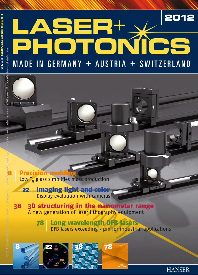
78 Long wavelength DFB lasersDFB lasers exceeding 3 µm for industrial applications
22 Imaging light and colorDisplay evaluation with cameras
8 Precision molding Low Tg glass simplifies mass production
8 22 38 78
M A D E I N G E R M A N Y + A U S T R I A + S W I T Z E R L A N D
38 3D structuring in the nanometer rangeA new generation of laser lithography equipment
LA
SER
+PH
OTO
NIC
S 2
012
2012
01_LPX_Titel_Owis_2012 15.12.2011 15:59 Uhr Seite 1
© 2
012
Car
l Han
ser V
erla
g, M
unic
h, G
erm
any
w
ww
.lase
r-ph
oton
ics.
eu
Not
for u
se in
inte
rnet
or i
ntra
net s
ites.
Not
for e
lect
roni
c di
strib
utio
n.

High-speed video analysis for motorsport 3D evaluation of high-speed videos is well known,
for example, in safety analysis and from motion
analysis in sports. But high-speed recordings can
also provide valuable information in motorsport,
particularly motorcycle racing.
48
2 l LASER+PHOTONICS 2 0 12 lCONTENT
MICRO-OPTICS
04 Ingeneric Microlens arrays as key elements for efficient colli-mation and homogenization.
06 Schott - Advanced Optics Low Tg glasses for use in precision molding.
TEST & MEASUREMENT
22 Instrument Systems Light and color measurement through imaging.
26 zygoLOT Scanning Fizeau interferometry for the deterministicsurface correction of precision aspheres.
POSITIONING
36 Owis New flip mirror holders for beam redirection, evenupside down.
38 Physik Instrumente / nanoscribe 3D structuring in the nanometer range demandshigh precision positioning.
IMAGE PROCESSING
48 PCO
SCENE
52 Jenoptik
56 Laser Zentrum Hannover 25 years after it opened, LZH looks towards futureresearch in energy, mobility and life sciences.
60 SPECTARIS Optical technologies made in Germany.
MATERIALS PROCESSING
66 Raylase
70 Rofin-Lasag Efficient and reproducible laser welding of copper.
LASER TECHNOLOGY
76 Innolight Compact sub-ns laser sources with simple designand huge potential.
78 nanoplus DFB lasers exceeding 3 µm for industrial applications.
84 EdgeWave Ultrafast Innoslab lasers with 400 W power.
86 Optotune Reducing laser speckle with new actuator technology.
89 TRADE DIRECTORY
90 IMPRINT
90 INDEX
Product Marketplace on pages: 16, 34, 46, 64, 69, 82, 88
Jenoptik turns 20 A broad-ranging
interview with the
Heads of the Jenop-
tik divisions ›Lasers
& Material Process-
ing‹ and ›Optical
Systems‹ on the
20th anniversary of
the Group.
52
66
More precisebeam deflection
High brightness
lasers and increas-
ing complexity of
production
processes mean
that scanning sys-
tems for materials
processing have to
up their game.
02-03_Inhalt_Edi_LPex2012 NEU 16.12.2011 14:08 Uhr Seite 2
© 2
012
Car
l Han
ser V
erla
g, M
unic
h, G
erm
any
w
ww
.lase
r-ph
oton
ics.
eu
Not
for u
se in
inte
rnet
or i
ntra
net s
ites.
Not
for e
lect
roni
c di
strib
utio
n.
MICRO-EPSILON94496 Ortenburg / GermanyTel. +49 85 42/[email protected]
CONFOCAL HIGH-ENDCONTROLLER
www.micro-epsilon.com
Latest high-end controller for displacement and thickness measurement Fast measurement on changing surfaces
For high precision measurements
World’s fastest controller (70kHz xenon / 10kHz LED)
Ethercat, Ethernet, RS422 and analogue
Standard sensors ø 21mm, can also be applied for single-sided thickness measurement
World‘s smallest miniature sensors (ø 4mm) with axial or radial beam path are ideal for themeasurement of bore holes and depressions
NEW
l3EDITORIAL
As usual, in this issue of Laser+Photonics: Made in Germany,Austria & Switzerland you will find a selection of the best
Laser+Photonik articles published in 2011 – but in English. Some of
these articles are freely available in the archive in our new web portal
(www.laser-photonik.de) where we also feature industry highlights
and products (largely) from the European region. Supplementary to
these previous articles you will find some brand new contributions.
All of the articles originate from companies and institutions based
within the German-speaking regions of Europe – Germany, Austria
and Switzerland. The raison d’être of the magazine is, in fact, to
provide those outside of these regions with a glimpse of the industry
within.
Laser+Photonik celebrated its 10th anniversary in 2011, and a num-
ber of (other) heavy weights of the photonics scene had something to
celebrate too: Jenoptik observed its 20th anniversary, the Laser
Zentrum Hannover looked back on 25 years of industrial R&D (p. 56)
and Newport’s Spectra Physics celebrated 50 years since its
founding. Incidentally, this edition features a genuinely interesting
interview with the Heads of the two Jenoptik divisions Lasers &
Material Processing and Optical Systems, the joint activities of these
divisiond forming the central core of Jenoptik’s commitment to the
photonics industry. You can read about Jenoptik’s strategy and the
Heads’ obervations on the market starting on p. 52.
But 2011 has been an interesting year for many other reasons too.
Company reports for turnover and profit have returned to levels that
would almost suggest that the recent financial crisis had never
occurred. Confidence in the market returned with avengence in 2011,
as indicated, for example, by Carl Zeiss achieving over 4 billion Euros
turnover for the very first time. Which is just as well, as the next
economic situation for Europe may be lurking just around the corner.
Confidencereturns
Dr. Gregory Flinn, [email protected]
02-03_Inhalt_Edi_LPex2012 NEU 16.12.2011 14:08 Uhr Seite 3
© 2
012
Car
l Han
ser V
erla
g, M
unic
h, G
erm
any
w
ww
.lase
r-ph
oton
ics.
eu
Not
for u
se in
inte
rnet
or i
ntra
net s
ites.
Not
for e
lect
roni
c di
strib
utio
n.

VOLKER S INHOFF
STEFAN HAMBÜCKER
OLAF RÜBENACH
CHRIST IAN WESSL ING
For a long time, microoptics have been an indispensi-
ble component of the system design for shaping the
beam of high power semiconductor lasers – whether
in the form of fast and slow axis optics for collimation or
symmetrization of the laser beam, or in the form of beam
transformation optics for efficient fiber coupling. For many
innovative applications – from display production in electri-
cal engineering, to the interaction of laser radiation with the
skin in medical technology, through to the use of special
beam profiles in sensor and measurement technology – a
significant improvement in the homo-
geneity of the laser beam is a critical
requirement when using semicon-
ductor lasers. Likewise, for the next
generation of laser diode types, ap-
propriate collimation optics need to be
developed and be manufacturable on
a large scale.
Microcylinder lens arrays
There are several different methods for the homogenization of
laser radiation. For example, homogenization of a specified
beam profile, for example a Gaussian beam, can be achieved
using specially shaped aspheres. The disadvantage of this
solution is the high sensitivity of the homogenization result in
terms of fluctuations in the initial beam profile and the assem-
bly accuracy. Another method for homogenization of laser
radiation is the use of waveguides or optical fibers. However,
this method requires a sophisticated assembly process and
sufficient installation space.
Homogenization using microcylinder lens arrays is a consider-
ably more elegant and compact solution. In this case, the inci-
dent laser beam is separated into partial beams by one or more
microlens arrays. These partial beams are then overlaid in the
homogenization plane by the downstream
optics. Depending on the arrangement and
geometry of the microlenses, this enables
homogeneous illuminated lines, rectangles or
squares to be generated. The major advantage
of this solution lies in the huge scope for ad-
justment to account for the initial beam pro-
file, as well as the extremely compact design.
4 l LASER+PHOTONICS 2 0 12 lOPTICS
INGENERIC GmbH 52068 Aachen, Germany
Tel. +49 (0)241 963-1340
www.ingeneric.com
CONTACT
Microlens arrays ALTHOUGH MICROOPTICS can now be found in many applications,
microlens arrays made of highly refractive optical glass occupy a rather
special position. Because of their technical properties, they are important for
a variety of new high power laser applications.
04-07_LPX110101_ingeneric_LPex2012 ax 15.12.2011 16:08 Uhr Seite 4
© 2
012
Car
l Han
ser V
erla
g, M
unic
h, G
erm
any
w
ww
.lase
r-ph
oton
ics.
eu
Not
for u
se in
inte
rnet
or i
ntra
net s
ites.
Not
for e
lect
roni
c di
strib
utio
n.

Only the highest quality
The crucial requirements for the fault-
free performance of the microcylinder
lens array are sufficient high damage
threshold, high contour accuracy, and
the minimum possible dead zone
between the lens segments.
The damage threshold is determined
by the glass itself and the surface coat-
ing. Typical limit values for the optical
intensity are around 150 kW/cm2,
which is met by both quartz glass and
highly refractive optical glass. In terms
of contour accuracy, it is not just the
shape of the individual lens segments
that is crucial, but particularly the re-
peat accuracy and the pitch accuracy
(the spacing and positioning of the lens
segments relative to one another). To
guarantee fault-free imaging, the re-
quired accuracies fall into the sub-micrometer range. The dead
zone describes the area immediately between the lens
segments and, because of technical production limitations, can-
not typically be described deterministically. The larger the dead
zone, the higher the radiation losses and so too the variations
from the desired homogeneity. The exact manufacturing
method has a crucial influence on the size of the dead zone,
although modern techniques can achieve values as low as
around ±40 to 50 µm.
The latest generation of XP microcylinder lens arrays from
Ingeneric is tailor-made for the tasks outlined above. The
›Xtreme Precision‹ arrays provide fault-free imaging and opti-
mum light output. This is guaranteed by the extremely high
component quality and minimization of the dead zones between
the lens elements (in this case less than 20 µm). Following
optical analysis of the microcylinder lens array using a stereo
microscope and plane parallel plate, this property is recognizable
through the extremely thin line width (Figure 1, right). Because
OPTICS l LASER+PHOTONICS 20 12 l5
pco.edge – the first camera systemwith the revolutionary sCMOS image sensor
Bringing to light! The new camera system pco.edge represents a perfectcombination of high resolution, extremely low read out noise, and superior dynamic – at low light, for excellent image quality even at high frame rates. Discover the new possibilities in the range of high performance applications. More information on www.pco.de/scmos-cameras/pcoedge/
high resolution
5.5 megapixel
readout noise
< 1.1med electrons
dynamic range
> 27000 : 1
maximum frame rate
100 frames / s
in America: www.cookecorp.com
1 Analysis of array quality using a stereo microscope and plane-parallel plate
© LASER+PHOTONICS
04-07_LPX110101_ingeneric_LPex2012 ax 15.12.2011 16:08 Uhr Seite 5
© 2
012
Car
l Han
ser V
erla
g, M
unic
h, G
erm
any
w
ww
.lase
r-ph
oton
ics.
eu
Not
for u
se in
inte
rnet
or i
ntra
net s
ites.
Not
for e
lect
roni
c di
strib
utio
n.
of the excellent contour accuracy, the arrays also have an
extremely constant focal position. To illustrate the quality dif-
ference, Figure 1 compares an optimum cylinder lens array and
an array with deficiencies in terms of the focal position.
All arrays are produced from highly refractive and highly trans-
parent optical glass to ensure reliable operation with high laser
powers. Focal lengths of 2.2 to 7.3 mm and pitch sizes of 0.2
to 1.0 mm are available as standard. In addition, customer-spe-
cific designs can be produced, as well as lens arrays exhibiting
a large height profile relative to the spacing of the lens segments.
Arrays with rotationally
symmetrical aperture
While crossed cylinder lens arrays generate a rectangular flat
top profile, the output beam profile when using arrays with
a rotationally symmetrical aperture is circular. The general
conditions with regard to the design and production require-
ments for the arrays are comparable with those for a cylindrical
structure.
However, as well as being able to homogenize laser beams,
this array structure is of particular interest for beam shaping of
VCSELs and LEDs. Arranging VCSELs in a row enables optical
powers ranging from several 100 W and up into the kilowatt
range to be achieved. The advantage over edge emitting diodes
is the cost effectiveness of VCSELs, as they can be complete-
ly processed at wafer level all the way along the production
chain and are very durable in use.
The design freedom of the VCSEL arrays therefore results in
tough requirements for the lens arrays, which are used for
collimation of the laser light. As well as varying the distance
between the VCSELs, the shape of the emitting region can
also vary from circular. In terms of the appropriate optics, there
may thus be a future demand for micro-freeform optics
arranged as high performance arrays.
When it comes to the design, the advantage of Ingeneric ar-
rays (Figure 2) lies in the use of highly refractive optical glass.
For example, complex designs with tough demands on the
apertures can be translated into structures suitable for manu-
facture. Typical apertures for manufactured lens arrays range
from 0.5 to 3.0 mm, while focal lengths scale from 0.7 mm for
extremely short focal length requirements on up to 25.0 mm.
The standard pitch is between 0.2 and 3.0 mm. To ensure a
high fill ratio for hexagonal arrangements, the selected pitch
between the lenses can be smaller than the aperture, in which
case the lenses literally overlap.
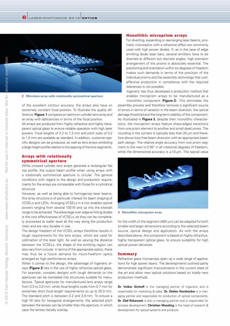
Monolithic microprism arrays
For diverting, expanding or rearranging laser beams, pris-
matic microoptics with a refractive effect are commonly
used with high power diodes. If, as in the case of edge
emitting diode laser bars, several emitters have to be
diverted at different but discrete angles, high precision
arrangement of the prisms is absolutely essential. The
positioning and orientation within six degrees of freedom
makes such demands in terms of the precision of the
individual prisms and the assembly technology that cost-
effective production in compliance with the required
tolerances is not possible.
Ingeneric has thus developed a production method that
enables microprism arrays to be manufactured as a
monolithic component (Figure 3). This eliminates the
assembly process and therefore removes a significant source
of errors in terms of variation in the beam diversion, the optical
damage threshold and the long-term stability of the component.
As illustrated in Figure 3, despite their monolithic character-
istics, the microprism arrays feature sharp-edged transitions
from one prism element to another and small dead zones. The
rounding in the corners is typically less than 20 µm and there-
fore allows loss-free beam diversion with an appropriate beam
path design. The relative angle accuracy from one prism seg-
ment to the next is 0.05° in all rotational degrees of freedom,
while the dimensional accuracy is ±10 µm. The typical value
for the width of the segment (400 µm) can be adapted for both
smaller and larger dimensions according to the selected beam
source, optical design and application. As with the arrays
described above, this component is based on highly refractive,
highly transparent optical glass, to ensure suitability for high
optical power densities.
Summary
Refractive glass microarrays open up a wide range of applica-
tions for high power lasers. The developments outlined partly
demonstrate significant improvements in the current state of
the art and allow new optical solutions based on totally new
production methods.
Dr. Volker Sinhoff is the managing partner of Ingeneric and is
responsible for marketing & sales. Dr. Stefan Hambücker is a man-
aging partner and responsible for production of optical components.
Dr. Olaf Rübenach is also a managing partner and is responsible for
process development. Christian Wessling is the head of research &
development for optical systems and products.
6 l LASER+PHOTONICS 2 0 12 lOPTICS
2 Microlens array with rotationally symmetrical aperture
3 Monolithic microprism array
04-07_LPX110101_ingeneric_LPex2012 ax 15.12.2011 16:08 Uhr Seite 6
© 2
012
Car
l Han
ser V
erla
g, M
unic
h, G
erm
any
w
ww
.lase
r-ph
oton
ics.
eu
Not
for u
se in
inte
rnet
or i
ntra
net s
ites.
Not
for e
lect
roni
c di
strib
utio
n.
www.scanlab.de
NEW: intellicube® 14
Wondering how to create a high-end laser processing system despite intense cost pressure?Use SCANLAB’s intellicube® – the smallest smart scan head with high-performance dynamics.
The intellicube® combines the advantages of SCANLAB’s successful SCANcube® and intelliSCAN® scan head platforms:
Want to know if intellicube® is the right scan system for your application? Contact us at [email protected].
More information at:
04-07_LPX110101_ingeneric_LPex2012 ax 15.12.2011 16:08 Uhr Seite 7
© 2
012
Car
l Han
ser V
erla
g, M
unic
h, G
erm
any
w
ww
.lase
r-ph
oton
ics.
eu
Not
for u
se in
inte
rnet
or i
ntra
net s
ites.
Not
for e
lect
roni
c di
strib
utio
n.
RALF JEDAMZIK
RALF B IERTÜMPFEL
Precision molding is the most modern method for mass
production of complex lens shapes. In fact, it even
enables high surface quality directly following the hot
forming process. Nevertheless, the unique properties of the
glass materials used in this field also need to be taken into
account, and Schott has therefore developed special glass
types that best meet the manufacturing requirements. In
addition, the company is constantly expanding its product
range in this area.
Classic grinding and polishing
Traditional manufacturing consists of a multi-stage process in
which a raw glass block is formed into a lens blank using cutting
and grinding processes. These lens blanks are then polished
(depending on the requirements) using either a typical CNC-
controlled polishing method or a modern magnetorheological
finishing for aspherical surfaces.
Using hot pressed lens blanks is one way to simplify mass
production. During the hot pressing process, blocks of the
initial glass with a predefined volume are
pressed into a so-called preform. The
preform corresponds to the desired final
outline to within a few millimeters, and the
desired final shape and quality is achieved
using traditional processes.
Using the pressing process saves CNC
processing time, and thus makes lens
manufacturing more economical, although the ideal solution
would be for the glass to be brought into its final shape direct-
ly using a hot forming process. In any case, the optical surface
still needs to meet the requirements for shape, roughness and
maximum number of allowed defects to the highest extent
possible, and precision blank pressing is indeed able to meet
these requirements.
Precision molding of complex geometries
Precision molding is now the method of choice when it comes
to cost-effective mass production of optical components with
complex geometries. Typical applications include aspherical
lenses for cell phones, projectors and compact cameras (Fig-ure 1), lens arrays for LED lighting (Figure 2), but also micro-
optical components such as diffractive optical elements and
nanostructures. These all require a preform with high surface
quality.
Appropriate preforms include spherical lenses, polished rods,
polished disks or precision gobs created directly from the glass
melt. One thing that all preforms have in common is that they
can be manufactured very cost-effectively and are made of a
special glass well suited for the precision molding process. They
can be used to manufacture aspherical
lenses of variable sizes and geometries
(Figure 3), for instance.
Manufacturing of optical components with
a diameter of less than 40 mm has now
proven to be most economical. Typical
surface radii for aspherical geometries are
then between 0.8 and 250 mm. Maximum
8 l LASER+PHOTONICS 2 0 12 lOPTICS
SCHOTT AG, Advanced Optics55122 Mainz, Germany
Tel. +49 (0)6131 66-1812
Fax +49 (0)3641 288-9054
www.schott.com/advanced_optics
CONTACT
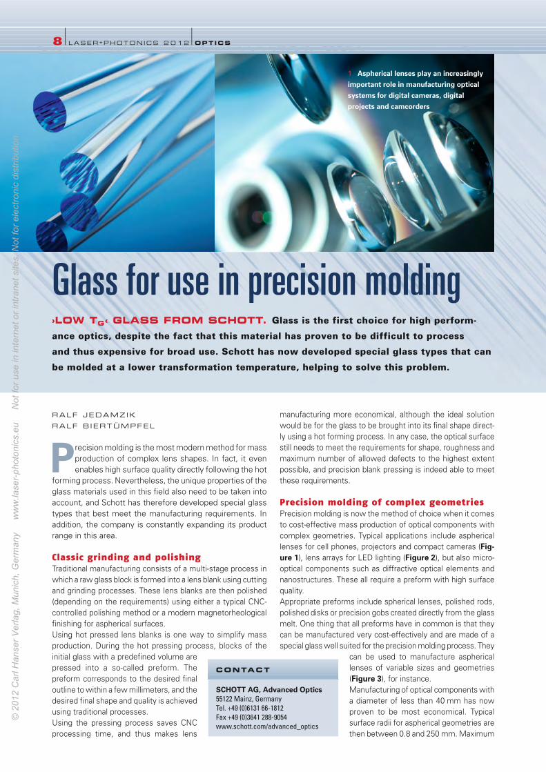
1 Aspherical lenses play an increasinglyimportant role in manufacturing opticalsystems for digital cameras, digitalprojects and camcorders
Glass for use in precision molding›LOW TG‹ GLASS FROM SCHOTT. Glass is the first choice for high perform-
ance optics, despite the fact that this material has proven to be difficult to process
and thus expensive for broad use. Schott has now developed special glass types that can
be molded at a lower transformation temperature, helping to solve this problem.
08-11_LPX110108_schott_LPex2012 ax 15.12.2011 16:11 Uhr Seite 8
© 2
012
Car
l Han
ser V
erla
g, M
unic
h, G
erm
any
w
ww
.lase
r-ph
oton
ics.
eu
Not
for u
se in
inte
rnet
or i
ntra
net s
ites.
Not
for e
lect
roni
c di
strib
utio
n.
precision can be achieved if extreme aspect ratios between the
thickness of the edge and center are avoided. On plane surface
sections, small deviations can either be tolerated or polished
out later. Surfaces with a slight radius are more stable and can
therefore be molded more precisely.
Molding without sticking
Precision molding applies principles from the manufacture of
polymer optics to that of glass, although this isn’t actually a
simple task because, unlike polymers, glass is an inorganic
material with strong atomic bonds. This means that high tem-
peratures are often necessary for molding. In addition, each
glass has its own characteristic viscosity depending on the
temperature.
During traditional hot pressing, glass is pressed in a low vis-
cosity range at high temperatures of between 750 and 1500°C.
To prevent the glass from adhering to the mold, separating
agents or steep temperature gradients must be used between
the glass and the mold. This alters the surface texture and the
shape of the pressed optic, however, therefore reworking is
necessary in order to achieve high accuracy.
By contrast, precision molding is performed at lower tempera-
tures of between 500 and 900°C with significantly higher
viscosities. In order to reproduce the desired shape accurately
and achieve high surface quality, the pressing mold itself must
be optically polished. It is nearly always impossible to use a
separator in such cases because this would have a negative
effect on the molding results. The high glass viscosity prevents
the optic from adhering to the mold anyway.
Giving glass its shape
The accuracy of the mold determines the precision of the
pressed optic. When creating the mold, the designer must also
take proper account of the thermal properties of the glass, such
as the shrinkage of the optic after the hot molding process. Be-
cause the mold design is a significant cost factor in the blank
pressing process, it is important to make sure the mold can be
used for as long as possible.
The molds are usually produced from tungsten carbide or sili-
con carbide. These can contain a binder such as cobalt in the
structure, although these chemical elements could diffuse into
the glass and lead to discoloration on the surface. For this rea-
son, the molds are given different coatings normally based on
precious metals (Pt, Au, Ir, Rh) or carbon. These prevent the
glass from reacting with or adhering to the mold material.
The cleaning processes used with glass preforms must be
strictly controlled so that they do not result in soluble compo-
nents of the glass structure being drawn out of the surface, as
this could adversely influence the surface quality that can be
achieved after pressing. It is also important to avoid potential
vaporization processes of substances from the glass surface at
the high temperatures used during pressing, as these can con-
densate on the surface of the mold and shorten its service life.
Controlling quality
The design of an optical system defines the requirements for
the material, shape and surface quality of its components. With
precision molding, the accuracy of the pressed optic is deter-
mined by the quality of the mold and by monitoring the tem-
perature closely over time. The number of macroscopic defects
on the surface and their roughness depend on how much time
the pressing process consumed and how much pressure was
applied, but also on the initial
surface quality of both the
mold and the preform.
The quality of the optical glass
used is also critical, which
means that the initial material
should be free from bubbles
and inclusions and should have
a reproducibly high homo-
geneity. On the other hand,
both the molds and the mold-
ing machine would have to
meet high demands with re-
spect to their temperature
stability if glass types with a
high transformation tempera-
ture (high Tg) were to be used
in precision molding. For this
reason, Schott has developed
a range of special glass types
OPTICS l LASER+PHOTONICS 2012 l9
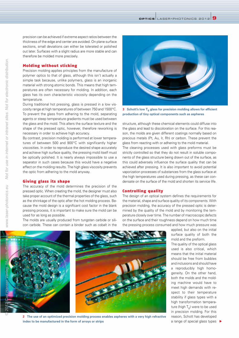
2 The use of an optimized precision molding process enables aspheres with a very high refractiveindex to be manufactured in the form of arrays or strips
3 Schott’s low Tg glass for precision molding allows for efficientproduction of tiny optical components such as aspheres
08-11_LPX110108_schott_LPex2012 ax 15.12.2011 16:11 Uhr Seite 9
© 2
012
Car
l Han
ser V
erla
g, M
unic
h, G
erm
any
w
ww
.lase
r-ph
oton
ics.
eu
Not
for u
se in
inte
rnet
or i
ntra
net s
ites.
Not
for e
lect
roni
c di
strib
utio
n.
that can be processed at much lower temperatures (under
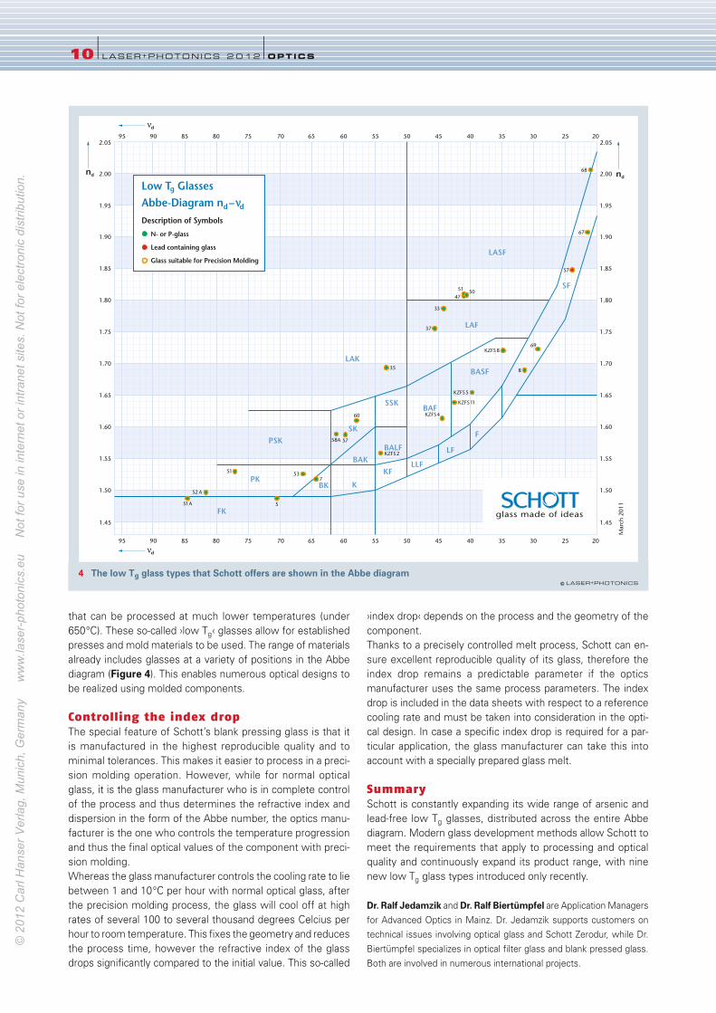
650°C). These so-called ›low Tg‹ glasses allow for established
presses and mold materials to be used. The range of materials
already includes glasses at a variety of positions in the Abbe
diagram (Figure 4). This enables numerous optical designs to
be realized using molded components.
Controlling the index drop
The special feature of Schott’s blank pressing glass is that it
is manufactured in the highest reproducible quality and to
minimal tolerances. This makes it easier to process in a preci-
sion molding operation. However, while for normal optical
glass, it is the glass manufacturer who is in complete control
of the process and thus determines the refractive index and
dispersion in the form of the Abbe number, the optics manu-
facturer is the one who controls the temperature progression
and thus the final optical values of the component with preci-
sion molding.
Whereas the glass manufacturer controls the cooling rate to lie
between 1 and 10°C per hour with normal optical glass, after
the precision molding process, the glass will cool off at high
rates of several 100 to several thousand degrees Celcius per
hour to room temperature. This fixes the geometry and reduces
the process time, however the refractive index of the glass
drops significantly compared to the initial value. This so-called
›index drop‹ depends on the process and the geometry of the
component.
Thanks to a precisely controlled melt process, Schott can en-
sure excellent reproducible quality of its glass, therefore the
index drop remains a predictable parameter if the optics
manufacturer uses the same process parameters. The index
drop is included in the data sheets with respect to a reference
cooling rate and must be taken into consideration in the opti-
cal design. In case a specific index drop is required for a par-
ticular application, the glass manufacturer can take this into
account with a specially prepared glass melt.
Summary
Schott is constantly expanding its wide range of arsenic and
lead-free low Tg glasses, distributed across the entire Abbe
diagram. Modern glass development methods allow Schott to
meet the requirements that apply to processing and optical
quality and continuously expand its product range, with nine
new low Tg glass types introduced only recently.
Dr. Ralf Jedamzik and Dr. Ralf Biertümpfel are Application Managers
for Advanced Optics in Mainz. Dr. Jedamzik supports customers on
technical issues involving optical glass and Schott Zerodur, while Dr.
Biertümpfel specializes in optical filter glass and blank pressed glass.
Both are involved in numerous international projects.
10 l LASER+PHOTONICS 2 0 12 lOPTICS
Low Tg GlassesAbbe-Diagram nd –ννd
Description of Symbols
N- or P-glass
Lead containing glass
Glass suitable for Precision Molding
PSK
FK
PK
LAK
BK K
SK
LLF
BALF
BAFSSK
BASF
F
SF
LASF
LF
LAF
KF
BAK
KZFS4
57
KZFS2
5
51
51A
52 A
KZFS8
KZFS5
KZFS11
33
67
57
8
47
51 50
58A
60
35
68
69
37
νd
νd
1.45
1.50
1.55
1.60
1.65
1.70
1.75
1.80
1.85
1.90
1.95
2.00
2.05
1.45
1.50
1.55
1.60
1.65
1.70
1.75
1.80
1.85
1.90
1.95
2.00
2.05
nd
85 80 75 70 65 60 55 50 45 40 35 30 25 209095
85 80 75 70 65 60 55 50 45 40 35 30 25 209095
nd
Mar
ch 2
011
753
4 The low Tg glass types that Schott offers are shown in the Abbe diagram © LASER+PHOTONICS
08-11_LPX110108_schott_LPex2012 ax 15.12.2011 16:11 Uhr Seite 10
© 2
012
Car
l Han
ser V
erla
g, M
unic
h, G
erm
any
w
ww
.lase
r-ph
oton
ics.
eu
Not
for u
se in
inte
rnet
or i
ntra
net s
ites.
Not
for e
lect
roni
c di
strib
utio
n.
08-11_LPX110108_schott_LPex2012 ax 15.12.2011 16:11 Uhr Seite 11
© 2
012
Car
l Han
ser V
erla
g, M
unic
h, G
erm
any
w
ww
.lase
r-ph
oton
ics.
eu
Not
for u
se in
inte
rnet
or i
ntra
net s
ites.
Not
for e
lect
roni
c di
strib
utio
n.
12 lCOMPANY PROF ILE
COMPANY PROF ILE
Fresnel Optics GmbH – Our expertise foryour success
Fresnel Optics GmbH, part of Reflexite Energy
Solutions, is a market leader in the design and
fabrication of plastic micro- and nanostructured
optical components for the lighting, solar pow-
er, instrumentation and display industries. Prod-
ucts include optics and lenses that enhance ar-
chitectural lighting, solar concentrator lenses
and lens arrays, optical light enhancing films
and a variety of components that improve the
performance and efficiency of your optical
system. We offer standard products and cus-
tom fabrication as well as sample and series
production. For quality assurance we work
according to DIN ISO 9001:2008.
Our Capabilities– Experience in optical and mechanical design
– Precision mastering (diamond turning, flycut-
ting, linear ruling, laser writing)
– State-of-the-art tool replication (electroform-
ing and plating)
– Precision polymer replication (compression
and injection molding, polymer-on-glass
processing)
– Custom finishing (trimming, printing)
– Product enhancement processes (AR-struc-
tures / coatings, aluminum and hard coat-
ing)
– Subassembly processes
Our Products– Fresnel lenses
– Fresnel cylinder lenses
– Fresnel prisms and beam splitters
– Micro-lens arrays
– Hybrid optics such as Silicone-on-Glass
(SOG) lens parquets for CPV applications
Fresnel Optics GmbHFlurstedter Marktweg 13
99510 Apolda, Germany
Phone +49 (0)3644 5011-0
Fax +49 (0)3644 5011-50
www.fresnel-optics.de
LAYERTEC, established in 1990 as a spin off
from the Friedrich-Schiller-Universität Jena,
produces high quality optical components for
laser applications in the wavelength range from
the VUV (157nm) to the NIR (~4µm).
The company combines a precision optics
facility and a variety of coating techniques
(magnetron sputtering, thermal and e-beam
evaporation).
The precision optics facility of LAYERTEC
produces plane and spherically curved mirror
substrates, lenses and prisms of fused silica,
optical glasses like BK7 and some crystalline
materials, e. g. calcium fluoride. Fused silica
and calcium fluoride can be offered with rms-
roughnesses as low as 0.15nm.
Components for the UV are coated by evapo-
ration techniques. Coatings for the VIS and NIR
are mostly produced by magnetron sputtering.
This special coating process yields amorphous
layers with a very high packing density result-
ing in lowest straylight losses and a high ther-
mal and climatical stability of the optical param-
eters. Furthermore, the coatings are optimized
for high laser damage thresholds. LAYERTEC
has developed magnetron sputtering for opti-
cal coatings from a laboratory technique to a
very efficient industrial process.
The main products of LAYERTEC are· High – power - coatings for the NIR (e.g. for
Nd:YAG-, Ho:YAG- and Er:YAG-lasers)
· Femtosecond laser mirrors with exactly
determined phase properties (low GDD or
negative GDD and R>99.9%)
· Steep edge filters, e.g. HR 1030nm >99.9%
+ R(980nm)<1% with high laser damage
thresholds
· Low loss laser mirrors (R>99.99 in the VIS
and NIR)
· Coatings on laser- and nonlinear optical crys-
tals
· Metallic mirrors and coatings (Au, Ag, Al, Cr)
· Coatings for all excimer laser wavelengths
including 157nm
Besides the development of efficient coating
plants LAYERTEC has preserved its capabili-
ties for flexible production and the develop-
ment of prototypes and OEM components.
LAYERTEC – optische Beschichtungen GmbH
Ernst-Abbe-Weg 1
99441 Mellingen
Germany
Phone +49 (0)36453 744-0
Fax +49 (0)36453 744-40
www.layertec.de
_FP_LPex2012 14.12.2011 15:31 Uhr Seite 12
© 2
012
Car
l Han
ser V
erla
g, M
unic
h, G
erm
any
w
ww
.lase
r-ph
oton
ics.
eu
Not
for u
se in
inte
rnet
or i
ntra
net s
ites.
Not
for e
lect
roni
c di
strib
utio
n.
COMPANY PROF ILE l13
FISBA OPTIK AGOptical Solutions
Rorschacherstrasse 268
9016 St. Gallen, Switzerland
Phone: 0041 (0)71 282 31 31
Fax: 0041 (0)71 282 31 30
www.fisba.com
FISBA OPTIK AGFISBA OPTIK is a world leader in optical sys-
tems, instruments and components. At FISBA
we develop and produce high-grade solutions
in the field of micro- and macro-optics. From
simple lenses to complex optical components
and systems, the optical solutions created by
FISBA are perfectly tailored to the specific cus-
tomer needs.
All aspects of optical expertise underone roof
FISBA unites all required disciplines and expert
knowledge under one roof. Lens designers and
engineers, backed by specialists in physics and
coating technology, develop, analyze and opti-
mize optical systems and components for the
entire spec¬tral range from UV to NIR — inte-
grated and sustainable.
New technologies for affordableglass optics
FISBA employs and develops leading technolo-
gies to provide outstanding results for every
production stage, from prototypes tocomplex
optics in large-scale production. Uncompromis-
ing quality control vouches for flawless prod-
ucts that render incoming goods inspection su-
perfluous, saving valuable time and in¬creas-
ing process stability.
Newest technologies are implemented not on-
ly to offer customers the best optic solutions
for their application but at a reasonable price
as well. FISBA employs precision glass mold-
ing for the production of glass optics with ar-
bitrary forms in larger lots at a fair price, open-
ing up totally new possibilities in the cus-
tomer’s system development and assembly
optimization.
Product Portfolio
Advanced Optical Components
• Precision molded lenses
• Fast axis collimation lenses (FACs)
• FISBA Beam Twister™
• Aspheres
Optical Systems
• Lens systems
• Objectives
• Laser Modules
• Laser Optics
• Collimators
• Illumination
Optical Microsystems
Application Fields
• Biophotonics
• Bildverarbeitung und Sensorik
• Industrielle Fertigung
• Sicherheit und Verteidigung
• Weltraum und Astonomie
_FP_LPex2012 14.12.2011 15:31 Uhr Seite 13
© 2
012
Car
l Han
ser V
erla
g, M
unic
h, G
erm
any
w
ww
.lase
r-ph
oton
ics.
eu
Not
for u
se in
inte
rnet
or i
ntra
net s
ites.
Not
for e
lect
roni
c di
strib
utio
n.
MÖLLER-WEDEL OPTICAL GmbHRosengarten 10
22880 Wedel
Germany
Phone +49 (0)4103 93776-10
FAX +49 (0)4103 93776-60
www.moeller-wedel-optical.com
MOELLER-WEDEL OPTICAL GmbH, a sub-
sidiary of MÖLLER-WEDEL GmbH, concen-
trates on high-precision optical test equipment
for industry and science.
ProductsThe different lines of electronic autocollima-tors ELCOMAT cover the most common
measurement tasks in industry and science:
ELCOMAT HR for ultra precision measure-
ment and calibration tasks with an accuracy up
to 0.01 arcsec, ELCOMAT 3000 for extremely
precise alignment and angular measurements
with an accuracy up to 0.1 arcsec and a meas-
urement range of 2000 arcsec, ELCOMAT vario
product line as well as of ELCOMAT direct
product line for precise angular measurement
and adjustment with an accuracy between
3 arcsec and 0.3 arcsec. Moreover, ELCOMAT
direct series enables the user to evaluate mul-
tiple autocollimation images and thus to meas-
ure wedges, prism angles etc. directly.
The measuring combination for lenses andoptical systems MELOS 530 provides fast and
reliable measurement of most relevant optical
parameter, i.e. focal lengths, back focal
lengths, radii of curvature.
The low cost VI-vario interferometer line can
be used to measure plane and spherical optics
such as mirrors, prisms, cubes or lenses.
The Goniometer II allows the accurate meas-
urement of prism angles with an accuracy of
0.6 arcsec, the GONIOMETER-SPECTROME-
TER VIS enables the measurement of refrac-
tive index in the visual range with an accuracy
of 10–5.
The new GONIOMAT M is a unique user-friend-
ly semiautomatic portable goniometer that
is able to measure angles of prisms, polygons
and wedges with an accuracy of up to 1.5 arc-
sec.
Well known visual collimators, autocollima-tors, testing telescopes, diopter telescopesand alignment systems complete the exten-
sive range of products.
BERLINER GLAS GROUP - High technologysolutions in OEM opticsThe BERLINER GLAS GROUP has extensive
OEM expertise in a wide varity of application
areas including.
· Space based optical systems
· Lasers and laser based systems
· Medical and life science
· Geosystems
· Metrology
· Defense
· Semiconductor
With approximately 1.000 employes, BERLIN-
ER GLAS GROUP provides tailor-made, mar-
ket-driven OEM solutions of the highest quali-
ty. From design to production we are your OEM
partner.
Engineering
System engineering · Optical and mechanical
design · Coating design · Customer-specific
metrology
Key-Components
Spherical lenses · Aspherical lenses · Cylindri-
cal lenses · Plano optics · Prism systems · Mi-
crostructuring · Coating: coating design, spec-
tral range: VUV, DUV, UV, VIS, NIR, IR · Anti-
reflex coatings · Filter · Mirror · Beam splitter/
combiner · Holographic gratings · ITO coating
Assemblies Systems
Optical assemblies and systems (cemented
beam splitter, prism systems, doublets,
triplets, step-system) · Optomechanical as-
semblies and systems · Electro-optical sys-
tems · Lens systems · Objectives, zoom sys-
tems · Measuring systems · Cameras · Laser
systems · Light sources · Lighting systems
14 lCOMPANY PROF ILE
COMPANY PROF ILE
Berliner Glas KGaAHerbert Kubatz GmbH & Co.Waldkraiburger Str. 5
12347 Berlin, Germany
Phone +49 (0)30 60905-0
SwissOptic AGHeinrich-Wild-Strasse
9435 Heerbrugg, Switzerland
Phone: +41 (0)71 727-3074
www.berlinerglasgroup.com
_FP_LPex2012 14.12.2011 15:31 Uhr Seite 14
© 2
012
Car
l Han
ser V
erla
g, M
unic
h, G
erm
any
w
ww
.lase
r-ph
oton
ics.
eu
Not
for u
se in
inte
rnet
or i
ntra
net s
ites.
Not
for e
lect
roni
c di
strib
utio
n.
COMPANY PROF ILE l15
Docter Optics GmbHMittelweg 29
07806 Neustadt an der Orla
Germany
Phone +49 36481 27-0
Fax +49 36481 27-270
www.docteroptics.com
Establishments:Docter OpticsExpress Glass ServicesDocter Optics GmbH
Str. der Deutschen Einheit 6
07819 Triptis, Germany
Phone +49(0)36481 27-350
Fax +49(0)36481 27-369
Docter OpticsNorth AmericaDocter Optics, Inc.
1425 West Elliot Road, Suite A-105
Gilbert, AZ 85233, USA
Phone +1 480 844-7585
Fax +1 480 844-7826
Docter OpticsJapanGeneral Bldg., 2F
No. 25-20,
Sakashita 1-Chome
Itabashi-ku, Tokyo 174-0043, Japan
Phone +81(0)3 3969 3731
Fax +81(0)3 3969 3732
Docter Optics ChinaGuangzhou Office
2911 Metro Plaza, No.183 Tianhe
North Road, 510620 Guangzhou
China
Phone +86 - 20 - 2222 1020
Fax +86 - 20 - 8755 1889
DOCTER OPTICS – Turning Ideas IntoComponents
Docter Optics has earned international re-
cognition as an OEM partner of the optical
technology sector and a leading supplier to
the automobile industry. Headquartered in
Germany’s “Optical Valley” with presences in
China, Japan and the USA, the company offers
customers services along the entire added-
value chain. The company’s list of first-class
references from the areas of automotive, illu-
mination optics, concentrating photovoltaics,
biometrics, security and medical applications
testify to a track record of exceptional cus-
tomer- and market-driven performance.
Quality plus Efficiency: Precision GlassComponents
The Precision Glass Components division pro-
duces optical components such as light pipes
(concentrators) for advanced Concentrated
Photovoltaics (CPV) systems in large runs
using a process that makes it possible to mold
the glass as soon as it leaves the furnace. The
Precision Fast-Molding process developed by
Docter Optics permits production of precision
glass components, e.g. free-form-lenses, lens-
arrays/integrator plates, prisms, light pipes and
mirrors for high-end medical and analytical
equipment or illumination/LED applications.
The Precision Glass Components-value chain
encompasses:
· Custom design
· Mass production
· Ready molding
· Design freedom
· Cost effective solutions
· Optical Glass Doctan SG 2
A Single-Source Supplier: Optical Systems
The bundled competencies of the four Docter
Optics business units represent unique syner-
gistic potential, which makes Docter Optics
an industry leader in the development and pro-
duction of custom-tailored optical, optome-
chanic and optoelectronic subassemblies:
· Initial Development Partner
· Optical and Optomechanical design
· Assembling, prototyping and series produc-
tion
· Development of customer-specific testing
methods, procurement and logistic models
Top-Tier Services: Express Glass Services
The Express Glass Services unit ships semi-
finished products of optical glass to customers
worldwide and manufactures prototypes, sam-
ples and one-of-a-kind parts and can deliver pre-
production and limited quantities with extreme-
ly short lead times. An extensive inventory of
special glass qualities allows Express Glass
Services to react to customer needs quickly
and efficiently.
State-of-the-Art: Automotive Solutions
Docter Optics is the market leader in the area
of projection lenses of optical glass for auto-
motive headlights. Automated production
processes and use of DOC3D® for double-
sided precision-molded pro-
jection lenses give Docter
Optics a competitive ad-
vantage that permits quick
reaction times and precise
compliance with customer
quality specifications. Cus-
tomers can avail themselves
of a complete array of serv-
ices:
· Aspheric lenses, free-form
shapes and lens arrays for
projection headlights
· Development, design and
prototyping of new lens
shapes
· Adjustment of photomet-
ric characteristics of lens-
es for different light
sources (Halogen, HID,
LED) and regional stan-
dards (ECE, SAE)
· Textures and coatings
_FP_LPex2012 14.12.2011 15:31 Uhr Seite 15
© 2
012
Car
l Han
ser V
erla
g, M
unic
h, G
erm
any
w
ww
.lase
r-ph
oton
ics.
eu
Not
for u
se in
inte
rnet
or i
ntra
net s
ites.
Not
for e
lect
roni
c di
strib
utio
n.
For sophisticatedimage processing Lenses for cameras with 1“ sensors.Qioptiq’s new series of ›MeVis-CF‹ lens-
es offers high imaging performance in a
compact, rugged housing. Building on
their MeVis-C lenses for C-mount cam-
eras with sensor sizes of up to 1", the
new series features time-tested optics,
promising high resolution over the entire
image circle, low distortion and good
color correction, as well as low bright-
ness drop in an even more compact and
rugged housing to meet the most strin-
gent requirements. The fixed aperture
also helps to save space while prevent-
ing operator error. These lenses are avail-
able in a number of variants with differ-
ent apertures, making it possible to offer
customer-specific versions with special
aperture shapes.
www.qioptiq.com
Designed for short pulsesFused silica lenes. Sill Optics offers a se-
ries of fused silica ƒ-Theta lenses
optimized for use with short pulse (SP)
and ultrashort pulse (USP) lasers. A quasi-
telecentric ƒ-Theta lens (›S4LFT3161/
292‹) with a focal length of 163 mm
enables the laser beam to realize an inci-
dent angle of less than 5° at the edge a
the 90 x 90 mm2 scan field. Optimized for
wavelengths ranging from 515 to 545 nm,
the minimum spot size in the scan field
is about 15 µm with a beam diameter of
10 mm. As to the ›S4LFT3162/328‹ for
the infrared range of 1030 to 1090 nm,
the spot size is about 20 µm for a beam
diameter of 15 mm. Designed to achieve
even smaller spots, the telecentric lens
S4LFT4010/292 has a focal length of
100 mm and realizes at a field size of 35
x 35 mm2 an incidence angle of 1.4° with
a beam diameter of 10 mm. This lens is
also optimized for a wavelength range of
515 to 545 nm and enables a spot size of
about 9 µm. The ›S4LFT4010/328‹ is
designed for the infrared range from 1030
to 1090 nm and has a spot size of about
18 µm.
www.silloptics.de
16 l LASER+PHOTONICS 2 0 12 lPRODUCT MARKETPLACE
Lenses with F-mount... for industrial applications. Carl zeiss presents new F-mount lenses ideal for use
with high-resolution image sensors and larger sensor formats in industry and research.
The new high speed
›Distagon T* 1.4 / 35‹
delivers crisp, sharp
images even at maxi-
mum aperture open-
ing, thanks to its large
focus ring and precise
wormgear. The lens’
optical construction
also guarantees a high
image quality across
the entire image
range. Another lens
suitable for industry
and research is the
new high speed ›Distagon T* 2/25‹, a moderate wide-angle lens. It shows its strengths
especially with fast-moving objects or in tough lighting situations, as is often the case
in the industrial sector. It also offers an excellent color correction.
www.zeiss.de
16-17_produkte_LPex2012_x 15.12.2011 16:13 Uhr Seite 16
© 2
012
Car
l Han
ser V
erla
g, M
unic
h, G
erm
any
w
ww
.lase
r-ph
oton
ics.
eu
Not
for u
se in
inte
rnet
or i
ntra
net s
ites.
Not
for e
lect
roni
c di
strib
utio
n.
PRODUCT MARKETPLACE l LASER+PHOTONICS 20 12 l17
Fiber optics updateProduct catalogue 2012. In their product
catalogue 2012 ›Fiber Optics – Light
switching, Light transportation, Light dis-
tribution‹ Leoni Fiber Optics presents the
first multimode splitters produced by
means of ion exchange in glass. In addi-
tion to the extensive update, the chapters
›Fiber optic cables‹, ›Optical components‹,
›POF/PCF‹, ›Laser probes (medical de-
vices)‹ include a wide range of new prod-
ucts as well as a short overview of fiber
optical assemblies for harsh environ-
ments, such as in industrial applications
and in the energy sector. New products in
the sections ›LargeCore‹, ›Singlemode‹,
›Fiber bundles‹, ›Tubes and loose tubes‹
and ›Accessories‹ are clearly laid out. The
catalogue is available for download in the
›service‹ area on the website as well as in
print upon request via contact form.
www.leoni-fiber-optics.com
Preconfigured and codedFDN glass fiber closures for FTTH sec-tor. With their FDN closure, Ficonet sys-
tems is launching an FRBU for up to 144
fibers with heat shrink splice protection,
and whose capacity doubles to 288 fibers
with crimp splice protection, a solution
widely used in Germany. For customer
projects, the closure can be adapted to
specific requirements and fiber capacities
(up to 576 fibers) on request. Up to 61
ports are available for cable feeds, of
which 52 are cable inlets for cables or in-
jectors up to 9.5 mm. These apertures
have different sizes, making them suitable
for a huge variety of cable diameters. Un-
cut multi-fiber loose tube cables can also
be inserted and embedded. ›Cablelok‹ fit-
tings are used to seal the cables – these
are rubber sleeves that are sealed by feed-
ing in the cable opposite the body of the
closure. This system has been tested up
to a water column depth of 8 m. The FDN
closure can be fitted with various splice
trays containing heat shrink or crimp splice
protection or fiber splitters. If required, the
closure can be supplied completely pre-
assembled to customer specifications.
When using injectors, this allows fibers
from the splice tray or from an external
location to be injected into the splice tray
at distances of several hundred meters.
www.ficonet-shop.de
Flattop for NUV,VIS and NIRAchromatic beam shaping optics. Adl-
Optica has optimized their achromatic
refractive field mapping beam shapers
πShaper 6_6_NUV, πShaper 6_6_VIS,
πShaper 6_6_NIR to operate, respective-
ly, in near-UV (335 to 560 nm), Visual (420
to 680 nm) and near-IR (1100 to 1700 nm)
spectral bands. The πShaper 6_6 converts,
with nearly 100 percent efficiency, a
Gaussian laser beam into a flattop beam
of low divergence while keeping a uniform
intensity profile over a large working dis-
tance. The achromatic design ensures that
the same beam quality is maintained at
any wavelength of the working spectral
band and allows using several lasers of dif-
ferent wavelengths simultaneously. The
flat output phase front, similar input and
output beam sizes, the lack of internal fo-
cus, a high destruction threshhold and the
compact size facilitate integration in sys-
tems for scientific as well as industrial ap-
plications such as confocal microscopy,
flow cytometry, various fluorescence tech-
niques, mass-spectrometry, holography,
and micromachining, among others.
www.piShaper. com
pickpro stay ahead.
Stay ahead, pick pro
A Passion for Precision.
pro series @ TOPTICA
www.toptica.com/pro
16-17_produkte_LPex2012_x 15.12.2011 16:14 Uhr Seite 17
© 2
012
Car
l Han
ser V
erla
g, M
unic
h, G
erm
any
w
ww
.lase
r-ph
oton
ics.
eu
Not
for u
se in
inte
rnet
or i
ntra
net s
ites.
Not
for e
lect
roni
c di
strib
utio
n.
MARKUS SCHNITZLE IN
Machine vision systems are in
higher demand than ever before.
By means of special cameras
and computers, industrial production sys-
tems are taught how to ›see‹, in other
words, to inspect and make decisions ac-
cordingly. As a result, production process-
es can be designed to be safer and more
efficient. The applications are numerous
and range from completeness monitoring,
to surface inspection, identification and
robot guidance, to classic measuring tech-
nology.
Machine vision systems have never really
been a true alternative and were in every
sense inferior to the human eye when it came
to accurate color assessment. Despite the
fact that visual perception plays a far greater role for people
than other modes of perception, correct color reproduction has
hitherto played a lesser role within the context of automated
quality control.
Color control in printing technology
To ensure print quality, today’s modern printing machines are
often already equipped with machine vision systems. These
can be used to ensure the complete automated imaging of all
print elements and avoid possible errors, such as streaking.
Thus, the use of inline inspection systems to capture the spec-
tral properties of inks, for example, opens up new opportuni-
ties for automated machine control and ensures the improved
reproduction of the required colors.
Color used to be checked manually after the test sheets were
printed out. Using separate color measuring equipment, the
operator compared the target values and actual values and made
any necessary recalibrations. This was a time-consuming
process, which typically required several iterations. It is also
worth bearing in mind that visual color assessment is strongly
dependent on lighting conditions and that the color perception
of the human observer is restricted to three sensors (red, green,
and blue). The risk of an erroneous color perception is extremely
great under these conditions.
18 l LASER+PHOTONICS 2 0 12 lTEST & MEASUREMENT
Extrasensory color recognition12-CHANNEL SPECTRAL CAMERA. Chromasens presents a spectral inline
color measuring system that uses twelve filters to allow the spectral reconstruction
of the ink spectrum with a precision far greater than that of the human eye. This opens
up entirely new applications for machine vision and quality control.
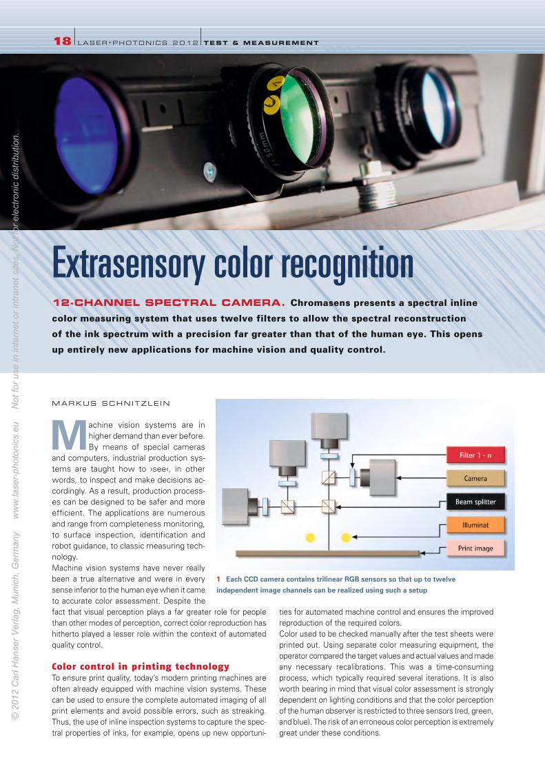
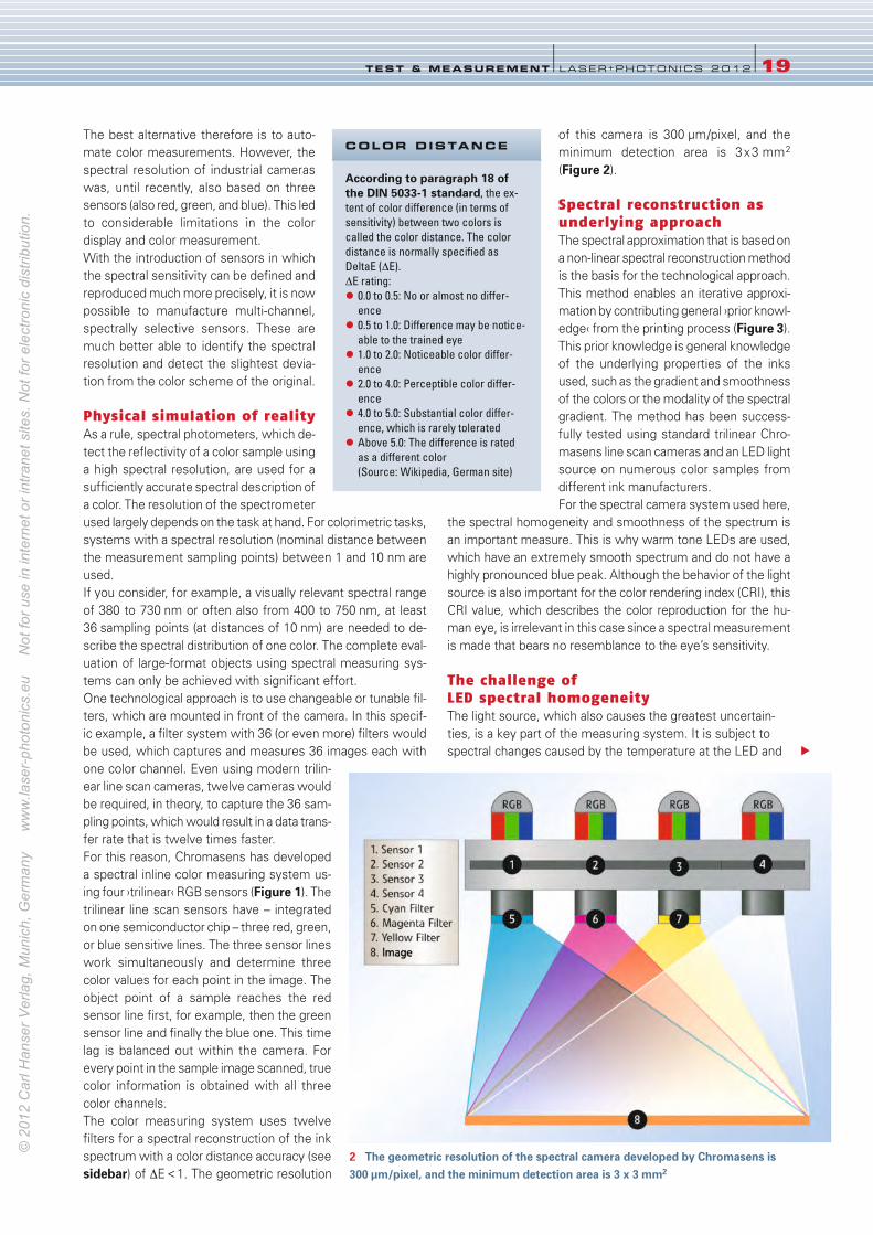
1 Each CCD camera contains trilinear RGB sensors so that up to twelve independent image channels can be realized using such a setup
18-20_LPX110092_chromasens_LPex2012_x 15.12.2011 16:17 Uhr Seite 18
© 2
012
Car
l Han
ser V
erla
g, M
unic
h, G
erm
any
w
ww
.lase
r-ph
oton
ics.
eu
Not
for u
se in
inte
rnet
or i
ntra
net s
ites.
Not
for e
lect
roni
c di
strib
utio
n.
The best alternative therefore is to auto-
mate color measurements. However, the
spectral resolution of industrial cameras
was, until recently, also based on three
sensors (also red, green, and blue). This led
to considerable limitations in the color
display and color measurement.
With the introduction of sensors in which
the spectral sensitivity can be defined and
reproduced much more precisely, it is now
possible to manufacture multi-channel,
spectrally selective sensors. These are
much better able to identify the spectral
resolution and detect the slightest devia-
tion from the color scheme of the original.
Physical simulation of reality
As a rule, spectral photometers, which de-
tect the reflectivity of a color sample using
a high spectral resolution, are used for a
sufficiently accurate spectral description of
a color. The resolution of the spectrometer
used largely depends on the task at hand. For colorimetric tasks,
systems with a spectral resolution (nominal distance between
the measurement sampling points) between 1 and 10 nm are
used.
If you consider, for example, a visually relevant spectral range
of 380 to 730 nm or often also from 400 to 750 nm, at least
36 sampling points (at distances of 10 nm) are needed to de-
scribe the spectral distribution of one color. The complete eval-
uation of large-format objects using spectral measuring sys-
tems can only be achieved with significant effort.
One technological approach is to use changeable or tunable fil-
ters, which are mounted in front of the camera. In this specif-
ic example, a filter system with 36 (or even more) filters would
be used, which captures and measures 36 images each with
one color channel. Even using modern trilin-
ear line scan cameras, twelve cameras would
be required, in theory, to capture the 36 sam-
pling points, which would result in a data trans-
fer rate that is twelve times faster.
For this reason, Chromasens has developed
a spectral inline color measuring system us-
ing four ›trilinear‹ RGB sensors (Figure 1). The
trilinear line scan sensors have – integrated
on one semiconductor chip – three red, green,
or blue sensitive lines. The three sensor lines
work simultaneously and determine three
color values for each point in the image. The
object point of a sample reaches the red
sensor line first, for example, then the green
sensor line and finally the blue one. This time
lag is balanced out within the camera. For
every point in the sample image scanned, true
color information is obtained with all three
color channels.
The color measuring system uses twelve
filters for a spectral reconstruction of the ink
spectrum with a color distance accuracy (see
sidebar) of ΔE <1. The geometric resolution
of this camera is 300 µm/pixel, and the
minimum detection area is 3x3 mm2
(Figure 2).
Spectral reconstruction as
underlying approach
The spectral approximation that is based on
a non-linear spectral reconstruction method
is the basis for the technological approach.
This method enables an iterative approxi-
mation by contributing general ›prior knowl-
edge‹ from the printing process (Figure 3).
This prior knowledge is general knowledge
of the underlying properties of the inks
used, such as the gradient and smoothness
of the colors or the modality of the spectral
gradient. The method has been success-
fully tested using standard trilinear Chro-
masens line scan cameras and an LED light
source on numerous color samples from
different ink manufacturers.
For the spectral camera system used here,
the spectral homogeneity and smoothness of the spectrum is
an important measure. This is why warm tone LEDs are used,
which have an extremely smooth spectrum and do not have a
highly pronounced blue peak. Although the behavior of the light
source is also important for the color rendering index (CRI), this
CRI value, which describes the color reproduction for the hu-
man eye, is irrelevant in this case since a spectral measurement
is made that bears no resemblance to the eye’s sensitivity.
The challenge of
LED spectral homogeneity
The light source, which also causes the greatest uncertain-
ties, is a key part of the measuring system. It is subject to
spectral changes caused by the temperature at the LED and
TEST & MEASUREMENT l LASER+PHOTONICS 2012 l19
According to paragraph 18 ofthe DIN 5033-1 standard, the ex-
tent of color difference (in terms of
sensitivity) between two colors is
called the color distance. The color
distance is normally specified as
DeltaE (ΔE).
ΔE rating:
� 0.0 to 0.5: No or almost no differ-
ence
� 0.5 to 1.0: Difference may be notice-
able to the trained eye
� 1.0 to 2.0: Noticeable color differ-
ence
� 2.0 to 4.0: Perceptible color differ-
ence
� 4.0 to 5.0: Substantial color differ-
ence, which is rarely tolerated
� Above 5.0: The difference is rated
as a different color
(Source: Wikipedia, German site)
COLOR DISTANCE
2 The geometric resolution of the spectral camera developed by Chromasens is300 µm/pixel, and the minimum detection area is 3 x 3 mm2
18-20_LPX110092_chromasens_LPex2012_x 15.12.2011 16:17 Uhr Seite 19
© 2
012
Car
l Han
ser V
erla
g, M
unic
h, G
erm
any
w
ww
.lase
r-ph
oton
ics.
eu
Not
for u
se in
inte
rnet
or i
ntra
net s
ites.
Not
for e
lect
roni
c di
strib
utio
n.

the impressed current. In addition, the light source ages and
thereby changes its emission spectrum. Chromasens has
taken the following counter measures:
� The current is kept constant – the LEDs therefore age at the
same rate.
� The LEDs are mounted on a cooling element to dissipate
the heat and homogenize heat distribution.
� The light emitted is bundled via a channel-shaped ellipsoid
mirror and thus focuses on one line. A large number of LEDs
in the LED line contribute to the intensity at one specific
location of the illuminated sample. As a result, the different
spectra of the LEDs are mixed thoroughly.
� A spectral measurement of the LED illumination is taken at
each location in the line before installation. This is the most
time-consuming part. Over the service life of the LED, the
spectrum is constantly measured at one specific location
and included in the spectral reconstruction.
It must be emphasized here that the system does not need to
be calibrated. The LED line can be replaced without recalibrat-
ing the camera. However, the module-specific spectral data of
the new LED line must be incorporated in the spectral recon-
struction.
The particular advantage of this approach is that the filters used
and their spectral characteristics can, to a large extent, be freely
selected. The functionality of the solution is not reduced to the
use of particularly narrow band filters. Thanks to the flexibility
of the reconstruction algorithms, this method can correct
differences in the spectral detection caused by the different
angles of incidence of the light on the sensor and the color fil-
ter. Thus, the accuracy of the spectral estimation is no longer
subject to any immediate dependency on the sampling location.
The ›truePIXA-6C‹ technology, developed by Chromasens to-
gether with the Constance University of Applied Sciences and
the Chemnitz University of Technology, is now ready for the
market and for use. It enables multi-channel image acquisition
within the RGB and infrared area (360 to 950 nm). The enhanced
versions ›truePIXA-9C‹ and ›truePIXA-12C‹ can be used for
measurement applications in the area of spectral reconstruc-
tions of the originals. Once calibrated in the factory, the spec-
tral properties of the camera system are extremely stable and
do not require any further readjustments. For implementation
on the customer side, only the spectral properties of the light
source used need to be captured. This
is usually done via a white balance
measurement.
Spectral camera opens up
new applications
While it may take some time for the
commercial use of spectral image
acquisition to become more wide-
spread, this method can be used any-
where today where camera systems
and measuring systems are needed for
high precision image acquisition and
color measurement.
A good example is print quality control,
where the use of inline inspection sys-
tems to capture the spectral properties
of inks unlocks new opportunities for
automated machine control. Other possible applications are to
be found in material sorting and classic production technology.
Besides these ›traditional‹ machine vision segments, the
targeted use of spectral cameras opens up a wide range of new
applications. In the field of safety engineering, for example,
official documents, such as passports, can be checked for
authenticity or products of unknown origin can be checked for
plagiarism. The product engineers also envisage many useful
applications in medical technology, such as in minimally inva-
sive surgery or remote diagnoses in the field of telemedicine.
In both these areas, images without chromatic aberrations –
for example, for assessing changes to the surface of the skin
– are jsut as important as optimizing the image contrast.
Summary
The spectral acquisition of objects
and the spectral reconstruction of
colors pave the way for new fields of
applications. Whereas the most pre-
cise spectral measurement of colors
and hence correct color reproduction
– within the context of automated
quality control – has hitherto played a lesser role, this will change
with the new technological approaches. Twelve-channel spec-
tral cameras are for the first time capable of detecting the most
minute color differences with a precision that is far beyond the
capability of the human eye. This opens up entirely new appli-
cations for machine vision.
Markus Schnitzlein is the Managing Director of Chromasens. Based
in Constance, Germany, the company develops and produces image
acquisition and image processing systems. The company’s expertise
includes both system and components development.
References1 Hardeberg, J.: ›Acquisition and Reproduction of Color Images‹, Up-
ublish.Com, 2001, www.dissertation.com/library/112135a.htm, IS-
BN 1-58112-135-0
2 Stark, H., Yang, Y.: ›Vector Space Projections‹, John Wiley & Sons,
1998, ISBN 0-471-24140-7
3 Hill, B.: ›(R)evolution of Color Imaging Systems‹, Proc. 1st European
Conference on Color in Graphics, Imaging and Vision (CGIV) 2002
20 l LASER+PHOTONICS 2 0 12 lTEST & MEASUREMENT
3 The method is based on an iterative approach and has the advantage that underlying properties of the object to be measured can be applied numerically within the iteration processes
© LASER+PHOTONICS
Chromasens GmbH
78467 Konstanz, Germany
Tel. +49 (0)7531 876-0
Fax +49 (0)7531 876-303
www.chromasens.com
CONTACT
18-20_LPX110092_chromasens_LPex2012_x 15.12.2011 16:17 Uhr Seite 20
© 2
012
Car
l Han
ser V
erla
g, M
unic
h, G
erm
any
w
ww
.lase
r-ph
oton
ics.
eu
Not
for u
se in
inte
rnet
or i
ntra
net s
ites.
Not
for e
lect
roni
c di
strib
utio
n.

COMPANY PROF ILE l21
TRIOPTICS GmbHHafenstr. 35–39
22880 Wedel
Germany
Phone +49 (0)4103 18006 0
Fax +49 (0)4103 18006 20
www.trioptics.com
TRIOPTICSThe Whole Spectrum ofOptical Metrology…Since 1992 TRIOPTICS GmbH has been a lead-
ing manufacturer of optical test equipment for
industrial and scientific use. The company has
focused on research and development of ac-
curate and automatic optical test and measure-
ment instruments.
Products
ImageMaster® is the most comprehensive
line of MTF-equipment for complete charac-
terization of lenses and optical systems.
The OptiCentric® family comprises tools for
the precise and fully automatic alignment, ce-
menting, bonding and assembly of lenses and
optical systems. It includes the measurement
of multi-lens objectives in mounted conditions,
air gap distance and lens center thickness as
well as the individual centering error of aspher-
ical lenses.
OptiSpheric® is the industry´s standard for
integrated optical testing. It provides fast and
reliable test results of almost all relevant optical
parameters, i.e. effective focal length (EFL), mod-
ulation transfer function (MTF), back focal length
(BFL), radius of curvature (ROC) and flange focal
length (FFL). Extension modules include multi
wavelength and intraocular lens (IOL) testing.
The WaveSensor® and WaveMaster® provide
wavefront analysis of lenses or optical sys-
tems. Both comprise a highly accurate Shack-
Hartmann Sensor. The reflex module enables
to measure the shape of optical surfaces.
TriAngle®, the electronic autocollimator series
from TRIOPTICS provides angle, wedge and
straightness measurements for precision align-
ment tasks with excellent accuracy and high
speed.
PrismMaster® is the most accurate automa-
tic goniometer featuring angle measurements
of prisms, polygons and other plano optics with
accuracies better than 0.2 arcsec.
The SpectroMaster® offers the highest ac-
curacy measurement of the refractive index of
optical glass in spectral ranges from UV, across
VIS to IR.
µPhase® Interferometer qualifies the quality
of spherical, aspherical and flat optics. It is com-
pact and modular and measures optics and sur-
faces with reflectivities from 0.3% to 100%.
OptiCentric® 3D• Combining the known centering measurement
technology integrated in OptiCentric® with theOptiSurf® low coherence interferometer formeasuring the air gaps between lens elementsand the center thickness of lenses within theoptical system
• Measurement accuracy of centration errors / airspacing and center thickness: 0.1 µm /1 µm
• Enhanced MultiLens software algorithm pro-vides spatial coordinates of all surfaces of theoptical system and enables comprehensivecompliance testing of assembled optics
www.trioptics.com
The Future ofObjective Lens
TestingMeasuring the lens centeringerrors, air gaps between lenselements and center thicknessof assembled optical systemswith ONE Instrument
OptiCentric®3D, measuring lens centering
errors, air gaps, and center thickness of as-
sembled optical systems
_FP_LPex2012 14.12.2011 15:37 Uhr Seite 21
© 2
012
Car
l Han
ser V
erla
g, M
unic
h, G
erm
any
w
ww
.lase
r-ph
oton
ics.
eu
Not
for u
se in
inte
rnet
or i
ntra
net s
ites.
Not
for e
lect
roni
c di
strib
utio
n.
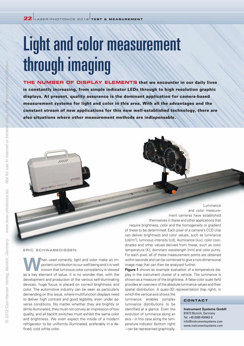
Luminance
and color measure-
ment cameras have established
themselves in these and other applications that
require brightness, color and the homogeneity or gradient
of these to be determined. Each pixel of a camera’s CCD chip
can deliver brightness and color values, such as luminance
[cd/m2], luminous intensity [cd], illuminance [lux], color coor-
dinates and other values derived from these, such as color
temperature [K], dominant wavelength [nm] and color purity.
For each pixel, all of these measurement points are obtained
within seconds and can be combined to give a two-dimensional
image map that can then be analyzed further.
Figure 1 shows an example evaluation of a temperature dis-
play in the instrument cluster of a vehicle. The luminance is
shown as a measure of the brightness. A false-color scale (left)
provides an overview of the absolute luminance values and their
spatial distribution. A quasi-3D representation (top right), in
which the vertical axis shows the
luminance, enables complex
luminance distributions to be
identified at a glance. Even the
evolution of luminance along an
axis – in this case along the tem-
perature indicator (bottom right)
– can be represented graphically.
22 l LASER+PHOTONICS 2 0 12 lTEST & MEASUREMENT
Light and color measurementthrough imagingTHE NUMBER OF DISPLAY ELEMENTS that we encounter in our daily lives
is constantly increasing, from simple indicator LEDs through to high resolution graphic
displays. At present, quality assurance is the dominant application for camera-based
measurement systems for light and color in this area. With all the advantages and the
constant stream of new applications for this now well-established technology, there are
also situations where other measurement methods are indispensable.
ER IC SCHWABEDISSEN
When used correctly, light and color make an im-
portant contribution to our well being and it is well
known that luminous color consistency is viewed
as a key element of value. It is no wonder that, with the
development and production of the various self-illuminating
devices, huge focus is placed on correct brightness and
color. The automotive industry can be seen as particularly
demanding on this issue, where multifunction displays need
to deliver high contrast and good legibility, even under ad-
verse conditions. No matter whether they are brightly or
dimly illuminated, they must not convey an impression of low
quality, and all backlit switches must exhibit the same color
and brightness. We even expect the inside of a modern
refrigerator to be uniformly illuminated, preferably in a de-
fined, cold white color.
Instrument Systems GmbH 81673 Munich, Germany
Tel. +49 (0)89 454943-0
www.instrumentsystems.com
CONTACT
22-25_LPX110096_inst sys_lay_LPex2012 ax 15.12.2011 16:22 Uhr Seite 22
© 2
012
Car
l Han
ser V
erla
g, M
unic
h, G
erm
any
w
ww
.lase
r-ph
oton
ics.
eu
Not
for u
se in
inte
rnet
or i
ntra
net s
ites.
Not
for e
lect
roni
c di
strib
utio
n.
Needless to say, these and many other evaluation methods
represent a major simplification compared to spatially selec-
tive measurement methods, and have helped camera-based
systems to become widespread in research depart-
ments, in quality assurance and in manufacturing.
Imaging photometry and colorimetry
Photometry involves evaluation of the energy or power
of light using what is known as the V(l) curve (Fig-ure 2) that describes the sensitivity of the human eye
in the wavelength range from 360 to 830 nm. It is used,
for example, to calculate the photometric luminance
value [cd/m2] from the radiance [W/m2 sr].
Thus, if we want to measure luminance with a camera
system, the object to be studied is reproduced on a
CCD image sensor using a high quality lens followed
by a V(l) filter. The signals of the individual pixels of the
image sensor then only have to be adjusted on a PC
according to a previously determined calibration.
Colorimetry, the quantitative description of color, is
very similar. ›CIE tristimulus‹ colorimetry is the most
widely-used system for color determination and is
based on the assumption that every color is a combi-
nation of the three primary colors red, green and blue.
The tristimulus system was established by the CIE
(International Lighting Commission) in 1931. The tri-
stimulus values X, Y, and Z are obtained by integrat-
ing the spectral radiation distribution S(l) over the three
eye sensitivity curves x(l), y(l) and z(l) (Figure 2) in
the wavelength range 360 to 830 nm. The tristimulus
values X, Y, and Z are then used to calculate the
widely used color coordinates x, y, and z.
If color coordinates and values derived from them, such
as the color temperature, are to be determined using
a camera system, at least three filters are required to
simulate the tristimulus functions x(l), y(l) and z(l).
As y(l) corresponds to V(l), photometric measure-
ments are also possible. However, the x(l) function is
normally captured using two separate filters, one fil-
ter for the blue component and one for red, which
results in a significant improvement in accuracy com-
pared to conventional color measurement equipment
with just three filters.
Figure 2 shows the variations of
actual spectral response functions
from the ideal CIE curves. These
variations are relatively significant
on the wings of the curves. Partic-
ularly with blue, red and white LEDs,
this results in major variations in the
photometric value determined and
the measured dominant wave-
length [1, 2]. Figure 3 illustrates
this using an error in the dominant
wavelength of different colored
LEDs determined using a typical
color measurement camera.
If samples with the same spectral
radiation are investigated repeat-
edly, for example in quality assur-
ance, the user can correct for this undesirable effect by ad-
justing the calibration in the relevant wavelength range. This
requires high precision measurement of the absolute value for
TEST & MEASUREMENT l LASER+PHOTONICS 2012 l23
1 Evaluating the luminance of a temperature display
2 Tristimulus functions x(l), y(l), z(l), as achieved with an ideal filter setand to CIE specifications; y(l) corresponds to V(l)
© LASER+PHOTONICS
3 Measurement error in the dominant wavelength of LEDs
© LASER+PHOTONICS
Wavelength (nm)
Dominant wavelength (nm)
Spe
ctra
l val
ue (r
el. u
nits
)V
aria
tion
err
or (n
m)
22-25_LPX110096_inst sys_lay_LPex2012 ax 15.12.2011 16:22 Uhr Seite 23
© 2
012
Car
l Han
ser V
erla
g, M
unic
h, G
erm
any
w
ww
.lase
r-ph
oton
ics.
eu
Not
for u
se in
inte
rnet
or i
ntra
net s
ites.
Not
for e
lect
roni
c di
strib
utio
n.
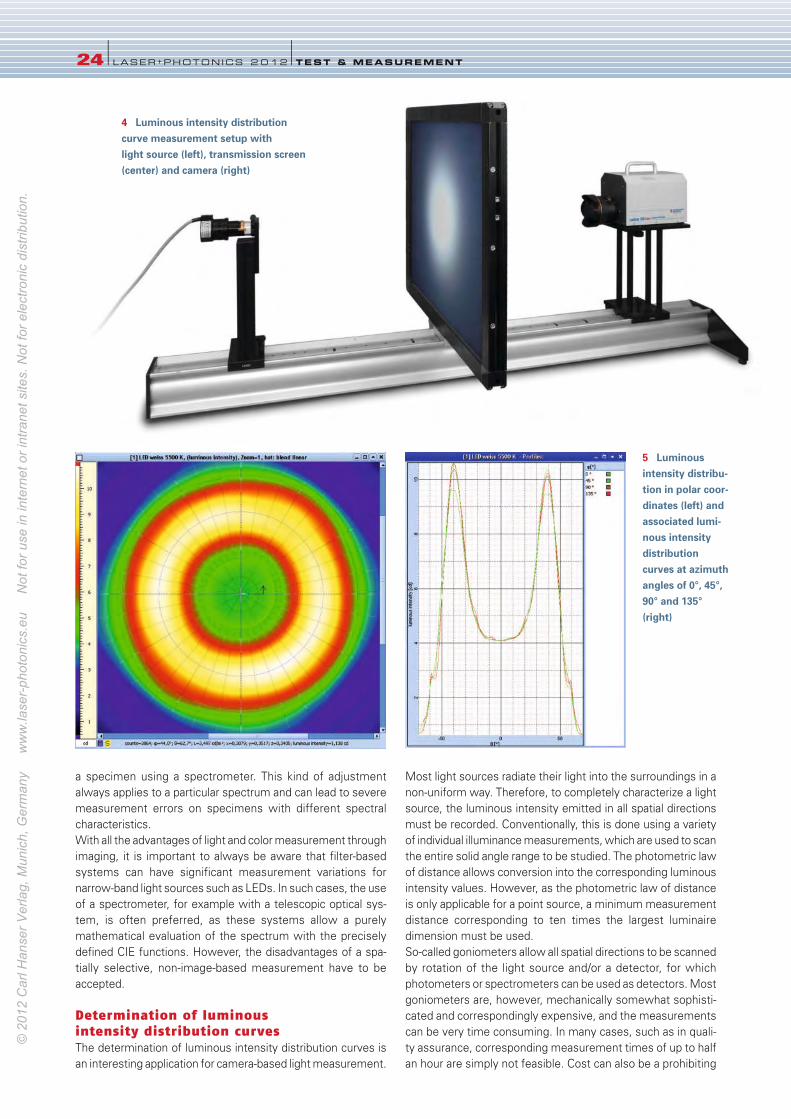
a specimen using a spectrometer. This kind of adjustment
always applies to a particular spectrum and can lead to severe
measurement errors on specimens with different spectral
characteristics.
With all the advantages of light and color measurement through
imaging, it is important to always be aware that filter-based
systems can have significant measurement variations for
narrow-band light sources such as LEDs. In such cases, the use
of a spectrometer, for example with a telescopic optical sys-
tem, is often preferred, as these systems allow a purely
mathematical evaluation of the spectrum with the precisely
defined CIE functions. However, the disadvantages of a spa-
tially selective, non-image-based measurement have to be
accepted.
Determination of luminous
intensity distribution curves
The determination of luminous intensity distribution curves is
an interesting application for camera-based light measurement.
Most light sources radiate their light into the surroundings in a
non-uniform way. Therefore, to completely characterize a light
source, the luminous intensity emitted in all spatial directions
must be recorded. Conventionally, this is done using a variety
of individual illuminance measurements, which are used to scan
the entire solid angle range to be studied. The photometric law
of distance allows conversion into the corresponding luminous
intensity values. However, as the photometric law of distance
is only applicable for a point source, a minimum measurement
distance corresponding to ten times the largest luminaire
dimension must be used.
So-called goniometers allow all spatial directions to be scanned
by rotation of the light source and/or a detector, for which
photometers or spectrometers can be used as detectors. Most
goniometers are, however, mechanically somewhat sophisti-
cated and correspondingly expensive, and the measurements
can be very time consuming. In many cases, such as in quali-
ty assurance, corresponding measurement times of up to half
an hour are simply not feasible. Cost can also be a prohibiting
24 l LASER+PHOTONICS 2 0 12 lTEST & MEASUREMENT
4 Luminous intensity distributioncurve measurement setup with light source (left), transmission screen(center) and camera (right)
5 Luminousintensity distribu-tion in polar coor-dinates (left) andassociated lumi-nous intensitydistributioncurves at azimuthangles of 0°, 45°,90° and 135°(right)
22-25_LPX110096_inst sys_lay_LPex2012 ax 15.12.2011 16:22 Uhr Seite 24
© 2
012
Car
l Han
ser V
erla
g, M
unic
h, G
erm
any
w
ww
.lase
r-ph
oton
ics.
eu
Not
for u
se in
inte
rnet
or i
ntra
net s
ites.
Not
for e
lect
roni
c di
strib
utio
n.
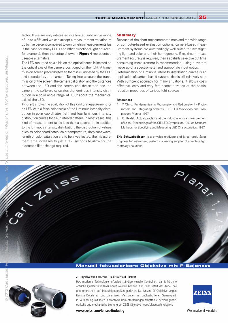
factor. If we are only interested in a limited solid angle range
of up to ±65° and we can accept a measurement variation of
up to five percent compared to goniometric measurements (as
is the case for many LEDs and other directional light sources,
for example), then the setup shown in Figure 4 represents a
useable alternative.
The LED mounted on a slide on the optical bench is located on
the optical axis of the camera positioned on the right. A trans-
mission screen placed between them is illuminated by the LED
and recorded by the camera. Taking into account the trans-
mission of the screen, the camera calibration and the distances
between the LED and the screen and the screen and the
camera, the software calculates the luminous intensity distri-
bution in a solid angle range of ±65° about the mechanical
axis of the LED.
Figure 5 shows the evaluation of this kind of measurement for
an LED with a false-color scale of the luminous intensity distri-
bution in polar coordinates (left) and four luminous intensity
distribution curves for a 45° interval pattern. In most cases, this
kind of measurement takes less than a second. If, in addition
to the luminous intensity distribution, the distribution of values
such as color coordinates, color temperature, dominant wave-
length or color saturation are to be investigated, the measure-
ment time increases to just a few seconds to allow for the
automatic filter change required.
Summary
Because of the short measurement times and the wide range
of computer-based evaluation options, camera-based meas-
urement systems are outstandingly well suited for investigat-
ing light and color and their homogeneity. If maximum meas-
urement accuracy is required, then a spatially selective but time
consuming measurement is recommended, using a system
made up of a spectrometer and appropriate input optics.
Determination of luminous intensity distribution curves is an
application of camera-based systems that is still relatively rare.
With sufficient accuracy for many situations, it allows cost-
effective, easy and very fast characterization of the spatial
radiation properties of various light sources.
References 1 Y. Ohno: ‘Fundamentals in Photometry and Radiometry II – Photo-
meters and Integrating Spheres’, CIE LED Workshop and Sym-
posium, Vienna, 1997
2 G. Heidel: ‘Actual problems at the industrial optical measurement
of Leds’, Proceedings of the CIE LED Symposium 1997 on Standard
Methods for Specifying and Measuring LED Characteristics, 1997
Eric Schwabedissen is a physics graduate and is currently Sales
Engineer for Instrument Systems, a leading supplier of complete light
metrology solutions.
TEST & MEASUREMENT l LASER+PHOTONICS 2012 l25
22-25_LPX110096_inst sys_lay_LPex2012 ax 15.12.2011 16:22 Uhr Seite 25
© 2
012
Car
l Han
ser V
erla
g, M
unic
h, G
erm
any
w
ww
.lase
r-ph
oton
ics.
eu
Not
for u
se in
inte
rnet
or i
ntra
net s
ites.
Not
for e
lect
roni
c di
strib
utio
n.
26 l LASER+PHOTONICS 2 0 12 lTEST & MEASUREMENT
Scanning Fizeau interferometryDETERMINISTIC CORRECTION OF PRECISION ASPHERES. Optical systems, such as photographic lenses, projectors, cameras, binoculars and laser
systems are made up of a variety of individual optical elements. In addition to the
standard planar and spherical optical components, such as prisms, filters and lenses,
these also increasingly include aspherical lenses.
TORSTEN GLASCHKE
SVEN R. K IONTKE
T he advantage of aspheres lies in their greater design
flexibility and the possibility of achieving identical or
even better imaging qualities with fewer optical com-
ponents (Figure 1). This enables lighter and more compact
complete systems to be designed and makes them easier
to produce, all resulting in considerable cost savings.
Local surface correction for
high precision surfaces
The quality of optical surfaces is typically expressed as the vari-
ation of the actual shape from the specified shape, for exam-
ple using the PV (peak to valley) value. These are measured
by interferometric comparison with a reference surface that
matches the exact intended shape. To achieve surface quali-
ties better than l /10 (with wavelength l being typically
633 nm), the measured result is used to determine local
correction. Relevant technologies include ion beam figuring,
fluid jet polishing and magnetorheological finishing (MRF).
This correction process
places high demands on the
measurement technology as
every measuring error or
data artifact has a negative
influence on the result and,
in the worst case, leads to
errors being incorporated
into the surface. Of course,
they are then no longer iden-
tified as errors by the meas-
urement system used.
Suppression of coherent artifacts
Interferometers that are able to suppress measurement artifacts
have been proven to be appropriate metrology systems for this
kind of correction method, also because they provide a high
lateral resolution and feature a very low system noise. This
approach is already widespread for planar and spherical sur-
faces, although aspheres still present a major challenge as there
are no suitable surfaces that can act as an interferometric ref-
erence surface. Current measurement methods therefore use
standard interferometers with spherical or planar reference
optics and generate the measurement wavefront by using a
computer generated hologram or a null optic. Nevertheless, a
wavefront accuracy of l/10 is difficult to achieve with these
optics, and the manufacturing process taking several weeks is
a barrier to rapid product launches.
Another more flexible method is to measure smaller sub-aper-
tures and then combine the overlapping individual results to
give an overall measurement (stitching). The disadvantages
when using a large number of sub-apertures are extremely long
measurement times and problems in detecting long period
surface errors caused by the measurement principle.
The sub-apertures are selected in such a way that the high fringe
resolution of the interferometer in the current field of
view can be utilized to perform a measurement. For
milder aspheres, measurements can also be made
directly against a reference sphere.
Fizeau common path
measurement
principle
The crucial
advantage of
the Fizeau
ZygoLOT GmbH 64293 Darmstadt, Germany
Tel. +49 (0)6151 8806-27
www.zygolot.de
asphericon GmbH 07747 Jena, Germany
Tel. +49 (0)3641 3100500
www.asphericon.com
CONTACT
1 Aspherical glass lenses
26-29_LPX110097_zygoLOT_LPex2012 ax 15.12.2011 16:26 Uhr Seite 26
© 2
012
Car
l Han
ser V
erla
g, M
unic
h, G
erm
any
w
ww
.lase
r-ph
oton
ics.
eu
Not
for u
se in
inte
rnet
or i
ntra
net s
ites.
Not
for e
lect
roni
c di
strib
utio
n.
interferometers used is their so-called ›common path‹ con-
struction. The interferometric beam splitter and the reference
surface are combined in a single component at the output aper-
ture, which means that if there is a perfect match between the
reference surface and the measurement surface, the path of
both wavefronts in the interferometer is identical and no
›retrace‹ errors occur. This match is achieved by nulling fringes
during alignment of the measurement object. The key require-
ment is that the surface to be measured must have exactly the
same shape as the reference surface. However, when meas-
uring a complete asphere or when using sub-apertures, this is
obviously not possible.
It is thus necessary to use calibration methods to correct for
errors, but even still, with increasing aspherical variation from
the ›best fit‹ sphere, the measurement uncertainty increases.
Scanning Fizeau interferometry
To assist in manufacturing rotationally symmetric precision
aspheres, Zygo has developed a measurement method that
avoids or minimizes these sources of errors through the
approach used. Scanning Fizeau interferometry is based
exclusively on interferometric length measurement (Figure 2)
[1]. The method utilizes the fact that, in principle, a rotational-
ly symmetrical asphere is nothing other than a surface made
up of a large number of circular rings (zones) with different
radii. Each individual circular ring can be measured against a
spherical reference surface in the common path approach.
Starting at the outer edge of the lens, each zone is successively
measured and used to determine the surface coordinates of
the asphere. The number of zones required essentially depends
on the aspherical variation and determines the total measure-
ment time (typically between five and ten minutes).
The starting point for every measurement process is the
specific asphere formula, which is entered into the software
along with the required test diameter. This determines the
measurability of the lens based on mechanical and optical con-
ditions, and thus determines the measurement sequence.
A crucial advantage of the method is direct measurement in
the object coordinates of the asphere to be tested, so there is
no need for a conversion between the detector and object
coordinates. This means that image field distortion and magni-
fication of the instrument’s optical system have no influence
on the measurement accuracy.
In contrast to alternative measurement methods, as discussed
above, precise measurement of the vertex radius of
the asphere (R0) is possible, as is the
determination of coma error in
the specimen.
Hamamatsu Photonics Deutschland GmbHArzbergerstr.10 · D-82211 Herrsching
Phone: +49 8152 375 100 · Fax: +49 8152 375 111Email: [email protected] · http://www.hamamatsu.de
MPPC Array Types forPET /MR Imaging
New range of high sensitivity MPPC arrays and modules featuring good space and time resolution
in a compact package.
26-29_LPX110097_zygoLOT_LPex2012 ax 15.12.2011 16:26 Uhr Seite 27
© 2
012
Car
l Han
ser V
erla
g, M
unic
h, G
erm
any
w
ww
.lase
r-ph
oton
ics.
eu
Not
for u
se in
inte
rnet
or i
ntra
net s
ites.
Not
for e
lect
roni
c di
strib
utio
n.
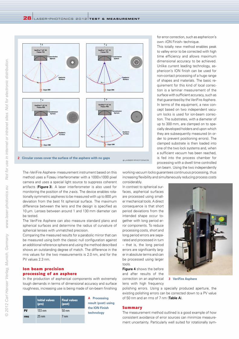
The ›VeriFire Asphere‹ measurement instrument based on this
method uses a Fizeau interferometer with a 1000x1000 pixel
camera and uses a special light source to suppress coherent
artifacts (Figure 3). A laser interferometer is also used for
monitoring the position of the z-axis. The device enables rota-
tionally symmetric aspheres to be measured with up to 800 µm
deviation from the best fit spherical surface. The maximum
difference between the lens and the design is specified as
10 µm. Lenses between around 1 and 130 mm diameter can
be tested.
The VeriFire Asphere can also measure standard plano and
spherical surfaces and determine the radius of curvature of
spherical lenses with unmatched precision.
Comparing the measured results for a parabolic mirror that can
be measured using both the classic null configuration against
an additional reference sphere and using the method described
shows an outstanding degree of match. The difference in the
rms values for the two measurements is 2.0 nm, and for the
PV values 2.3 nm.
Ion beam precision
processing of an asphere
In the production of aspherical components with extremely
tough demands in terms of dimensional accuracy and surface
roughness, increasing use is being made of ion-beam finishing
for error correction, such as asphericon’s
own ›ION Finish‹ technique.
This totally new method enables peak
to valley error to be corrected with high
time efficiency and allows maximum
dimensional accuracy to be achieved.
Unlike current leading technology, as-
phericon’s ION finish can be used for
non-contact processing of a huge range
of shapes and materials. The basic re-
quirement for this kind of local correc-
tion is a laminar measurement of the
surface with sufficient accuracy, such as
that guaranteed by the VeriFire Asphere.
In terms of the equipment, a new con-
cept based on two independent vacu-
um locks is used for ion-beam correc-
tion. The substrates, with a diameter of
up to 300 mm, are clamped on to spe-
cially developed holders and upon which
they are subsequently measured (in or-
der to prevent positioning errors). The
clamped substrate is then loaded into
one of the two lock systems and, when
a sufficient vacuum has been reached,
is fed into the process chamber for
processing with a dwell time controlled
ion beam. Using the two independently
working vacuum locks guarantees continuous processing, thus
increasing flexibility and simultaneously reducing process costs
considerably.
In contrast to spherical sur-
faces, aspherical surfaces
are processed using small-
er mechanical tools. A direct
consequence is that short
period deviations from the
intended shape occur to-
gether with long period er-
ror components. To reduce
processing costs, short and
long period errors are sepa-
rated and processed in turn
– that is, the long period
errors are significantly larg-
er in absolute terms and can
be processed using larger
tools.
Figure 4 shows the before
and after results of the
correction on an aspherical
lens with high frequency
polishing errors. Using a specially produced aperture, the
existing polishing errors can be corrected down to a PV value
of 50 nm and an rms of 7 nm (Table A).
Summary
The measurement method outlined is a good example of how
consistent avoidance of error sources can minimize measure-
ment uncertainty. Particularly well suited for rotationally sym-
28 l LASER+PHOTONICS 2 0 12 lTEST & MEASUREMENT
Initial values(pre)
Final values(post)
PV 133 nm 50 nm
rms 25 nm 7 nm
A Processingresult (post) usingthe ION Finishtechnology
2 Circular zones cover the surface of the asphere with no gaps © LASER+PHOTONICS
3 VeriFire Asphere
26-29_LPX110097_zygoLOT_LPex2012 ax 15.12.2011 16:27 Uhr Seite 28
© 2
012
Car
l Han
ser V
erla
g, M
unic
h, G
erm
any
w
ww
.lase
r-ph
oton
ics.
eu
Not
for u
se in
inte
rnet
or i
ntra
net s
ites.
Not
for e
lect
roni
c di
strib
utio
n.
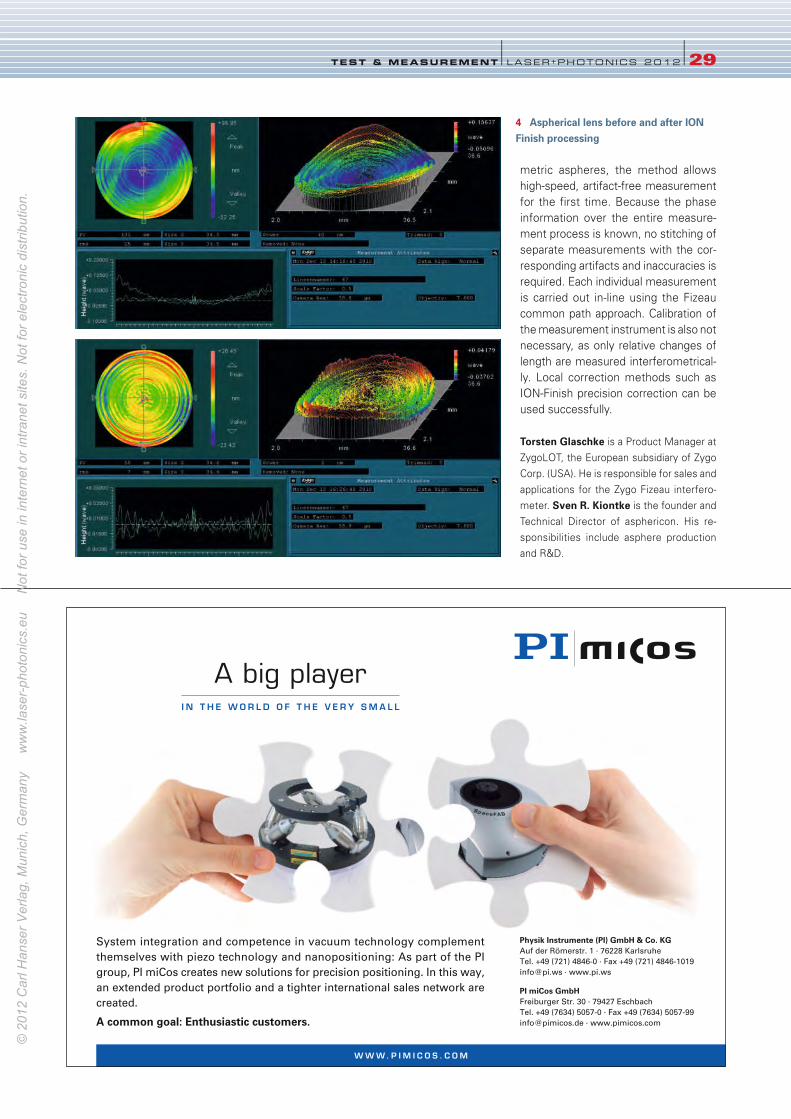
metric aspheres, the method allows
high-speed, artifact-free measurement
for the first time. Because the phase
information over the entire measure-
ment process is known, no stitching of
separate measurements with the cor-
responding artifacts and inaccuracies is
required. Each individual measurement
is carried out in-line using the Fizeau
common path approach. Calibration of
the measurement instrument is also not
necessary, as only relative changes of
length are measured interferometrical-
ly. Local correction methods such as
ION-Finish precision correction can be
used successfully.
Torsten Glaschke is a Product Manager at
ZygoLOT, the European subsidiary of Zygo
Corp. (USA). He is responsible for sales and
applications for the Zygo Fizeau interfero-
meter. Sven R. Kiontke is the founder and
Technical Director of asphericon. His re-
sponsibilities include asphere production
and R&D.
TEST & MEASUREMENT l LASER+PHOTONICS 2012 l29
4 Aspherical lens before and after IONFinish processing
System integration and competence in vacuum technology complement
themselves with piezo technology and nanopositioning: As part of the PI
group, PI miCos creates new solutions for precision positioning. In this way,
an extended product portfolio and a tighter international sales network are
created.
A common goal: Enthusiastic customers.
Physik Instrumente (PI) GmbH & Co. KGAuf der Römerstr. 1 · 76228 Karlsruhe
Tel. +49 (721) 4846-0 · Fax +49 (721) 4846-1019
[email protected] · www.pi.ws
PI miCos GmbHFreiburger Str. 30 · 79427 Eschbach
Tel. +49 (7634) 5057-0 · Fax +49 (7634) 5057-99
[email protected] · www.pimicos.com
A big playerI N T H E W O R L D O F T H E V E R Y S M A L L
W W W. P I M I C O S . C O M
pi_111095_uebernahme_175x122_en.indd 1 24.11.11 16:32
26-29_LPX110097_zygoLOT_LPex2012 ax 15.12.2011 16:27 Uhr Seite 29
© 2
012
Car
l Han
ser V
erla
g, M
unic
h, G
erm
any
w
ww
.lase
r-ph
oton
ics.
eu
Not
for u
se in
inte
rnet
or i
ntra
net s
ites.
Not
for e
lect
roni
c di
strib
utio
n.
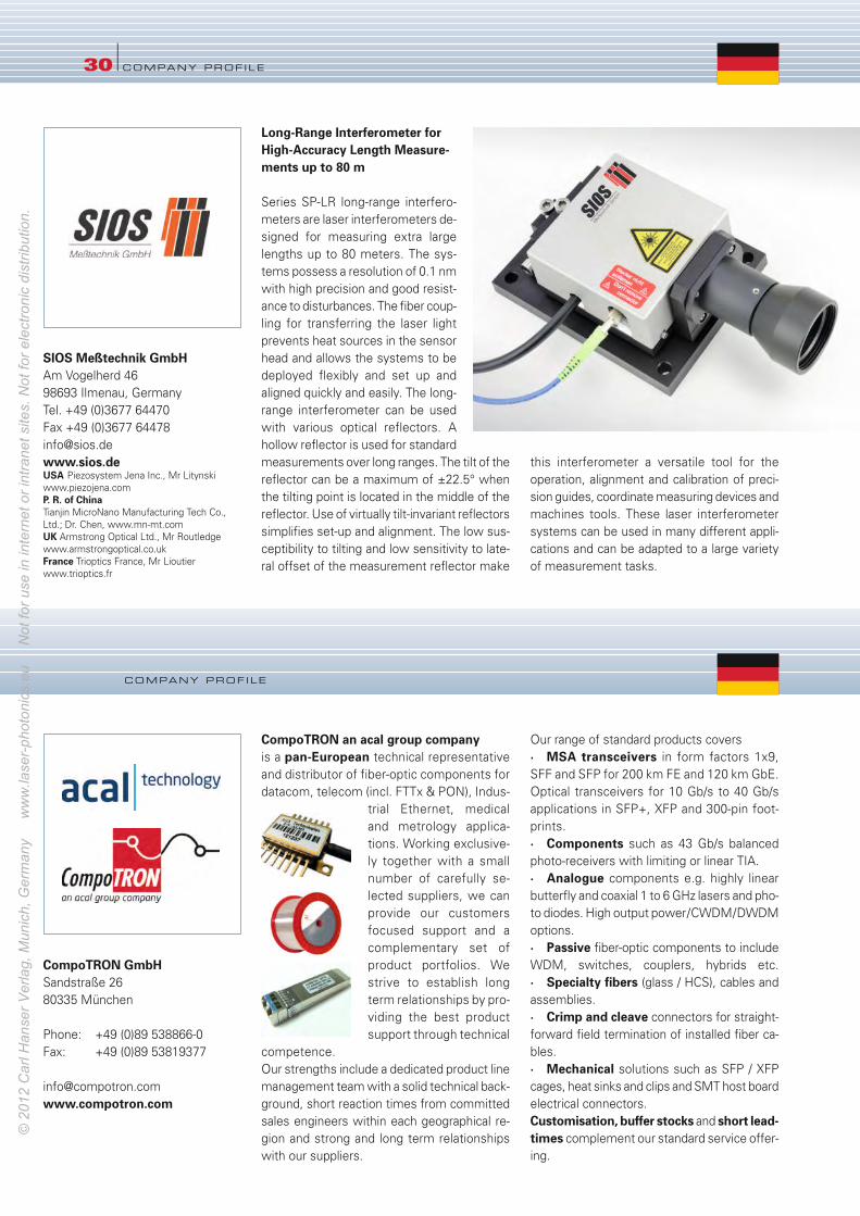
30 lCOMPANY PROF ILE
COMPANY PROF ILE
SIOS Meßtechnik GmbHAm Vogelherd 46
98693 Ilmenau, Germany
Tel. +49 (0)3677 64470
Fax +49 (0)3677 64478
www.sios.deUSA Piezosystem Jena Inc., Mr Litynski
www.piezojena.com
P. R. of ChinaTianjin MicroNano Manufacturing Tech Co.,
Ltd.; Dr. Chen, www.mn-mt.com
UK Armstrong Optical Ltd., Mr Routledge
www.armstrongoptical.co.uk
France Trioptics France, Mr Lioutier
www.trioptics.fr
Long-Range Interferometer forHigh-Accuracy Length Measure-ments up to 80 m
Series SP-LR long-range interfero-
meters are laser interferometers de-
signed for measuring extra large
lengths up to 80 meters. The sys-
tems possess a resolution of 0.1 nm
with high precision and good resist-
ance to disturbances. The fiber coup-
ling for transferring the laser light
prevents heat sources in the sensor
head and allows the systems to be
deployed flexibly and set up and
aligned quickly and easily. The long-
range interferometer can be used
with various optical reflectors. A
hollow reflector is used for standard
measurements over long ranges. The tilt of the
reflector can be a maximum of ±22.5° when
the tilting point is located in the middle of the
reflector. Use of virtually tilt-invariant reflectors
simplifies set-up and alignment. The low sus-
ceptibility to tilting and low sensitivity to late-
ral offset of the measurement reflector make
this interferometer a versatile tool for the
operation, alignment and calibration of preci-
sion guides, coordinate measuring devices and
machines tools. These laser interferometer
systems can be used in many different appli-
cations and can be adapted to a large variety
of measurement tasks.
CompoTRON GmbHSandstraße 26
80335 München
Phone: +49 (0)89 538866-0
Fax: +49 (0)89 53819377
www.compotron.com
CompoTRON an acal group companyis a pan-European technical representative
and distributor of fiber-optic components for
datacom, telecom (incl. FTTx & PON), Indus-
trial Ethernet, medical
and metrology applica-
tions. Working exclusive-
ly together with a small
number of carefully se-
lected suppliers, we can
provide our customers
focused support and a
complementary set of
product portfolios. We
strive to establish long
term relationships by pro-
viding the best product
support through technical
competence.
Our strengths include a dedicated product line
management team with a solid technical back-
ground, short reaction times from committed
sales engineers within each geographical re-
gion and strong and long term relationships
with our suppliers.
Our range of standard products covers
· MSA transceivers in form factors 1x9,
SFF and SFP for 200 km FE and 120 km GbE.
Optical transceivers for 10 Gb/s to 40 Gb/s
applications in SFP+, XFP and 300-pin foot-
prints.
· Components such as 43 Gb/s balanced
photo-receivers with limiting or linear TIA.
· Analogue components e.g. highly linear
butterfly and coaxial 1 to 6 GHz lasers and pho-
to diodes. High output power/CWDM/DWDM
options.
· Passive fiber-optic components to include
WDM, switches, couplers, hybrids etc.
· Specialty fibers (glass / HCS), cables and
assemblies.
· Crimp and cleave connectors for straight-
forward field termination of installed fiber ca-
bles.
· Mechanical solutions such as SFP / XFP
cages, heat sinks and clips and SMT host board
electrical connectors.
Customisation, buffer stocks and short lead-times complement our standard service offer-
ing.
_FP_LPex2012 14.12.2011 15:44 Uhr Seite 30
© 2
012
Car
l Han
ser V
erla
g, M
unic
h, G
erm
any
w
ww
.lase
r-ph
oton
ics.
eu
Not
for u
se in
inte
rnet
or i
ntra
net s
ites.
Not
for e
lect
roni
c di
strib
utio
n.
COMPANY PROF ILE l31
www.jenoptik.com/lm
Europe: +49 3641 65-4300
Russia: +7 812 610 50-50
China: +86 21 3825 2380-268
Japan: +81 45 345-0003
Korea: +82 31 646-4020
USA: +1 248 446-9540
www.jenoptik.com/os
Europe: +49 3641 65-2276
Israel: +972 8 930-3501
China: +86 186 1655 1890
Japan: +81 45 345-0002
Korea: +82 10 3753-2503
USA: +1 561 881 7400
Jenoptik’s Lasers & Material Processing di-
vision has control of the entire value-added
chain of laser material processing. Jenoptik is
a leading provider across this value chain, from
laser components through laser systems to
turnkey laser processing tools.
In the area of lasers, Jenoptik specializes in
high-quality semiconductor materials and re-
liable diode lasers as well as innovative solid-
state lasers, for example disk and fiber lasers.
Jenoptik is acknowledged worldwide as a
leader in quality for high-power diode lasers.
These laser sources are developed as compo-
nents and systems and integrated into com-
plete systems for usage in many applications.
In the area of laser processing systems,
Jenoptik supplies laser systems and turn-
key laser processing tools which are integrat-
ed into production facilities for our customers
as part of their process optimization and
automation. These systems enable our cus-
tomers to work with several materials with
maximum efficiency, precision and safety.
Our Key Markets are:· Automotive / machine construction /
metal processing industry
· Photovoltaics / semiconductor industry /
electronics
· Medical technology
· Show & entertainment
· Defense & security technology
JENOPTIK I Lasers & Material ProcessingLight – Power to Work with
JENOPTIK I Optical SystemsIntegrating Opto-electronic Technologies
Through its Optical Systems division, the
Jenoptik Group delivers world class precision
optics and systems designed and manufac-
tured to the highest quality standards.
Besides offering customized systems, mod-
ules and assemblies, the Optical Systems di-
vision is a development and production part-
ner for optical, microoptical and coated optical
components - made of optical glasses, IR
materials as well as polymers.
It possesses outstanding expertise in the
development and manufacture of optics and
microoptics for beam shaping used in the semi-
conductor industry and laser material process-
ing.
The product portfolio also includes optical and
opto-electronic systems and components for
applications in defense & security, health care
& life science, digital imaging, machine vision
as well as lighting.
Our Key Markets are:· Semiconductor & flat panel display
equipment
· Laser material processing
· Defense & security technology
· Medical technology
· Digital imaging
· Automotive
_FP_LPex2012 14.12.2011 15:44 Uhr Seite 31
© 2
012
Car
l Han
ser V
erla
g, M
unic
h, G
erm
any
w
ww
.lase
r-ph
oton
ics.
eu
Not
for u
se in
inte
rnet
or i
ntra
net s
ites.
Not
for e
lect
roni
c di
strib
utio
n.
32 lCOMPANY PROF ILE
COMPANY PROF ILE
MAZeT GmbHGöschwitzer Straße 32
D-07745 JENA, GERMANY
Phone: +49 (0)3641 2809-0
Fax: +49 (0)3641 2809-12
www.mazet.de
MAZeT GmbH – ElectronicDesign & Manufacturing Services
MAZeT GmbH is an electronics design & man-
ufacturing services provider, which is special-
ized in the market segment of medical elec-
tronics, automation technology and industrial
electronics with customized, embedded com-
puting solutions and mixed signal ASIC/FPGA
design services. MAZeT provides its own prod-
ucts and solutions for applications of spectral
and color sensor technology. MAZeT is certi-
fied according to ISO 9001:2008.
The business concept of MAZeT GmbH has
the goal of providing comprehensive service
from the product idea of the customer to the
delivery of customized electronics and their
maintenance during the complete product life
cycle.
MAZeT GmbH has an experienced engineer-
ing staff for developing FPGAs with substan-
tial requirements for data throughput (e.g., im-
age processing), embedded computing mod-
ules (Power PC, Intel) for medical equipment
and measuring equipment used outdoors, as
well as mixed signal ASICs for processing sen-
sor signals in industrial electronics. Develop-
ing firmware and customized application soft-
ware round out the scope of services offered
by MAZeT GmbH.
The development and production of electron-
ics for medical equipment is becoming increas-
ingly important in the market orientation of
MAZeT GmbH. MAZeT is regularly and increas-
ingly required to depict partial processes con-
forming to the DIN EN ISO 13485 standard
in projects for medical equipment. There are
currently activities for checking the on-going
process and the introduction of risk manage-
ment according to DIN EN ISO 14971. The goal
of the activities is to obtain the DIN ISO 13485
in 2012 certificate.
FRAMOS GmbHZugspitzstrasse 5 C
82049 Pullach/Munich, Germany
Phone +49 (0) 89 710667-0
Fax +49 (0) 89 710667-66
eMail [email protected]
www.framos.de
FRAMOS Electronics Ltd., UKwww.framos.co.uk
FRAMOS Italia srl, Italywww.framos.it
FRAMOS France, Francewww.framos.fr
FRAMOS has been active in the area of indus-
trial image processing for the last 30 years and
as an innovative partner provides a broad range
of high-quality components and services. Along
with offering image components such as sen-
sors, companion chips, camera modules, cam-
eras and accessories, we provide a real vari-
ety of development support services for cam-
era manufacturers and users.
FRAMOS Imaging ComponentsSells our partner companies’ image process-
ing components and systems across the globe.
In our component portfolio, we focus on the
areas of machine vision, medical, traffic and
security and provide you with every possible
component, from sensors to the GigE inter-
face, tailored to your needs.
FRAMOS Engineering Services You have an idea for a camera or an image pro-
cessing system? Your prototype needs to be
developed? Or you’re not happy because the
design is finished but it didn't turn out as you
had hoped? We will support you throughout
the whole value chain of your image process-
ing system. We consider the whole surround-
ing architecture (optics, lighting, mechanics,
server infrastructure, data editing etc.).
FRAMOS Solutions FRAMOS Solutions works in linking our expert-
ise for system integrators to camera users.
Specialist engineers will support you in imple-
menting your ideas and projects, comprehen-
sively and competently. If you want to use an
image processing system, we will help you to
select the best possible combination of all com-
ponents such as cameras, lenses and lighting,
as well as the right software.
_FP_LPex2012 14.12.2011 15:44 Uhr Seite 32
© 2
012
Car
l Han
ser V
erla
g, M
unic
h, G
erm
any
w
ww
.lase
r-ph
oton
ics.
eu
Not
for u
se in
inte
rnet
or i
ntra
net s
ites.
Not
for e
lect
roni
c di
strib
utio
n.

COMPANY PROF ILE l33
Optics Balzers AGNeugrüt 35
9496 Balzers, Liechtenstein
Phone +423 388 9200
Fax +423 388 9390
www.opticsbalzers.com
Optics Balzers Jena GmbHCarl-Zeiss-Promenade 10
07745 Jena, Germany
Germany+49 (0)6196 999 4144
France+33 699 5562 83
Switzerland, Austria+423 388 9216
USA+1 720 974 5927
Solutions from OpticsBalzersOptics Balzers is the leading European com-
petence center for optical coatings and com-
ponents, and worldwide the preferred and in-
dependent partner for the photonics industry.
The company possesses a broad and in-depth
know-how in optical thin-film coating process-
es, complemented by sophisticated pattern-
ing, glass bonding and sealing, and further
processing capabilities necessary for produc-
ing optical thin-film coated components up to
optical subassemblies. Highly experienced and
skilled development and engineering teams
closely collaborate with customers to develop
innovative solutions meeting their specific
and nique requirements and design robust
processes to manufacture the customer spe-
cific components. The combination of these
capabilities and skills places Optics Balzers
at the forefront of markets in the photonics
industry such as Sensors & Imaging, Biopho-
tonics, Space & Defence, Lighting & Projec-
tion and Industrial Applications.
With over 65 years of experience in optical
coating technology, Optics Balzers possesses
profound knowledge in optical component
manufacturing. Customers benefit from state-
of-the-art vacuum-deposition technologies, var-
ious adapted patterning, bonding and glass
processing technologies operated in modern
facilities with clean room environments.
With its acquisition of mso jena Mikroschicht-
optik GmbH in Jena, Germany, Optics Balzers
is expanding its competencies and manufac-
turing technologies into a unique portfolio, gen-
erating added value for customers.
Optics Balzers’ continuous innovation, quality
improvements, additions of expertise and
production sites in Liechtenstein and the EU,
will continue to support customers’ novel
product development efforts with Optics
Balzers as a trusted, reliable, and innovative
partner.
Examples of Optical Coatings &Components· Anti-reflection coatings
· Matched ITO coatings
· Opaque chrome coatings
· Bandpass filters
· NIR filters
· Notch filters
· UV filters
· Filter Arrays
· Filter-on-chip
Sealing Technologies· Gelot™ solderable coatings
· B-stage Epoxy
Patterning· Photolithography
· Laser Ablation
· Masked coatings
_FP_LPex2012 14.12.2011 15:44 Uhr Seite 33
© 2
012
Car
l Han
ser V
erla
g, M
unic
h, G
erm
any
w
ww
.lase
r-ph
oton
ics.
eu
Not
for u
se in
inte
rnet
or i
ntra
net s
ites.
Not
for e
lect
roni
c di
strib
utio
n.
Made to measure Customized spectrometers. Brand new
compact subsystems extend tec5’s range
of premium UV/VIS/NIR spectroscopy
products. The spectrometer modules are
customized with electronic boards and
other components and supplied as ready
to use solutions. The measurement
results can be transferred to a host
computer via Ethernet or USB as spectral
data or directly evaluated by the internal
microcontroller (embedded processing).
The individually tailored design, range of
functions and external interfaces ensure
reliable and time-saving integration of the
units, fully assembled and tested to cus-
tomer specifications. If servicing is need-
ed, the subsystem can be exchanged
quickly and easily. Production, spare parts
storage and logistics are provided by tec5
as customer services.
www.tec5.com
USB stick ...... spectrometer. RGB Lasersysteme’s
›Qstick‹ represents the ultimate in spec-
trometer miniaturization: a complete
spectrometer in a small USB stick design,
offering a resolution of 1.0 nm across the
full visible spectrum. It includes the
advanced spectroscopy software ›Waves‹
that offers sophisticated algo-
rithms for data acquisi-
tion and evalua-
tion and provides
these features
through a clear and
simple user interface. The Qstick is an
ideal instrument for scientific field meas-
urements and light analysis.
www.rgb-laser.com
Layer analysis THz-TDS analysis software. Menlo
Systems is introducing ›TeraLyzer‹, a new
terahertz data evaluation software de-
veloped by LyTera, enabling advanced
data analysis and THz time-domain spec-
troscopy (TDS) experimentsl. Menlo
presents TeraLyzer as a first-of-its-kind
solution for the extraction of sample
thickness, enabling the investigation of
sub-100 µm samples without the need
for a differential measuring setup. At the
same time, complex THz material
parameters of a wide variety of sub-
stances can be determined. As an option,
the TeraLyzer software is also able to
analyze multilayer systems in a
standard THz-TDS setup, thus
opening up the door for a whole
new range of experiments. Menlo
Systems’ experience in fs-laser based
THz-TDS laboratory systems in conjunc-
tion with LyTera’s background in the THz
field offer a sound platform for customer
specific applications.
www.menlosystems.com
34 l LASER+PHOTONICS 2 0 12 lPRODUCT MARKETPLACE
your partner in ultrafast
APE Angewandte Physik & Elektronik GmbHPlauener Str. 163 - 165 | 13053 Berlin | Germany
www.ape-berlin.com
UItrafast Pulse Diagnostics
Wavelength Conversion
Pulse Management
Acousto-optics
Autocorrelators|Spiders
OPOs|Harmonics Generators
Pulse Compressors|Cavity Dumpers|Pulse Pickers
AOM|DFD
34-35_produkte_LPex2012_x 15.12.2011 16:29 Uhr Seite 34
© 2
012
Car
l Han
ser V
erla
g, M
unic
h, G
erm
any
w
ww
.lase
r-ph
oton
ics.
eu
Not
for u
se in
inte
rnet
or i
ntra
net s
ites.
Not
for e
lect
roni
c di
strib
utio
n.

LED inspection... with five channels. Micro-Epsilon of-
fers their new ›colorControl MFA-5‹ for
the inspection of LEDs, starting with a
basic version that offers five measuring
channels. This simplifies the inspection
of LEDs for function, contrast and lumi-
nosity. The MFA-5 is very compact and
can verify up to five LEDs simultaneous-
ly. The measuring system can be ex-
tended in a modular fashion by adding
extra MFA-E modules in batches of five
channels. The light from the target object
is transmitted to the inspection system
via a flexible, 2 mm diameter, plastic
optical fiber and is therefore evaluated
dynamically using a color sensor for color
and intensity. The color value, which is
evaluated within just a few milliseconds,
is output as RGB-, HIS or CIE values and
then transmitted via USB or RS232 in-
terface at a rate of between 9600 and
115 200 baud to a higher level inspection
or evaluation system for further pro-
cessing. In order to ensure a wide meas-
urement range for intensity (illumination),
the sensitivity of the sensor can be ad-
justed by using two different modes
(High Sensitivity Mode and Low Sensi-
tivity Mode) to eleven settings. Due to
these settings, it is possible to identify
LED colors up to ± 4 nm. A test software
to install the MFA-5 system is included
in the scope of delivery.
www.micro-epsilon.de
Compact, preciseLaser surface velocimeter. The new
compact LSV-2000 laser surface ve-
locimeter from Polytec can detect the
direction of movement and provide pre-
cise measurements when stationary, al-
lowing production processes to be fully
optimized. Measurement field depths and
speed ranges are independent of the
measurement distance. This extends the
range of possible applications, particular-
ly where short distances are involved,
such as variations in material thickness or
pipe diameter. Due to its compactness,
the LSV-2000 is suitable for installation in
tight spaces, such as in thickness
micrometers for rolling mills. For applica-
tions in harsh and hot environments, a
stable protective enclosure with water
cooling is available, while optional air
purge units ensure the laser has a clear
view in dusty surroundings. Laser Surface
Velocimeters allow users to reliably re-
duce waste in processes by reliably and
accurately measuring lengths. The speed
is measured directly on the material
without contact, thus reflecting the
actual material speed without slippage
problems. This enables the implementa-
tion of reliable control processes, such as
mass flow control.
www.velocimeter.de
Randomness at high bit ratesQuantum random number generator.At Photonics West, PicoQuant will un-
veil their photonic quantum random
number generator ›PQRNG 150‹, which
they claim to be the fastest system of
its kind commercially available today. The
PQRNG provides turn-key usability, a
high bit rate of up to 150 Mbits/s,deliv-
ered over USB, with long term statisti-
cal data quality. This high speed was
achieved by exploiting the most recent
photon timing instrumentation and state-
of-the-art data processing in hardware.
www.piqoquant.com
from 512 to 12 000 pixels
SK 9170: Gray Scale Line Signal – 0
SK 9170: Gray Scale Line Signal – 1
255
255
00
00
ZOOM
ZOOM
MicrosoftWindows xpProfessional
®
®
Modular interface concept:
Line Scan Camerasfor Research and Machine Vision.
Color, monochrome, or sensors.Catalog download:
www.SuKHamburg.de/linescanMad
e in G
erman
y
Laser Line, Micro Focus,Laser Pattern Generators
Made i
n Germ
anyWavelength 405 - 2050 nm
For Research and Machine Vision. Catalog download: www.SuKHamburg.de/laserlines
Depth of Focus:Plots of power density vs. working distance
100%
50%
0%0 0.75 1.5 2.25 mm
8
80 μm
160 μm 240 μm
Pow
er D
ensi
ty
Distance A
Line Width2
μm
Laser Micro Line Generatorsfor full power density in focus
20%
10%
0%0 0.75 1.5 2.25 mm
40 μm
40 μm
42 μm
47μm
Pow
er D
ensi
ty
Distance A
Line Width 2
Laser Macro Line Generatorsfor extended depth of focus
color monochrome1.0
0.0400 600 800 1000
Spectralrange
Spectralrange
Analog: RS422
Digital: LVDS
USB 2.0TM
Alfred-Wegener-Institute for Polar and Maritim Research
Innovative investigation of polar ice cores
LASM - Large AreaScan Macroscope
Analysis of grain bounda -ries and gas enclosures
Line Scan Camera with Dark-field Illumination
Applications
WAFER INSPECTION
Detection of diffuse reflectingscratches and particles downto the sub-micrometer range.
Application3D Profiling and Process Control
OEM products
Laser Line Generators13LRM25S250-1.5 +40TE-640-500-M33-T12-C-6
• Laser power up to 500 mW at 640 nm
• Constant width and uniform intensity distribution
High power laser lines for laser light sectioning
[email protected] www.SuKHamburg.com
Schäfter+Kirchhoff develop and manu facture laser sources, line scan camera systems and fiber optic products for world wide distribution and use.
Applications:
5 of 1000s
LASERS FOR SPACE
Optical Tweezers
Fiber Optic Components and Fiber Coupled Laser Sources
polarization maintaining for wavelengths 350 – 1700 nmCatalog download:
www.SuKHamburg.de/fiberopticsMad
e in G
erman
y
Scratch detector
34-35_produkte_LPex2012_x 15.12.2011 16:29 Uhr Seite 35
© 2
012
Car
l Han
ser V
erla
g, M
unic
h, G
erm
any
w
ww
.lase
r-ph
oton
ics.
eu
Not
for u
se in
inte
rnet
or i
ntra
net s
ites.
Not
for e
lect
roni
c di
strib
utio
n.
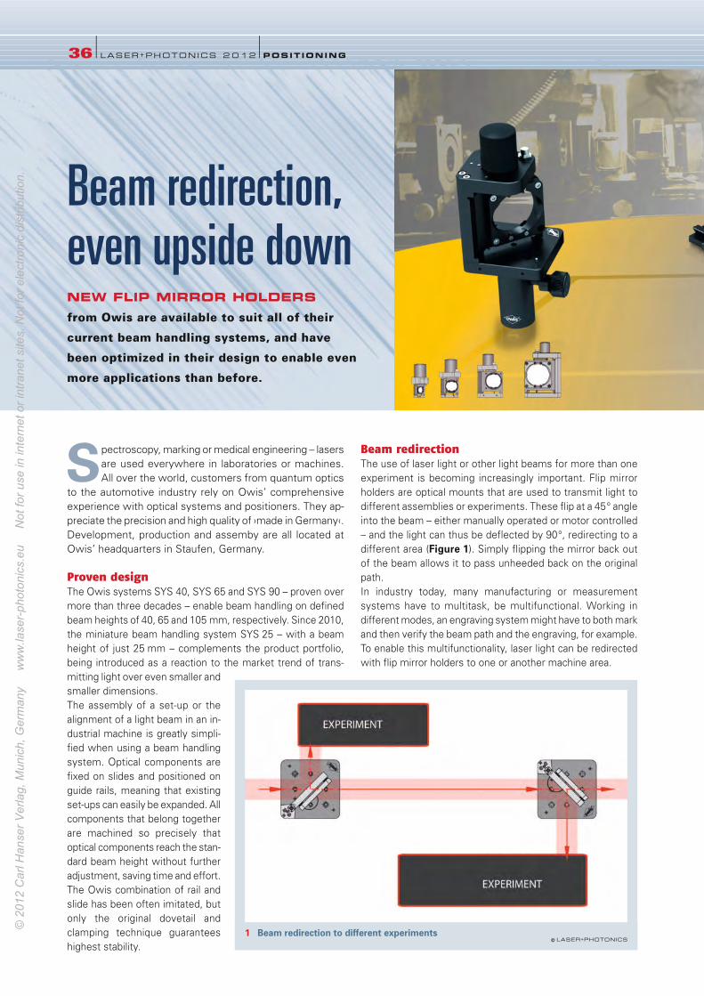
Spectroscopy, marking or medical engineering – lasers
are used everywhere in laboratories or machines.
All over the world, customers from quantum optics
to the automotive industry rely on Owis’ comprehensive
experience with optical systems and positioners. They ap-
preciate the precision and high quality of ›made in Germany‹.
Development, production and assemby are all located at
Owis’ headquarters in Staufen, Germany.
Proven design
The Owis systems SYS 40, SYS 65 and SYS 90 – proven over
more than three decades – enable beam handling on defined
beam heights of 40, 65 and 105 mm, respectively. Since 2010,
the miniature beam handling system SYS 25 – with a beam
height of just 25 mm – complements the product portfolio,
being introduced as a reaction to the market trend of trans-
mitting light over even smaller and
smaller dimensions.
The assembly of a set-up or the
alignment of a light beam in an in-
dustrial machine is greatly simpli-
fied when using a beam handling
system. Optical components are
fixed on slides and positioned on
guide rails, meaning that existing
set-ups can easily be expanded. All
components that belong together
are machined so precisely that
optical components reach the stan-
dard beam height without further
adjustment, saving time and effort.
The Owis combination of rail and
slide has been often imitated, but
only the original dovetail and
clamping technique guarantees
highest stability.
Beam redirection
The use of laser light or other light beams for more than one
experiment is becoming increasingly important. Flip mirror
holders are optical mounts that are used to transmit light to
different assemblies or experiments. These flip at a 45° angle
into the beam – either manually operated or motor controlled
– and the light can thus be deflected by 90°, redirecting to a
different area (Figure 1). Simply flipping the mirror back out
of the beam allows it to pass unheeded back on the original
path.
In industry today, many manufacturing or measurement
systems have to multitask, be multifunctional. Working in
different modes, an engraving system might have to both mark
and then verify the beam path and the engraving, for example.
To enable this multifunctionality, laser light can be redirected
with flip mirror holders to one or another machine area.
36 l LASER+PHOTONICS 2 0 12 lPOSIT IONING
Beam redirection,even upside downNEW FLIP MIRROR HOLDERS from Owis are available to suit all of their
current beam handling systems, and have
been optimized in their design to enable even
more applications than before.
1 Beam redirection to different experiments © LASER+PHOTONICS
36-37_LPX110132_owis_LPex2012 ax 15.12.2011 16:32 Uhr Seite 36
© 2
012
Car
l Han
ser V
erla
g, M
unic
h, G
erm
any
w
ww
.lase
r-ph
oton
ics.
eu
Not
for u
se in
inte
rnet
or i
ntra
net s
ites.
Not
for e
lect
roni
c di
strib
utio
n.
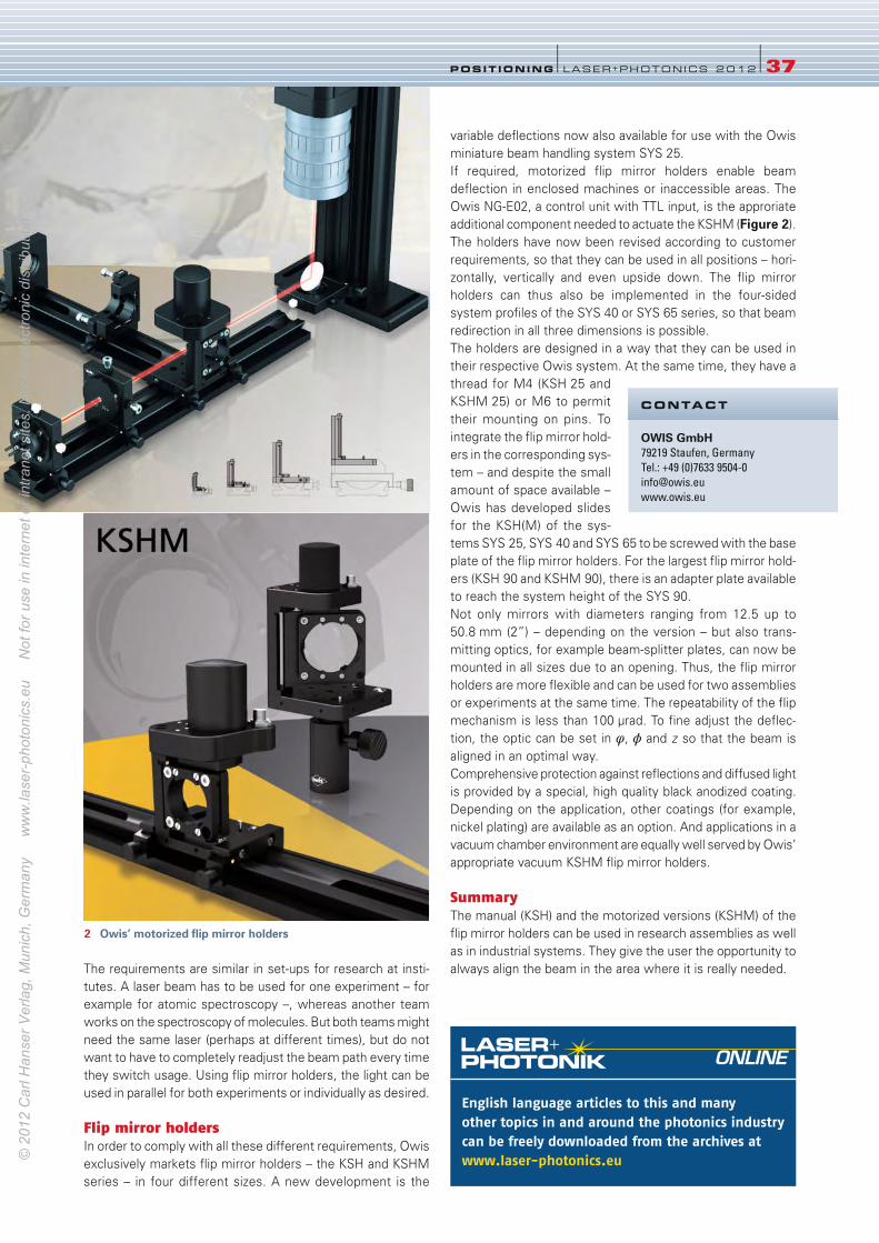
The requirements are similar in set-ups for research at insti-
tutes. A laser beam has to be used for one experiment – for
example for atomic spectroscopy –, whereas another team
works on the spectroscopy of molecules. But both teams might
need the same laser (perhaps at different times), but do not
want to have to completely readjust the beam path every time
they switch usage. Using flip mirror holders, the light can be
used in parallel for both experiments or individually as desired.
Flip mirror holders
In order to comply with all these different requirements, Owis
exclusively markets flip mirror holders – the KSH and KSHM
series – in four different sizes. A new development is the
variable deflections now also available for use with the Owis
miniature beam handling system SYS 25.
If required, motorized flip mirror holders enable beam
deflection in enclosed machines or inaccessible areas. The
Owis NG-E02, a control unit with TTL input, is the approriate
additional component needed to actuate the KSHM (Figure 2).
The holders have now been revised according to customer
requirements, so that they can be used in all positions – hori-
zontally, vertically and even upside down. The flip mirror
holders can thus also be implemented in the four-sided
system profiles of the SYS 40 or SYS 65 series, so that beam
redirection in all three dimensions is possible.
The holders are designed in a way that they can be used in
their respective Owis system. At the same time, they have a
thread for M4 (KSH 25 and
KSHM 25) or M6 to permit
their mounting on pins. To
integrate the flip mirror hold-
ers in the corresponding sys-
tem – and despite the small
amount of space available –
Owis has developed slides
for the KSH(M) of the sys-
tems SYS 25, SYS 40 and SYS 65 to be screwed with the base
plate of the flip mirror holders. For the largest flip mirror hold-
ers (KSH 90 and KSHM 90), there is an adapter plate available
to reach the system height of the SYS 90.
Not only mirrors with diameters ranging from 12.5 up to
50.8 mm (2”) – depending on the version – but also trans-
mitting optics, for example beam-splitter plates, can now be
mounted in all sizes due to an opening. Thus, the flip mirror
holders are more flexible and can be used for two assemblies
or experiments at the same time. The repeatability of the flip
mechanism is less than 100 µrad. To fine adjust the deflec-
tion, the optic can be set in f, o and z so that the beam is
aligned in an optimal way.
Comprehensive protection against reflections and diffused light
is provided by a special, high quality black anodized coating.
Depending on the application, other coatings (for example,
nickel plating) are available as an option. And applications in a
vacuum chamber environment are equally well served by Owis’
appropriate vacuum KSHM flip mirror holders.
Summary
The manual (KSH) and the motorized versions (KSHM) of the
flip mirror holders can be used in research assemblies as well
as in industrial systems. They give the user the opportunity to
always align the beam in the area where it is really needed.
POSIT IONING l LASER+PHOTONICS 2012 l37
OWIS GmbH 79219 Staufen, Germany
Tel.: +49 (0)7633 9504-0
www.owis.eu
CONTACT
2 Owis’ motorized flip mirror holders
English language articles to this and manyother topics in and around the photonics industrycan be freely downloaded from the archives at www.laser-photonics.eu
PHOTONIKLASER+
ONLINE
36-37_LPX110132_owis_LPex2012 ax 15.12.2011 16:32 Uhr Seite 37
© 2
012
Car
l Han
ser V
erla
g, M
unic
h, G
erm
any
w
ww
.lase
r-ph
oton
ics.
eu
Not
for u
se in
inte
rnet
or i
ntra
net s
ites.
Not
for e
lect
roni
c di
strib
utio
n.

MART IN HERMATSCHWEILER
STEFFEN ARNOLD
Following six years of intensive work at the Karlsruhe
Research Center’s Institute for Nanotechnology and
the University of Karlsruhe’s Institute of Applied
Physics, Nanoscribe GmbH was founded at the end of 2007.
In addition to innovative 3D laser lithography equipment,
the dedicated young entrepreneurs offer their customers
services ranging from sample design and production through
to material implementation, for example with silicon. Sup-
port comes from the leading optics concern Carl Zeiss, Zeiss
having shown great interest in the start-up firm’s potential
and emphasizing this by providing both technical and finan-
cial support.
Lithographic detail via laser
The innovative 3D lithography technique that Nanoscribe has
brought to market (Figure 1) permits almost any three-dimen-
sional micro- and nanostructures to be created fully automati-
cally, such as might be required in
tomorrow’s optical technologies. In
principle comparable to the internal
engraving of glass, this new lithog-
raphy method is straightforward to
comprehend and is already suitable
for a wide range of commercially
available photoresists.
Strong focusing of ultrashort laser
pulses precisely exposes photo-
sensitive material located directly
at the focus via a non-linear optical
process. Just like a pen that is
moved in three dimensions, the
laser beam can draw any desired path in the material. Line
widths of several micrometers down to 150 nm can be
achieved, and a total volume of up to 300x300x80 µm3 can
be accessed, depending on the selected microscope lens and
the scanner configuration. As an option, the system can be
adapted for larger, fully automatic structuring volumes or line
widths. A reproducibility of better than 5 nm can be realized.
38 l LASER+PHOTONICS 2 0 12 lPOSIT IONING
A new generation of laser lithography equipment3D STRUCTURING. Laser lithography is already a key technology in many
areas. However, the conventional methods to date are already reaching their limits, both
in research and in industrial applications. A brand new technique now allows very
complex three-dimensional micro- and nanostructures to be produced in photosensitive
materials for the first time.
Physik Instrumente (PI) GmbH & Co. KG76228 Karlsruhe, Germany
Tel. +49 (0)721 4846-0
www.pi.ws
Nanoscribe GmbH 76344 Eggenstein-Leopoldshafen, Germany
Tel. +49 (0)721 608288-40
www.nanoscribe.de
CONTACT
1 Laser lithography systemfor production of three-dimensional micro- andnanostructures
38-41_LPX110110_pi_LPex2012 ax 15.12.2011 16:38 Uhr Seite 38
© 2
012
Car
l Han
ser V
erla
g, M
unic
h, G
erm
any
w
ww
.lase
r-ph
oton
ics.
eu
Not
for u
se in
inte
rnet
or i
ntra
net s
ites.
Not
for e
lect
roni
c di
strib
utio
n.
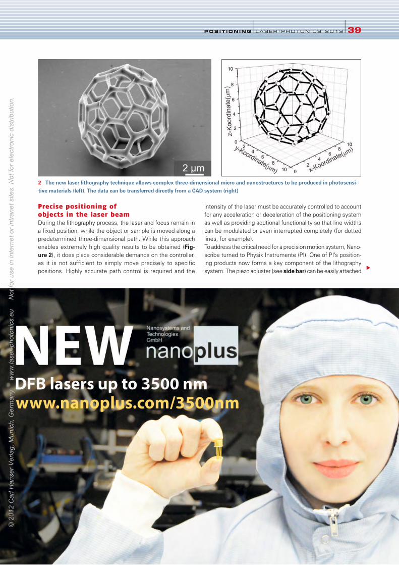
Precise positioning of
objects in the laser beam
During the lithography process, the laser and focus remain in
a fixed position, while the object or sample is moved along a
predetermined three-dimensional path. While this approach
enables extremely high quality results to be obtained (Fig-ure 2), it does place considerable demands on the controller,
as it is not sufficient to simply move precisely to specific
positions. Highly accurate path control is required and the
intensity of the laser must be accurately controlled to account
for any acceleration or deceleration of the positioning system
as well as providing addtional functionality so that line widths
can be modulated or even interrupted completely (for dotted
lines, for example).
To address the critical need for a precision motion system, Nano-
scribe turned to Physik Instrumente (PI). One of PI’s position-
ing products now forms a key component of the lithography
system. The piezo adjuster (see side bar) can be easily attached
POSIT IONING l LASER+PHOTONICS 2012 l39
2 The new laser lithography technique allows complex three-dimensional micro and nanostructures to be produced in photosensi-tive materials (left). The data can be transferred directly from a CAD system (right)
38-41_LPX110110_pi_LPex2012 ax 15.12.2011 16:38 Uhr Seite 39
© 2
012
Car
l Han
ser V
erla
g, M
unic
h, G
erm
any
w
ww
.lase
r-ph
oton
ics.
eu
Not
for u
se in
inte
rnet
or i
ntra
net s
ites.
Not
for e
lect
roni
c di
strib
utio
n.
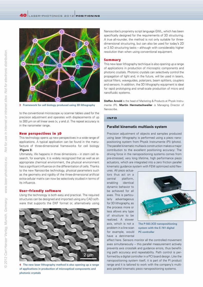
to the conventional microscope xy scanner tables used for the
precision adjustment and operates with displacements of up
to 300 µm on all linear axes (x, y and z). The repeat accuracy is
in the nanometer range.
New perspectives in 3D
This technology opens up new perspectives in a wide range of
applications. A typical application can be found in the manu-
facture of three-dimensional frameworks for cell biology
(Figure 3).
Ultimately, life happens in three dimensions – in stem cell re-
search, for example, it is widely recognized that as well as an
appropriate chemical environment, the physical environment
has a significant influence on the differentiation of cells. Thanks
to the new Nanoscribe technology, physical parameters such
as the geometry and rigidity of the three-dimensional artificial
extra-cellular matrix can now be selectively studied in terms of
its influence.
User-friendly software
Using the technology is both easy and practical. The required
structures can be designed and imported using any CAD soft-
ware that supports the DXF format or, alternatively using
Nanoscribe’s proprietry script language GWL, which has been
specifically designed for the requirements of 3D structuring.
A true all-rounder, the method is not only suitable for three-
dimensional structuring, but can also be used for today’s 2D
or 2.5D structuring tasks – although with considerably higher
resolution than when using conventional equipment.
Summary
This new laser lithography technique is also opening up a range
of applications in production of microoptic components and
photonic crystals. Photonic crystals can selectively control the
propagation of light and, in the future, will be used in lasers,
optical filters, waveguides, polarizers, beam splitters, couplers
and sensors. In addition, the 3D lithography equipment is ideal
for rapid prototyping and small-scale production of micro and
nanofluidic systems.
Steffen Arnold is the head of Marketing & Products at Physik Instru-
mente (PI). Martin Hermatschweiler is Managing Director of
Nanoscribe.
40 l LASER+PHOTONICS 2 0 12 lPOSIT IONING
4 The new laser lithography method is also opening up a rangeof applications in production of microoptical components andphotonic crystals
3 Framework for cell biology produced using 3D lithography
Parallel kinematic multiaxis system
Precision adjustment of objects and samples produced
using laser lithography is performed using a piezo nano-
positioning system from Physik Instrumente (PI) (photo).
The parallel kinematic multiaxis construction makes a major
contribution to the excellent positioning accuracy: The
driving force in the nanopositioning systems comes from
pre-stressed, very long lifetime, high performance piezo
actuators, which are integrated into a zero friction parallel
kinematic guidance system with FEM optimized solid flex-
ures. All piezo actua-
tors thus act on a
central platform,
enabling identical
dynamic behavior to
be achieved for all
axes. This is particu-
larly advantageous
for 3D lithography, as
the process more or
less allows any type
of structure to be
realized. A slower
axis, which is not a
problem in a line scan
for example, would
have a detrimental
effect here. Sensors monitor all the controlled movement
axes simultaneously – this parallel measurement actively
prevents axis crosstalk and guidance errors, thus benefit-
ing path accuracy and repeatability. Path control is per-
formed by a digital controller in a PCI board design. Like the
nanopositioning system itself, it is part of the PI product
range and it is tailored to work with the company’s multi-
axis parallel kinematic piezo nanopositioning systems.
INFO
The P-563.3CD nanopositioningsystem with the E-761 digital PC controller
38-41_LPX110110_pi_LPex2012 ax 15.12.2011 16:39 Uhr Seite 40
© 2
012
Car
l Han
ser V
erla
g, M
unic
h, G
erm
any
w
ww
.lase
r-ph
oton
ics.
eu
Not
for u
se in
inte
rnet
or i
ntra
net s
ites.
Not
for e
lect
roni
c di
strib
utio
n.
Carl Hanser Verlag GmbH & Co. KG · P.O. Box 86 04 20 · 81631 Munich/Germany · Tel.: +49 89 99830-0 · Fax: +49 89 984809
T E C H N I C A L M AG A Z I N E S | T E C H N I C A L BO O K S | O N L I N E S E R V I C E S | S E M I N A R S & CO N F E R E NC E S
Seminars & Conferences
Technical Books
Technical Magazines
Online Services
Profound Knowledge in a Flexible Multi-Media System:
Since 1928 Hanser Publishers have established themselves as
competent providers of information. Hanser Publishers do not
only offer you 19 technical magazines and almost 3.400 technical
and textbooks in the fields of computer, engineering, and
management & business but also specific portals and practical
seminars for a successful career. Read more at www.hanser.de
38-41_LPX110110_pi_LPex2012 ax 15.12.2011 16:39 Uhr Seite 41
© 2
012
Car
l Han
ser V
erla
g, M
unic
h, G
erm
any
w
ww
.lase
r-ph
oton
ics.
eu
Not
for u
se in
inte
rnet
or i
ntra
net s
ites.
Not
for e
lect
roni
c di
strib
utio
n.
The CompanyLeistungselektronik JENA GmbH (LEJ) was
formed in 1991 as a spin-off of the research
center of Carl Zeiss Jena GmbH. More than 25
years of continuous research and product
development in the field of ballasts for gas dis-
charge lamps and complete light sources are
the basis of LEJ as a technology company.
LEJ supplies a wide range of standard pro-
ducts, plus custom modifications for sophisti-
cated industrial application and use in research
and development.
The products– High-stability ballasts, lamp housings, igni-
tion modules and compact light sources,
glass fiber link, if needed, based on mercu-
ry, xenon and mixed gas lamps in the output
range of 50 W to 2000 W.
– Electronic ballasts and luminaires for high-
power light sources using metal halide, sodi-
um vapor or other comparable of 150 W to
2500 W output.
– Xenon flashers for industrial use in different
versions, coupling in optical fibers, flash
energy and frequency adjustable, up to 10
Ws or 100 Hz.
– Lighting modules based on high-power LEDs
in different configurations
– Electronic ballasts, processor-controlled,
programmable, for UV high power radiation
sources for DC or AC, output range from 500
W to 2000 W
– Custom modifications of all standard pro-
ducts, tungsten halogen and deuterium lamp
supplies
ApplicationsThe products find application in:
precision mechanical/optical industries, indus-
trial image processing, analytical products, pro-
jection, environmental simulation/solar simu-
lation, UV disinfection
Leistungselektronik JENA GmbHMORE THAN LIGHT
Leistungselektronik JENA GmbH
Stockholmer Str. 5
07747 Jena
Germany
Phone +49 (0)3641 35300
Fax +49 (0)3641 3530-70
www.lej.de
42 lCOMPANY PROF ILE
COMPANY PROF ILE
mechOnics ag– Competence in micropositioning –
mechOnics ag, a German company founded in
2003, is specialized in development, produc-
tion and sales of systems for micro- and
nanopositioning applications.
These systems are driven by a new developed,
innovative piezo inertial drive, which combines
high resolution in the nm-range with large trav-
els up to 50 mm. Together with piezo con-
trollers with very low power consumption this
permits main voltage free applications in labo-
ratories and out of doors.
In telecommunication, semiconductor indus-
try, laser- and bio-technology, sensors and
space industry multiple customers profit of the
high competence of mechOnics.
Range of standard productsLinear stages up to 50 mm travel
Ultra compact xyz-stages (travel ≤ 10 mm)
Monomode coupler (travel ≤ 2 mm)
Ultra low temperature stages (≤ 300 mK)
Ultra high vacuum stages (≤ 10-10 Torr)
Mirror mounts for transm. optics (tilt ± 3 deg.)
Linear measuring systems (resolution < 50 nm)
Handheld battery driven controller
USB-controller (open or closed loop)
Customized productsPositioners for ultra low temperature
applications
Low temperature microscopes
Slits for electronic microscopy
Filter slider for space applications
Positioners for UHV applications
mechOnics agCompetence in MicropositioningUnnützstr. 2/B
81825 München
Germany
Phone +49 (0)89 42024207
Fax +49 (0)89 42024206
www.mechonics.de
_FP_LPex2012 14.12.2011 15:52 Uhr Seite 42
© 2
012
Car
l Han
ser V
erla
g, M
unic
h, G
erm
any
w
ww
.lase
r-ph
oton
ics.
eu
Not
for u
se in
inte
rnet
or i
ntra
net s
ites.
Not
for e
lect
roni
c di
strib
utio
n.
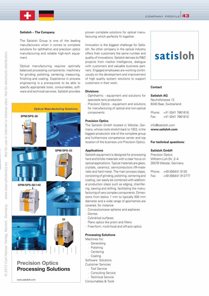
COMPANY PROF ILE l43
Contact
Satisloh AGNeuhofstrasse 12
6340 Baar, Switzerland
Phone: +41 (0)41 7661616
Fax: +41 (0)41 7661610
www.satisloh.com
For technical questions:
Satisloh GmbHPrecision Optics
Wilhelm-Loh-Str. 2–4
35578 Wetzlar, Germany
Phone: +49 (0)6441 9120
Fax: +49 (0)6441 912777
Satisloh – The Company
The Satisloh Group is one of the leading
manufacturers when it comes to complete
solutions for ophthalmic and precision optics
manufacturing and reliable high-tech equip-
ment.
Optical manufacturing requires optimally
balanced processing components: machinery
for grinding, polishing, centering, measuring,
finishing and coating. Experience in process
engineering is a prerequisite to be able to
specify appropriate tools, consumables, soft-
ware and technical services. Satisloh provides
proven complete solutions for optical manu-
facturing which perfectly fit together.
Innovation is the biggest challenge for Satis-
loh. No other company in the optical industry
offers their customers the same number and
quality of innovations. Satisloh derives its R&D
projects from market intelligence, dialogue
with customers and valuable business part-
ners. Engaged employees are working contin-
uously on the development and improvement
of high quality system solutions to support
customers in their work.
Divisions:· Ophthalmic - equipment and solutions for
spectacle lens production
· Precision Optics - equipment and solutions
for manufacturing of optical and non-optical
components
Precision OpticsThe Satisloh GmbH located in Wetzlar, Ger-
many, whose roots stretch back to 1922, is the
biggest production site of the complete group
and furthermore competence center and top
location of the business unit Precision Optics.
ApplicationsSatisloh equipment is designed for processing
hard and brittle materials with a clear focus on
optical applications. Typical materials are glass,
crystals, ceramics, semiconductors (IR-mate-
rials) and hard metal. The main process steps,
consisting of grinding, polishing, centering and
coating, can easily be combined with addition-
al production steps such as edging, chamfer-
ing, sawing and drilling, facilitating the manu-
facturing of very complex components. Dimen-
sions from below 1 mm to typically 500 mm
diameter and a wide range of geometries are
covered, for instance:
· Convex/concave spheres and aspheres
· Domes
· Cylindrical surfaces
· Plano optics like prism and filters
· Free-form, multi-focal and off-axis optics
Processing SolutionsMachines for:
· Generating
· Polishing
· Centering
· Coating
Software Solutions
Customer Services
· Tool Service
· Consulting Service
· Technical Service
Consumables & Tools
_FP_LPex2012 14.12.2011 15:52 Uhr Seite 43
© 2
012
Car
l Han
ser V
erla
g, M
unic
h, G
erm
any
w
ww
.lase
r-ph
oton
ics.
eu
Not
for u
se in
inte
rnet
or i
ntra
net s
ites.
Not
for e
lect
roni
c di
strib
utio
n.

44 lCOMPANY PROF ILE
COMPANY PROF ILE
Instrument Systems GmbH Neumarkter Str. 83
81673 Munich
Germany
Phone +49 (0)89 454943-0
Fax +49 (0)89 454943-11
www.instrumentsystems.com
Solutions for light measurement Instrument Systems, founded in 1986, is a
leading manufacturer for light measurement
solutions. The portfolio includes array and scan-
ning spectroradiometers, and imaging
photometers and colorimeters. Headquarters
are located in Munich and the global customer
base is supported by a worldwide network of
representatives.
Core competenciesLED measurement Instrument Systems continues to set the
benchmark in LED metrology. Whether test-
ing single LEDs (standard or high-power), LED
modules, or OLEDs - the company engineers
turnkey solutions ranging from high-speed pro-
duction testing to high-
performance spectro-
radiometers (e.g. CAS
140 CT series) for R&D
and QC. The instru-
ments provide accu-
rate and reliable re-
sults as per CIE recom-
mendations for all relevant parameters like lu-
minous intensity, luminous flux, chromaticity
coordinates and color rendering index.
Display measurement Instrument Systems offers a wide range of re-
fined and proven systems for testing displays.
The LumiCam 1300 and LumiCam 4000 imag-
ing photometers and colorimeters with GigE
interface determine luminance, chromaticity,
color temperature and dominant wavelength
in a fast and accurate way. The high-resolution
LumiCam 4000 captures and evaluates around
11 million pixels simultaneously in a single
measurement.
Spectroradiometry and photometry Scanning spectrometers based on single or
double monochromators are used for precise
determination of radiant pow-
er, radiant intensity and irradi-
ance. The SPECTRO 320 series
covers a spectral range from
190 to 5000 nm and meets the
highest requirements for wave-
length accuracy, signal dynam-
ic range and low stray light.
STEMMER IMAGING GmbHGutenbergstraße 9 – 13
82178 Puchheim
Phone +49 (0)89 80902-0
Fax +49 (0)89 80902-116
www.stemmer-imaging.com
STEMMER IMAGING: IMAGINGIS OUR PASSION
STEMMER IMAGING is Europe's largest imag-
ing technology provider with offices in Ger-
many, United Kingdom, France and Switzerland
(Pfäffikon near Zurich).
At STEMMER IMAGING, customers find the
complete technical range of products from the
world's leading manufacturers. Together, these
technologies provide cutting-edge machine vi-
sion solutions across all application areas. With
several thousand components and solutions
available, we are able to deliver the majority of
orders directly from stock.
STEMMER IMAGING are the developers of the
world's leading image processing development
environment, Common Vision Blox (CVB, see
www.commonvisionblox.com), and also manu-
facture application-specific products to enable
complex solutions to be realised easily.
STEMMER IMAGING does not install end user
solutions - instead, using our close partnerships
with a large number of experienced system
integrators, we can provide expert technical
know-how for the planning, integration and
realisation of complete solutions.
Our broad range of components and solutions,
in combination with over 30 years of imaging
experience and more than 150 employees,
STEMMER IMAGING is your reliable and com-
petent imaging partner.
STEMMER IMAGING - IMAGING IS OURPASSION!
_FP_LPex2012 14.12.2011 15:52 Uhr Seite 44
© 2
012
Car
l Han
ser V
erla
g, M
unic
h, G
erm
any
w
ww
.lase
r-ph
oton
ics.
eu
Not
for u
se in
inte
rnet
or i
ntra
net s
ites.
Not
for e
lect
roni
c di
strib
utio
n.
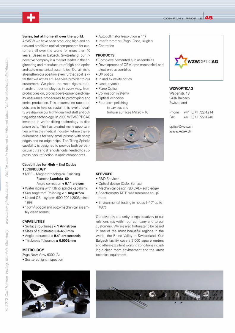
COMPANY PROF ILE l45
Swiss, but at home all over the world.At WZW we have been producing high-end op-
tics and precision optical components for cus-
tomers all over the world for more than 40
years. Based in Balgach, Switzerland, our in-
novative company is a market leader in the en-
gineering and manufacture of high-end optics
and opto-mechanical assemblies. Our aim is to
strengthen our position even further, so it is vi-
tal that we act as a full-service provider to our
customers. We place the most rigorous de-
mands on our employees in every way, from
product design, product development and qual-
ity assurance procedures to prototyping and
series production. This ensures first-rate prod-
ucts, and to help us sustain this level of quali-
ty we draw on our highly qualified staff and cut-
ting-edge technology. In 2009 WZWOPTICAG
invested in wafer dicing technology to dice
prism bars. This has created many opportuni-
ties within the medical industry, where the re-
quirement is for very small prisms with sharp
edges and no edge chips. The Tilting Spindle
capability is designed to provide both perpen-
dicular cuts and 8° angular cuts needed to sup-
press back-reflection in optic components.
Capabilities for High – End OpticsTECHNOLOGY• MRF – Magnetorheological Finishing
Flatness Lambda 60Angle correction < 0.1” arc sec
• Wafer dicing with tilting spindle capability
• Sub Angstrom Polishing < 1 Angström• Linked QS – system (ISO 9001:2008) since
1998
• 150m2 optical and opto-mechanical assem-
bly clean rooms
CAPABILITIES• Surface roughness < 1 Angström• Sizes of substrates 0.3–450 mm• Angle tolerances ± 0.4” arc seconds• Thickness Tolerance ± 0.0002mm
METROLOGYZygo New View 6300 (Å)
• Scattered light inspection
• Autocollimator (resolution ± 1”)
• Interferometer ( Zygo, Fisba, Kugler)
• Centration
PRODUCTS• Complexe cemented sub assemblies
• Development of OEM opto-mechanical and
electronic assemblies
• UV optics
• In and ex cavity optics
• Laser crystals
• Plano Optics
• Collimation systems
• Optical windows
• Free form polishing
in cavities and
turbular surfaces Mil 20 – 10
SERVICES• R&D Services
• Optical design (Oslo, Zemax)
• Mechanical design (3D CAD- solid edge)
• Spectrometry MTF measurement equip-
ment
• Environmental testing in house (–40º up to
180º)
Our diversity and unity brings creativity to our
relationships within our company and to our
customers. We are also fortunate to be based
in one of the most beautiful regions in the
world, the Rhine Valley in Switzerland. Our
Balgach facility covers 3,000 square meters
and offers excellent working conditions includ-
ing a clean room environment and the latest
technical equipment.
WZWOPTICAGWegenstr. 18
9436 Balgach
Switzerland
Phone +41 (0)71 722-1214
Fax +41 (0)71 722-1240
www.wzw.ch
_FP_LPex2012 14.12.2011 15:53 Uhr Seite 45
© 2
012
Car
l Han
ser V
erla
g, M
unic
h, G
erm
any
w
ww
.lase
r-ph
oton
ics.
eu
Not
for u
se in
inte
rnet
or i
ntra
net s
ites.
Not
for e
lect
roni
c di
strib
utio
n.
Cost-effective racersLine scan cameras. Basler has just intro-
duced the first models of their new com-
pact and cost-effective line scan camera
family ›racer‹. The cameras are available
with either a Gigabit Ethernet or a Cam-
eraLink interface. They use the latest line
scan sensors based on highly sensitive
CMOS technology and reach line rates of
up to 48 kHz via Gigabit Ethernet and up
to 80 kHz with the CameraLink interface.
The fist models offer 2k and 4k resolu-
tions, cameras with 8k and 12k will follow
in the course of 2012. This new series is
designed to cover the whole spectrum of
standard line scan cameras, making it
easier for users from many different
markets and application areas to choose
suitable cameras for their needs. The
CameraLink models are equipped with
Power over Camera Link (PoCL) support
so that data and power are transported
over the same cable, reducing both over-
all costs for accessories and system com-
plexity. The compact cameras with an in-
dustrial housing (w x h, 56 x 62 mm2) are
ideally suited for multi-camera designs,
especially in applications where many line
scan cameras are installed side-by-side.
www.baslerweb.com
Improved fluorescence imagingsCMOS camera. Hamamatsu Photonics
Germany introduces their new ›Orca-
Flash4.0‹ 4 MP sCMOS camera, engi-
neered around a new second-generation
sCMOS detector. The camera promises
high sensitivity, high resolution and a fast
readout, with a significantly improved
signal-to-noise for low-level, fast fluores-
cence imaging. This enables the camera
to cover a wide range of imaging needs,
including super resolution microscopy,
TIRF microscopy, live cell GFP, high-speed
calcium ion imaging, FRET, real-time
confocal microscopy and many more. The
Orca-Flash4.0 has quantum efficiency
values of over 70 percent at 600 nm and
50 percent at 750 nm and has only 1.3
electrons of read noise (at 100 full-reso-
lution frames per second) with continu-
ous high speed acquisition at full resolu-
tion. This combination of high quantum
efficiency and low noise, in the absence
of EM-CCD multiplicative noise, makes
the camera ideally suited for demanding
microscopy applications.
www.hamamatsu.de
46 l LASER+PHOTONICS 2 0 12 lPRODUCT MARKETPLACE
Landstrasse 16 I Postfach I FL-9496 BalzersTelefon +423/ 388 11 50-53 I Fax +423/ 388 11 55E-Mail [email protected] I www.filtrop.com
FILTROP AG –Development, manufacturing and supply of :
� OpticsOptical F i l ters I Optical Coatings I OpticalComponents I Optical Raw Materials
� Wet-chemical CoatingsSol-Gel-Nanocomposite Coatings I FluorpolymerCoatings I Decorative Coatings
� Small Tubes and CapillariesFor use in Autosampling, Automatic Dispensing,In-Vitro Measurements, Cl inical Chemistry,Chromatography, Dental Industry, Human Medecine Gr
afik
SiR
up
FILTROP AG –Your Supply-Chain!
46-47_produkte_LPex2012_x 15.12.2011 16:42 Uhr Seite 46
© 2
012
Car
l Han
ser V
erla
g, M
unic
h, G
erm
any
w
ww
.lase
r-ph
oton
ics.
eu
Not
for u
se in
inte
rnet
or i
ntra
net s
ites.
Not
for e
lect
roni
c di
strib
utio
n.

PRODUCT MARKETPLACE l LASER+PHOTONICS 2012 l47
Fully customizableUSB camera platform. Framos presents
the new ›Visiosens VFU‹ camera series,
a highly flexible and customizable imag-
ing platform with more than 140 camera
variants per image sensor and a uniform
software interface for all models. The
series is available with USB 2.0 as well
as the latest USB 3.0 interface enabling
up to 5 Gbit/s. The platform consists of a
growing number of image sensors
(CMOS and CCD sensors with resolu-
tions from 0.3 to 10 MP), a variety of
output interfaces, complementary as-
sembly concepts, mounts (C-, CS- or
M12-mount), filters, and, optionally, an
LED lighting ring integrated in the hous-
ing and connected to the 8-pin I/O port.
For all variants, the user and system in-
terface is built on a unified, future-proof,
cross-platform software development kit
based on the latest ›.NET‹ technology.
The robust camera housing was specifi-
cally designed for industrial systems as
well as for microscopy. It offers multiple
mounting options on each side and the
front face which are all symmetrical to
the optical axis of the sensor.
www.framos.de
High flexibilityBoard level camera series. Baumer has
designed their new MXG board level
camera series specifically to meet the
growing demand for miniaturization and
higher flexibility. The separate sensor
board measures only 28 x 28 mm2 and is
connected to the system circuit board via
flexprint, allowing the cameras to be in-
dividually integrated even into small,
cramped spaces. The series comprises
four monochrome and four color cameras
with resolutions ranging from VGA up to
4 MP, featuring CCD sensors, as well as
a 4 MP CMOS sensor from Cmosis. The
first model available offers VGA resolu-
tion and a 140 fps transfer capability.
While Trigger Delay simplifies synchro-
nization between the application and the
camera, the sequencer makes it much
easier to capture image series with
changing acquisition parameters. Both
Packet Delay and Transmission Delay
modes are available to support reliable
data transfer in multi-camera operation.
Storable user sets and the GigE standard
interface with Power over Ethernet help
simplify camera integration.
www.baumer.com/cameras
Illumination... for machine vision. The ›intraLED 3‹
LED light source from Volpi promises a
service life of 50,000 h and a light inten-
sity of more than 500 lm (measured on a
1m light guide with an active diameter of
13.5 mm). As the follow-up model to the
›intraLED 2020+‹, it has been specially
designed for machine vision applications,
providing a 30 percent increase in power
and a typical color temperature of 6000 K.
It is actuated either manually, using the
integrated RS-232 interface (USB option-
al) or using the Multiport with digital and
analog input. Its power consumption is
24 VDC with a maximum of 55 W. The
compact enclosure makes it easy to use
in small spaces, while the threaded bars
(M4) on four sides ensure trouble-free
system integration. The intraLED 3 is avail-
able in two versions, making it compati-
ble with light guides from both Volpi and
Schott-Fostec. For applications that de-
mand a higher light intensity, Volpi offers
the IntraLED 5, based on the same design
platform as the intraLED 3 and delivering
more than 700 lm. www.volpi.ch
46-47_produkte_LPex2012_x 15.12.2011 16:42 Uhr Seite 47
© 2
012
Car
l Han
ser V
erla
g, M
unic
h, G
erm
any
w
ww
.lase
r-ph
oton
ics.
eu
Not
for u
se in
inte
rnet
or i
ntra
net s
ites.
Not
for e
lect
roni
c di
strib
utio
n.
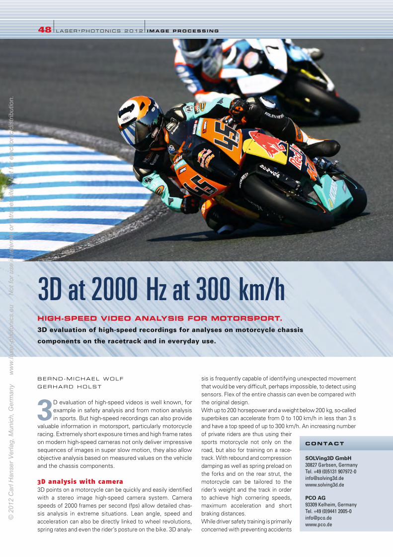
BERND-MICHAEL WOLF
GERHARD HOLST
3D evaluation of high-speed videos is well known, for
example in safety analysis and from motion analysis
in sports. But high-speed recordings can also provide
valuable information in motorsport, particularly motorcycle
racing. Extremely short exposure times and high frame rates
on modern high-speed cameras not only deliver impressive
sequences of images in super slow motion, they also allow
objective analysis based on measured values on the vehicle
and the chassis components.
3D analysis with camera
3D points on a motorcycle can be quickly and easily identified
with a stereo image high-speed camera system. Camera
speeds of 2000 frames per second (fps) allow detailed chas-
sis analysis in extreme situations. Lean angle, speed and
acceleration can also be directly linked to wheel revolutions,
spring rates and even the rider’s posture on the bike. 3D analy-
sis is frequently capable of identifying unexpected movement
that would be very difficult, perhaps impossible, to detect using
sensors. Flex of the entire chassis can even be compared with
the original design.
With up to 200 horsepower and a weight below 200 kg, so-called
superbikes can accelerate from 0 to 100 km/h in less than 3 s
and have a top speed of up to 300 km/h. An increasing number
of private riders are thus using their
sports motorcycle not only on the
road, but also for training on a race-
track. With rebound and compression
damping as well as spring preload on
the forks and on the rear strut, the
motorcycle can be tailored to the
rider’s weight and the track in order
to achieve high cornering speeds,
maximum acceleration and short
braking distances.
While driver safety training is primarily
concerned with preventing accidents
48 l LASER+PHOTONICS 2 0 12 l IMAGE PROCESSING
3D at 2000 Hz at 300 km/hHIGH-SPEED VIDEO ANALYSIS FOR MOTORSPORT. 3D evaluation of high-speed recordings for analyses on motorcycle chassis
components on the racetrack and in everyday use.
SOLVing3D GmbH 30827 Garbsen, Germany
Tel. +49 (0)5131 907972-0
www.solving3d.de
PCO AG 93309 Kelheim, Germany
Tel. +49 (0)9441 2005-0
www.pco.de
CONTACT
48-51_LPX110128_pco_LPex2012 ax 15.12.2011 16:46 Uhr Seite 48
© 2
012
Car
l Han
ser V
erla
g, M
unic
h, G
erm
any
w
ww
.lase
r-ph
oton
ics.
eu
Not
for u
se in
inte
rnet
or i
ntra
net s
ites.
Not
for e
lect
roni
c di
strib
utio
n.

on the road by safe emergency braking and hazard
avoidance, when it comes to riding on a racetrack,
a fast lap is the top priority. Both areas benefit from
the rider’s ability to optimally slow down the bike.
Measurement strategy
A small number of measurement markers attached
to the bike at clearly visible points allow a complete
analysis of the interaction between the individual
chassis components.
On a racetrack, one typically accelerates on the
straights and brakes as late and as hard as possi-
ble just before entering a corner. Figure 1 shows
the braking at the end of the back straights at the
Oschersleben Motopark (Germany), from speeds
of well over 200 km/h down to around 120 km/h.
The recording enables the exact braking point and the maxi-
mum deceleration to be determined as well as the spring
travel on the forks and the position of the rear of the bike to be
measured. The remaining spring travel on the front wheel can
also be measured and must remain in control without bottom-
ing out. The high resolution of a high-speed camera together
with high sensitivity and low noise enables the initial response
of the motorbike, which is critical for a short braking distance.
The build-up of braking rate can also be measured.
Maximum deceleration allows late braking points and there-
fore longer acceleration periods. For example, imagine two
riders, A and B, both of whom are at a speed of 200 km/h at
the braking point and which needs to be reduced to 100 km/h
at the end of braking. Rider A requires 0.3 s for maximum
braking to be achieved, rider B just 0.1 s. This means that
rider B can start braking 10 m later, thus gaining a crucial lead
at the entrance to the corner.
In the acceleration phase at the exit from the corner, as can be
seen in Figure 2, the performance of the rear end is crucial.
Here, a 3D analysis allows the lean and acceleration to be
determined, in conjunction with an analysis of the suspension
and damping on the rear of the bike.
IMAGE PROCESSING l LASER+PHOTONICS 2012 l49
CompoTRON
Germany +49 89 538866-0
www.compotron.com
11010015 W
WW.2
PU
NKT.
DE
Innovative SolutionsSFP+ SR, LR 10km, LR 20km, ER 40km & CWDM
XFP SR/LR/ER/ZR/ER & ZR DWDM/120km
Customised Labelling, EEPROM, Packaging etc.
Robust ESD and Thermal Solutions
Crystals, Oscillators, TCXO, VCTCXO & VCXO
MSA Transceiver ProductsSFP LC Duplex & Bi-Di, DDM, opt. F-3000 Connector
SFF 2x5 LC Duplex & SC Bi-Di
1x9 SC (Shielding Optional), ST, FC & SC Bi-Di
–40°C to 85°C/120km GbE & 200km FE
XFP, SFP Cages and Connectors
Specialty PhotonicsFibers, Cables and Assemblies
Specialty Single Mode, HCS, PYROCOAT®
Metalized, Carbon Coated, Tight Bend Radius
Crimp and Cleave Fiber Termination Kits
ISO 9001 and ISO 13485 certified
Fiber Optics for Industrial, Medical and Communications Applications
1 Braking from a high speed
48-51_LPX110128_pco_LPex2012 ax 15.12.2011 16:46 Uhr Seite 49
© 2
012
Car
l Han
ser V
erla
g, M
unic
h, G
erm
any
w
ww
.lase
r-ph
oton
ics.
eu
Not
for u
se in
inte
rnet
or i
ntra
net s
ites.
Not
for e
lect
roni
c di
strib
utio
n.

Applications away from the racetrack
The same technology can also help participants in driver safe-
ty training to learn about emergency braking. Unlike in a car,
the braking distance on a motorbike depends hugely on the
individual abilities of the rider. Training and practice on a closed
track are essential for achieving maximum deceleration when
braking. The reason for this is that the front wheel in particular
should not lock, as this almost inevitably leads to a crash. How-
ever, fear of crashing due to a locked front wheel often hinders
the rider from rapidly reaching full braking potential, which is
essential in achieving the shortest possible braking distance.
Table A illustrates the relationship between three different times
a rider requires to reach maximum braking and the resulting
braking distances for full braking, both from 50 km/h and from
100 km/h (a linearly increasing deceleration of 0 to 10 m/s2 is
assumed). From 50 km/h the braking distance is extended by
up to 5 m, from 100 km/h by up to 10 m. Even more revealing
are the speeds Ve with which the ‘slower’ riders are still
moving after 10.7 or 40.8 m (at which points the ‘fast’ reacting
rider is already at a standstill).
3D analysis with a single camera
A 3D video analysis system such as the ›SOLVing3D.titan‹
system is made up of a low-noise, high-speed camera system
(the ›pco.dimax‹ in this case) and a stereo mirror attachment
(Figure 3). The high resolution sensor on the pco.dimax has
2016x2016 pixels and the stereo mirror attachment used in the
SOLVing3D.titan system has a fixed stereo basis of 300 mm
and slightly convergent acquisition axes.
The two stereo images are normally mapped to the central area
of the sensor (2016x1008) and thus resulting in two image
sequences during the recording – each with 1008x1008 pixels
and slightly different angles of view. The system provides an
exceptional image quality and resolution of the 3D stereo film,
in color and at a frame rate of 2128 fps.
The system is calibrated in the same way as a normal stereo
camera system. After appropriate conversion, two time-
synchronous image sequences from the virtual stereo camera
are obtained, which can be evaluated in 3D. This kind of sys-
tem is very compact, robust and comparatively easy to use. A
disadvantage of the titan system compared to a stereo meas-
urement system with two cameras is the reduced flexibility in
the choice of location due to the fixed geometry of the mirror
attachment. The advantages are the very robust operation and
the elimination of synchronization errors and differently exposed
stereo sequences.
When analyzing the recordings, the accompanying software
provides comprehensive functions for calculating and display-
50 l LASER+PHOTONICS 2 0 12 l IMAGE PROCESSING
Time [s] Vs [km/h] Braking distance [m] Ve [km/h]
0.3 50 10.7 0
0.5 50 12.3 21
1.0 50 15.4 37
0.3 100 40.8 0
0.5 100 44.0 31
1.0 100 50.6 52
A Braking distances (fullbraking) for different rider
reaction times, specified for50 and 100 km/h. Also
shown are the final speedsof riders with slower reac-
tions, measured at the endof the braking distance ofthe rider with the fastest
reaction time
3 The ›SOLVing3D.titan‹ 3D video analysis system
2 Accelerating outof a corner
48-51_LPX110128_pco_LPex2012 ax 15.12.2011 16:46 Uhr Seite 50
© 2
012
Car
l Han
ser V
erla
g, M
unic
h, G
erm
any
w
ww
.lase
r-ph
oton
ics.
eu
Not
for u
se in
inte
rnet
or i
ntra
net s
ites.
Not
for e
lect
roni
c di
strib
utio
n.

ing the measured results (Figure 4). This enables analysis of
parameters such as position, speed, acceleration, orientation
and trajectory progressions to be determined quickly. The
software supports evaluation with menu-based evaluation
processes.
The software can also be used to geometrically correct the
image sequences so that they can be viewed stereoscopical-
ly. The resulting 3D impression often makes it easier to inter-
pret the measured values. For close-up applications the
SOLVing3D.titan system achieves
accuracies of 0.3 mm.
A further advantage of the measure-
ment system over the individual meas-
urement sensors mentioned above
(which would have to be attached to
the motorbike along with the corre-
sponding data capture equipment), is
that only low-cost point markers have
to be attached to the bike or to the
rider. Only one set of measurement
equipment is required and can thus be
used directly for multiple bikes. This
enables comparative analyses be-
tween different riders and bikes to be
carried out. This makes the system
ideal for analysis within small groups
– including driver safety training.
Summary
Using high-speed 3D video analysis in driver safety and race-
track training provides valuable information to improve motor-
bike and rider behavior. This kind of measurement system can
also be used for other applications such as crash testng, motion
analysis in various branches of sport and much more.
Dr. Gerhard Holst is the head of the science and research department
at PCO. Dr. Bernd-Michael Wolf is Executive Director at SOLVing3D.
IMAGE PROCESSING l LASER+PHOTONICS 2012 l51
4 Software interface for the ›SOLVing3D.titan‹ system
Enabling InnovativeOptical Solutions
Optics Balzers has been the preferred
partner for innovative optical solutions for
more than 65 years. As a global leader,
Optics Balzers focuses on high-tech markets such as
Sensors & Imaging, Biophotonics, Space & Defence,
Lighting & Projection, and Industrial Applications.
The company possesses comprehensive know-how
in optical thin-film coatings and components, glass
processing, patterning and sealing technologies.
Optics Balzers AGBalzers/Liechtenstein
Optics Balzers Jena GmbHJena/Germany
www.opticsbalzers.com
Prismastrasse 5CH-9444 DiepoldsauSwitzerlandFon +41 71 737 74 00Fax +41 71 737 74 10www.zuendoptics.com
Autoclavable
compact prisms
and roof prisms
in sizes between
0.3 and 5.0 mm
in all desired
divergences.
zünd precision optics
Perfection in detailEndoscopyEquipped for the future
48-51_LPX110128_pco_LPex2012 ax 15.12.2011 16:46 Uhr Seite 51
© 2
012
Car
l Han
ser V
erla
g, M
unic
h, G
erm
any
w
ww
.lase
r-ph
oton
ics.
eu
Not
for u
se in
inte
rnet
or i
ntra
net s
ites.
Not
for e
lect
roni
c di
strib
utio
n.

GREGORY FL INN
Jenoptik was restructured four years ago, what were thereasons for this change? Dirk Rothweiler: It was certainly the right step to take! The new
logical grouping of Jenoptik, with its portfolios of products and
technologies, better aligned our activities with customers and
markets. The restructuring was actually not all that easy, but the
changes have long since been implemented successfully. From
today’s perspective, the restructuring was very much justified,
as is demonstrated by the Group’s continuous positive develop-
ment in recent years.
Thomas Fehn: As an integrated optoelectron-
ics company, it is paramount to our strategy to
bundle the technologies and value chains of the
sections more tightly, to exploit synergies with-
in and between divisions and to be able to of-
fer our customers integrated solutions. We
have already seen that our customers very
much appreciate this integrated approach.
Today, Jenoptik’s Optical Systems division is
more a provider of optical and optoelectronic
systems, whilst the Lasers & Material Pro-
cessing division is a full service provider of the
entire value chain of laser technology and laser
processing systems. In the field of lasers and
optics, we often cooperate closely on common
projects – our ability to offer complete solu-
tions, a consistent orientation towards cus-
tomer requirements and market realities, as well as intensive
dialog with our customers, all enable us to better understand
customer demands and specifications, much more so than
competitors who are only able to deliver part of a solution. The
customer is ultimately offered a ›one stop shop‹ solution – from
the laser sources to the imaging optics, and, should he be
interested, up to complete laser processing systems.
The divisions Lasers & Material Processing (LM) and Optical Systems (OS) appear together under Lasers & Optical Systems. How are the two organized together? TF: Our divisions effectively cover the complete field of pho-
tonics. This capability then applies elsewhere within the entire
Jenoptik as well. All the important optical technologies (that
is, lasers and optics) and laser materials processing are in-
house – in other words, the entire value chain.
In the Laser Business Unit within the Lasers & Materials
Processing division, for instance, we offer high power lasers of
all types relevant for processing of materials, from direct diodes,
via traditional DPSS, to fiber and disk lasers –
gas lasers being the one exception that is not
part of our portfolio. And in the Laser Process-
ing Systems Business Unit, we offer process-
optimized machines and systems – based on
robot, portal and scanner approaches – for
materials processing applications.
DR: The Optical Systems division has three
business units – classical optics, microoptics
and optoelectronic systems. We cover all types
of classical optical components, such as lenses,
filters and optics with aspherical or freeform
surfaces, and all of these in high precision and
with coatings supplied by one of the best
coating laboratories in the world. We also
provide integration of individual components
into modules and even entire systems. We
additionally have in-house expertise for the
manufacture of diffractive, refractive and hybrid microoptics
and we deploy microstructuring techniques to achieve highly
complex beam shaping and guiding characteristics. Last but not
least, our optoelectronic systems integrate these components
with electronics, providing both hardware and software.
We make use of our breadth in technology for the development
and manufacture of customized optical systems and solutions,
52 l LASER+PHOTONICS 2 0 12 lSCENE
20 years ofJenoptik INTERVIEW: ... with the Heads of the
Jenoptik divisions ›Optical
Systems‹ (Dr. Dirk Rothweiler)
and ›Lasers & Material
Processing‹ (Dr. Thomas Fehn)
on the 20th anniversary of the
Group.
Dr. Thomas Fehn
52-55_LPX110134_jenoptik interview_LPex2012 ax 15.12.2011 16:49 Uhr Seite 52
© 2
012
Car
l Han
ser V
erla
g, M
unic
h, G
erm
any
w
ww
.lase
r-ph
oton
ics.
eu
Not
for u
se in
inte
rnet
or i
ntra
net s
ites.
Not
for e
lect
roni
c di
strib
utio
n.
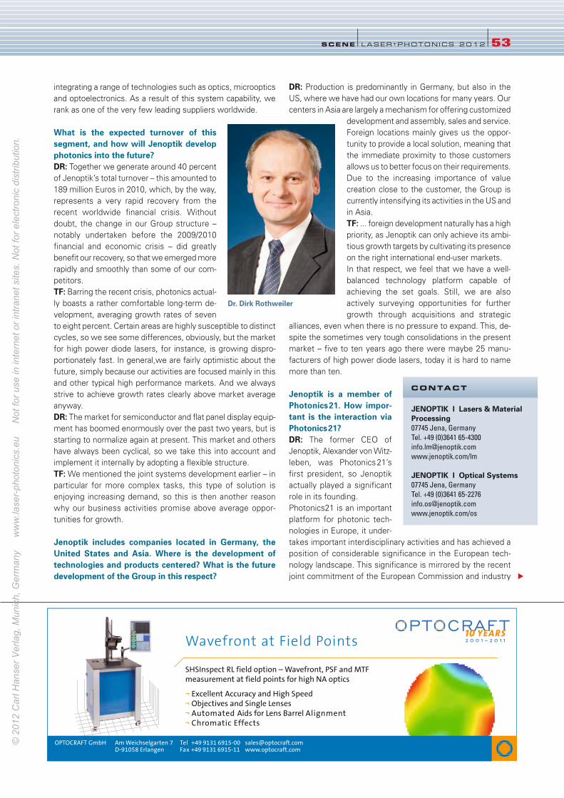
integrating a range of technologies such as optics, microoptics
and optoelectronics. As a result of this system capability, we
rank as one of the very few leading suppliers worldwide.
What is the expected turnover of thissegment, and how will Jenoptik developphotonics into the future? DR: Together we generate around 40 percent
of Jenoptik’s total turnover – this amounted to
189 million Euros in 2010, which, by the way,
represents a very rapid recovery from the
recent worldwide financial crisis. Without
doubt, the change in our Group structure –
notably undertaken before the 2009/2010
financial and economic crisis – did greatly
benefit our recovery, so that we emerged more
rapidly and smoothly than some of our com-
petitors.
TF: Barring the recent crisis, photonics actual-
ly boasts a rather comfortable long-term de-
velopment, averaging growth rates of seven
to eight percent. Certain areas are highly susceptible to distinct
cycles, so we see some differences, obviously, but the market
for high power diode lasers, for instance, is growing dispro-
portionately fast. In general,we are fairly optimistic about the
future, simply because our activities are focused mainly in this
and other typical high performance markets. And we always
strive to achieve growth rates clearly above market average
anyway.
DR: The market for semiconductor and flat panel display equip-
ment has boomed enormously over the past two years, but is
starting to normalize again at present. This market and others
have always been cyclical, so we take this into account and
implement it internally by adopting a flexible structure.
TF: We mentioned the joint systems development earlier – in
particular for more complex tasks, this type of solution is
enjoying increasing demand, so this is then another reason
why our business activities promise above average oppor-
tunities for growth.
Jenoptik includes companies located in Germany, theUnited States and Asia. Where is the development oftechnologies and products centered? What is the futuredevelopment of the Group in this respect?
DR: Production is predominantly in Germany, but also in the
US, where we have had our own locations for many years. Our
centers in Asia are largely a mechanism for offering customized
development and assembly, sales and service.
Foreign locations mainly gives us the oppor-
tunity to provide a local solution, meaning that
the immediate proximity to those customers
allows us to better focus on their requirements.
Due to the increasing importance of value
creation close to the customer, the Group is
currently intensifying its activities in the US and
in Asia.
TF: ... foreign development naturally has a high
priority, as Jenoptik can only achieve its ambi-
tious growth targets by cultivating its presence
on the right international end-user markets.
In that respect, we feel that we have a well-
balanced technology platform capable of
achieving the set goals. Still, we are also
actively surveying opportunities for further
growth through acquisitions and strategic
alliances, even when there is no pressure to expand. This, de-
spite the sometimes very tough consolidations in the present
market – five to ten years ago there were maybe 25 manu-
facturers of high power diode lasers, today it is hard to name
more than ten.
Jenoptik is a member ofPhotonics21. How impor-tant is the interaction viaPhotonics21? DR: The former CEO of
Jenoptik, Alexander von Witz-
leben, was Photonics21’s
first president, so Jenoptik
actually played a significant
role in its founding.
Photonics21 is an important
platform for photonic tech-
nologies in Europe, it under-
takes important interdisciplinary activities and has achieved a
position of considerable significance in the European tech-
nology landscape. This significance is mirrored by the recent
joint commitment of the European Commission and industry
SCENE l LASER+PHOTONICS 2012 l53
JENOPTIK I Lasers & MaterialProcessing07745 Jena, Germany
Tel. +49 (0)3641 65-4300
www.jenoptik.com/lm
JENOPTIK I Optical Systems07745 Jena, Germany
Tel. +49 (0)3641 65-2276
www.jenoptik.com/os
CONTACT
Dr. Dirk Rothweiler
52-55_LPX110134_jenoptik interview_LPex2012 ax 15.12.2011 16:49 Uhr Seite 53
© 2
012
Car
l Han
ser V
erla
g, M
unic
h, G
erm
any
w
ww
.lase
r-ph
oton
ics.
eu
Not
for u
se in
inte
rnet
or i
ntra
net s
ites.
Not
for e
lect
roni
c di
strib
utio
n.

to invest 7 billion Euros in photonics development between
now and 2020. We are and will remain active in the relevant
Work Groups, and we do intensively follow activities and
discuss results internally. All major focal points are correctly
set, in our opinion.
TF:… of course we are pleased to see photonics development
identified by the EC as one of five key enabling technologies
(KETs). In particular the recently published study on the
significance of photonic technologies in Europe [Photonics
Leverage Report, Laser+Photonik 4/2011 and online – Ed.],
on behalf of the European Commission, highlights its role:
Photonics is an interdisciplinary technology which influences
around ten percent of Europe’s overall economic performance!
Jenoptik’s own activities, incidentally, are evident in all of the
identified photonics end-user markets.
What might visitors expect at Photonics West 2012? Howimportant are the leading photonics trade fairs? TF: We will be exhibiting examples from the entire range of
laser sources available from the Lasers & Material Processing
division – this includes semiconductor materials and high
power diode lasers as well as disk and fiber lasers. We will
also be reporting on our novel high power fiber laser and
discussing our road-map for fiber laser develpment, both for
OEMs and for complete turnkey systems.
There are also presentations of medical systems based on the
›JenLas D2‹ femtosecond laser technology, boasting compact
design, optimized beam quality and high power up to 8 W for
ophthalmology and and also for applications in the Show &
Entertainment sector.
DR: In the Optical Systems division we are introducing, for
instance, the new high power ›JENar‹ f-Theta fused silica
lenses for laser material processing developed for laser
powers in the multi-kW range. In general, we are not focusing
on standard products, as we are a strongly customer-oriented
OEM partner and our customers are often market leaders in
their fields. We will thus demonstrate our solution capabilities
and our technology platform, effectively a one-stop-shop for
high precision optical solutions – from optical components all
the way up to integrated optoelectronic solutions, including
software and image processing.
Leading trade fairs such as Photonics West or Laser World of
Photonics, where we jointly exhibit our entire range of tech-
nologies and competency in the field of photonics, remain an
important sector platform to us. But we are also keen to
exhibit at application-specific technical trade fairs, with the
opportunity of convincing customers from specific industries,
markets or regions of our services.
To what extent does Jenoptik support and run programsfor training and development of (junior) staff? TF: We consider this a very important topic, as a highly know-
ledge and experience-dependent industry such as ours relies
heavily on the know-how of its staff. Sustained staff develop-
ment and education programs for young employees are there-
fore very important with regard to the further qualification of
our already well-trained workforce. Company-specific training
is indispensable in this respect.
At the same time, we are also in close cooperation with Schott
and Carl Zeiss, in that we share a joint training center located
in Jena. And we also have specialist internal programs for fur-
ther education, such as the junior management program ›J2LP‹
(Junior to Leadership Program) for targeted development and
promotion of young Jenoptik staff with leadership potential.
DR: We also cooperate closely with network partners – institutes,
universities and polytechnics as well as the local Thuringian
industry. We actively support joint projects, and even altruistic
investments such as the ›Abbe School of Photonics‹, a uni-
versity-run training program offered in English by distinguished
lecturers and focusing on optics and photonics.
We have, of course, also earned a good reputation for ourselves
– Jenoptik is positioned 59th in the ›top 100‹ employer rankings
in the field of natural sciences. That said, and even though
Jenoptik is a strong and attractive company, attracting highly
qualified professional staff still remains a challenge.
Could you please elaborate on medium-term future devel-opments in the divisions: which product and/or techno-logical developments are on the agenda? DR: Ever smaller chip structures are increasingly in demand for
smart phones, tablet computers et cetera. Ongoing develop-
ment of ever higher performing optical and microoptical
systems for lithography and inspection in the semiconductor
industry will thus remain a powerful driver into the future. We
also apply this same know-how in solutions for flat panel dis-
play and laser processing applications. The trend in all of these
fields is towards more durable and higher performance optics
and optical systems, frequently including micro-optics as well.
54 l LASER+PHOTONICS 2 0 12 lSCENE
52-55_LPX110134_jenoptik interview_LPex2012 ax 15.12.2011 16:49 Uhr Seite 54
© 2
012
Car
l Han
ser V
erla
g, M
unic
h, G
erm
any
w
ww
.lase
r-ph
oton
ics.
eu
Not
for u
se in
inte
rnet
or i
ntra
net s
ites.
Not
for e
lect
roni
c di
strib
utio
n.
We additionally see a future in budding optoelectronic markets
such as LED lighting or in the automotive field, for which we
already provide integrated solutions. Regardless of the indus-
try segment, we are always closely aligned to the demands of
our customers, so it remains important to us that future
developments are tackled in partnership with the same.
TF: In the Lasers & Material Processing division, we try to
illustrate planned laser technology development in road-maps.
This incidentally highlights part of our market strategy, namely
the transition of business acquisition from ›push‹ to ›pull‹.
Automotive ranks as the top market sector – that is, plastics,
metals and hybrid materials must all be processed. Processing
systems need lasers to achieve this, in particular high power
fiber and diode direct lasers systems coupled to 200 to 600 µm
fibers. We also envision great potential in the medical field
(aesthetics/treatments), in certain areas of Defense & Securi-
ty and also in photovoltaics. We are furthermore targeting a
greater market share in more complex laaer processing
systems, which can in turn only be realised through adequate
investment in R&D.
Dr. Rothweiler and Dr. Fehn, thank you very much for yourtime. DR & TF: Thank you!
The interview will also appear online on our portal soon, both
in English and in German.
1990 to1993The Trust Agency takes over the state-held VEB Carl Zeiss Jena in
1990. In 1991, the Jena parent company splits to form Carl Zeiss Jena
GmbH and Jenoptik GmbH.
1994 to 1995To develop an operational business, Jenoptik sets up joint enterprises
and acquires companies with established distribution channels and a
global presence, such as Meissner+Wurst GmbH + Co. (later M+W
Zander) in 1994.
1996 to 1997Jenoptik operates as a public company from Jan. 1996. In 1997,
Jenoptik acquires ESW Extel Systems Wedel, which today consti-
tutes a significant component of the Defense & Civil Systems division.
1998 to 2002In June 1998, Jenoptik AG is listed on the Frankfurt stock exchange.
In 1999, Jenoptik acquires Robot Foto and Electronic GmbH (today the
Traffic Solutions division). A year later, Jenoptik takes over the
measurement technology specialists Hommelwerke GmbH (today the
Industrial Metrology division).
2003 to 2006Following the sale of M+W Zander GmbH in May 2006, Jenoptik
focuses on the core business of lasers, optics, sensor systems and
mechatronics. The acquisition in 2006 of industrial metrology
company Etamic S.A. complements this enterprise.
2007 to 2008Start of a comprehensive strategic reorientation in 2007, under the
new management team of Dr. Michael Mertin and Frank Einhellinger.
In 2008, the operational business is bundled into five divisions: Lasers
& Material Processing, Optical Systems, Industrial Metrology, Traffic
Solutions and Defense & Civil Systems.
2009 to 2011Jenoptik increases its global presence, for instance in China, Korea
and Israel and opens a new laser application center in South Korea.
Towards the end of 2010, Jenoptik sells its aerospace business to
EADS Astrium. In June 2011, Jenoptik celebrates its 20th anniversary.
JENOPTIK’S 20 YEAR SUCCESS STORY
LASYS is clearly focused on machines, processesand services, including laser-specific machine sub-systems. Attracting buyers from various industrysectors whilst covering a diverse range of materials,this is our unique trademark.
Present your applications for laser material proces-sing at this unique industry show.
Absolutely focused:The trade fair for laser users
International trade fair forlaser material processing
12 – 14 JUNE 2012 MESSE STUTTGARTwww.lasys-messe.de
Promotional supporter: Accompanying congress:
BMWi sponsorship
of new companies
52-55_LPX110134_jenoptik interview_LPex2012 ax 15.12.2011 16:49 Uhr Seite 55
© 2
012
Car
l Han
ser V
erla
g, M
unic
h, G
erm
any
w
ww
.lase
r-ph
oton
ics.
eu
Not
for u
se in
inte
rnet
or i
ntra
net s
ites.
Not
for e
lect
roni
c di
strib
utio
n.

GREGORY FL INN
The Laser Zentrum Hannover (LZH), the influential Ger-
man institute that develops laser applications across
a wide range of interdisciplinary topics, celebrates
its 25th birthday this year. The institute was founded in June
of 1986, under the auspices of the Lower Saxony Ministry
for Economics, Technology and Transport, and with the goal
of developing the then still relatively untapped laser
applications technology.
Roots dating back to 1985
The founding of the LZH has its roots back in 1985, when the
then Economic Minister of Lower Saxony heard an impressive
talk given by a Prof. Welling from the University of Hannover.
Even though Lower Saxony was, at the time, still largely an agri-
cultural center, the adoption of high technology
as a future building block to the local economic
area was given high priority. Thus, in an effort to
support small and medium-sized companies in
their development and adoption of new laser
technologies, the LZH was founded under the
leadership of Professors Welling, Tönshoff and
Haferkamp, all of the University of Hannover. The
mix of experts in quantum optics, production
technology and materials science, respectively,
proved to be a fortunate one.
Role of the LZH
Since first founded, the role of the LZH was and
indeed continues to be clearly defined. These
include the (for an institute at least) typical roles
of promoting R&D, providing consulting to
companies with the aim of marrying the needs
of industry with the available innovations, and in
providing the community with an adequately
skilled technical workforce. There were, howev-
er, deeper ties to the needs of the region, for
56 l LASER+PHOTONICS 2 0 12 lSCENE
1 The Professors Haferkamp, Welling and Tönshoff founded the LZH 1986 withthe support of the Ministry of Economics of Lower Saxony
From R&D toindustry25TH ANNIVERSARY. A quarter
of a century after it opened, Laser
Zentrum Hannover looks towards future
research in energy, mobility and life
sciences
56-58_LPX110117_lzh_LPex2012 ax 15.12.2011 16:52 Uhr Seite 56
© 2
012
Car
l Han
ser V
erla
g, M
unic
h, G
erm
any
w
ww
.lase
r-ph
oton
ics.
eu
Not
for u
se in
inte
rnet
or i
ntra
net s
ites.
Not
for e
lect
roni
c di
strib
utio
n.

example in supporting the local automotive and aerospace
industries, in providing a firm basis for the growth of the then
still young optical technology industry, and in nurturing an en-
vironment favourable to spin-offs.
Grassroots research for
industrial innovation
As most of the LZH’s projects have their roots in applied indus-
trial research, the resulting economic benefits are evident through
the establishment of 18 spin-off companies since 1986, with a
total of 500 employees. Many of these were founded as a direct
result of the pursuit of projects in a variety of high-tech fields –
lightweight construction in automotive, rail and aerospace
applications, environmental sensing, diagnostic and therapeutic
medical technology, and in the development of highly innovative
laser and optical systems, either industry-capable or for R&D.
The majority of these spin-offs have been created in the past
decade, and include for example the femtosecond laser
micromachining company Micreon (in
2003), solid-state laser specialist neoLASE
(in 2007) and H2B Photonics (in 2005), the
latter a developer of a laser glass cutting
process, that has since been acquired by
Rofin.
But although laser manufacturing is an ob-
vious area of expertise at LZH, it is by no
means the only one. Other recent spin-offs
include Rowiak, developer of a femtosec-
ond laser platform with medical and phar-
maceutical applications, and in July 2010,
the laser-produced nanoparticle manufac-
turer Particular began operations.
Status quo
The LZH is currently involved in more than
100 R&D projects, spanning eight speciality
areas – even for a fully fledged university this
would be worthy record!
SCENE l LASER+PHOTONICS 20 12 l57
56-58_LPX110117_lzh_LPex2012 ax 15.12.2011 16:52 Uhr Seite 57
© 2
012
Car
l Han
ser V
erla
g, M
unic
h, G
erm
any
w
ww
.lase
r-ph
oton
ics.
eu
Not
for u
se in
inte
rnet
or i
ntra
net s
ites.
Not
for e
lect
roni
c di
strib
utio
n.
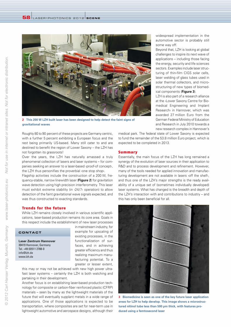
Roughly 80 to 90 percent of these projects are Germany centric,
with a further 5 percent exhibiting a European focus and the
rest being primarily US-based. Many still cater to and are
destined to benefit the region of Lower Saxony – the LZH has
not forgotten its grassroots!
Over the years, the LZH has naturally amassed a truly
phenomenal collection of lasers and laser systems – for com-
panies seeking an answer to a laser-based ›proof-of concept‹,
the LZH thus personifies the proverbial ›one stop shop‹.
Flagship activities include the construction of a 200 W, fre-
quency-stable, narrow linewidth laser (Figure 2) for gravitation
wave detection using high precision interferometry. This laser
must exhibit extreme stability (in ›24/7‹ operation) to allow
detection of the faint gravitational wave signals expected, and
was thus constructed to exacting standards.
Trends for the future
While LZH remains closely involved in various scientific appli-
cations, laser-based production remains its core area. Goals in
this respect include the establishment of new laser processes
in mainstream industry, for
example for upscaling of
existing processes, in the
functionalization of sur-
faces, and in achieving
greater efficiency and thus
realizing maximum manu-
facturing potential. To a
greater or lesser extent,
this may or may not be achieved with new high power ultra-
fast laser systems – certainly the LZH is both watching and
partaking in their development.
Another focus is on establishing laser-based production tech-
nology for composite or carbon-fiber reinforced plastic (CFRP)
materials – seen by many as the lightweight materials of the
future that will eventually supplant metals in a wide range of
applications. One of those applications is expected to be
transportation, where composites are set for near-term use in
lightweight automotive and aerospace designs, although their
widespread implementation in the
automotive sector is probably still
some way off.
Beyond that, LZH is looking at global
challenges to inspire its next wave of
applications – including those facing
the energy, security and life sciences
sectors. Examples include laser struc-
turing of thin-film CIGS solar cells,
laser welding of glass tubes used in
solar thermal collectors, and micro-
structuring of new types of biomed-
ical components (Figure 3).
LZH is also part of a research alliance
at the ›Lower Saxony Centre for Bio-
medical Engineering and Implant
Research‹ in Hannover, which was
awarded 27 million Euro from the
German Federal Ministry of Education
and Research in July 2010 towards a
new research complex in Hannover’s
medical park. The federal state of Lower Saxony is expected
to fund the remainder of the 53.8 million Euro project, which is
expected to be completed in 2013.
Summary
Essentially, the main focus of the LZH has long remained a
synergy of the evolution of laser sources in their application to
R&D and to process development and refinement. However,
many of the tools needed for applied innovation and manufac-
turing development are not available in lasers ›off the shelf‹,
and thus one of the LZH’s major strengths is the ready avail-
ability of a unique set of (sometimes individually developed)
laser systems. What has changed is the breadth and depth of
the LZH’s interaction with and contributions to industry – and
this has only been beneficial for all.
58 l LASER+PHOTONICS 2 0 12 lSCENE
3 Biomedicine is seen as one of the key future laser applicationareas for LZH to help develop. This image shows a microstruc-tured nitinol tube less than 500 µm thick, with features pro-duced using a femtosecond laser
Laser Zentrum Hannover 30419 Hannover, Germany
Tel. +49 (0)511 2788-0
www.lzh.de
CONTACT
2 This 200 W LZH built laser has been designed to help detect the faint signs of gravitational waves
56-58_LPX110117_lzh_LPex2012 ax 15.12.2011 16:52 Uhr Seite 58
© 2
012
Car
l Han
ser V
erla
g, M
unic
h, G
erm
any
w
ww
.lase
r-ph
oton
ics.
eu
Not
for u
se in
inte
rnet
or i
ntra
net s
ites.
Not
for e
lect
roni
c di
strib
utio
n.
COMPANY PROF ILE l59
LASER COMPONENTS GmbHWerner-von-Siemens-Str. 15
82140 Olching, Germany
Phone +49 8142 2864-0
Fax +49 8142 2864-11
www.lasercomponents.com
LASER COMPONENTS USA, Inc.9 River Road
Hudson, NH 03051, USA
Phone +1 603 821 7040
Fax +1 603 821 7041
www.laser-components.com
LASER COMPONENTS UK, Ltd.Goldlay House, 114 Parkway
Chelmsford Essex CM2 7PR
United Kingdom
Phone +44 1245 491 499
Fax +44 1245 491 801
www.lasercomponents.co.uk
LASER COMPONENTS S.A.S.45 Bis Route des Gardes
92190 Meudon, France
Phone +33 1 39 59 52 25
Fax +33 1 39 59 53 50
www.lasercomponents.fr
Manufacturer – Distributor – Partner
LASER COMPONENTS specializes in the de-
velopment, production and sales of com-
ponents and services for laser technology and
optoelectronics and offers one of the largest
product portfolios worldwide. The focus of
the company is clearly the manufacture of
customer-specific products. More than 120
employees worldwide produce and distribute
components.
Our in-house manufacturing capabilities play
an important role in our product portfolio which
comprises avalanche photodiodes and pulsed
laser diodes for rangefinding, laser diode mod-
ules and optical measurement technology, and
the assembly of fibers for e.g. medical appli-
cations.
One of the most important production lines
at LASER COMPONENTS is our optical coat-
ings. High damage thresholds and short
delivery times as well as the ability to cus-
tomize are the traits of our optics. Our high
quality standard, our flexibility, and our fast
response time have made LASER COMPO-
NENTS a trusted name among coating man-
ufacturers.
Expanding this reputation, we added manufac-
turing capabilities for optical substrates in 2008.
Our customers can now enjoy the benefits of
prototypes being delivered within a very short
time.
Since 2010 we also manufacture photon count-
ing modules with the lowest dark count rate
and highest quantum efficiency available on
the market.
Fields of activity– Laser optics
– Fiber optics
– Laser diodes
– Detectors (UV-IR)
– Measurement technology
– Laser accessories
Range of services– Development, production and distribution of
optical and optoelectronic components
– Calibration center for laser power meters
Research & development activities– Thin layers
– Pulsed laser diodes and Si avalanche photo-
diodes for rangefinding applications
– Photon Counting
– Fiber assemblies for medical applications
_FP_LPex2012 14.12.2011 15:56 Uhr Seite 59
© 2
012
Car
l Han
ser V
erla
g, M
unic
h, G
erm
any
w
ww
.lase
r-ph
oton
ics.
eu
Not
for u
se in
inte
rnet
or i
ntra
net s
ites.
Not
for e
lect
roni
c di
strib
utio
n.
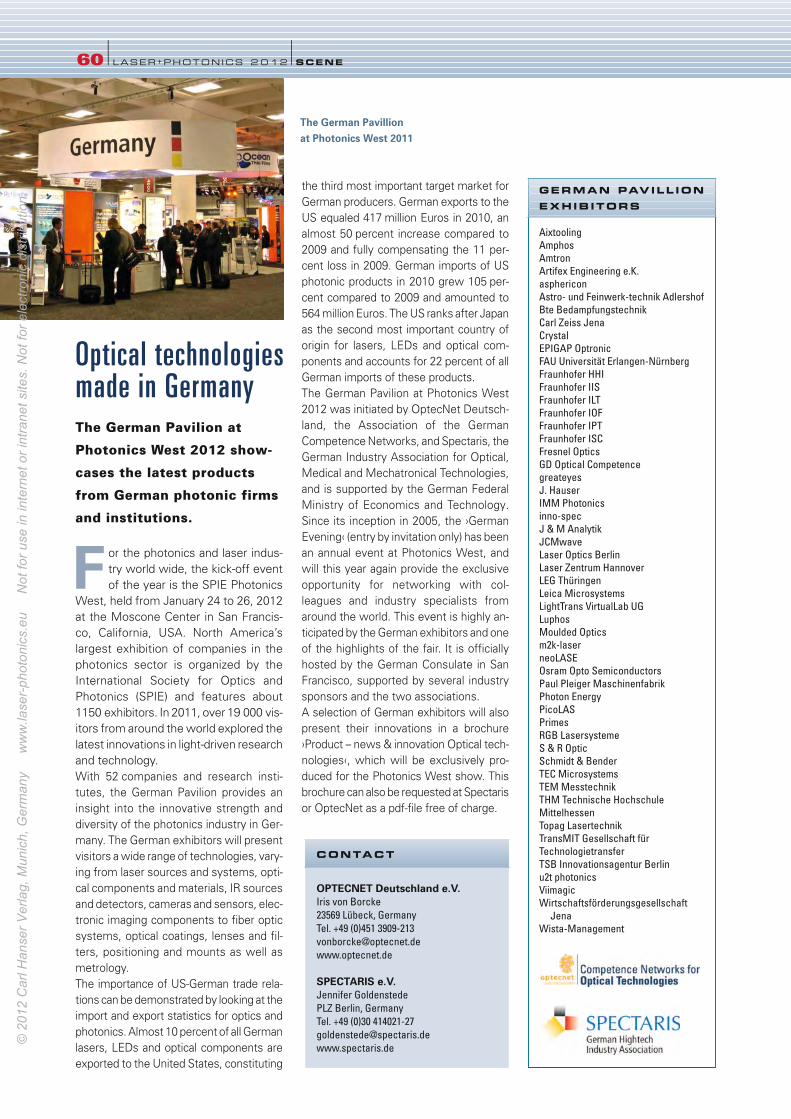
F or the photonics and laser indus-
try world wide, the kick-off event
of the year is the SPIE Photonics
West, held from January 24 to 26, 2012
at the Moscone Center in San Francis-
co, California, USA. North America’s
largest exhibition of companies in the
photonics sector is organized by the
International Society for Optics and
Photonics (SPIE) and features about
1150 exhibitors. In 2011, over 19 000 vis-
itors from around the world explored the
latest innovations in light-driven research
and technology.
With 52 companies and research insti-
tutes, the German Pavilion provides an
insight into the innovative strength and
diversity of the photonics industry in Ger-
many. The German exhibitors will present
visitors a wide range of technologies, vary-
ing from laser sources and systems, opti-
cal components and materials, IR sources
and detectors, cameras and sensors, elec-
tronic imaging components to fiber optic
systems, optical coatings, lenses and fil-
ters, positioning and mounts as well as
metrology.
The importance of US-German trade rela-
tions can be demonstrated by looking at the
import and export statistics for optics and
photonics. Almost 10 percent of all German
lasers, LEDs and optical components are
exported to the United States, constituting
the third most important target market for
German producers. German exports to the
US equaled 417 million Euros in 2010, an
almost 50 percent increase compared to
2009 and fully compensating the 11 per-
cent loss in 2009. German imports of US
photonic products in 2010 grew 105 per-
cent compared to 2009 and amounted to
564 million Euros. The US ranks after Japan
as the second most important country of
origin for lasers, LEDs and optical com-
ponents and accounts for 22 percent of all
German imports of these products.
The German Pavilion at Photonics West
2012 was initiated by OptecNet Deutsch-
land, the Association of the German
Competence Networks, and Spectaris, the
German Industry Association for Optical,
Medical and Mechatronical Technologies,
and is supported by the German Federal
Ministry of Economics and Technology.
Since its inception in 2005, the ›German
Evening‹ (entry by invitation only) has been
an annual event at Photonics West, and
will this year again provide the exclusive
opportunity for networking with col-
leagues and industry specialists from
around the world. This event is highly an-
ticipated by the German exhibitors and one
of the highlights of the fair. It is officially
hosted by the German Consulate in San
Francisco, supported by several industry
sponsors and the two associations.
A selection of German exhibitors will also
present their innovations in a brochure
›Product – news & innovation Optical tech-
nologies‹, which will be exclusively pro-
duced for the Photonics West show. This
brochure can also be requested at Spectaris
or OptecNet as a pdf-file free of charge.
60 l LASER+PHOTONICS 2 0 12 lSCENE
Optical technologiesmade in Germany The German Pavilion at
Photonics West 2012 show-
cases the latest products
from German photonic firms
and institutions.
Aixtooling
Amphos
Amtron
Artifex Engineering e.K.
asphericon
Astro- und Feinwerk-technik Adlershof
Bte Bedampfungstechnik
Carl Zeiss Jena
Crystal
EPIGAP Optronic
FAU Universität Erlangen-Nürnberg
Fraunhofer HHI
Fraunhofer IIS
Fraunhofer ILT
Fraunhofer IOF
Fraunhofer IPT
Fraunhofer ISC
Fresnel Optics
GD Optical Competence
greateyes
J. Hauser
IMM Photonics
inno-spec
J & M Analytik
JCMwave
Laser Optics Berlin
Laser Zentrum Hannover
LEG Thüringen
Leica Microsystems
LightTrans VirtualLab UG
Luphos
Moulded Optics
m2k-laser
neoLASE
Osram Opto Semiconductors
Paul Pleiger Maschinenfabrik
Photon Energy
PicoLAS
Primes
RGB Lasersysteme
S & R Optic
Schmidt & Bender
TEC Microsystems
TEM Messtechnik
THM Technische Hochschule
Mittelhessen
Topag Lasertechnik
TransMIT Gesellschaft für
Technologietransfer
TSB Innovationsagentur Berlin
u2t photonics
Viimagic
Wirtschaftsförderungsgesellschaft
Jena
Wista-Management
GERMAN PAVILL ION
EXHIB ITORS
OPTECNET Deutschland e.V.Iris von Borcke
23569 Lübeck, Germany
Tel. +49 (0)451 3909-213
www.optecnet.de
SPECTARIS e.V.Jennifer Goldenstede
PLZ Berlin, Germany
Tel. +49 (0)30 414021-27
www.spectaris.de
CONTACT
The German Pavillion at Photonics West 2011
60_Spectaris LPex2012_neu_x 15.12.2011 16:54 Uhr Seite 60
© 2
012
Car
l Han
ser V
erla
g, M
unic
h, G
erm
any
w
ww
.lase
r-ph
oton
ics.
eu
Not
for u
se in
inte
rnet
or i
ntra
net s
ites.
Not
for e
lect
roni
c di
strib
utio
n.
COMPANY PROF ILE l61
The Fiber Optics buiness unit of LEONI Group
is one of the leading suppliers of optical fiber
technology for special app0lications in a host
of industrial sectots as well as in science and
medicine. LEONI offers a unique product port-
folio at every stag in the value chain: from the
perform and the fibers drawn from it to fiber-
optic-cables and cable assemblies fitted with
in-house design components. We operate sev-
en production sites troughout Germany.
Learn about product families:
FiberConnect® Light Guide Cable Solutions
We offer you cables with optical fibers made
from glass (singlemode and multimode), plas-
tic optical fibers (POF), plastic cladded fibers
(PCF) and large-core fibers (silica/silica). All fiber
types are also available in a radiation-resistant
version. We manufacture different cable de-
signs from central core cables to breakout ca-
bles with all buffered fiber types and specific
inner and outer jacketing materials, customised
according to your needs. We use all fiber types
to produce hybrid cables with optical fibers and
electrical conductors.
FiberTech® Special Optical Fiber Technologies
We manufacture multimode and singlemode
fibers and fiber bundles with different numer-
ical apertures, coatings and claddings. We spe-
cialise in special fibers and special coatings.
Our company has four optical fiber drawing
towers as well as corresponding screeners
and extruders. All fibers can be assembled to
the customer's specific needs for high-per-
formance laser cables or, for example, spec-
troscopic applications. We manufacture med-
ical fibers for laser energy transmission and
also offer series production of surgical, oph-
thalmological, urological, dental and endovas-
cular laser probes with biocompatible materi-
al.
FiberSwitch® Light Switching for Optical Sys-
tems
Our fiber optical switches are based on a
patented micromechanical/micro-optical de-
sign. This guarantees excellent properties, con-
siderable flexibility and maximum long-term
stability for many applications. The switches
are available for wide wavelength ranges from
the visible to the infrared and for a wide vari-
ety of fiber types. Our switches are designed
for applications with the highest requirements
in the telecommunications area, in measure-
ment and testing and in the biomedical area.
Examples of these complex applications in-
clude spectroscopy, laser scan microscopy,
multi-channel optical performance monitoring,
fiber Bragg sensors, testing of fiber optical ca-
bles and environmental trace analysis.
FiberSplit® Light Distribution for Optical Sys-
tems
Based on optical chip technology, the Fiber-
Split® product portfolio includes standard com-
ponents such as 1xN or 2xN splitters as well
as customised modules or systems with inte-
grated complex functionality for fiber optical
singlemode and multimode systems. Fiber-
Split® products guarantee expandability with
wide optical bandwidth and maximum bit rates
thanks to extremely low PDL/PMD. Our prod-
ucts meet TELCORDIA standards and have
been failure-free in the field for the past 16
years. We also produce customer-specific
chips, components and modules, for example
optical waveguide structures for wavelength
ranges between 600 and 1700 nm with vari-
ous waveguide properties and functions includ-
ing optical chips and fiber arrays.
LEONI Fiber Optics GmbHMühldamm 6
96524 Neuhaus-Schierschnitz
Germany
Phone +49 (0)36764 81100
Fax +49 (0)36764 81110
www.leoni-fiber-optics.com
LEONI Fiber Optics GmbHNalepastrasse 170–171
12459 Berlin
Germany
Phone +49 (0)30 5300580
Fax +49 (0)30 53005858
www.leoni-fiber-optics.com
_FP_LPex2012 14.12.2011 16:00 Uhr Seite 61
© 2
012
Car
l Han
ser V
erla
g, M
unic
h, G
erm
any
w
ww
.lase
r-ph
oton
ics.
eu
Not
for u
se in
inte
rnet
or i
ntra
net s
ites.
Not
for e
lect
roni
c di
strib
utio
n.
62 lCOMPANY PROF ILE
COMPANY PROF ILE
RAYLASE AGArgelsrieder Feld 2+4
82234 Wessling
Germany
Phone +49 (0) 8153 8898-0
Fax +49 (0) 8153 8898-10
RAYLASE AG – TOTAL CONTROL OF YOURLASER BEAMAs a global market leader RAYLASE develops
and manufactures galvanometer-scanner
based components and subsystems for laser
beam deflection, modulation and control. Since
its foundation in April 1999, RAYLASE has been
facing the challenges in this field and supply-
ing the market with innovative, high perform-
ance and quality scan solutions.
DIN EN ISO 9001:2008 standard certified RAY-
LASE offers customized solutions for the in-
creasing requirements of laser technology in
many industries such as automotive, electron-
ics, packaging, textiles, security and solar. In
these industries laser technology is used for
diverse applications like cutting, marking, per-
forating and welding of plastics, metal, glass,
textiles and other materials.
In addition to reliable 2-axis laser beam deflec-
tion units and 3-axis laser beam subsystems,
RAYLASE offers customers the right combina-
tion of application software and control elec-
tronics.
With our subsidiary in Shenzhen, customers
can benefit from our services in mainland Chi-
na and Asia region. In addition to our footprint
in Asia we recently opened a RAYLASE Certi-
fied Service and Repair Center in Sao Paulo,
(Brazil) in 2010; this activity underlines our fo-
cus on the BRIC states (Brazil, Russia, India,
China). Our new center in Brazil acts as an im-
portant hub for South America. Further we
have a RCSC in St. Petersburg together with
our partner Laser Technology Centre.
These RCSCs are able to maintain and repair
all RAYLASE products supplied to each rele-
vant country. International sales are handled
by a worldwide network offering you global
know-how and local expertise.
SCHOTT AGAdvanced Optics
Hattenbergstrasse 10
55122 Mainz
Phone +49 (0)6131 661812
Fax +49 (0)3641 28889047
www.schott.com/advanced_op-tics
SCHOTT AG, Advanced OpticsYour Partner for Excellence in Optics
SCHOTT Advanced Optics, as part of the in-
ternational SCHOTT group, is a valuable part-
ner for its customers in developing products
and customized solutions for applications in
optics, lithography, astronomy, opto-electron-
ics, life sciences, and research. With a global
network of engineering, production and sales,
Advanced Optics offers a portfolio of excellent
products: more than 100 optical glasses, spe-
cial materials, such as active laser glass, IR-
materials and sapphire, ultra-thin glass, high-
precision optical components, wafers, and
optical filters. With more than 125 years of ex-
perience in optics, Advanced Optics masters
the value chain: from customized glass devel-
opment to high-precision optical product fin-
ishing and metrology always reflecting market’
and customer’s needs.
Optical Materials: Optical Glass, Active
Laser Glass, IR-Materials, ZERODUR®, Sap-
phire, Radiation Shielding, B 270®, AF 32®,
D 263®…..
Optical Components: Prisms, Lenses, Wafers
& Substrates, Optical Filter Glass [Color Glass
& Interference Filters]…..
Competences: Processing [Polishing, CNC-
Machining,….], Glass Development, Melting,
Up- and Down-Draw Processes, Coating,
Metrology…..
_FP_LPex2012 14.12.2011 16:00 Uhr Seite 62
© 2
012
Car
l Han
ser V
erla
g, M
unic
h, G
erm
any
w
ww
.lase
r-ph
oton
ics.
eu
Not
for u
se in
inte
rnet
or i
ntra
net s
ites.
Not
for e
lect
roni
c di
strib
utio
n.
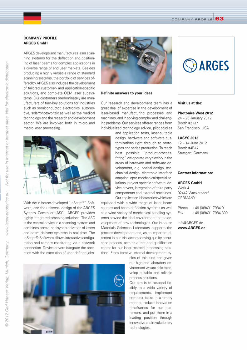
COMPANY PROF ILE l63
Visit us at the:
Photonics West 201224 – 26 January 2012
Booth #2137
San Francisco, USA
LASYS 201212 – 14 June 2012
Booth #4B47
Stuttgart, Germany
Contact Information:
ARGES GmbHWerk 4
92442 Wackersdorf
GERMANY
Phone +49 (0)9431 7984-0
Fax +49 (0)9431 7984-300
www.ARGES.de
COMPANY PROFILEARGES GmbH
ARGES develops and manufactures laser scan-
ning systems for the deflection and position-
ing of laser beams for complex applications in
a diverse range of end user markets. Besides
producing a highly versatile range of standard
scanning systems, the portfolio of services of-
fered by ARGES also includes the development
of tailored customer- and application-specific
solutions, and complete OEM laser subsys-
tems. Our customers predominately are man-
ufacturers of turn-key solutions for industries
such as semiconductor, electronics, automo-
tive, solar/photovoltaic as well as the medical
technology and the research and development
sector. We are involved both in micro and
macro laser processing.
With the in-house developed “InScript©”-Soft-
ware, and the universal design of the ARGES
System Controller (ASC), ARGES provides
highly integrated scanning solutions. The ASC
is the central device in a scanning system and
combines control and synchronization of lasers
and beam delivery systems in real-time. The
InScript©-Software allows interactive configu-
ration and remote monitoring via a network
connection. Device drivers integrate the oper-
ation with the execution of user defined jobs.
Definite answers to your ideas
Our research and development team has a
great deal of expertise in the development of
laser-based manufacturing processes and
machines, and in solving complex and challeng-
ing problems. Our services offered ranges from
individualized technology advice, pilot studies
and application tests, laser-suitable
design, hardware and software cus-
tomizations right through to proto-
types and series production. To reach
best possible “product-process-
fitting” we operate very flexibly in the
areas of hardware and software de-
velopment, e.g. optical design, me-
chanical design, electronic interface
adaption, opto-mechanical special so-
lutions, project-specific software, de-
vice drivers, integration of third-party
components and external machines.
Our application laboratories which are
equipped with a wide range of laser beam
sources and beam deflection systems as well
as a wide variety of mechanical handling sys-
tems provide the ideal environment for the de-
velopment of new technologies. Our in-house
Materials Sciences Laboratory supports the
process development and, as an important el-
ement in our trial-accompanying quality assur-
ance process, acts as a test and qualification
center for our laser material processing solu-
tions. From iterative internal development cy-
cles of this kind and given
our high-end laboratory en-
vironment we are able to de-
velop suitable and reliable
process solutions.
Our aim is to respond fle-
xibly to a wide variety of
requirements, implement
complex tasks in a timely
manner, reduce innovation
timeframes for our cus-
tomers, and put them in a
leading position through
innovative and revolutionary
technologies.
_FP_LPex2012 14.12.2011 16:00 Uhr Seite 63
© 2
012
Car
l Han
ser V
erla
g, M
unic
h, G
erm
any
w
ww
.lase
r-ph
oton
ics.
eu
Not
for u
se in
inte
rnet
or i
ntra
net s
ites.
Not
for e
lect
roni
c di
strib
utio
n.
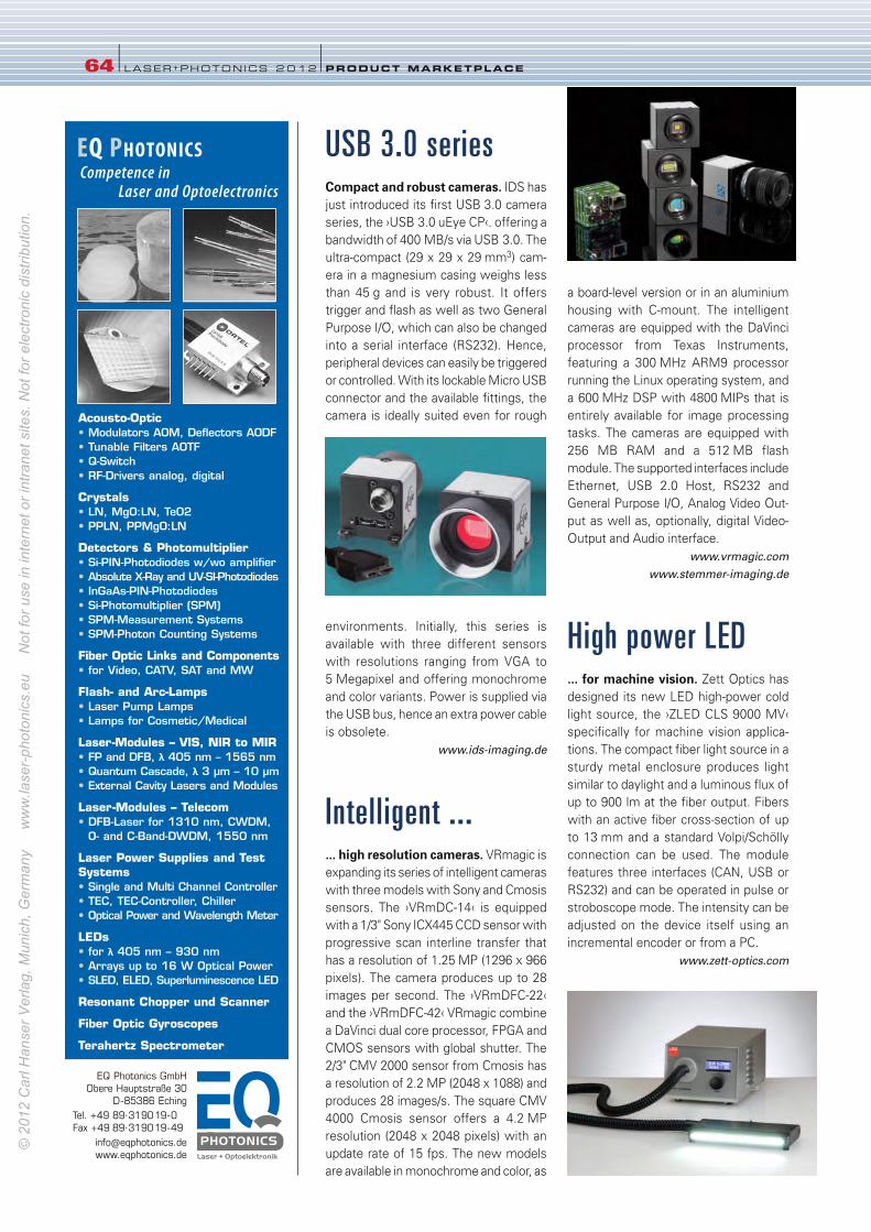
64 l LASER+PHOTONICS 2 0 12 lPRODUCT MARKETPLACE
USB 3.0 seriesCompact and robust cameras. IDS has
just introduced its first USB 3.0 camera
series, the ›USB 3.0 uEye CP‹. offering a
bandwidth of 400 MB/s via USB 3.0. The
ultra-compact (29 x 29 x 29 mm3) cam-
era in a magnesium casing weighs less
than 45 g and is very robust. It offers
trigger and flash as well as two General
Purpose I/O, which can also be changed
into a serial interface (RS232). Hence,
peripheral devices can easily be triggered
or controlled. With its lockable Micro USB
connector and the available fittings, the
camera is ideally suited even for rough
environments. Initially, this series is
available with three different sensors
with resolutions ranging from VGA to
5 Megapixel and offering monochrome
and color variants. Power is supplied via
the USB bus, hence an extra power cable
is obsolete.
www.ids-imaging.de
Intelligent ...... high resolution cameras. VRmagic is
expanding its series of intelligent cameras
with three models with Sony and Cmosis
sensors. The ›VRmDC-14‹ is equipped
with a 1/3" Sony ICX445 CCD sensor with
progressive scan interline transfer that
has a resolution of 1.25 MP (1296 x 966
pixels). The camera produces up to 28
images per second. The ›VRmDFC-22‹
and the ›VRmDFC-42‹ VRmagic combine
a DaVinci dual core processor, FPGA and
CMOS sensors with global shutter. The
2/3" CMV 2000 sensor from Cmosis has
a resolution of 2.2 MP (2048 x 1088) and
produces 28 images/s. The square CMV
4000 Cmosis sensor offers a 4.2 MP
resolution (2048 x 2048 pixels) with an
update rate of 15 fps. The new models
are available in monochrome and color, as
a board-level version or in an aluminium
housing with C-mount. The intelligent
cameras are equipped with the DaVinci
processor from Texas Instruments,
featuring a 300 MHz ARM9 processor
running the Linux operating system, and
a 600 MHz DSP with 4800 MIPs that is
entirely available for image processing
tasks. The cameras are equipped with
256 MB RAM and a 512 MB flash
module. The supported interfaces include
Ethernet, USB 2.0 Host, RS232 and
General Purpose I/O, Analog Video Out-
put as well as, optionally, digital Video-
Output and Audio interface.
www.vrmagic.comwww.stemmer-imaging.de
High power LED... for machine vision. Zett Optics has
designed its new LED high-power cold
light source, the ›ZLED CLS 9000 MV‹
specifically for machine vision applica-
tions. The compact fiber light source in a
sturdy metal enclosure produces light
similar to daylight and a luminous flux of
up to 900 lm at the fiber output. Fibers
with an active fiber cross-section of up
to 13 mm and a standard Volpi/Schölly
connection can be used. The module
features three interfaces (CAN, USB or
RS232) and can be operated in pulse or
stroboscope mode. The intensity can be
adjusted on the device itself using an
incremental encoder or from a PC.
www.zett-optics.com
EQ PHOTONICSCompetence in Laser and Optoelectronics
EQ Photonics GmbH Obere Hauptstraße 30
D-85386 Eching Tel. +49 89·319019-0 Fax +49 89·319019-49
[email protected] www.eqphotonics.de
Acousto-Optic Modulators AOM, Deflectors AODF Tunable Filters AOTF Q-Switch RF-Drivers analog, digital
Crystals LN, MgO:LN, TeO2 PPLN, PPMgO:LN
Detectors & Photomultiplier Si-PIN-Photodiodes w/wo amplifier Absolute X-Ray and UV-SI-Photodiodes InGaAs-PIN-Photodiodes Si-Photomultiplier (SPM) SPM-Measurement Systems SPM-Photon Counting Systems
Fiber Optic Links and Components for Video, CATV, SAT and MW
Flash- and Arc-Lamps Laser Pump Lamps Lamps for Cosmetic/Medical
Laser-Modules – VIS, NIR to MIR FP and DFB, λ 405 nm – 1565 nm Quantum Cascade, λ 3 μm – 10 μm External Cavity Lasers and Modules
Laser-Modules – Telecom DFB-Laser for 1310 nm, CWDM,
O- and C-Band-DWDM, 1550 nm
Laser Power Supplies and Test Systems Single and Multi Channel Controller TEC, TEC-Controller, Chiller Optical Power and Wavelength Meter
LEDs for λ 405 nm – 930 nm Arrays up to 16 W Optical Power SLED, ELED, Superluminescence LED
Resonant Chopper und Scanner
Fiber Optic Gyroscopes
Terahertz Spectrometer
64-65_produkte_LPex2012_x 15.12.2011 16:59 Uhr Seite 64
© 2
012
Car
l Han
ser V
erla
g, M
unic
h, G
erm
any
w
ww
.lase
r-ph
oton
ics.
eu
Not
for u
se in
inte
rnet
or i
ntra
net s
ites.
Not
for e
lect
roni
c di
strib
utio
n.

PRODUCT MARKETPLACE l LASER+PHOTONICS 2012 l65
CoaxPress interfaceHigh speed camera. Optronis has pre-
sented its first 4 MP camera with a Coax-
Press interface, claiming it to be the
world’s first 4 MP CoaxPress high speed
camera. The ›CL4000CXP‹ allows up to
500 fps to be transferred to a PC in real
time. The CoaxPress interface’s serial
transmission concept enables data to be
transferred at a gross clock frequency of
up to 6.25 Gbit/s via a single coaxial ca-
ble, or using multiple 75 W coaxial cables
if the transmission capacity is upscaled.
Key advantages of CoaxPress include its
scalability and transmission distances of
up to 100 m. The image data is processed
using CoaxPress frame grabbers de-
signed for simultaneous processing of
four data channels. The high speed data
transfer makes the CL4000CXP suitable
for many kinds of applications, including
2D and 3D shots in wafer or solar cell
production, video data streaming and
OEM applications.
www.optronis.com
COS4-corrected Laser for machine vision. Laser 2000
offers a COS4-corrected laser, which
helps avoid the vignetting that occurs in
laser systems with cylinder lenses, par-
ticularly with a larger field of view. The
special optical grinding compensates for
overexposure in the center of the image,
which can be as much as 40 percent with
a 90° laser, and ensures that only ap-
proximately 25 percent of the output is
visible at the ends of the lines. This com-
pensation for the COS4 effect enables
the lasers to generate lines of maximum
homogeneity and projections with the
greatest possible uniformity in their
intensity. www.laser2000.de
Wir produzieren hochpräzise feinmecha-
nische CNC-Drehteile, -Frästeile und draht-
erodierte Teile für die unterschiedlichsten
Bereiche der Medizintechnik, Sensorik,
Mess- und Regeltechnik.
We manufacture mechanical and preci-sion engineering CNC-turned and -milled parts as well as wire-eroded parts for a variety of applications including medical technology,sensor systems, measuring and control technology.
Helmut Klingel GmbH · CNC-Zerspanung
Hanauer Straße 5-7 · 75181 Pforzheim (Germany)
Telefon +49 7231 6519-0 · Telefax +49 7231 6519-71
www.klingel-cnc.de · [email protected]
Einzigartig in der Vielfalt
Unique in diversity
Small, powerful, nearly indestructibleIndustrial cameras. A range of ECO series cameras from SVS Vistek are now avail-
able in a watertight and exceptionally durable design called ›BlackLine‹ version. The
enclosure has IP67 protection and is totally HF and moisture proof. The C-mount lens
connection is sealed and a lens barrel compatible with most compact lenses provides
additional protection against environmental influences. The M12 connector from Phoenix
Contact complies with the requirements for protection class IP67 and allows rapid and
cost-effective cabling. Three inputs, three outputs (two with high current LED driver)
and an RS 232 Ethernet interface are provided. The supply voltage is industry compli-
ant at up to 24 V DC ±20 percent. A variety of different trigger modes enable almost
any conceivable system configuration. The new ›Logic Trigger‹ allows multiple inputs
on the camera to be linked using logic functions, for example rotary encoders and light
barriers. Two LED lighting systems can now be controlled directly. The ECO sequence
shutter and LED control functions provide exposure combinations that allow almost any
test specimen to be optimally analyzed. Ten sensor resolutions from VGA to 5 MP will
be available in monochrome or color design, making the ECO BlackLine ideal for use
in automation and in the transport and medical sectors. www.svs-vistek.com
64-65_produkte_LPex2012_x 15.12.2011 16:59 Uhr Seite 65
© 2
012
Car
l Han
ser V
erla
g, M
unic
h, G
erm
any
w
ww
.lase
r-ph
oton
ics.
eu
Not
for u
se in
inte
rnet
or i
ntra
net s
ites.
Not
for e
lect
roni
c di
strib
utio
n.
PETER VON JAN
MARKUS AXTNER
High brightness lasers often enable higher processing
speeds that simply cannot be matched with stan-
dard movement systems. Galvanometer scanner
systems that have been used successfully for many years,
in particular in the marking sector, offer here the only alter-
native to the traditional multi-axial systems. It is, however,
inherent to the operating principle of a scanner that even the
smallest angle deviation of the scanner motors can have a
dramatic impact on the position of the laser focus in the
processing plane, in particular because relatively large
processing distances can be used.
A new high-precision scanner generation is thus required that
continuously shows the same stable performance under all
operating conditions (deflection speed, duty cycle) in the long-
term, and that additionally offers higher maximum performance
and greater dynamic range for these operating conditions
compared with previous generations. The new ›Superscan-II‹
by Raylase fulfils all of these requirements perfectly.
The new Superscan-II
The new scan head (pictured above) is a compact unit quali-
fied for high demand applications with regard to precision and
long-term stability. At apertures of 10, 15, 20 und 30 mm,
66 l LASER+PHOTONICS 2 0 12 lMATERIALS PROCESSING
More precise beam deflection NEW HIGH-PRECISION SCANHEADS. With the increasing use of
high brightness lasers on the one hand
and the increasing complexity of produc-
tion processes on the other, end-users
require increasingly higher precision
with regard to processing optics and
beam positioning.
Laser Nd:YAG Nd: YAG doubled
Nd: YAG tripledt Broadband Diode lasers CO2
Wavelength (nm) 1064 532 355 400-1064 800-980 10600 10600
Coating dielectric dielectric dielectric silver IP dielectric dielectric dielectric
Min. reflection @ wavelength (nm)
99.5% @ 106480.0% @ 633
99.5% @ 53250.0% @ 633
99.0% @ 35580.0% @ 633
97.0% @ 400-106497.0% @ 633
99.0% @ 808-98050.0% @ 633
99.9% @ 1060080.0% @ 450-650
99.0% @ 1060080.0% @ 450-650
Flatness - 633 nm l/4 l/4 l/4 l/4 l/4 l/4 l/4
Max. laser power, cw (W/cm2) 500 500 100 70 500 500 80
Max. laser power,100 ns pulse width(MW/cm2)
100 100 (10 ns) 20 (10 ns) N/A N/A 400 400
Scratch & dig 40/20 40/20 40/20 40/20 40/20 40/20 40/20
A Mirror specifications for the Superscan-II
66-68_LPX110017_raylase_LPex2012 ax 15.12.2011 17:02 Uhr Seite 66
© 2
012
Car
l Han
ser V
erla
g, M
unic
h, G
erm
any
w
ww
.lase
r-ph
oton
ics.
eu
Not
for u
se in
inte
rnet
or i
ntra
net s
ites.
Not
for e
lect
roni
c di
strib
utio
n.
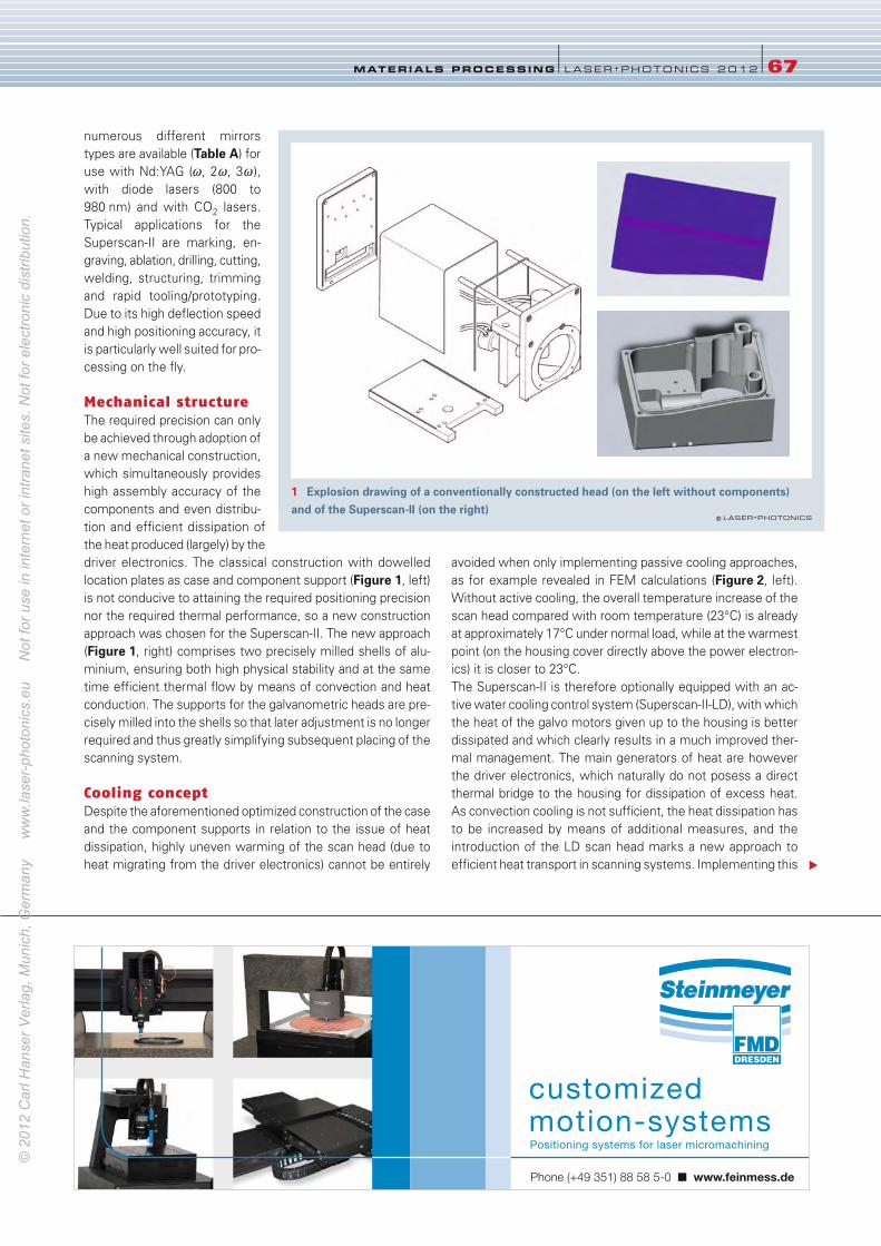
Phone (+49 351) 88 58 5-0 www.feinmess.de
customizedmotion-systemsPositioning systems for laser micromachining
numerous different mirrors
types are available (Table A) for
use with Nd:YAG (v, 2v, 3v),
with diode lasers (800 to
980 nm) and with CO2 lasers.
Typical applications for the
Superscan-II are marking, en-
graving, ablation, drilling, cutting,
welding, structuring, trimming
and rapid tooling/prototyping.
Due to its high deflection speed
and high positioning accuracy, it
is particularly well suited for pro-
cessing on the fly.
Mechanical structure
The required precision can only
be achieved through adoption of
a new mechanical construction,
which simultaneously provides
high assembly accuracy of the
components and even distribu-
tion and efficient dissipation of
the heat produced (largely) by the
driver electronics. The classical construction with dowelled
location plates as case and component support (Figure 1, left)
is not conducive to attaining the required positioning precision
nor the required thermal performance, so a new construction
approach was chosen for the Superscan-II. The new approach
(Figure 1, right) comprises two precisely milled shells of alu-
minium, ensuring both high physical stability and at the same
time efficient thermal flow by means of convection and heat
conduction. The supports for the galvanometric heads are pre-
cisely milled into the shells so that later adjustment is no longer
required and thus greatly simplifying subsequent placing of the
scanning system.
Cooling concept
Despite the aforementioned optimized construction of the case
and the component supports in relation to the issue of heat
dissipation, highly uneven warming of the scan head (due to
heat migrating from the driver electronics) cannot be entirely
avoided when only implementing passive cooling approaches,
as for example revealed in FEM calculations (Figure 2, left).
Without active cooling, the overall temperature increase of the
scan head compared with room temperature (23°C) is already
at approximately 17°C under normal load, while at the warmest
point (on the housing cover directly above the power electron-
ics) it is closer to 23°C.
The Superscan-II is therefore optionally equipped with an ac-
tive water cooling control system (Superscan-II-LD), with which
the heat of the galvo motors given up to the housing is better
dissipated and which clearly results in a much improved ther-
mal management. The main generators of heat are however
the driver electronics, which naturally do not posess a direct
thermal bridge to the housing for dissipation of excess heat.
As convection cooling is not sufficient, the heat dissipation has
to be increased by means of additional measures, and the
introduction of the LD scan head marks a new approach to
efficient heat transport in scanning systems. Implementing this
MATERIALS PROCESSING l LASER+PHOTONICS 2012 l67
1 Explosion drawing of a conventionally constructed head (on the left without components)and of the Superscan-II (on the right)
© LASER+PHOTONICS
66-68_LPX110017_raylase_LPex2012 ax 15.12.2011 17:03 Uhr Seite 67
© 2
012
Car
l Han
ser V
erla
g, M
unic
h, G
erm
any
w
ww
.lase
r-ph
oton
ics.
eu
Not
for u
se in
inte
rnet
or i
ntra
net s
ites.
Not
for e
lect
roni
c di
strib
utio
n.
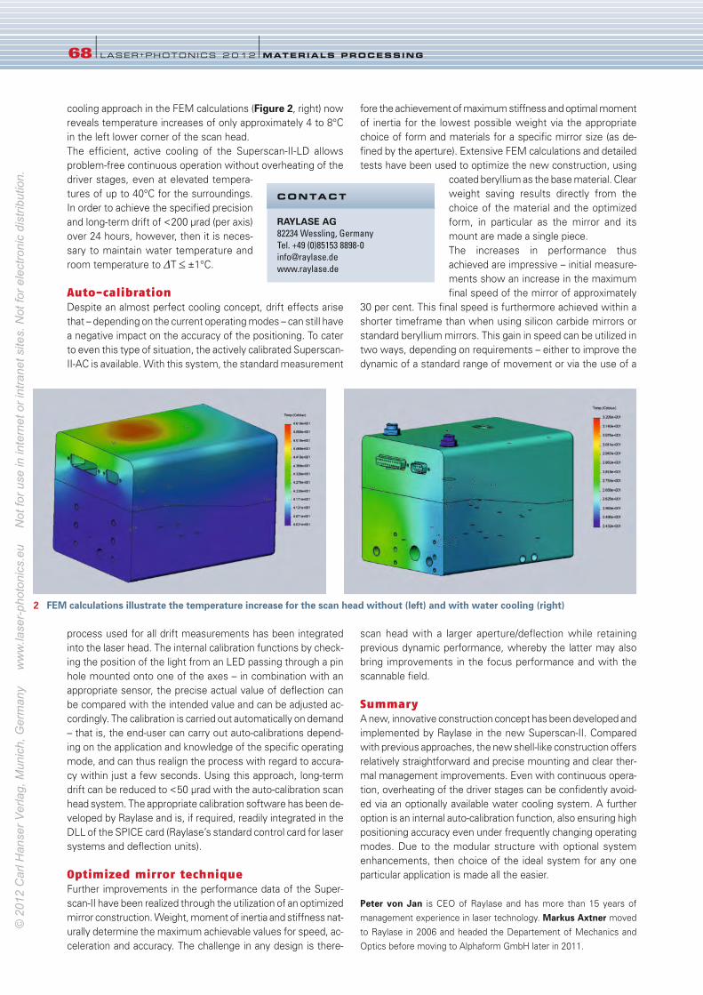
cooling approach in the FEM calculations (Figure 2, right) now
reveals temperature increases of only approximately 4 to 8°C
in the left lower corner of the scan head.
The efficient, active cooling of the Superscan-II-LD allows
problem-free continuous operation without overheating of the
driver stages, even at elevated tempera-
tures of up to 40°C for the surroundings.
In order to achieve the specified precision
and long-term drift of <200 µrad (per axis)
over 24 hours, however, then it is neces-
sary to maintain water temperature and
room temperature to DT≤±1°C.
Auto-calibration
Despite an almost perfect cooling concept, drift effects arise
that – depending on the current operating modes – can still have
a negative impact on the accuracy of the positioning. To cater
to even this type of situation, the actively calibrated Superscan-
II-AC is available. With this system, the standard measurement
process used for all drift measurements has been integrated
into the laser head. The internal calibration functions by check-
ing the position of the light from an LED passing through a pin
hole mounted onto one of the axes – in combination with an
appropriate sensor, the precise actual value of deflection can
be compared with the intended value and can be adjusted ac-
cordingly. The calibration is carried out automatically on demand
– that is, the end-user can carry out auto-calibrations depend-
ing on the application and knowledge of the specific operating
mode, and can thus realign the process with regard to accura-
cy within just a few seconds. Using this approach, long-term
drift can be reduced to <50 µrad with the auto-calibration scan
head system. The appropriate calibration software has been de-
veloped by Raylase and is, if required, readily integrated in the
DLL of the SPICE card (Raylase’s standard control card for laser
systems and deflection units).
Optimized mirror technique
Further improvements in the performance data of the Super-
scan-II have been realized through the utilization of an optimized
mirror construction. Weight, moment of inertia and stiffness nat-
urally determine the maximum achievable values for speed, ac-
celeration and accuracy. The challenge in any design is there-
fore the achievement of maximum stiffness and optimal moment
of inertia for the lowest possible weight via the appropriate
choice of form and materials for a specific mirror size (as de-
fined by the aperture). Extensive FEM calculations and detailed
tests have been used to optimize the new construction, using
coated beryllium as the base material. Clear
weight saving results directly from the
choice of the material and the optimized
form, in particular as the mirror and its
mount are made a single piece.
The increases in performance thus
achieved are impressive – initial measure-
ments show an increase in the maximum
final speed of the mirror of approximately
30 per cent. This final speed is furthermore achieved within a
shorter timeframe than when using silicon carbide mirrors or
standard beryllium mirrors. This gain in speed can be utilized in
two ways, depending on requirements – either to improve the
dynamic of a standard range of movement or via the use of a
scan head with a larger aperture/deflection while retaining
previous dynamic performance, whereby the latter may also
bring improvements in the focus performance and with the
scannable field.
Summary
A new, innovative construction concept has been developed and
implemented by Raylase in the new Superscan-II. Compared
with previous approaches, the new shell-like construction offers
relatively straightforward and precise mounting and clear ther-
mal management improvements. Even with continuous opera-
tion, overheating of the driver stages can be confidently avoid-
ed via an optionally available water cooling system. A further
option is an internal auto-calibration function, also ensuring high
positioning accuracy even under frequently changing operating
modes. Due to the modular structure with optional system
enhancements, then choice of the ideal system for any one
particular application is made all the easier.
Peter von Jan is CEO of Raylase and has more than 15 years of
management experience in laser technology. Markus Axtner moved
to Raylase in 2006 and headed the Departement of Mechanics and
Optics before moving to Alphaform GmbH later in 2011.
68 l LASER+PHOTONICS 2 0 12 lMATERIALS PROCESSING
RAYLASE AG 82234 Wessling, Germany
Tel. +49 (0)85153 8898-0
www.raylase.de
CONTACT
2 FEM calculations illustrate the temperature increase for the scan head without (left) and with water cooling (right)
66-68_LPX110017_raylase_LPex2012 ax 15.12.2011 17:03 Uhr Seite 68
© 2
012
Car
l Han
ser V
erla
g, M
unic
h, G
erm
any
w
ww
.lase
r-ph
oton
ics.
eu
Not
for u
se in
inte
rnet
or i
ntra
net s
ites.
Not
for e
lect
roni
c di
strib
utio
n.
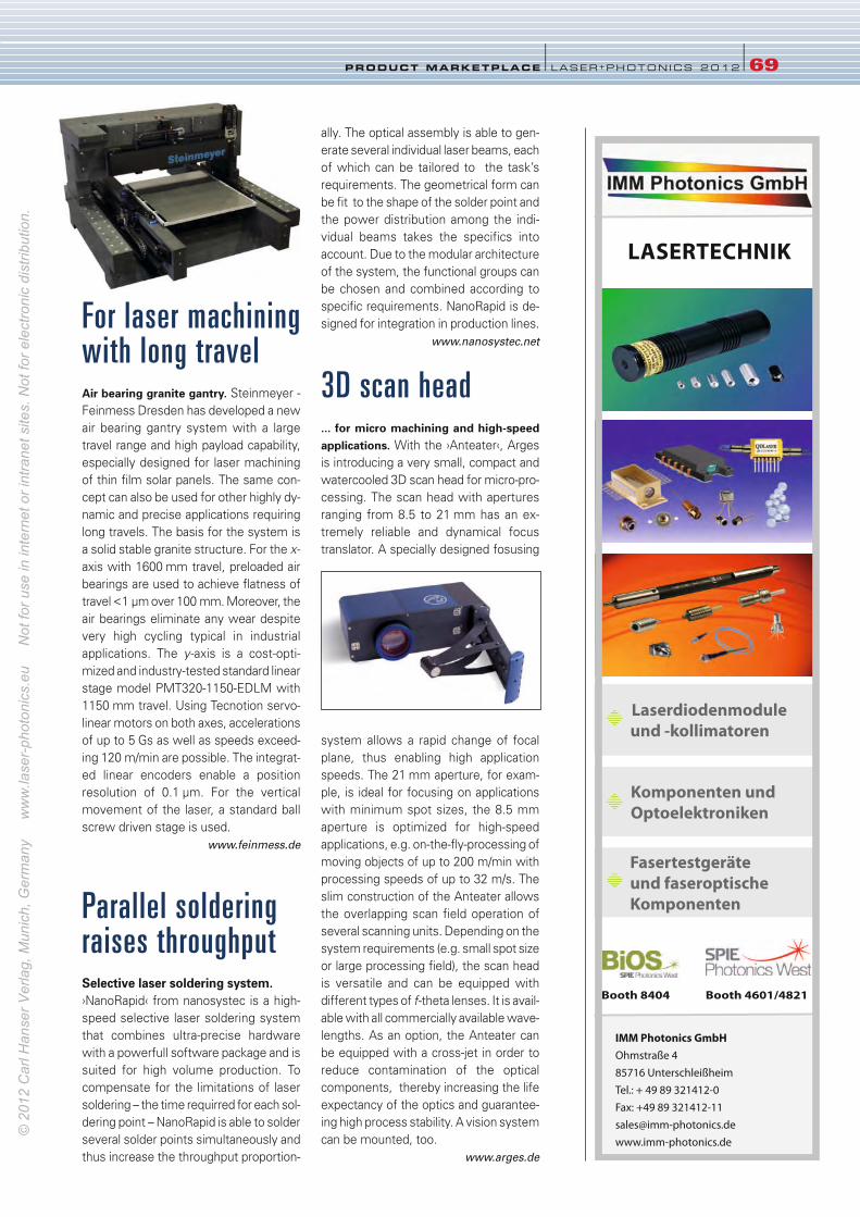
PRODUCT MARKETPLACE l LASER+PHOTONICS 2012 l69
IMM Photonics GmbHOhmstraße 485716 UnterschleißheimTel.: + 49 89 321412-0Fax: +49 89 [email protected]
LASERTECHNIK
Laserdiodenmodule und -kollimatorenLaserdiodenmodule
und -kollimatoren
Komponenten und Optoelektroniken
Fasertestgeräte und faseroptische Komponenten
Booth 8404 Booth 4601/4821
For laser machiningwith long travelAir bearing granite gantry. Steinmeyer -
Feinmess Dresden has developed a new
air bearing gantry system with a large
travel range and high payload capability,
especially designed for laser machining
of thin film solar panels. The same con-
cept can also be used for other highly dy-
namic and precise applications requiring
long travels. The basis for the system is
a solid stable granite structure. For the x-
axis with 1600 mm travel, preloaded air
bearings are used to achieve flatness of
travel <1 µm over 100 mm. Moreover, the
air bearings eliminate any wear despite
very high cycling typical in industrial
applications. The y-axis is a cost-opti-
mized and industry-tested standard linear
stage model PMT320-1150-EDLM with
1150 mm travel. Using Tecnotion servo-
linear motors on both axes, accelerations
of up to 5 Gs as well as speeds exceed-
ing 120 m/min are possible. The integrat-
ed linear encoders enable a position
resolution of 0.1 µm. For the vertical
movement of the laser, a standard ball
screw driven stage is used.
www.feinmess.de
Parallel solderingraises throughput Selective laser soldering system.›NanoRapid‹ from nanosystec is a high-
speed selective laser soldering system
that combines ultra-precise hardware
with a powerfull software package and is
suited for high volume production. To
compensate for the limitations of laser
soldering – the time requirred for each sol-
dering point – NanoRapid is able to solder
several solder points simultaneously and
thus increase the throughput proportion-
ally. The optical assembly is able to gen-
erate several individual laser beams, each
of which can be tailored to the task’s
requirements. The geometrical form can
be fit to the shape of the solder point and
the power distribution among the indi-
vidual beams takes the specifics into
account. Due to the modular architecture
of the system, the functional groups can
be chosen and combined according to
specific requirements. NanoRapid is de-
signed for integration in production lines.
www.nanosystec.net
3D scan head ... for micro machining and high-speedapplications. With the ›Anteater‹, Arges
is introducing a very small, compact and
watercooled 3D scan head for micro-pro-
cessing. The scan head with apertures
ranging from 8.5 to 21 mm has an ex-
tremely reliable and dynamical focus
translator. A specially designed fosusing
system allows a rapid change of focal
plane, thus enabling high application
speeds. The 21 mm aperture, for exam-
ple, is ideal for focusing on applications
with minimum spot sizes, the 8.5 mm
aperture is optimized for high-speed
applications, e.g. on-the-fly-processing of
moving objects of up to 200 m/min with
processing speeds of up to 32 m/s. The
slim construction of the Anteater allows
the overlapping scan field operation of
several scanning units. Depending on the
system requirements (e.g. small spot size
or large processing field), the scan head
is versatile and can be equipped with
different types of f-theta lenses. It is avail-
able with all commercially available wave-
lengths. As an option, the Anteater can
be equipped with a cross-jet in order to
reduce contamination of the optical
components, thereby increasing the life
expectancy of the optics and guarantee-
ing high process stability. A vision system
can be mounted, too.
www.arges.de
69_produkte_LPex2012_x 15.12.2011 17:04 Uhr Seite 69
© 2
012
Car
l Han
ser V
erla
g, M
unic
h, G
erm
any
w
ww
.lase
r-ph
oton
ics.
eu
Not
for u
se in
inte
rnet
or i
ntra
net s
ites.
Not
for e
lect
roni
c di
strib
utio
n.

CHRISTOPH
RÜTT IMANN
ULR ICH DÜRR
Aprerequisite for thermal
laser material process-
ing is direct interaction
between the focused laser radi-
ation and the copper surface.
This then requires part of the
radiation to be absorbed at the
copper surface. As Figure 1shows, however, for a polished
copper surface at room temper-
ature, less than five percent of
the laser radiation is absorbed (at
1 µm wavelength).
Despite this problem, there are a
range of measures that can be
taken to allow copper to be welded successfully and effi-
ciently, particularly with solid-state or fiber lasers. The first of
these measures is coating the surface with more absorbent
materials, such as nickel or chromium. Mechanical prepara-
tion of the surface, for example roughening or painting, also
increases the absorption. However, both of these measures
have a negative impact on production costs, as they require
additional fabrication steps. Chemical impurities can also in-
fluence absorption behavior and thus make it more difficult to
achieve a reproducible welding process.
As can be seen from the absorption curve, shorter wavelengths
would be an advantage. Diode lasers (0.8 to 1 µm, IR) or a
frequency-doubled Nd:YAG laser (532 nm, green), for exam-
ple, can deliver these wavelengths, although neither of these
lasers has yet reached the stage where copper welding would
be industrially viable.
Heating at the point of incidence of the laser radiation is faster
or slower depending on the level of absorption, and the risk of
overheating and splatter formation becomes unpredictable.
The problem of poor reproducibility is even more pronounced
for spot welding than for seam welding. Each
individual laser pulse strikes the cold copper
material and thus experiences different
initial conditions. However, because the ab-
sorption depends not only on the wavelength
and the surface characteristics, but also on
the material temperature (absorption im-
proves significantly at increased tempera-
tures) and the intensity of the laser radiation,
there is additional scope for improving the
welding process.
Overlaying two wavelengths
The poor reproducibility of copper welding
can be significantly improved by overlaying
a laser pulse with a wavelength of 532 nm
on to a laser pulse with a wavelength of
1 µm. If the two laser beams are focused
using the same chromatically compensated
70 l LASER+PHOTONICS 2 0 12 lMATERIALS PROCESSING
Efficient laser welding of copperREPRODUCIBLE COPPER WELDING. Compared to other metals,
laser welding of copper materials is still a major challenge in industrial processing,
in particular in terms of process efficiency and reproducibility.
1 Wavelength dependency of copper absorptivity © LASER+PHOTONICS
2 Comparison of infrared, green and a combination of both wavelengths
70-72_LPX110018_rofinlasag_LPex2012 ax 15.12.2011 17:07 Uhr Seite 70
© 2
012
Car
l Han
ser V
erla
g, M
unic
h, G
erm
any
w
ww
.lase
r-ph
oton
ics.
eu
Not
for u
se in
inte
rnet
or i
ntra
net s
ites.
Not
for e
lect
roni
c di
strib
utio
n.
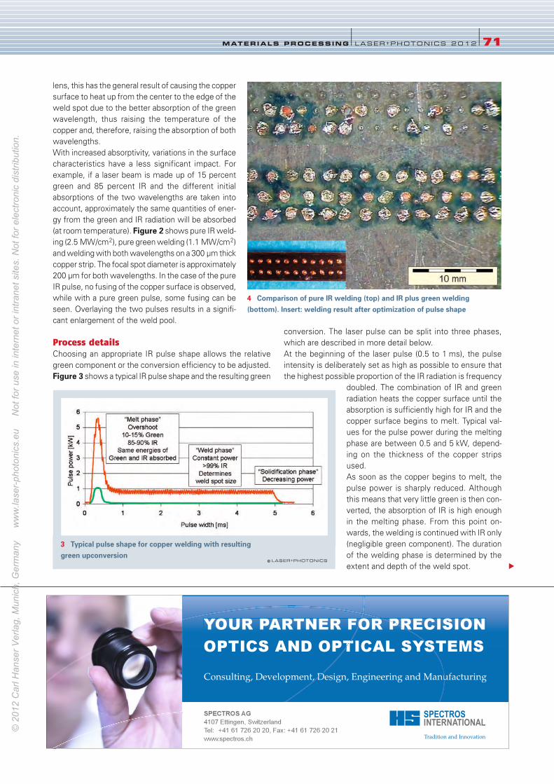
lens, this has the general result of causing the copper
surface to heat up from the center to the edge of the
weld spot due to the better absorption of the green
wavelength, thus raising the temperature of the
copper and, therefore, raising the absorption of both
wavelengths.
With increased absorptivity, variations in the surface
characteristics have a less significant impact. For
example, if a laser beam is made up of 15 percent
green and 85 percent IR and the different initial
absorptions of the two wavelengths are taken into
account, approximately the same quantities of ener-
gy from the green and IR radiation will be absorbed
(at room temperature). Figure 2 shows pure IR weld-
ing (2.5 MW/cm2), pure green welding (1.1 MW/cm2)
and welding with both wavelengths on a 300 µm thick
copper strip. The focal spot diameter is approximately
200 µm for both wavelengths. In the case of the pure
IR pulse, no fusing of the copper surface is observed,
while with a pure green pulse, some fusing can be
seen. Overlaying the two pulses results in a signifi-
cant enlargement of the weld pool.
Process details
Choosing an appropriate IR pulse shape allows the relative
green component or the conversion efficiency to be adjusted.
Figure 3 shows a typical IR pulse shape and the resulting green
conversion. The laser pulse can be split into three phases,
which are described in more detail below.
At the beginning of the laser pulse (0.5 to 1 ms), the pulse
intensity is deliberately set as high as possible to ensure that
the highest possible proportion of the IR radiation is frequency
doubled. The combination of IR and green
radiation heats the copper surface until the
absorption is sufficiently high for IR and the
copper surface begins to melt. Typical val-
ues for the pulse power during the melting
phase are between 0.5 and 5 kW, depend-
ing on the thickness of the copper strips
used.
As soon as the copper begins to melt, the
pulse power is sharply reduced. Although
this means that very little green is then con-
verted, the absorption of IR is high enough
in the melting phase. From this point on-
wards, the welding is continued with IR only
(negligible green component). The duration
of the welding phase is determined by the
extent and depth of the weld spot.
MATERIALS PROCESSING l LASER+PHOTONICS 2012 l71
3 Typical pulse shape for copper welding with resulting green upconversion
© LASER+PHOTONICS
4 Comparison of pure IR welding (top) and IR plus green welding (bottom). Insert: welding result after optimization of pulse shape
YOUR PARTNER FOR PRECISIONOPTICS AND OPTICAL SYSTEMS
Consulting, Development, Design, Engineering and Manufacturing
SPECTROS AG4107 Ettingen, Switzerland Tel: +41 61 726 20 20, Fax: +41 61 726 20 21www.spectros.ch
70-72_LPX110018_rofinlasag_LPex2012 ax 15.12.2011 17:07 Uhr Seite 71
© 2
012
Car
l Han
ser V
erla
g, M
unic
h, G
erm
any
w
ww
.lase
r-ph
oton
ics.
eu
Not
for u
se in
inte
rnet
or i
ntra
net s
ites.
Not
for e
lect
roni
c di
strib
utio
n.
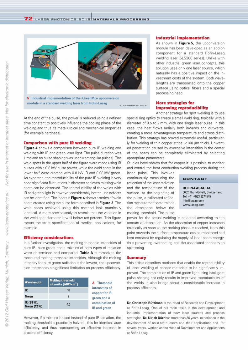
At the end of the pulse, the power is reduced using a defined
time constant to positively influence the cooling phase of the
welding and thus its metallurgical and mechanical properties
(for example hardness).
Comparison with pure IR welding
Figure 4 shows a comparison between pure IR welding and
welding with IR and green laser light. The pulse duration was
1 ms and no pulse shaping was used (rectangular pulses). The
weld spots in the upper half of the figure were made using IR
pulses with a 0.8 kW pulse power, while the weld spots in the
lower half were created with 0.8 kW IR and 0.08 kW green.
As expected, the reproducibility of the pure IR welding is very
poor, significant fluctuations in diameter and even missing weld
spots can be observed. The reproducibility of the welds with
IR and green light is however considerably better – no defects
can be identified. The insert in Figure 4 shows a series of weld
spots created using the pulse form described in Figure 3. The
weld spots achieved using this method look practically
identical. A more precise analysis reveals that the variation in
the weld spot diameter is well below ten percent. This figure
meets the strict specifications of medical applications, for
example.
Efficiency considerations
In a further investigation, the melting threshold intensities of
pure IR, pure green and a mixture of both types of radiation
were determined and compared. Table A summarizes the
measured melting threshold intensities. Although the melting
intensity for pure green radiation is the lowest, the upconver-
sion represents a significant limitation on process efficiency.
However, if a mixture is used instead of pure IR radiation, the
melting threshold is practically halved – this for identical laser
efficiency, and thus representing an effective increase in
process efficiency.
Industrial implementation
As shown in Figure 5, the upconversion
module has been developed as an add-on
component for a standard Rofin-Lasag
welding laser (SLS200 series). Unlike with
other industrial green laser concepts, this
solution uses only one laser source, which
naturally has a positive impact on the in-
vestment costs of the system. Both wave-
lengths are transported onto the copper
surface using optical fibers and a special
processing head.
More strategies for
improving reproducibility
Another strategy for spot welding is to use
special ring optics to create a small weld ring, typically with a
diameter of 0.5 to 2 mm, with one single laser pulse. In this
case, the heat flows radially both inwards and outwards,
creating a more advantageous temperature and stress distri-
bution. This strategy has proved extremely useful, particular-
ly for welding of thin copper strips (<100 µm thick). Unwant-
ed penetration caused by excessive intensities in the center
of the beam can be completely eliminated by selecting
appropriate parameters.
Studies have shown that for copper it is possible to monitor
and control the heat conduction welding process during the
laser pulse. This involves
continuously measuring the
reflection of the laser radiation
and the temperature of the
surface. At the beginning of
the pulse, a calibrated reflec-
tion measurement determines
the absorption below the
melting threshold. The pulse
power for the actual welding is selected according to the
amount of absorption. As the absorption of copper increases
erratically as soon as the melting phase is reached, from this
point onwards the surface temperature can be monitored and
kept constant by regulating the supply of laser beam energy,
thus preventing overheating and the associated tendency to
splattering
Summary
This article describes methods that enable the reproducibility
of laser welding of copper materials to be significantly im-
proved. The combination of IR and green light using intelligent
pulse shaping not only results in improved reproducibility of
the welds, it also brings about a considerable increase in
process efficiency.
Dr. Christoph Rüttiman is the Head of Research and Development
at Rofin-Lasag. One of his main tasks is the development and
industrial implementation of new laser sources and process
strategies. Dr. Ulrich Dürr has more than 30 years’ experience in the
development of solid-state lasers and their applications and, for
several years, worked as the Head of Development and Applications
at Rofin-Lasag.
72 l LASER+PHOTONICS 2 0 12 lMATERIALS PROCESSING
5 Industrial implementation of the ›GreenMix‹ upconversion module in a standard welding laser from Rofin-Lasag
© LASER+PHOTONICS
ROFIN-LASAG AG 3602 Thun-Gwatt, Switzerland
Tel. +41 (0)33 2274545
www.lasag.com
CONTACT
Wavelength Melting threshold intensity [MW/cm2]
IR 10
Green 2
IR (88 %), Green (12 %) 4.6
A Thresholdintensities ofcopper for IR,green and acombination of IR and green
70-72_LPX110018_rofinlasag_LPex2012 ax 15.12.2011 17:07 Uhr Seite 72
© 2
012
Car
l Han
ser V
erla
g, M
unic
h, G
erm
any
w
ww
.lase
r-ph
oton
ics.
eu
Not
for u
se in
inte
rnet
or i
ntra
net s
ites.
Not
for e
lect
roni
c di
strib
utio
n.
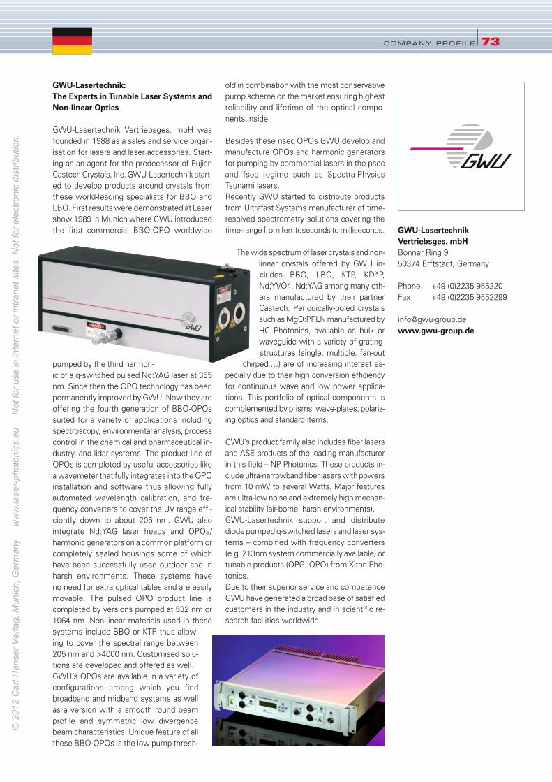
COMPANY PROF ILE l73
GWU-LasertechnikVertriebsges. mbH Bonner Ring 9
50374 Erftstadt, Germany
Phone +49 (0)2235 955220
Fax +49 (0)2235 9552299
www.gwu-group.de
GWU-Lasertechnik:The Experts in Tunable Laser Systems andNon-linear Optics
GWU-Lasertechnik Vertriebsges. mbH was
founded in 1988 as a sales and service organ-
isation for lasers and laser accessories. Start-
ing as an agent for the predecessor of Fujian
Castech Crystals, Inc. GWU-Lasertechnik start-
ed to develop products around crystals from
these world-leading specialists for BBO and
LBO. First results were demonstrated at Laser
show 1989 in Munich where GWU introduced
the first commercial BBO-OPO worldwide
pumped by the third harmon-
ic of a q-switched pulsed Nd:YAG laser at 355
nm. Since then the OPO technology has been
permanently improved by GWU. Now they are
offering the fourth generation of BBO-OPOs
suited for a variety of applications including
spectroscopy, environmental analysis, process
control in the chemical and pharmaceutical in-
dustry, and lidar systems. The product line of
OPOs is completed by useful accessories like
a wavemeter that fully integrates into the OPO
installation and software thus allowing fully
automated wavelength calibration, and fre-
quency converters to cover the UV range effi-
ciently down to about 205 nm. GWU also
integrate Nd:YAG laser heads and OPOs/
harmonic generators on a common platform or
completely sealed housings some of which
have been successfully used outdoor and in
harsh environments. These systems have
no need for extra optical tables and are easily
movable. The pulsed OPO product line is
completed by versions pumped at 532 nm or
1064 nm. Non-linear materials used in these
systems include BBO or KTP thus allow-
ing to cover the spectral range between
205 nm and >4000 nm. Customised solu-
tions are developed and offered as well.
GWU’s OPOs are available in a variety of
configurations among which you find
broadband and midband systems as well
as a version with a smooth round beam
profile and symmetric low divergence
beam characteristics. Unique feature of all
these BBO-OPOs is the low pump thresh-
old in combination with the most conservative
pump scheme on the market ensuring highest
reliability and lifetime of the optical compo-
nents inside.
Besides these nsec OPOs GWU develop and
manufacture OPOs and harmonic generators
for pumping by commercial lasers in the psec
and fsec regime such as Spectra-Physics
Tsunami lasers.
Recently GWU started to distribute products
from Ultrafast Systems manufacturer of time-
resolved spectrometry solutions covering the
time-range from femtoseconds to milliseconds.
The wide spectrum of laser crystals and non-
linear crystals offered by GWU in-
cludes BBO, LBO, KTP, KD*P,
Nd:YVO4, Nd:YAG among many oth-
ers manufactured by their partner
Castech. Periodically-poled crystals
such as MgO:PPLN manufactured by
HC Photonics, available as bulk or
waveguide with a variety of grating-
structures (single, multiple, fan-out
chirped,…) are of increasing interest es-
pecially due to their high conversion efficiency
for continuous wave and low power applica-
tions. This portfolio of optical components is
complemented by prisms, wave-plates, polariz-
ing optics and standard items.
GWU’s product family also includes fiber lasers
and ASE products of the leading manufacturer
in this field – NP Photonics. These products in-
clude ultra-narrowband fiber lasers with powers
from 10 mW to several Watts. Major features
are ultra-low noise and extremely high mechan-
ical stability (air-borne, harsh environments).
GWU-Lasertechnik support and distribute
diode pumped q-switched lasers and laser sys-
tems – combined with frequency converters
(e.g. 213nm system commercially available) or
tunable products (OPG, OPO) from Xiton Pho-
tonics.
Due to their superior service and competence
GWU have generated a broad base of satisfied
customers in the industry and in scientific re-
search facilities worldwide.
_FP_LPex2012 14.12.2011 16:05 Uhr Seite 73
© 2
012
Car
l Han
ser V
erla
g, M
unic
h, G
erm
any
w
ww
.lase
r-ph
oton
ics.
eu
Not
for u
se in
inte
rnet
or i
ntra
net s
ites.
Not
for e
lect
roni
c di
strib
utio
n.

PI miCos GmbHFreiburger Str. 30
79427 Eschbach
Tel. +49 (0)7634 5057-0
Fax +49 (0)7634 5057-99
www.pimicos.com
74 lCOMPANY PROF ILE
COMPANY PROF ILE
The new force in the worldof high-precision position-ing technologymiCos GmbH was founded in
Eschbach near Freiburg, Ger-
many in 1990. As PI miCos, it
now belongs to the company
group of PI (Physik Instru-
mente), located in Karlsruhe, Germany. With
currently more than 50 employees, the Breis-
gau company develops, produces and markets
innovative systems and components for high-
precision positioning applications throughout
the world. A main focus is on optical measure-
ment technology in research
and industry. For this purpose,
PI miCos offers customized
system solutions with mul-
tiple axes in addition to a
comprehensive standard pro-
gram. Wide-ranging applica-
tion know-how guarantees
the implementation of technically demanding
solutions. Flexible positioning systems for
ultra-high vacuum applications with parallel-
kinematics and six degrees of freedom are an
example of this, as are systems with linear
motors and air cushion bearings.
NUMERIK JENA GmbHIlmstraße 4
07743 Jena
Germany
Phone: +49 (0)3641 472888
Fax: +49 (0)3641 472820
www.numerikjena.de
The companyNUMERIK JENA draws from over 30 years of
experience in the development, manufacture
and sale of position encoders. The roots of pro-
duction metrology and its associated technol-
ogy for the manufacture of precision scales go
back to Carl Zeiss and Ernst Abbe.
In following this great tradition, the goal of all
our activities is continuous innovation and the
improvement of our products.
We orient ourselves to the demands of the in-
ternational market to which we can react flex-
ibly thanks to the modular character of our en-
coders.
The productsNUMERIK JENA offers po-
sitioning sensors with a
wide variety of options ac-
cording to the demands of
the application.
• high resolution for the pre-
cise dynamics of the actu-
ator
• high accuracy for accurate
and repeatable positioning
• low short-range errors for constant and
smooth motion
• low profile requirement for ease of imple-
mentation and to allow simple integration
with existing mechanics
• low mass for high acceleration
• high traversing speed for fast positioning and
high productivity
• customer friendly mounting tolerances for
low assembling costs
• high insensitivity against contamination for
high reliability
Applications• suppliers and users of lin-
ear and rotary actuators
• production equipment of
semiconducter industry
• linear, rotary and planar di-
rect drives
• torque motors
• coordinate measuring
equipment
• medical technology
_FP_LPex2012 14.12.2011 16:05 Uhr Seite 74
© 2
012
Car
l Han
ser V
erla
g, M
unic
h, G
erm
any
w
ww
.lase
r-ph
oton
ics.
eu
Not
for u
se in
inte
rnet
or i
ntra
net s
ites.
Not
for e
lect
roni
c di
strib
utio
n.
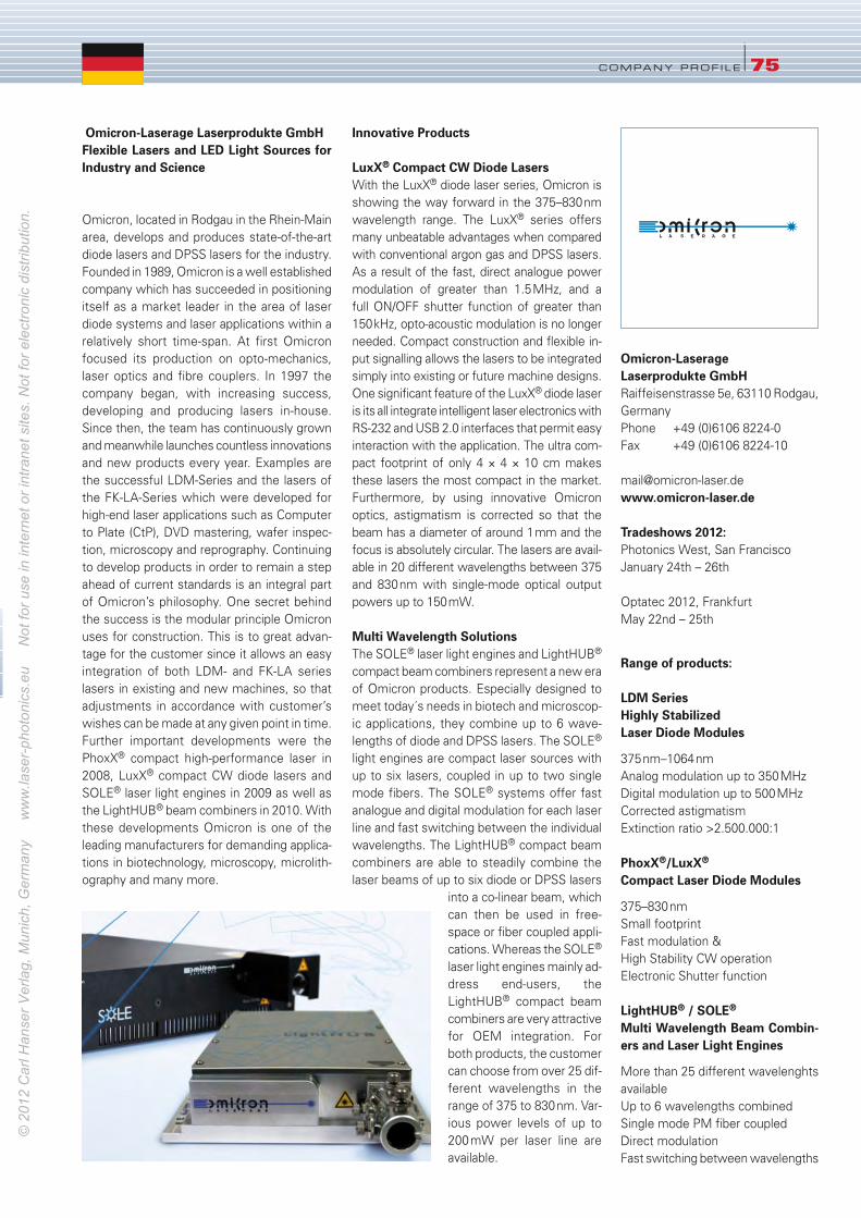
COMPANY PROF ILE l75
Omicron-Laserage Laserprodukte GmbHRaiffeisenstrasse 5e, 63110 Rodgau,
Germany
Phone +49 (0)6106 8224-0
Fax +49 (0)6106 8224-10
www.omicron-laser.de
Tradeshows 2012:Photonics West, San Francisco
January 24th – 26th
Optatec 2012, Frankfurt
May 22nd – 25th
Range of products:
LDM Series Highly Stabilized Laser Diode Modules
375nm–1064nm
Analog modulation up to 350MHz
Digital modulation up to 500MHz
Corrected astigmatism
Extinction ratio >2.500.000:1
PhoxX®/LuxX®
Compact Laser Diode Modules
375–830nm
Small footprint
Fast modulation &
High Stability CW operation
Electronic Shutter function
LightHUB® / SOLE®
Multi Wavelength Beam Combin-ers and Laser Light Engines
More than 25 different wavelenghts
available
Up to 6 wavelengths combined
Single mode PM fiber coupled
Direct modulation
Fast switching between wavelengths
Omicron-Laserage Laserprodukte GmbHFlexible Lasers and LED Light Sources forIndustry and Science
Omicron, located in Rodgau in the Rhein-Main
area, develops and produces state-of-the-art
diode lasers and DPSS lasers for the industry.
Founded in 1989, Omicron is a well established
company which has succeeded in positioning
itself as a market leader in the area of laser
diode systems and laser applications within a
relatively short time-span. At first Omicron
focused its production on opto-mechanics,
laser optics and fibre couplers. In 1997 the
company began, with increasing success,
developing and producing lasers in-house.
Since then, the team has continuously grown
and meanwhile launches countless innovations
and new products every year. Examples are
the successful LDM-Series and the lasers of
the FK-LA-Series which were developed for
high-end laser applications such as Computer
to Plate (CtP), DVD mastering, wafer inspec-
tion, microscopy and reprography. Continuing
to develop products in order to remain a step
ahead of current standards is an integral part
of Omicron’s philosophy. One secret behind
the success is the modular principle Omicron
uses for construction. This is to great advan-
tage for the customer since it allows an easy
integration of both LDM- and FK-LA series
lasers in existing and new machines, so that
adjustments in accordance with customer’s
wishes can be made at any given point in time.
Further important developments were the
PhoxX® compact high-performance laser in
2008, LuxX® compact CW diode lasers and
SOLE® laser light engines in 2009 as well as
the LightHUB® beam combiners in 2010. With
these developments Omicron is one of the
leading manufacturers for demanding applica-
tions in biotechnology, microscopy, microlith-
ography and many more.
Innovative Products
LuxX® Compact CW Diode LasersWith the LuxX® diode laser series, Omicron is
showing the way forward in the 375–830nm
wavelength range. The LuxX® series offers
many unbeatable advantages when compared
with conventional argon gas and DPSS lasers.
As a result of the fast, direct analogue power
modulation of greater than 1.5MHz, and a
full ON/OFF shutter function of greater than
150kHz, opto-acoustic modulation is no longer
needed. Compact construction and flexible in-
put signalling allows the lasers to be integrated
simply into existing or future machine designs.
One significant feature of the LuxX® diode laser
is its all integrate intelligent laser electronics with
RS-232 and USB 2.0 interfaces that permit easy
interaction with the application. The ultra com-
pact footprint of only 4 × 4 × 10 cm makes
these lasers the most compact in the market.
Furthermore, by using innovative Omicron
optics, astigmatism is corrected so that the
beam has a diameter of around 1mm and the
focus is absolutely circular. The lasers are avail-
able in 20 different wavelengths between 375
and 830nm with single-mode optical output
powers up to 150mW.
Multi Wavelength SolutionsThe SOLE® laser light engines and LightHUB®
compact beam combiners represent a new era
of Omicron products. Especially designed to
meet today´s needs in biotech and microscop-
ic applications, they combine up to 6 wave-
lengths of diode and DPSS lasers. The SOLE®
light engines are compact laser sources with
up to six lasers, coupled in up to two single
mode fibers. The SOLE® systems offer fast
analogue and digital modulation for each laser
line and fast switching between the individual
wavelengths. The LightHUB® compact beam
combiners are able to steadily combine the
laser beams of up to six diode or DPSS lasers
into a co-linear beam, which
can then be used in free-
space or fiber coupled appli-
cations. Whereas the SOLE®
laser light engines mainly ad-
dress end-users, the
LightHUB® compact beam
combiners are very attractive
for OEM integration. For
both products, the customer
can choose from over 25 dif-
ferent wavelengths in the
range of 375 to 830nm. Var-
ious power levels of up to
200mW per laser line are
available.
_FP_LPex2012 14.12.2011 16:05 Uhr Seite 75
© 2
012
Car
l Han
ser V
erla
g, M
unic
h, G
erm
any
w
ww
.lase
r-ph
oton
ics.
eu
Not
for u
se in
inte
rnet
or i
ntra
net s
ites.
Not
for e
lect
roni
c di
strib
utio
n.
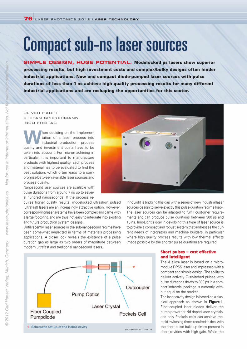
OL IVER HAUPT
STEFAN SP IEKERMANN
INGO FRE ITAG
When deciding on the implemen-
tation of a laser process into
industrial production, process
quality and investment costs have to be
taken into account. For micromachining in
particular, it is important to manufacture
products with highest quality. Each process
and material has to be evaluated to find the
best solution, which often leads to a com-
promise between available laser sources and
process quality.
Nanosecond laser sources are available with
pulse durations from around 7 ns up to sever-
al hundred nanoseconds. If the process re-
quires higher quality results, modelocked ultrashort pulsed
(ultrafast) lasers are an increasingly attractive option. However,
corresponding laser systems have been complex and came with
a large footprint, and are thus not easy to integrate into existing
and future production system designs.
Until recently, laser sources in the sub-nanosecond regime have
been somewhat neglected in terms of materials processing
applications. A closer look reveals the existence of a pulse
duration gap as large as two orders of magnitude between
modern ultrafast and traditional nanosecond lasers.
InnoLight is bridging this gap with a series of new industrial laser
sources design to serve exactly this pulse duration regime (gap).
The laser sources can be adapted to fulfill customer require-
ments and can produce pulse durations between 300 ps and
10 ns. InnoLight’s goal in devolping this type of laser source is
to provide a compact and robust system that addresses the cur-
rent needs of integrators and machine builders, in particular
where high quality process results with low thermal effects
(made possible by the shorter pulse duration) are required.
Short pulses – cost effective
and intelligent
The ›Helios‹ laser is based on a micro-
module DPSS laser and impresses with a
compact and simple design. The ability to
deliver actively Q-switched pulses with
pulse durations down to 300 ps in a com-
pact industrial package is currently with-
out equal on the market.
The laser cavity design is based on a clas-
sical approach as shown in Figure 1.
Fiber-coupled laser diodes deliver the
pump power for Nd-doped laser crystals,
and only Pockels cells can achieve the
rapid switching times required to deal with
the short pulse build-up times present in
short cavities with high gain. While the
76 l LASER+PHOTONICS 2 0 12 l LASER TECHNOLOGY
Compact sub-ns laser sourcesSIMPLE DESIGN, HUGE POTENTIAL. Modelocked ps lasers show superior
processing results, but high investment costs and complex/bulky designs often hinder
industrial applications. New and compact diode-pumped laser sources with pulse
durations of less than 1 ns achieve high quality processing results for many different
industrial applications and are reshaping the opportunities for this sector.
1 Schematic set-up of the Helios cavity © LASER+PHOTONICS
76-77_LPX110133_innolight_LPex2012 ax 15.12.2011 17:10 Uhr Seite 76
© 2
012
Car
l Han
ser V
erla
g, M
unic
h, G
erm
any
w
ww
.lase
r-ph
oton
ics.
eu
Not
for u
se in
inte
rnet
or i
ntra
net s
ites.
Not
for e
lect
roni
c di
strib
utio
n.
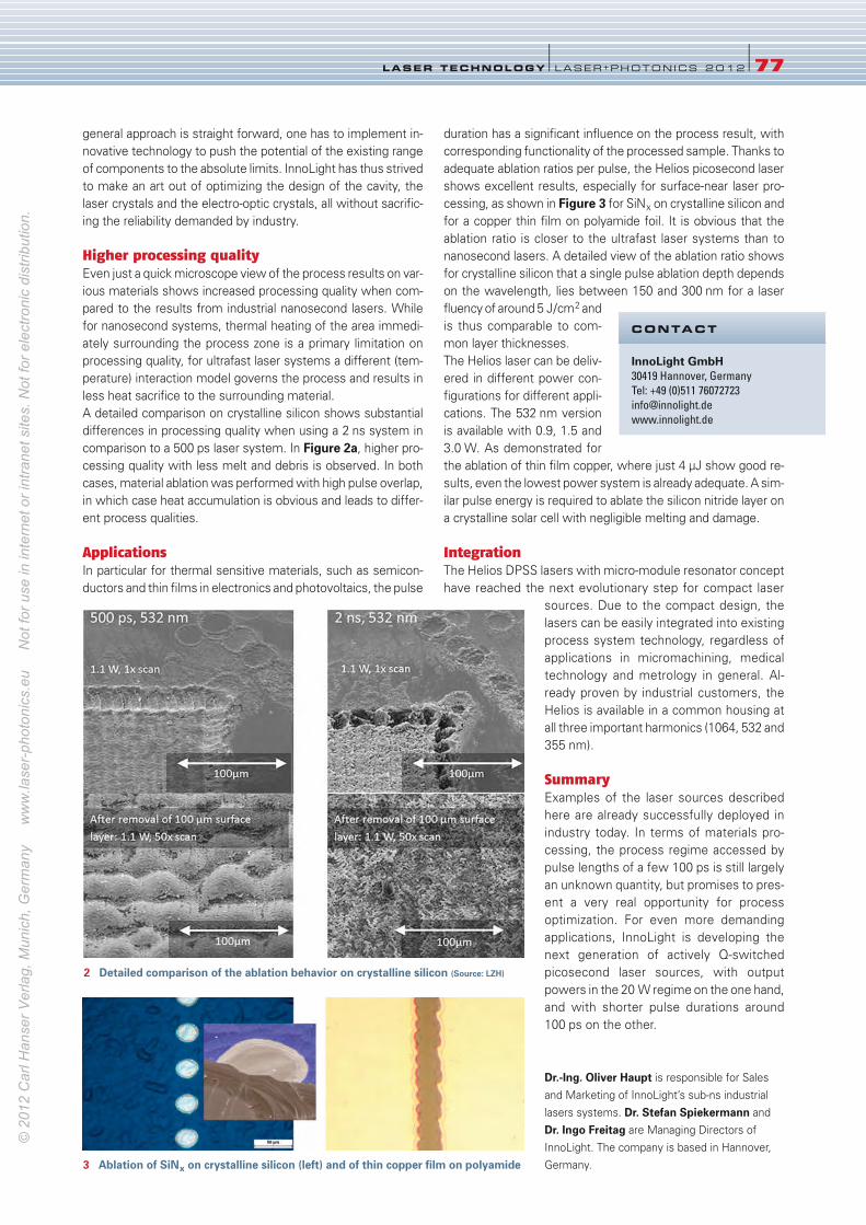
general approach is straight forward, one has to implement in-
novative technology to push the potential of the existing range
of components to the absolute limits. InnoLight has thus strived
to make an art out of optimizing the design of the cavity, the
laser crystals and the electro-optic crystals, all without sacrific-
ing the reliability demanded by industry.
Higher processing quality
Even just a quick microscope view of the process results on var-
ious materials shows increased processing quality when com-
pared to the results from industrial nanosecond lasers. While
for nanosecond systems, thermal heating of the area immedi-
ately surrounding the process zone is a primary limitation on
processing quality, for ultrafast laser systems a different (tem-
perature) interaction model governs the process and results in
less heat sacrifice to the surrounding material.
A detailed comparison on crystalline silicon shows substantial
differences in processing quality when using a 2 ns system in
comparison to a 500 ps laser system. In Figure 2a, higher pro-
cessing quality with less melt and debris is observed. In both
cases, material ablation was performed with high pulse overlap,
in which case heat accumulation is obvious and leads to differ-
ent process qualities.
Applications
In particular for thermal sensitive materials, such as semicon-
ductors and thin films in electronics and photovoltaics, the pulse
duration has a significant influence on the process result, with
corresponding functionality of the processed sample. Thanks to
adequate ablation ratios per pulse, the Helios picosecond laser
shows excellent results, especially for surface-near laser pro-
cessing, as shown in Figure 3 for SiNx on crystalline silicon and
for a copper thin film on polyamide foil. It is obvious that the
ablation ratio is closer to the ultrafast laser systems than to
nanosecond lasers. A detailed view of the ablation ratio shows
for crystalline silicon that a single pulse ablation depth depends
on the wavelength, lies between 150 and 300 nm for a laser
fluency of around 5 J/cm2 and
is thus comparable to com-
mon layer thicknesses.
The Helios laser can be deliv-
ered in different power con-
figurations for different appli-
cations. The 532 nm version
is available with 0.9, 1.5 and
3.0 W. As demonstrated for
the ablation of thin film copper, where just 4 µJ show good re-
sults, even the lowest power system is already adequate. A sim-
ilar pulse energy is required to ablate the silicon nitride layer on
a crystalline solar cell with negligible melting and damage.
Integration
The Helios DPSS lasers with micro-module resonator concept
have reached the next evolutionary step for compact laser
sources. Due to the compact design, the
lasers can be easily integrated into existing
process system technology, regardless of
applications in micromachining, medical
technology and metrology in general. Al-
ready proven by industrial customers, the
Helios is available in a common housing at
all three important harmonics (1064, 532 and
355 nm).
Summary
Examples of the laser sources described
here are already successfully deployed in
industry today. In terms of materials pro-
cessing, the process regime accessed by
pulse lengths of a few 100 ps is still largely
an unknown quantity, but promises to pres-
ent a very real opportunity for process
optimization. For even more demanding
applications, InnoLight is developing the
next generation of actively Q-switched
picosecond laser sources, with output
powers in the 20 W regime on the one hand,
and with shorter pulse durations around
100 ps on the other.
Dr.-Ing. Oliver Haupt is responsible for Sales
and Marketing of InnoLight’s sub-ns industrial
lasers systems. Dr. Stefan Spiekermann and
Dr. Ingo Freitag are Managing Directors of
InnoLight. The company is based in Hannover,
Germany.
LASER TECHNOLOGY l LASER+PHOTONICS 2012 l77
InnoLight GmbH 30419 Hannover, Germany
Tel: +49 (0)511 76072723
www.innolight.de
CONTACT
2 Detailed comparison of the ablation behavior on crystalline silicon (Source: LZH)
3 Ablation of SiNx on crystalline silicon (left) and of thin copper film on polyamide
76-77_LPX110133_innolight_LPex2012 ax 15.12.2011 17:10 Uhr Seite 77
© 2
012
Car
l Han
ser V
erla
g, M
unic
h, G
erm
any
w
ww
.lase
r-ph
oton
ics.
eu
Not
for u
se in
inte
rnet
or i
ntra
net s
ites.
Not
for e
lect
roni
c di
strib
utio
n.
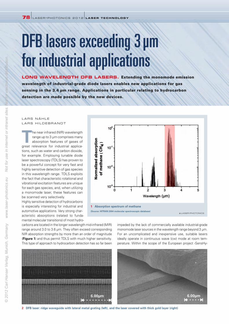
LARS NÄHLE
LARS H ILDEBRANDT
The near infrared (NIR) wavelength
range up to 3 µm comprises many
absorption features of gases of
great relevance for industrial applica-
tions, such as water and carbon dioxide,
for example. Employing tunable diode
laser spectroscopy (TDLS) has proven to
be a powerful concept for very fast and
highly sensitive detection of gas species
in this wavelength range. TDLS exploits
the fact that characteristic rotational and
vibrational excitation features are unique
for each gas species, and, when utilizing
a monomode laser, these features can
be scanned very selectively.
Highly sensitive detection of hydrocarbons
is especially interesting for industrial and
automotive applications. Very strong char-
acteristic absorptions (related to funda-
mental molecular transitions) of most hydro-
carbons are located in the longer wavelength mid-infrared (MIR)
range around 3.0 to 3.6 µm. They often exceed corresponding
NIR absorption strengths by more than an order of magnitude
(Figure 1) and thus permit TDLS with much higher sensitivity.
This type of approach to hydrocarbon detection has so far been
impeded by the lack of commercially available industrial-grade
monomode laser sources in the wavelength range beyond 3 µm.
For an uncomplicated and inexpensive use, suitable lasers
ideally operate in continuous wave (cw) mode at room tem-
perature. Within the scope of the European project ›SensHy‹
78 l LASER+PHOTONICS 2 0 12 l LASER TECHNOLOGY
DFB lasers exceeding 3 µm for industrial applications LONG WAVELENGTH DFB LASERS. Extending the monomode emission
wavelength of industrial-grade diode lasers enables new applications for gas
sensing in the 3.4 µm range. Applications in particular relating to hydrocarbon
detection are made possible by the new devices.
1 Absorption spectrum of methane (Source: HITRAN 2004 molecular spectroscopic database)
© LASER+PHOTONICS
2 DFB laser: ridge waveguide with lateral metal grating (left), and the laser covered with thick gold layer (right)
78-80_LPX110135_nanoplus_LPex2012 ax 15.12.2011 17:14 Uhr Seite 78
© 2
012
Car
l Han
ser V
erla
g, M
unic
h, G
erm
any
w
ww
.lase
r-ph
oton
ics.
eu
Not
for u
se in
inte
rnet
or i
ntra
net s
ites.
Not
for e
lect
roni
c di
strib
utio
n.
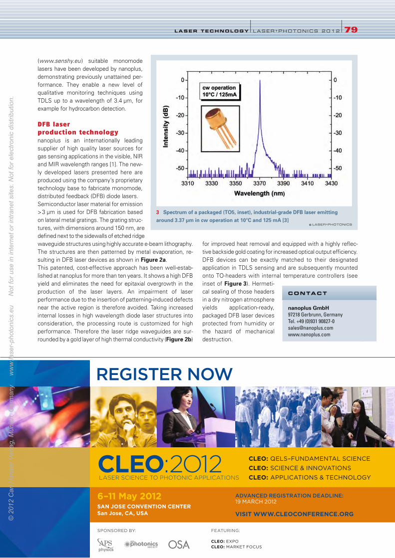
(www.senshy.eu) suitable monomode
lasers have been developed by nanoplus,
demonstrating previously unattained per-
formance. They enable a new level of
qualitative monitoring techniques using
TDLS up to a wavelength of 3.4 µm, for
example for hydrocarbon detection.
DFB laser
production technology
nanoplus is an internationally leading
supplier of high quality laser sources for
gas sensing applications in the visible, NIR
and MIR wavelength ranges [1]. The new-
ly developed lasers presented here are
produced using the company’s proprietary
technology base to fabricate monomode,
distributed feedback (DFB) diode lasers.
Semiconductor laser material for emission
>3 µm is used for DFB fabrication based
on lateral metal gratings. The grating struc-
tures, with dimensions around 150 nm, are
defined next to the sidewalls of etched ridge
waveguide structures using highly accurate e-beam lithography.
The structures are then patterned by metal evaporation, re-
sulting in DFB laser devices as shown in Figure 2a.
This patented, cost-effective approach has been well-estab-
lished at nanoplus for more than ten years. It shows a high DFB
yield and eliminates the need for epitaxial overgrowth in the
production of the laser layers. An impairment of laser
performance due to the insertion of patterning-induced defects
near the active region is therefore avoided. Taking increased
internal losses in high wavelength diode laser structures into
consideration, the processing route is customized for high
performance. Therefore the laser ridge waveguides are sur-
rounded by a gold layer of high thermal conductivity (Figure 2b)
for improved heat removal and equipped with a highly reflec-
tive backside gold coating for increased optical output efficiency.
DFB devices can be exactly matched to their designated
application in TDLS sensing and are subsequently mounted
onto TO-headers with internal temperature controllers (see
inset of Figure 3). Hermeti-
cal sealing of those headers
in a dry nitrogen atmosphere
yields application-ready,
packaged DFB laser devices
protected from humidity or
the hazard of mechanical
destruction.
LASER TECHNOLOGY l LASER+PHOTONICS 2012 l79
3 Spectrum of a packaged (TO5, inset), industrial-grade DFB laser emittingaround 3.37 µm in cw operation at 10°C and 125 mA [3]
© LASER+PHOTONICS
REGISTER NOW
SPONSORED BY: FEATURING:
CLEO: EXPOCLEO: MARKET FOCUS
6–11 May 2012SAN JOSE CONVENTION CENTERSan Jose, CA, USA
CLEO: QELS–FUNDAMENTAL SCIENCE
CLEO: SCIENCE & INNOVATIONS
CLEO: APPLICATIONS & TECHNOLOGYCLEO:2O12 LASER SCIENCE TO PHOTONIC APPLICATIONS
VISIT WWW.CLEOCONFERENCE.ORG
ADVANCED REGISTRATION DEADLINE: 19 MARCH 2012
nanoplus GmbH 97218 Gerbrunn, Germany
Tel. +49 (0)931 90827-0
www.nanoplus.com
CONTACT
78-80_LPX110135_nanoplus_LPex2012 ax 15.12.2011 17:14 Uhr Seite 79
© 2
012
Car
l Han
ser V
erla
g, M
unic
h, G
erm
any
w
ww
.lase
r-ph
oton
ics.
eu
Not
for u
se in
inte
rnet
or i
ntra
net s
ites.
Not
for e
lect
roni
c di
strib
utio
n.
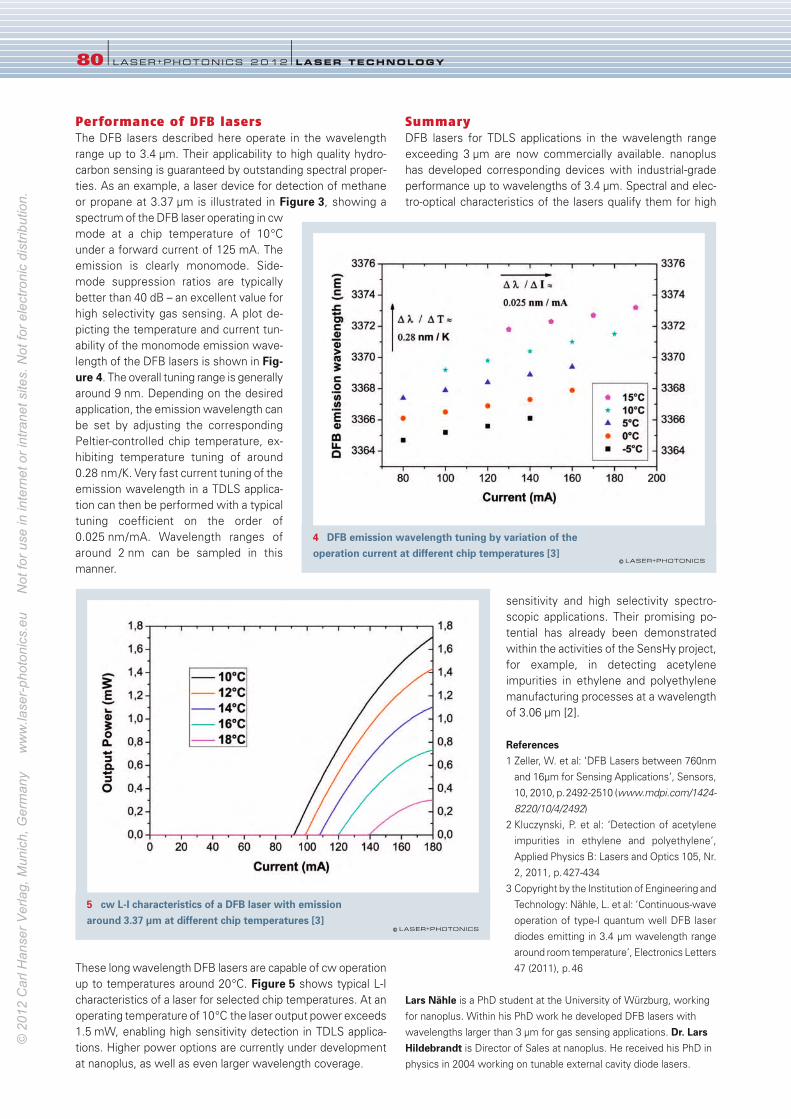
Performance of DFB lasers
The DFB lasers described here operate in the wavelength
range up to 3.4 µm. Their applicability to high quality hydro-
carbon sensing is guaranteed by outstanding spectral proper-
ties. As an example, a laser device for detection of methane
or propane at 3.37 µm is illustrated in Figure 3, showing a
spectrum of the DFB laser operating in cw
mode at a chip temperature of 10°C
under a forward current of 125 mA. The
emission is clearly monomode. Side-
mode suppression ratios are typically
better than 40 dB – an excellent value for
high selectivity gas sensing. A plot de-
picting the temperature and current tun-
ability of the monomode emission wave-
length of the DFB lasers is shown in Fig-ure 4. The overall tuning range is generally
around 9 nm. Depending on the desired
application, the emission wavelength can
be set by adjusting the corresponding
Peltier-controlled chip temperature, ex-
hibiting temperature tuning of around
0.28 nm/K. Very fast current tuning of the
emission wavelength in a TDLS applica-
tion can then be performed with a typical
tuning coefficient on the order of
0.025 nm/mA. Wavelength ranges of
around 2 nm can be sampled in this
manner.
These long wavelength DFB lasers are capable of cw operation
up to temperatures around 20°C. Figure 5 shows typical L-I
characteristics of a laser for selected chip temperatures. At an
operating temperature of 10°C the laser output power exceeds
1.5 mW, enabling high sensitivity detection in TDLS applica-
tions. Higher power options are currently under development
at nanoplus, as well as even larger wavelength coverage.
Summary
DFB lasers for TDLS applications in the wavelength range
exceeding 3 µm are now commercially available. nanoplus
has developed corresponding devices with industrial-grade
performance up to wavelengths of 3.4 µm. Spectral and elec-
tro-optical characteristics of the lasers qualify them for high
sensitivity and high selectivity spectro-
scopic applications. Their promising po-
tential has already been demonstrated
within the activities of the SensHy project,
for example, in detecting acetylene
impurities in ethylene and polyethylene
manufacturing processes at a wavelength
of 3.06 µm [2].
References1 Zeller, W. et al: ‘DFB Lasers between 760nm
and 16µm for Sensing Applications’, Sensors,
10, 2010, p.2492-2510 (www.mdpi.com/1424-
8220/10/4/2492)
2 Kluczynski, P. et al: ‘Detection of acetylene
impurities in ethylene and polyethylene’,
Applied Physics B: Lasers and Optics 105, Nr.
2, 2011, p.427-434
3 Copyright by the Institution of Engineering and
Technology: Nähle, L. et al: ‘Continuous-wave
operation of type-I quantum well DFB laser
diodes emitting in 3.4 µm wavelength range
around room temperature’, Electronics Letters
47 (2011), p.46
Lars Nähle is a PhD student at the University of Würzburg, working
for nanoplus. Within his PhD work he developed DFB lasers with
wavelengths larger than 3 µm for gas sensing applications. Dr. LarsHildebrandt is Director of Sales at nanoplus. He received his PhD in
physics in 2004 working on tunable external cavity diode lasers.
80 l LASER+PHOTONICS 2 0 12 l LASER TECHNOLOGY
5 cw L-I characteristics of a DFB laser with emission around 3.37 µm at different chip temperatures [3]
© LASER+PHOTONICS
4 DFB emission wavelength tuning by variation of the operation current at different chip temperatures [3]
© LASER+PHOTONICS
78-80_LPX110135_nanoplus_LPex2012 ax 15.12.2011 17:14 Uhr Seite 80
© 2
012
Car
l Han
ser V
erla
g, M
unic
h, G
erm
any
w
ww
.lase
r-ph
oton
ics.
eu
Not
for u
se in
inte
rnet
or i
ntra
net s
ites.
Not
for e
lect
roni
c di
strib
utio
n.

APE – Angewandte Physik & Elektronik GmbH
is a premier manufacturer of non-linear instru-
ments for the generation of ultrafast laser puls-
es with widely tuneable wavelengths as well
as their measurement and management.
APE was founded in 1992 in Berlin, Germany.
APE´s high-tech devices can be found in almost
all renowned institutes and universities, the
main field of operation being basic research in
physics, chemistry, biology and medical sci-
ence.
A team of experienced physicists, electronic
engineers, software experts and technical de-
signers develops user oriented instruments.
These instruments are manufactured in the
company’s own mechanical and optical pro-
duction facilities. A worldwide net of distribu-
tors guarantees easy access to local customer
and product support.
Our main product lines include Ultrafast Pulse
Diagnostics, Pulse Management, Wavelength
Conversion and Acousto-optics. As part of a
line of wavelength conversion we provide syn-
chronously pumped OPO and solutions of har-
monic generation. Technology leading pulse di-
agnostic devices are for instance highly flexi-
ble autocorrelators or diagnostics for phase
resolved measurements. Pulse Management
solutions such as pulse compressors, cavity
dumpers and pulse pickers are a well estab-
lished part of our product portfolio.
COMPANY PROF ILE l81
APE Angewandte Physik &Elektronik GmbHPlauener Strasse 163-165, Haus N
13053 Berlin, Germany
Phone +49 (0)30 98601130
Fax +49 (0)30 986011333
www.ape-berlin.com
SVS-VISTEK GmbH 82229 Seefeld/Germany, Tel. +49 - (0) 81 52 - 99 85 - 0, [email protected]
Scale Your Vision
Resolution: HR Series
Robust: CF Series
Mini: ECO Series
Flexibility: SLC Series
Speed: EVO Series
www.svs-vistek.com
_FP_LPex2012 15.12.2011 13:41 Uhr Seite 81
© 2
012
Car
l Han
ser V
erla
g, M
unic
h, G
erm
any
w
ww
.lase
r-ph
oton
ics.
eu
Not
for u
se in
inte
rnet
or i
ntra
net s
ites.
Not
for e
lect
roni
c di
strib
utio
n.
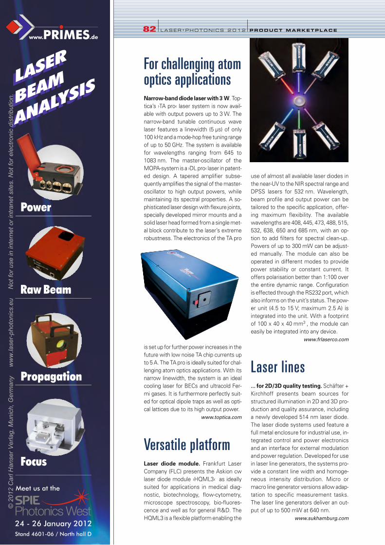
For challenging atomoptics applicationsNarrow-band diode laser with 3 W. Top-
tica’s ›TA pro‹ laser system is now avail-
able with output powers up to 3 W. The
narrow-band tunable continuous wave
laser features a linewidth (5 µs) of only
100 kHz and a mode-hop free tuning range
of up to 50 GHz. The system is available
for wavelengths ranging from 645 to
1083 nm. The master-oscillator of the
MOPA-system is a ›DL pro‹ laser in patent-
ed design. A tapered amplifier subse-
quently amplifies the signal of the master-
oscillator to high output powers, while
maintaining its spectral properties. A so-
phisticated laser design with flexure joints,
specially developed mirror mounts and a
solid laser head formed from a single met-
al block contribute to the laser’s extreme
robustness. The electronics of the TA pro
is set up for further power increases in the
future with low noise TA chip currents up
to 5 A. The TA pro is ideally suited for chal-
lenging atom optics applications. With its
narrow linewidth, the system is an ideal
cooling laser for BECs and ultracold Fer-
mi gases. It is furthermore perfectly suit-
ed for optical dipole traps as well as opti-
cal lattices due to its high output power.
www.toptica.com
Versatile platform Laser diode module. Frankfurt Laser
Company (FLC) presents the Askion cw
laser diode module ›HQML3‹ as ideally
suited for applications in medical diag-
nostic, biotechnology, flow-cytometry,
microscope spectroscopy, bio-fluores-
cence and well as for general R&D. The
HQML3 is a flexible platform enabling the
use of almost all available laser diodes in
the near-UV to the NIR spectral range and
DPSS lasers for 532 nm. Wavelength,
beam profile and output power can be
tailored to the specific application, offer-
ing maximum flexibility. The available
wavelengths are 408, 445, 473, 488, 515,
532, 638, 650 and 685 nm, with an op-
tion to add filters for spectral clean-up.
Powers of up to 300 mW can be adjust-
ed manually. The module can also be
operated in different modes to provide
power stability or constant current. It
offers polarisation better than 1:100 over
the entire dynamic range. Configuration
is effected through the RS232 port, which
also informs on the unit’s status. The pow-
er unit (4.5 to 15 V; maximum 2.5 A) is
integrated into the unit. With a footprint
of 100 x 40 x 40 mm3 , the module can
easily be integrated into any device.
www.frlaserco.com
Laser lines... for 2D/3D quality testing. Schäfter +
Kirchhoff presents beam sources for
structured illumination in 2D and 3D pro-
duction and quality assurance, including
a newly developed 514 nm laser diode.
The laser diode systems used feature a
full metal enclosure for industrial use, in-
tegrated control and power electronics
and an interface for external modulation
and power regulation. Developed for use
in laser line generators, the systems pro-
vide a constant line width and homoge-
neous intensity distribution. Micro or
macro line generator versions allow adap-
tation to specific measurement tasks.
The laser line generators deliver an out-
put of up to 500 mW at 640 nm.
www.sukhamburg.com
82 l LASER+PHOTONICS 2 0 12 lPRODUCT MARKETPLACE
82-83_produkte_LPex2012_x 15.12.2011 17:17 Uhr Seite 82
© 2
012
Car
l Han
ser V
erla
g, M
unic
h, G
erm
any
w
ww
.lase
r-ph
oton
ics.
eu
Not
for u
se in
inte
rnet
or i
ntra
net s
ites.
Not
for e
lect
roni
c di
strib
utio
n.
Near perfect beamBlue solid state disk laser. In coopera-
tion with partners Xiton Photonics and the
Institute for Medical Laser Technologies
of Ulm University, Germany, Z-Laser has
developed a blue 457 nm emitting laser
module with a beam quality of M2= 1.0
and an optical power of >500 mW.
Thanks to a new efficient pumping
concept for the solid state disk, the ›Z-
Blue beam‹ could be ›packaged‹ in a
compact housing. An 880 nm emitting
laser bar pumps the disk inside a newly
developed optical resonance system. The
module can be equipped with air cooling
or with water cooling. Due to its robust
construction and cost-effective cooling
system, the laser is suitable for use in
industrial environments as well as in the
medical sector.
www.z-laser.com
Homogenized and conduction-cooledLine source at 600 W, 880 nm. Dilas is
now delivering a new conduction-cooled,
multi-bar, line-source module with a homo-
geneous top hat optical beam profile in the
slow axis and diffraction limited profile
in the fast axis. This module is capable of
600 W power output at 880 nm ±5 nm. It
offers a 97.5 percent (±2.5 percent)
homogenized intensity profile in the slow
axis. The line dimensions are 10.5 mm x
325 µm (nominal). Customized focus
geometries can be offered as well. De-
signed for materials processing applica-
tions, these homogenized, multi-bar mod-
ules are ideal for solar, plastics welding,
semiconductor processing and thermal
annealing. They are available with option-
al features to include a power monitor and
user exchangeable protection window.
www.dilas.com
Opportune window Medical laser with replaceable win-dow. Limo Lissotschenko Mikrooptik
have fitted their compact L-Mount type
fiber-coupled diode laser modules with an
additional replaceable window. This helps
save time and money when fibers have
to be replaced, as is often the case in
medical applications. The laser in a com-
pact and hermetically sealed housing
outputs 30 to 60 W at 808 to 980 nm. The
beam is directed to its target by a fiber
connection with razor-thin fibers (dia-
meter: 200 and 400 µm) through a glass
window. In the newly designed housing,
an additional replaceable window is fitted
right behind the fiber connection. It pro-
tects the actual fixed window from the
effects of fiber destruction and can be
replaced quickly. www.limo.de
Suitable for MOPATapered amplifier. The GaAs-based ta-
pered amplifier TA-0915-1500 from m2k-
laser has an operating range of 905 to
925 nm and is suitable for MOPA (master
oscillator power amplifier) setups up to
1500 mW. Both rear and front facets have
an anti-reflection coating of less than
0.01 percent to avoid laser action of the
amplifier chip itself. The module offers a
beam propagation value M2<1.6 and a
sidemode suppression of more than
40 dB. Possible applications for MOPA
setups with tapered amplifiers are optical
cooling, optical traps or high resolution
absorption or Raman spectroscopy. The
device can be mounted on a C-mount or
optionally on a DHP inset or a DHP frame
for better handling. The module can be
ordered with selected beam quality para-
meters M2 and is also available for exter-
nal cavity configurations.
www.m2k-laser.de
PRODUCT MARKETPLACE l LASER+PHOTONICS 2012 l83
High Performance Optical Computing
Supports 64-bit and multi-core systemsDesign and optimize optical systems
500+ design examples, 8000+ catalogue lenses
Includes comprehensive Thin-Film PackageIllumination with real sourcesZoom and multiconfiguration
Polarization raytraceSequential and non-sequential models
Optenso, Optical Engineering Software, Kugelstr. 205, CH-9435 Heerbrugg, www.optenso.com
PSF
Source
3D-View
Fast Optical Design, Illumination, Thin Film Design using OpTaliX
82-83_produkte_LPex2012_x 15.12.2011 17:17 Uhr Seite 83
© 2
012
Car
l Han
ser V
erla
g, M
unic
h, G
erm
any
w
ww
.lase
r-ph
oton
ics.
eu
Not
for u
se in
inte
rnet
or i
ntra
net s
ites.
Not
for e
lect
roni
c di
strib
utio
n.
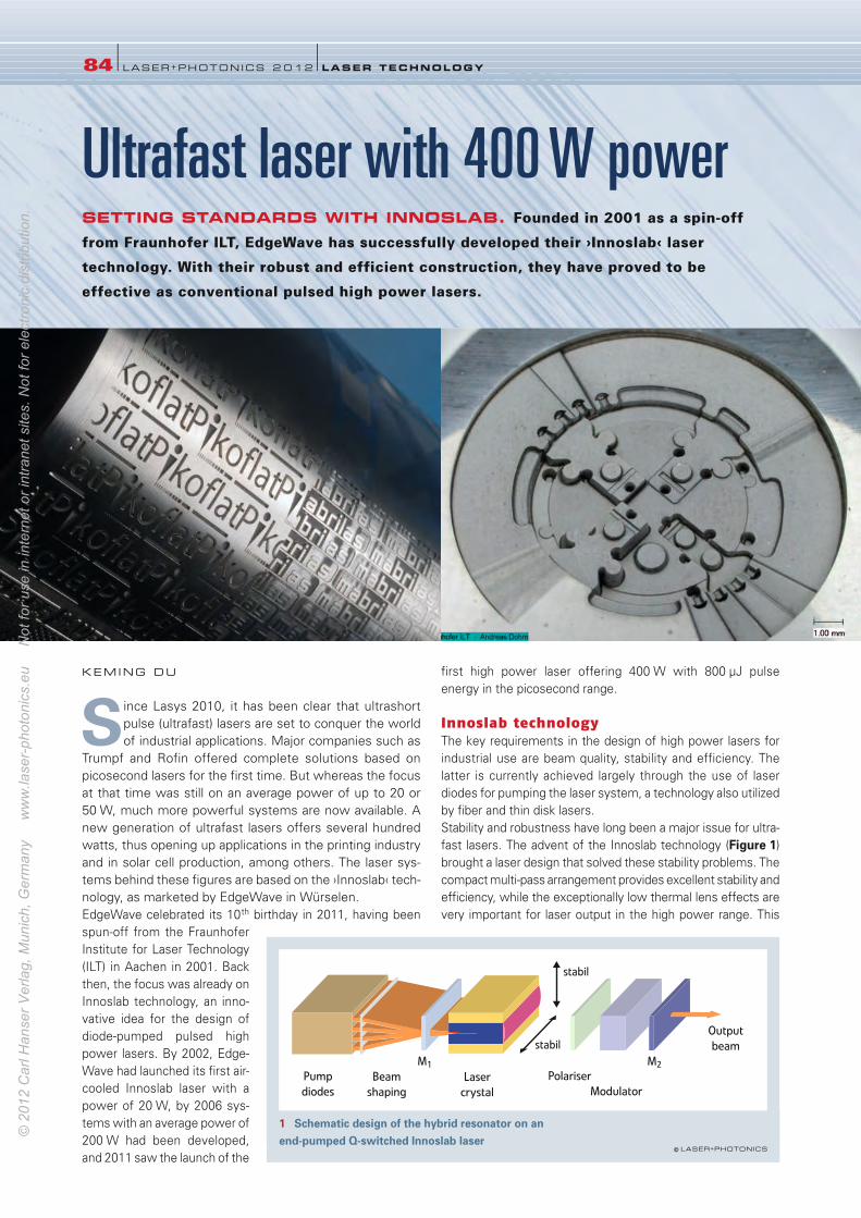
KEMING DU
Since Lasys 2010, it has been clear that ultrashort
pulse (ultrafast) lasers are set to conquer the world
of industrial applications. Major companies such as
Trumpf and Rofin offered complete solutions based on
picosecond lasers for the first time. But whereas the focus
at that time was still on an average power of up to 20 or
50 W, much more powerful systems are now available. A
new generation of ultrafast lasers offers several hundred
watts, thus opening up applications in the printing industry
and in solar cell production, among others. The laser sys-
tems behind these figures are based on the ›Innoslab‹ tech-
nology, as marketed by EdgeWave in Würselen.
EdgeWave celebrated its 10th birthday in 2011, having been
spun-off from the Fraunhofer
Institute for Laser Technology
(ILT) in Aachen in 2001. Back
then, the focus was already on
Innoslab technology, an inno-
vative idea for the design of
diode-pumped pulsed high
power lasers. By 2002, Edge-
Wave had launched its first air-
cooled Innoslab laser with a
power of 20 W, by 2006 sys-
tems with an average power of
200 W had been developed,
and 2011 saw the launch of the
first high power laser offering 400 W with 800 µJ pulse
energy in the picosecond range.
Innoslab technology
The key requirements in the design of high power lasers for
industrial use are beam quality, stability and efficiency. The
latter is currently achieved largely through the use of laser
diodes for pumping the laser system, a technology also utilized
by fiber and thin disk lasers.
Stability and robustness have long been a major issue for ultra-
fast lasers. The advent of the Innoslab technology (Figure 1)
brought a laser design that solved these stability problems. The
compact multi-pass arrangement provides excellent stability and
efficiency, while the exceptionally low thermal lens effects are
very important for laser output in the high power range. This
84 l LASER+PHOTONICS 2 0 12 l LASER TECHNOLOGY
Ultrafast laser with 400 W powerSETTING STANDARDS WITH INNOSLAB. Founded in 2001 as a spin-off
from Fraunhofer ILT, EdgeWave has successfully developed their ›Innoslab‹ laser
technology. With their robust and efficient construction, they have proved to be
effective as conventional pulsed high power lasers.
Pump-dioden
Strah-formung
Laser-kristall
M1 M2Polarisator
stabil
stabil
Modulator
Laserstrahl
1 Schematic design of the hybrid resonator on an end-pumped Q-switched Innoslab laser
© LASER+PHOTONICS
Pump diodes
Beamshaping
Laser crystal
Output beam
Polariser Modulator
84-85_LPX110125_edgewave_LPex2012 ax 15.12.2011 17:20 Uhr Seite 84
© 2
012
Car
l Han
ser V
erla
g, M
unic
h, G
erm
any
w
ww
.lase
r-ph
oton
ics.
eu
Not
for u
se in
inte
rnet
or i
ntra
net s
ites.
Not
for e
lect
roni
c di
strib
utio
n.

makes the Innoslab systems exceptionally
well suited for industrial applications in the
pulsed high power regime, delivering very
short pulses and excellent beam quality,
even at high average power. A further ad-
vantage is the flexibility of the system in
terms of the beam profile. Minor changes
to the design enable circles or rectangles
with a different intensity distribution to be
created (Figure 2).
The Innoslab concept allows complete laser
oscillators to be constructed that have
proven to be effective both for high powers
and in oscillator/amplifier configurations.
The new QX series reaches a specified
power of 400 W (Figure 3). A similar design
featuring two coupled-amplifier stages
achieved the current record of over 1 kW average power in an
ultrashort pulse laser developed at the Fraunhofer ILT [1].
Even though the technology has been developed for industrial
applications, the Innoslab technology still holds various gener-
al records for pulsed laser technology. As a result, the concept
earned the coveted ›Innovation Award Laser Technology 2010‹
(with the Q-switched Innoslab laser) at the AKL ’10 laser
congress.
Applications
Picosecond laser pulses allow so-called ›cold‹ ablation, which
means that there is little to no thermal influence on adjacent
areas. The material is evaporated so quickly that no heat af-
fected zone (HAZ) is produced. One application of high power
ultrafast lasers can be found in the manufacture of high-quali-
ty embossing cylinders for printing (title picture, left), where
processing of large areas with a high throughput is required,
while retaining maximum precision and a high aspect ratio. The
almost cold evaporation of materials using ultrafast lasers with
a high beam quality and several 10 µJ of pulse energy cuts away
a tiny but well defined slice with a diameter of 10 µm and a
depth of 100 nm per pulse. Combining these slices generates
the embossing structures on the outer sleeve of cylinder. Be-
cause of the tiny volume of the ablated slices, a level of high
lateral and depth resolution can be achieved that would be
impossible with a more thermal process.
Production-capable processing of embossing cylinders requires
high pulse repetition rates and high average powers. The lasers
from the new QX series deliver 400 W with 10 ps laser pulses
and a pulse repetition rate of up to 20 MHz, all in a very com-
pact housing. This qualifies them as OEM systems for micro-
processing with a high throughput and high precision.
Another application for Inno-
slab lasers can be found in
tool manufacture (title pic-ture, right). Here, recise
ablation without significant
deposits of melted material
is crucial. Compared to abla-
tion with conventional Q-
switched solid state lasers,
the lasers from the PX or QX series with ps pulse duration
evaporate the target with no melted material, at high precision
and free of recast. Point by point and layer by layer ablation
can thus be used to produce high precision tools.
Summary
Stable ultrafast lasers with the robust Innoslab design are
conquering the materials processing market. Systems from
EdgeWave with more than 400 W average power and up to 1 mJ
of pulse energy [3] are opening up a previously unattainable
power range and thus creating new applications or significant-
ly increasing the throughput in established processes.
References 1 Russbueldt, P. et al: ’Compact diode-pumped1.1 kW Yb:YAG Innoslab
femtosecond amplifier’; Opt. Lett. 35; Nr 24, S. 4169-4171, 2010
2 Du, K.: ‘Thin layer ablation with lasers of different beam profiles - En-
ergy efficiency and overfilling factor’; SPIE Proc. Vol. 7202, Laser-
based Micro- and Nanopackaging and Assembly III, Wilhelm Pfleg-
ing et al, Editors, 72020Q, 2009
3 Li, D., Du, K.: ‘Picosecond laser with 400 W average power and 1 mJ
pulse energy’; SPIE Proc. Vol. 7912, Solid State Lasers XX: Tech-
nology & Devices, W. Andrew Clarkson et al, Editors, 79120N, 2011
Dr. rer. nat. Keming Du is founder and Managing Director of EdgeWave.
LASER TECHNOLOGY l LASER+PHOTONICS 2012 l85
EdgeWave GmbH 52146 Würselen, Germany
Tel. +49 (0)2405 41860
www.edge-wave.com
CONTACT
2 The concept of the Innoslab laser allows various beam profiles to be created relatively easily
© LASER+PHOTONICS
Line shaped top-hat
Rectangular top-hat
Circular Gausssian Square top-hat
3 The new QX series of lasers with integrated amplifier delivery 400 W with 10 pspulses and a pulse repetition rate of up to 20 MHz, yet have a very compact design
84-85_LPX110125_edgewave_LPex2012 ax 15.12.2011 17:20 Uhr Seite 85
© 2
012
Car
l Han
ser V
erla
g, M
unic
h, G
erm
any
w
ww
.lase
r-ph
oton
ics.
eu
Not
for u
se in
inte
rnet
or i
ntra
net s
ites.
Not
for e
lect
roni
c di
strib
utio
n.
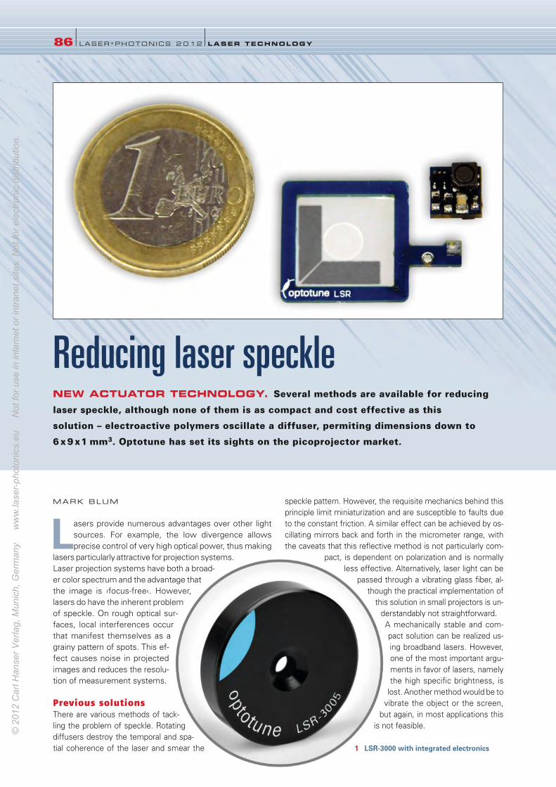
MARK BLUM
Lasers provide numerous advantages over other light
sources. For example, the low divergence allows
precise control of very high optical power, thus making
lasers particularly attractive for projection systems.
Laser projection systems have both a broad-
er color spectrum and the advantage that
the image is ›focus-free‹. However,
lasers do have the inherent problem
of speckle. On rough optical sur-
faces, local interferences occur
that manifest themselves as a
grainy pattern of spots. This ef-
fect causes noise in projected
images and reduces the resolu-
tion of measurement systems.
Previous solutions
There are various methods of tack-
ling the problem of speckle. Rotating
diffusers destroy the temporal and spa-
tial coherence of the laser and smear the
speckle pattern. However, the requisite mechanics behind this
principle limit miniaturization and are susceptible to faults due
to the constant friction. A similar effect can be achieved by os-
cillating mirrors back and forth in the micrometer range, with
the caveats that this reflective method is not particularly com-
pact, is dependent on polarization and is normally
less effective. Alternatively, laser light can be
passed through a vibrating glass fiber, al-
though the practical implementation of
this solution in small projectors is un-
derstandably not straightforward.
A mechanically stable and com-
pact solution can be realized us-
ing broadband lasers. However,
one of the most important argu-
ments in favor of lasers, namely
the high specific brightness, is
lost. Another method would be to
vibrate the object or the screen,
but again, in most applications this
is not feasible.
86 l LASER+PHOTONICS 2 0 12 l LASER TECHNOLOGY
Reducing laser speckleNEW ACTUATOR TECHNOLOGY. Several methods are available for reducing
laser speckle, although none of them is as compact and cost effective as this
solution – electroactive polymers oscillate a diffuser, permiting dimensions down to
6 x 9 x1 mm3. Optotune has set its sights on the picoprojector market.
1 LSR-3000 with integrated electronics
86-87_LPX110102_optotune_LPex2012 ax 15.12.2011 17:32 Uhr Seite 86
© 2
012
Car
l Han
ser V
erla
g, M
unic
h, G
erm
any
w
ww
.lase
r-ph
oton
ics.
eu
Not
for u
se in
inte
rnet
or i
ntra
net s
ites.
Not
for e
lect
roni
c di
strib
utio
n.

Electroactive polymers
The ›Laser Speckle Reducer‹ (LSR) (Figure 1) from Optotune
functions in a similar way to a rotating diffuser, but is many
times more compact and economical. The principle is simple –
a diffuser is mounted on an elastic membrane and moved back
and forth using electroactive polymers (Figure 2). With the
correct electrode geometry and appropriate actuation, planar
circular oscillation of the diffuser can be generated, with later-
al deflections of 100 to 500 µm at frequencies of 300 to 800 Hz,
depending on the size.
The secret behind the solution is actuators made of electroac-
tive polymers (EAPs, also known as artificial muscles). Flexible
electrically conductive surfaces are attached to the top and bot-
tom of a thin elastomer film. When a voltage is applied between
the two electrodes, these are charged according to the princi-
ble of a plate capacitor, attract one another and thus squeeze
the elastic film. Given that the volume remains constant, the
electrodes expand laterally, theoretically by up to 40 percent,
and thus move the diffuser.
Small, effective and economical
The major advantage of this technology is the extremely com-
pact design. While a generously proportioned design for a 10 mm
wide diffuser has a total size of 22x22x1 mm3, just 6x9x1 mm3
is possible for a diffuser size of 2x4 mm2, for example. Com-
pared to one-dimensional rotation, the two-dimensional circular
movement method is also more effective, as a larger area of the
diffuser surface can be utilized. Other advantages of the LSR are
directly attributable to the basic EAP technology – there are no
mechanics so it is completely silent, it has a long operating
life-time and it can be used over a wide temperature range. The
power consumption is also extremely low.
The maximum speckle reduction (Figure 3) that can be achieved
depends on the entire optical system. Significant reduction can
be expected at high frequencies and through the use of larger
oscillation amplitudes, high resolution diffuser patterns and long
observer integration times. As with all methods based on dif-
fusers, an increase in the divergence of the laser beam must
be tolerated, this increase being all the more significant with
very fine diffuser structures. The optical design may then need
to incorporate additional optics to collimate the laser.
The electronics requirements also need to be considered. Al-
though actuation of the LSR is simple and requires little power,
electrical voltages of up to 300 V are often necessary to achieve
the desired amplitude of oscillation. As a result, battery operat-
ed devices must include voltage conversion electronics, although
this only takes up around 40 mm2 of PCB space.
The breakthrough?
The small size and the excellent cost potential are attracting the
attention of those who develop laser-based picoprojector sys-
tems. Volumes of several millions are predicted if the projectors
can be made to fit into a cell phone and (critically) deliver good
image quality. At the moment, LED and laser-based systems
are in a head-to-head race – Optotune’s LSR at least resolves
the problem of laser speckle for the latter.
Lasers are also on the advance in larger projectors, particularly
in the cinema sector, where high optical power and maximum
image quality are required. In addition to image projection sys-
tems, the LSR is also used in
laser-based measurement sys-
tems and in optical microscopy,
where the precision of meas-
urements is limited by speckle
noise. Another application can be
found in special lighting, for ex-
ample for surveillance cameras,
night vision equipment and bio-
metric identification systems. NIR lasers are used to illuminate
distant objects or specific geometries. In general, all the devel-
opers of such systems are happy that they can finally access a
compact solution for speckle reduction.
Summary
The principle of electroactive polymers has been around for
several decades, but so far the technology has hardly been
exploited commercially. With the development of the LSR,
Optotune has succeeded in utilizing the advantages of this
actuator technology in a specialized optical component that is
set to open up a range of new applications.
Mark Blum is Sales Director and one of the founders of Optotune.
LASER TECHNOLOGY l LASER+PHOTONICS 2012 l87
Optotune AG CH-8953 Dietikon, Switzerland
Tel. +41 (0)58 8563000
www.optotune.com
CONTACT
2 LSR functional principle – alternating excitation of two electroactive polymer actuators moves a diffuser in a circle
3 Laser spot with (left) and without speckle (right)
86-87_LPX110102_optotune_LPex2012 ax 15.12.2011 17:32 Uhr Seite 87
© 2
012
Car
l Han
ser V
erla
g, M
unic
h, G
erm
any
w
ww
.lase
r-ph
oton
ics.
eu
Not
for u
se in
inte
rnet
or i
ntra
net s
ites.
Not
for e
lect
roni
c di
strib
utio
n.
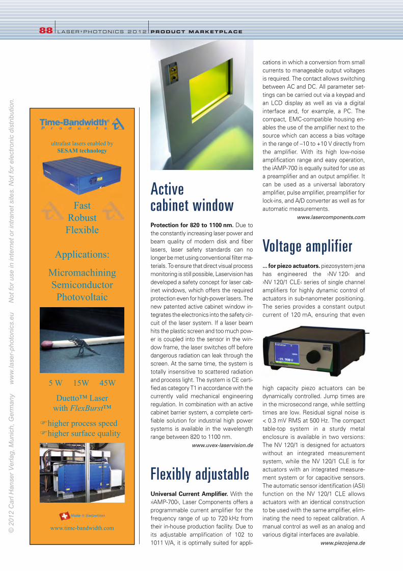
88 l LASER+PHOTONICS 2 0 12 lPRODUCT MARKETPLACE
Active cabinet window Protection for 820 to 1100 nm. Due to
the constantly increasing laser power and
beam quality of modern disk and fiber
lasers, laser safety standards can no
longer be met using conventional filter ma-
terials. To ensure that direct visual process
monitoring is still possible, Laservision has
developed a safety concept for laser cab-
inet windows, which offers the required
protection even for high-power lasers. The
new patented active cabinet window in-
tegrates the electronics into the safety cir-
cuit of the laser system. If a laser beam
hits the plastic screen and too much pow-
er is coupled into the sensor in the win-
dow frame, the laser switches off before
dangerous radiation can leak through the
screen. At the same time, the system is
totally insensitive to scattered radiation
and process light. The system is CE certi-
fied as category T1 in accordance with the
currently valid mechanical engineering
regulation. In combination with an active
cabinet barrier system, a complete certi-
fiable solution for industrial high power
systems is available in the wavelength
range between 820 to 1100 nm.
www.uvex-laservision.de
Flexibly adjustableUniversal Current Amplifier. With the
›iAMP-700‹, Laser Components offers a
programmable current amplifier for the
frequency range of up to 720 kHz from
their in-house production facility. Due to
its adjustable amplification of 102 to
1011 V/A, it is optimally suited for appli-
cations in which a conversion from small
currents to manageable output voltages
is required. The contact allows switching
between AC and DC. All parameter set-
tings can be carried out via a keypad and
an LCD display as well as via a digital
interface and, for example, a PC. The
compact, EMC-compatible housing en-
ables the use of the amplifier next to the
source which can access a bias voltage
in the range of –10 to +10 V directly from
the amplifier. With its high low-noise
amplification range and easy operation,
the iAMP-700 is equally suited for use as
a preamplifier and an output amplifier. It
can be used as a universal laboratory
amplifier, pulse amplifier, preamplifier for
lock-ins, and A/D converter as well as for
automatic measurements.
www.lasercomponents.com
Voltage amplifier ... for piezo actuators. piezosystem jena
has engineered the ›NV 120‹ and
›NV 120/1 CLE‹ series of single channel
amplifiers for highly dynamic control of
actuators in sub-nanometer positioning.
The series provides a constant output
current of 120 mA, ensuring that even
high capacity piezo actuators can be
dynamically controlled. Jump times are
in the microsecond range, while settling
times are low. Residual signal noise is
< 0.3 mV RMS at 500 Hz. The compact
table-top system in a sturdy metal
enclosure is available in two versions:
The NV 120/1 is designed for actuators
without an integrated measurement
system, while the NV 120/1 CLE is for
actuators with an integrated measure-
ment system or for capacitive sensors.
The automatic sensor identification (ASI)
function on the NV 120/1 CLE allows
actuators with an identical construction
to be used with the same amplifier, elim-
inating the need to repeat calibration. A
manual control as well as an analog and
various digital interfaces are available.
www.piezojena.de
88_produkte_LPex2012-x 15.12.2011 17:33 Uhr Seite 88
© 2
012
Car
l Han
ser V
erla
g, M
unic
h, G
erm
any
w
ww
.lase
r-ph
oton
ics.
eu
Not
for u
se in
inte
rnet
or i
ntra
net s
ites.
Not
for e
lect
roni
c di
strib
utio
n.
A. Laser beam sources
Oscillators, optical para-metric
GWU-LasertechnikPhone +49(0)2235 955220eMail [email protected] www.gwu-group.de/laser
Solid state lasers, diodepumped
www.gwu-group.de/laser
Solid state lasers, others
www.gwu-group.de/laser
C. Laser components
Crystals
www.gwu-group.de/laser
E. Electro-optics
Galvano-mirror systems
SCANLAB, www.scanlab.de
Modulators
IMT Masken und Teilungen AGGreifensee/SwitzerlandPhone +41(0)44 [email protected]
H. Raw materials
Crystals, non linear
GWU-LasertechnikPhone +49(0)2235 955220eMail [email protected] www.gwu-group.de/laser
Crystals, other
www.gwu-group.de/laser
Laser crystals
www.gwu-group.de/laser
I. Processed components
Components, optical,other
www.gwu-group.de/laser
IMT Masken und Teilungen AGGreifensee/SwitzerlandPhone +41(0)44 [email protected]
www.opticsbalzers.com
Grids, optical
IMT Masken und Teilungen AGGreifensee/SwitzerlandPhone +41(0)44 [email protected]
Prisms, optical
www.gwu-group.de/laser
Wave plates
www.gwu-group.de/laser
L. Optical production
Coatings, optical
IMT Masken und Teilungen AGGreifensee/SwitzerlandPhone +41(0)44 [email protected]
R. Laser materials processing, system Peripherals, Laser-assisted product development andconstruction
Photomask for laserapplications
IMT Masken und Teilungen AGGreifensee/SwitzerlandPhone +41(0)44 [email protected]
T. Optical metrology and testing technology, sensor technology
Autocollimators
www.moeller-wedel-optical.com
Interferometers
www.moeller-wedel-optical.com
Test systems for opticalcomponents
www.moeller-wedel-optical.com
TRADEDIRECTORYProducts – Technologies – Services
A. Laser-beam sources
B. Laser system components and radiation protection
C. Laser components
D. Opto-electronic components
E. Electro-optics
F. Acousto-optics
G. Display technology
H. Raw materials
I. Processed components
J. Optical systems
K. Opto-mechanics
L. Optical production
M. Services
N. Optical systems arranged by branch of industry
O. Optical transmission technology, fibre-optic technology
P. System integration
Q. System design – material design
R. Laser materials processing, system peripherals,
laser-assisted product development and construction
S. Holographic systems/accessoires
T. Optical measuring and testing technology, sensor technology
GROUPS
89_bqn_LPex12 15.12.2011 17:36 Uhr Seite 89
© 2
012
Car
l Han
ser V
erla
g, M
unic
h, G
erm
any
w
ww
.lase
r-ph
oton
ics.
eu
Not
for u
se in
inte
rnet
or i
ntra
net s
ites.
Not
for e
lect
roni
c di
strib
utio
n.
90 l LASER+PHOTONICS 2 0 12 l INDEX
AdlOptica 17
APE Angewandte Physik & Elektronik GmbH, Berlin 34, 81Arges GmbH, Wackersdorf 63, 69
asphericon 26
Basler 46
Baumer 47
Berliner Glas KGaA Herbert Kubatz GmbH & Co., Berlin 14Chemnitz University of
Technology 20
Chromasens 18
Cmosis 47, 64
Compotron GmbH, München 30, 49Constance University of
Applied Sciences 20
CSEM SA, Zürich/CH 16Dilas Diodenlaser GmbH, Mainz 11, 83
Docter Optics GmbH, Neustadt 15EdgeWave 84
EQ Photonics GmbH, Eching 64Expocentr Fairgrounds/Photonics 57Feinmess Dresden GmbH, Dresden 67, 69
Ficonet systems 17
Filtrop AG, Balzers/FL 46Fisba Optik AG, St. Gallen/CH 13Framos Electronic VertriebsGmbH, Pullach 32, 47
Frankfurt Laser Company (FLC) 82
Fraunhofer Institute for
Laser Technology (ILT) 84
Fresnel Optics GmbH, Apolda 12German Federal Ministry of
Economics and Technology 60
GWU-Lasertechnik Vertriebsges.mbH, Erftstadt 73H2BPhotonics 57
Hamamatsu Photonics Deutschland GmbH, Herrsching 27, 46
Hanser Verlag, München 41IDS 64
IMM Photonics GmbH, Unterschleißheim 69Ingeneric 4
InnoLight 76
Institute for Medical Laser
Technologies of Ulm University,
Germany 83
Instrument Systems GmbH,München 22, 44Jenoptik Lasers & Material
Processing 3, 53
Jenoptik Laser GmbH, Jena 31Jenoptik Optical Systems, Jena 3, 31, 53
Helmut Klingel GmbH, Pforzheim 65Laser 2000 65
Laser Components GmbH, Olching 59, 88
Laser Zentrum Hannover
(LZH) 3, 56
Laservision GmbH & Co.KG, Fürth 47, 88
Lasos Lasertechnik GmbH, Jena 81Layertec GmbH, Melingen 12Leistungselektronik Jena GmbH, Jena 42Leoni Fiber Optics GmbH,Neuhaus-Schierschnitz 17, 61Limo Lissotschenko Mikrooptik 83
Lower Saxony Ministry for
Economics, Technology and
Transport 56
m2k-laser 83
MAZeT GmbH, Jena 32MechOnics AG, München 42Menlo Systems 34
Messe Stuttgart/Lasys 55Micreon 57
Micro-Epsilon Messtechnik, Ortenburg 3, 35
Möller-Wedel Optical GmbH,Wedel 14Nanoplus GmbH, Gerbrunn 39,78
Nanoscribe 38
nanosystec 69
neoLASE 57
Newport Spectra Physics 3
Numerik Jena GmbH, Jena 74Omicron Laserage Laser-produkte GmbH, Rodgau 75Onefive GmbH, Zürich 34OptecNet Deutschland 60
Optenso Optical Engineering Software, Heerbrugg/CH 83
Optics Balzers AG, Balzers/FL 33, 51Optocraft GmbH, Erlangen 53Optotune 86
Optronis 65
OSA Optical Society of America/CLEO 79Owis GmbH, Staufen Titelseite, 37
Particular 57
PCO AG, Kelheim 5, 48
Phoenix Contact 65
Photonics West 60
Photonics21 53
Physik Instrumente GmbH & Co.KG, Karlsruhe 29, 38, 74PicoQuant 35
piezosystem jena 88
Polytec 35
Primes GmbH, Pfungstadt 82Qioptiq Photonics GmbH & Co.KG, Göttingen 16, 92Raylase AG, Wessling 62, 66
RGB Lasersysteme 34
Rofin 57, 84
Rofin-Lasag 70
Rowiak 57
Satisloh AG, Baar/CH 43Scanlab AG, Puchheim 7Schäfter + Kirchhoff GmbH, Hamburg 35, 82
Schott-Fostec 47
Schott AG, Mainz 8, 62Sill Optics 16
Sios Meßtechnik GmbH, Ilmenau 30SIS Stemmer Imaging ServicesGmbH, Puchheim 44, 64
SOLVing3D 48
Sony 64
Spectaris 60
Spectros AG, Ettingen/CH 71SPIE 60
SPIE/Photonics Europe 91Steinmeyer–Feinmess
Dresden 67, 69
SVS-Vistek GmbH, Seefeld 65, 81tec5 34
Tecnotion 69
Texas Instruments 64
Time-Bandwidth Products AG,Zürich/CH 88
Toptica Photonics AG, Gräfelfing 17, 82
Trioptics GmbH, Wedel 21Trumpf 84
Visiosens 47
Volpi 47
VRmagic 64
WZW Optic AG, Balgach/CH 45Xiton Photonics 83
Z-Laser Optoelektronik GmbH,Freiburg 46, 83
Carl Zeiss AG, Oberkochen 25Carl Zeiss 3, 16, 38, 55
Zett Optics 64
Zünd Präzisions-Optik AG,Diepoldsau/CH 51ZygoLOT 26
PERSONSArnold, Steffen 38
Axtner, Markus 66
Biertümpfel, Ralf 8
Blum, Mark 86
Du, Keming 84
Dürr, Ulrich 70
Fehn, Thomas 52
Flinn, Gregory 3, 52, 56
Freitag, Ingo 76
Glaschke, Torsten 26
Hambücker, Stefan 4
Haupt, Oliver 76
Hermatschweiler, Martin 38
Hildebrandt, Lars 78
Holst, Gerhard 48
Jedamzik, Ralf 8
Kiontke, Sven R. 26
Nähle, Lars 78
Rothweiler, Dirk 52
Rübenach, Olaf 4
Rüttimann, Christoph 70
Schnitzlein, Markus 18
Schwabedissen, Eric 22
Sinhoff, Volker 4
Spiekermann, Stefan 76
von Jan, Peter 66
Wessling, Christian 4
Witzleben, Alexander von 53
Wolf, Bernd-Michael 48
ADVERTISERS, COMPANIES AND INSTITUTIONS
■ Editor-in-ChiefDr. Gregory Flinn (responsible)
Kolbergerstrasse 22
81679 Munich, Germany
Tel. +49 89 99830-650
Fax +49 89 99830-623
■ EditorsLiane Thiele
Tel. +49 89 99830-612
■ PublisherCarl Hanser Verlag GmbH & Co. KG,
Kolbergerstrasse 22
81679 Munich, Germany
P.O. Box 86 04 20
81631 Munich, Germany
Tel. +49 89 99830-0
Fax +49 89 94809
www.hanser.de
■ Managing DirectorsWolfgang Beisler, Stephan D. Joss,
Michael Krüger
■ Advertisement ManagerMartin Ricchiuti (responsible)
Tel. +49 89 99830-686
Fax +49 89 99830-623
Miriam Weihe (Dispo)
Tel. +49 89 99830-216
Fax +49 89 99830-623
■ Layout and ProductionThomas West
Tel. +49 89 99830-422
Hadrian Zett (Production Manager)
Tel. +49 89 99830-420
■ PrintFirmengruppe APPL, sellier druck GmbH,
Angerstrasse 54
85354 Freising, Germany
Printed in Germany.
■ Copyright and Publishing RightsThe publication and all individual articles
and illustrations contained herein are
protected by copyright.
Upon an article being accepted for pub-
lication, the rights of publication, as well as
the rights of translation, of granting repro-
duction licences, of storage in electronic
retrieval systems, of producing special im-
pressions, photocopies and microcopies
are transferred to the publisher. Any utiliza-
tion thereof outside the limits of the copy-
right act is forbidden without the written
permission of the publisher.
■ Descriptive NamesThe use of general descriptive names, pro-
prietary names, trade names, commercial
designations or the like in this publication
in no way implies that such names may be
used freely: these are often legally protect-
ed, registered trademarks, even if not de-
signated as such.
While the advice and information in this
journal are believed to be true and accu-
rate at the date of its going to press,
neither the authors, the editors, nor the
publisher can accept any legal
responsibility for any errors or omissions
that may be made. The publisher makes
no warranty, express or implied, with
respect to the material contained herein.
© Carl Hanser Verlag, Munich 2012
90_LPX_Index_Impressum_fin 15.12.2011 17:42 Uhr Seite 90
© 2
012
Car
l Han
ser V
erla
g, M
unic
h, G
erm
any
w
ww
.lase
r-ph
oton
ics.
eu
Not
for u
se in
inte
rnet
or i
ntra
net s
ites.
Not
for e
lect
roni
c di
strib
utio
n.
Advances in applications of photonics, optics, lasers, and micro/nanotechnologies
Technologies- Micro/Nano Technologies
- Disruptive Organic and Bio Photonics
- Highly Integrated and Functional
Photonic Components
- Advances in Laser and
Amplifier Technologies
- Photonics in Industrial Applications
Conference dates16–20 April 2012
LocationThe Square Conference Centre
Brussels, Belgium
www.spie.org/aboutpe
Photonics2012
16-20 April 2012
Register Today
u3-u4_LPex2012 15.12.2011 17:49 Uhr Seite 1
© 2
012
Car
l Han
ser V
erla
g, M
unic
h, G
erm
any
w
ww
.lase
r-ph
oton
ics.
eu
Not
for u
se in
inte
rnet
or i
ntra
net s
ites.
Not
for e
lect
roni
c di
strib
utio
n.

The Sources for your Optical Solutions:LINOS Catalog & Online-Shop!
[email protected].: +49 (0) 551/ 6935-0www.qioptiq.com
SHOP
Detailed technical data for more than 4.800 standard products:
qioptiq-shop.com
Qis
Optical Power MonitorUSB powered and controlled Different detector heads 190 – 1600 nm available30 Hz update rate with GUI, 1000 Hz as data logger
O i l P M i
Lamphouse ILVersion for spectral lamps availableReproducible mechanical adjustment of lamp, mirror and collector
Light-tight
Spectrometer QwaveVIS version for 390 – 880 nm UV version for 200 – 400 nm NIR version for 750 – 950 nm Spectral resolution up to 0.2 nmExceptional thermal stabilityIncludes world‘s smartest spectroscopy software
Shearing InterferometerFor fast determination of laser collimation Three versions available for beam diameters between 1 mm – 25 mm Compatible with LINOS Micro-, Nanobench, and Tube C systems Robust and easy to use
Gold Plane Mirrors, Laser Quality
For the IR spectral range up to 25 μm Average reflection > 98 % (0° ≤ AOI ≤ 60°, unpolarized)Resistant against environmental influences due to dielectric protection layer
Please order your free copy of the LINOS Catalog 2012/13.Click: www.qioptiq-shop.com
Light-tight
Please ordthe LINOSClick: www
qi_11064_shop_anz_nov21.indd 1 28.11.11 10:04
u3-u4_LPex2012 15.12.2011 17:49 Uhr Seite 2
© 2
012
Car
l Han
ser V
erla
g, M
unic
h, G
erm
any
w
ww
.lase
r-ph
oton
ics.
eu
Not
for u
se in
inte
rnet
or i
ntra
net s
ites.
Not
for e
lect
roni
c di
strib
utio
n.