Embed Size (px)
Citation preview
Laser Directed Writing of Flat Lenses on Buckypaper
Journal: Nanoscale
Manuscript ID: NR-ART-04-2015-002481.R1
Article Type: Paper
Date Submitted by the Author: 19-May-2015
Complete List of Authors: Deng, Sunan; University of Birmingham, Penchev, Pavel; University of Birmingham, Liu, Jian; Sichuan University, Wang, Yongjing; University of Birmingham, Jiang, Kyle; University of Birmingham, Dimov, Stefan; University of Birmingham, Zhang, Zhichun; Harbin Institute of Technology, Liu, Yanju; Harbin Institute of Technology, Leng, Jinsong; Harbin Institute of Technology, Butt, Haider; University of Birmingham,
Nanoscale
Journal Name
ARTICLE
This journal is © The Royal Society of Chemistry 20xx J. Name., 2013, 00, 1-3 | 1
Please do not adjust margins
Please do not adjust margins
Received 00th January 20xx,
Accepted 00th January 20xx
DOI: 10.1039/x0xx00000x
www.rsc.org/
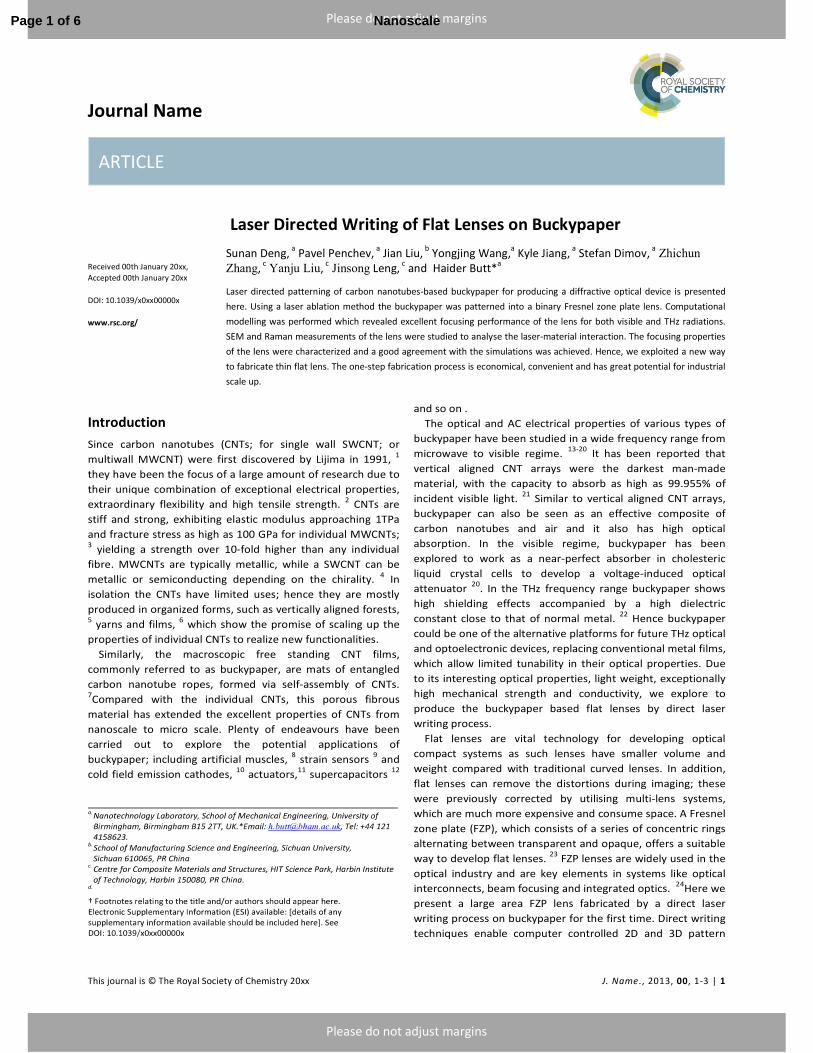
Laser Directed Writing of Flat Lenses on Buckypaper
Sunan Deng, a
Pavel Penchev, a
Jian Liu, b
Yongjing Wang,a Kyle Jiang,
a Stefan Dimov,
a Zhichun
Zhang, c Yanju Liu,
c Jinsong Leng,
c and Haider Butt*
a
Laser directed patterning of carbon nanotubes-based buckypaper for producing a diffractive optical device is presented
here. Using a laser ablation method the buckypaper was patterned into a binary Fresnel zone plate lens. Computational
modelling was performed which revealed excellent focusing performance of the lens for both visible and THz radiations.
SEM and Raman measurements of the lens were studied to analyse the laser-material interaction. The focusing properties
of the lens were characterized and a good agreement with the simulations was achieved. Hence, we exploited a new way
to fabricate thin flat lens. The one-step fabrication process is economical, convenient and has great potential for industrial
scale up.
Introduction
Since carbon nanotubes (CNTs; for single wall SWCNT; or
multiwall MWCNT) were first discovered by Lijima in 1991, 1
they have been the focus of a large amount of research due to
their unique combination of exceptional electrical properties,
extraordinary flexibility and high tensile strength. 2 CNTs are
stiff and strong, exhibiting elastic modulus approaching 1TPa
and fracture stress as high as 100 GPa for individual MWCNTs; 3 yielding a strength over 10-fold higher than any individual
fibre. MWCNTs are typically metallic, while a SWCNT can be
metallic or semiconducting depending on the chirality. 4 In
isolation the CNTs have limited uses; hence they are mostly
produced in organized forms, such as vertically aligned forests, 5 yarns and films,
6 which show the promise of scaling up the
properties of individual CNTs to realize new functionalities.
Similarly, the macroscopic free standing CNT films,
commonly referred to as buckypaper, are mats of entangled
carbon nanotube ropes, formed via self-assembly of CNTs. 7Compared with the individual CNTs, this porous fibrous
material has extended the excellent properties of CNTs from
nanoscale to micro scale. Plenty of endeavours have been
carried out to explore the potential applications of
buckypaper; including artificial muscles, 8 strain sensors
9 and
cold field emission cathodes, 10
actuators,11
supercapacitors 12
and so on .
The optical and AC electrical properties of various types of
buckypaper have been studied in a wide frequency range from
microwave to visible regime. 13-20
It has been reported that
vertical aligned CNT arrays were the darkest man-made
material, with the capacity to absorb as high as 99.955% of
incident visible light. 21
Similar to vertical aligned CNT arrays,
buckypaper can also be seen as an effective composite of
carbon nanotubes and air and it also has high optical
absorption. In the visible regime, buckypaper has been
explored to work as a near-perfect absorber in cholesteric
liquid crystal cells to develop a voltage-induced optical
attenuator 20
. In the THz frequency range buckypaper shows
high shielding effects accompanied by a high dielectric
constant close to that of normal metal. 22
Hence buckypaper
could be one of the alternative platforms for future THz optical
and optoelectronic devices, replacing conventional metal films,
which allow limited tunability in their optical properties. Due
to its interesting optical properties, light weight, exceptionally
high mechanical strength and conductivity, we explore to
produce the buckypaper based flat lenses by direct laser
writing process.
Flat lenses are vital technology for developing optical
compact systems as such lenses have smaller volume and
weight compared with traditional curved lenses. In addition,
flat lenses can remove the distortions during imaging; these
were previously corrected by utilising multi-lens systems,
which are much more expensive and consume space. A Fresnel
zone plate (FZP), which consists of a series of concentric rings
alternating between transparent and opaque, offers a suitable
way to develop flat lenses. 23
FZP lenses are widely used in the
optical industry and are key elements in systems like optical
interconnects, beam focusing and integrated optics. 24
Here we
present a large area FZP lens fabricated by a direct laser
writing process on buckypaper for the first time. Direct writing
techniques enable computer controlled 2D and 3D pattern
Page 1 of 6 Nanoscale
ARTICLE Journal Name
2 | J. Name., 2012, 00, 1-3 This journal is © The Royal Society of Chemistry 20xx
Please do not adjust margins
Please do not adjust margins
formation in a serial fashion. Compared with conventional
techniques like lithography, stamping, directed self-assembly,
or other patterning approaches that require masks or pre-
existing patterns, the laser direct writing process provides high
flexibility for arbitrary patterning via non-contact and maskless
fabrication process, which is much cheaper and convenient. 25
The study is of interest as it demonstrates the novel laser
processing of buckypaper for producing a working diffractive
optical device (FZP lens). The same method can also be applied
for patterning buckypaper for other applications.
The buckypaper FZP lens was fabricated on silicon substrate
with a radius of 2 mm and 16 Fresnel zones. A large area FZP
lens has great potential to be used in photovoltaic and imaging
applications. 26
SEM and Raman measurements are taken to
analyse CNTs after the laser process ablation. The working of
the FZP lens and its performance in the visible and terahertz
regimes was studied computationally. Experimental
measurements were also performed to characterize the lens in
the visible regime and good agreements with the simulations
were achieved.
Simulations
The FZP lens is designed according to this equation: ���
� ����
(n=1, 2, 3…), 27-29
where �� is the radius of the nth rings of a
FZP lens; f is the focal length; and λ is the wavelength of
incident light. In this work the central ring of the lens R1 is
500µm, and nmax=16.
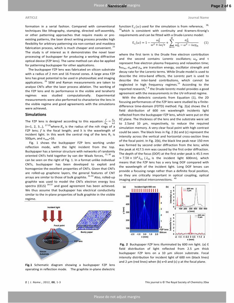
Fig. 1 shows the buckypaper FZP lens working under
reflection mode, with the light incident from the top.
Buckypaper has a laminar structure with networks of randomly
oriented CNTs held together by van der Waals forces, 12, 30
as
can be seen on the right of Fig. 1. In a format unlike individual
CNTs, buckypaper has been developed to exploit and
homogenize the excellent properties of CNTs. Given that CNTs
are rolled-up graphene layers, the general features of CNT
arrays are similar to those of bulk graphite. 31-33
Also, rolled-up
graphite was used to model the CNTs electron energy loss
spectra (EELS) 34-37
and good agreement has been achieved.
We thus assume that buckypaper has electrical conductivity
similar to the in-plane properties of bulk graphite in the visible
regime.
Fig.1 Schematic diagram showing a buckypaper FZP lens
operating in reflection mode. The graphite in-plane dielectric
function Ԑ�� used for the simulation is from reference, 38,
39which is consistent with continuity and Kramers-Kronig’s
requirements and can be fitted with a Drude-Lorenz model:
Ԑ�� � 1 � ���
�� � ��/� � � ���
��� � �� � ����
�
����1
where the first term is the Drude free electron contribution
and the second contains Lorentz oscillators; ω� and τ
represent free electron plasma frequency and relaxation time;
ħω� ,��and �� are transition energy, oscillator strength and
decay rate for the Lorentz terms. While Drude model is used to
describe the intra-band effects, the Lorentz part is used to
describe the inter-band contributions, which cannot be
neglected in high frequency regimes.13
According to the
reported research,7, 8
the Drude-lorentz model provides a good
agreement with the measurements in the UV-infrared regime.
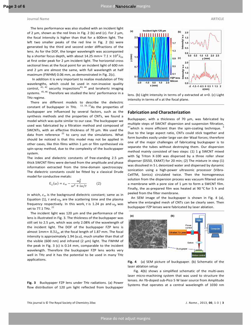
With the dielectric constants from Equation (1), the 2D
focusing performances of the FZP lens were studied by a finite-
difference time-domain (FDTD) method. Fig. 2(a) shows the E
field distribution of 600 nm wavelength incidents light
reflected from the buckypaper FZP lens, which were put on the
XZ plane. The thickness of the lens and the substrate were set
to 2.5and 10 µm, respectively, to reduce the required
simulation memory. A very clear focal point with high contrast
could be seen. The black lines in Fig. 2 (b) and (c) represent the
intensity across the vertical and horizontal cross-section lines
of the focal point. In Fig. 2(b), the black line peak near 150 mm
was formed by second order diffraction from the lens; while
the peak at 417.5 mm was caused by the first order diffraction.
The depth of the focus (DOF) at the first order peak is 45.5 mm
� 7.58 # 10%&'� ( &'� is the incident light 600nm), which
means that the FZP lens has a very long DOF compared with
the wavelength of the incident light. Long DOF lenses can
provide a focusing range rather than a definite focal position,
so they are critically important in optical coupling, optical
imaging and optical interconnections. 40
Fig. 2 Buckypaper FZP lens illuminated by 600 nm light. (a) E
field distribution of light reflected from 2.5 µm thick
buckypaper FZP lens on a 10 µm silicon substrate. Focal
intensity distribution for incident light of 600 nm (black lines)
and 2 µm (red lines) when (b) x=0 and (c) y at the focal plane.
Page 2 of 6Nanoscale
Journal Name ARTICLE
This journal is © The Royal Society of Chemistry 20xx J. Name., 2013, 00, 1-3 | 3
Please do not adjust margins
Please do not adjust margins
The lens performance was also studied with an incident light
of 2 µm, shown as the red lines in Fig. 2 (b) and (c). For 2 µm,
the focal intensity is higher than that for a 600nm light. The
left two smaller peaks of the red line in Fig. 2 (b) were
generated by the third and second order diffractions of the
lens. As for the DOF, the longer wavelength was accompanied
by a shorter focus depth, with about 14.25 mm� 7.1 # 10(&'�
at first order peak for 2 µm incident light. The horizontal cross
sectional lines at the focal point for an incident light of 600 nm
and 2 µm are almost the same, with full wavelength at half
maximum (FWHM) 0.06 mm, as demonstrated in Fig. 2(c).
In addition it is very important to realize modulation of THz
wavelengths, which could be used in non-invasive quality
control, 41, 42
security inspections43, 44
and terahertz imaging
systems. 45, 46
Therefore we studied the lens’ performance in a
THz regime.
There are different models to describe the dielectric
constant of buckypaper in THz. 13, 19, 22
As the properties of
buckypaper are influenced by several factors, such as the
synthesis methods and the properties of CNTs, we found a
model which was quite similar to our case. The buckypaper we
used was fabricated by a filtration method and composed of
SWCNTs, with an effective thickness of 70 µm. We used the
data from reference 22
to carry out the simulations. What
should be noticed is that this model may not be applied in
other cases, like thin films within 1 µm or film synthesised via
spin-spray method, due to the complexity of the buckcypaper
system.
The index and dielectric constants of free-standing 2.5 µm
thick SWCNT films were derived from the amplitude and phase
information extracted from the time-domain spectroscopy.
The dielectric constants could be fitted by a classical Drude
model for conductive metals:
Ԑ�� � )* � ���
�� � ��/��2
in which, )* is the background dielectric constant; same as in
Equation (1), � and �� are the scattering time and the plasma
frequency respectively. In this work, � is 1.24 ps and �� was
set to 77.1 THz. 22
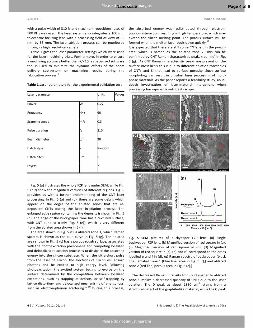
The incident light was 120 µm and the performance of the
lens is illustrated in Fig. 3. The thickness of the buckypaper was
still set to 2.5 µm, which was only 2.08% of the wavelength of
the incident light. The DOF of the buckypaper FZP lens is
almost 1mm� 8.3&'� at the focal length of 1.87 mm. The focal
intensity is approximately 1.94 (a.u), much smaller than that of
the visible (600 nm) and infrared (2 µm) light. The FWHM of
the peak in Fig. 3 (c) is 0.14 mm, comparable to the incident
wavelength. Therefore the buckypaper FZP lens works very
well in THz and it has the potential to be used in many THz
applications.
Fig. 3 Buckypaper FZP lens under THz radiations. (a) Power
flow distribution of 120 µm light reflected from buckypaper
lens. (b) Light intensity in terms of y extracted at x=0. (c) Light
intensity in terms of x at the focal plane.
Fabrication and Characterization
Buckypaper, with a thickness of 70 µm, was fabricated by
multiple steps of SWCNT dispersion and suspension filtration, 47
which is more efficient than the spin-coating technique. 3
Due to the large aspect ratio, CNTs could stick together and
form bundles easily under large van der Waal forces; therefore
one of the major challenges of fabricating buckypaper is to
separate the tubes without destroying them. Our dispersion
method mainly consisted of two steps: (1) 1 g SWCNT mixed
with 5g Triton X-100 was dispersed by a three roller shear
disperser (DS50, EXAKT) for 20 min; (2) The mixture in step (1)
was dissolved in 5 L deionized water and dispersed by dynamic
sonication using a high-power ultrasonic processor (Vibra-
CellTM, Sonics) circulated twice. Then the homogeneous
solution from the dispersion process was vacuum filtered onto
a membrane with a pore size of 1 µm to form a SWCNT film.
Finally, the as-prepared film was heated at 90 - for 5 h and
peeled from the filter membrane.
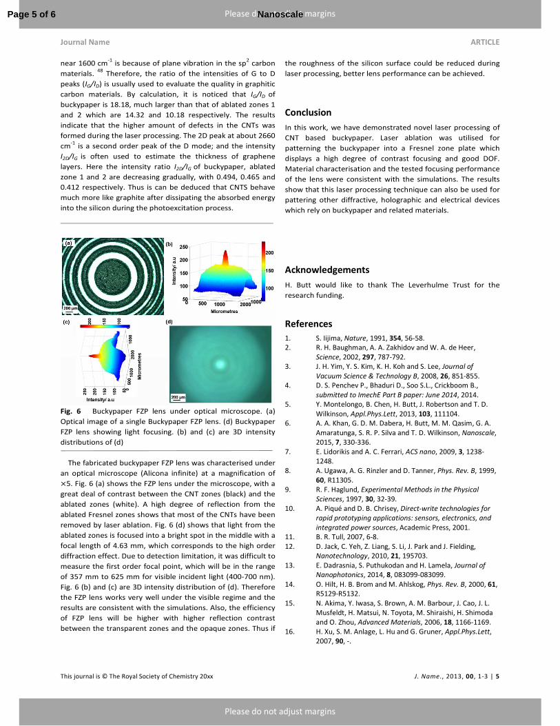
An SEM image of the buckypaper is shown in Fig. 4 (a),
where the entangled mesh of CNTs can be clearly seen. Then
buckypaper FZP lenses were fabricated by laser ablation.
Fig. 4 (a) SEM picture of buckypaper. (b) Schematic of the
laser ablation setup
Fig. 4(b) shows a simplified schematic of the multi-axes
laser micro-machining system that was used to structure the
lenses. An Yb-doped sub-Pico 5 W laser source from Amplitude
Systems that operates at a central wavelength of 1030 nm
Page 3 of 6 Nanoscale
ARTICLE Journal Name
4 | J. Name., 2012, 00, 1-3 This journal is © The Royal Society of Chemistry 20xx
Please do not adjust margins
Please do not adjust margins
with a pulse width of 310 fs and maximum repetitions rates of
500 KHz was used. The laser system also integrates a 100 mm
telecentric focusing lens with a processing field of view of 35
mm by 35 mm. The laser ablation process can be monitored
through a high resolution camera.
Table 1 gives the laser parameter settings which were used
for the laser machining trials. Furthermore, in order to ensure
a machining accuracy better than +/- 10, a specialized software
tool is used to minimize the dynamic effects of the beam
delivery sub-system on machining results during the
fabrication process.4
Table 1.Laser parameters for the experimental validation test
Laser parameter Units Values
Power
Frequency
W
kHz
0.27
60
Scanning speed m/s 0.3
Pulse duration fs 310
Beam diameter µm 30
Hatch style - Random
Hatch pitch µm 5
Layers - 7
Fig. 5 (a) illustrates the whole FZP lens under SEM, while Fig.
5 (b-f) show the magnified versions of different regions. Fig. 5
provides us with a further understanding of the CNT laser
processing. In Fig. 5 (a) and (b), there are some debris which
appear on the edges of the ablated zones that are re-
deposited CNTs during the laser irradiation process. The
enlarged edge region containing the deposits is shown in Fig. 5
(d). The edge of the buckypaper zone has a textured surface,
with CNT bundled trimly (Fig. 5 (e)); which is very different
from the ablated area shown in 5 (f).
The area shown in Fig. 5 (f) is ablated zone 1, which Raman
spectra is shown as the blue curve in Fig. 5 (g). The ablated
area shown in Fig. 5 (c) has a porous rough surface, associated
with the photoexcitation phenomena and competing localized
and delocalized relaxation processes to dissipate the absorbed
energy into the silicon substrate. When the ultra-short pulse
from the laser hit silicon, the electrons of Silicon will absorb
photons and be excited to high energy level. Following
photoexcitation, the excited system begins to evolve on the
surface determined by the competition between localized
excitations- such as trapping at defects, or self-trapping by
lattice distortion- and delocalized mechanisms of energy loss,
such as electron-phonon scattering.9, 10
During this process,
the absorbed energy was redistributed through electron-
phonon interaction, resulting in high temperature, which may
exceed the silicon melting point. The porous surface will be
formed when the molten layer cools down quickly.11
It is expected that there are still some CNTs left in the porous
area, which is named as the ablated zone 2. This can be
confirmed by CNT Raman characteristic peaks (red line) in Fig.
5 (g). As CNT Raman characteristic peaks are present on the
surface most likely this is due to different ablation thresholds
of CNTs and Si that lead to surface porosity. Such surface
morphology can result in ultrafast laser processing of multi-
phase materials. As the paper reports a feasibility study, an in-
depth investigation of laser-material interactions when
processing buckypaper is outside its scope.
Fig. 5 SEM pictures of buckypaper FZP lens. (a) Single
buckypaper FZP lens. (b) Magnified version of red square in (a).
(c) Magnified version of red square in (b). (d) Magnified
version of red square in (c). (e) and (f) correspond to the areas
labelled e and f in (d). (g) Raman spectra of buckypaper (black
line), ablated zone 1 (blue line, area in Fig. 5 (f),) and ablated
zone 2 (red line, porous area in Fig. 5 (c),)
The decreased Raman intensity from buckypaper to ablated
zone 2 implies a decreased quantity of CNTs due to the laser
ablation. The D peak at about 1330 cm-1
stems from a
structural defect of the graphite-like material, while the G peak
Page 4 of 6Nanoscale
Journal Name ARTICLE
This journal is © The Royal Society of Chemistry 20xx J. Name., 2013, 00, 1-3 | 5
Please do not adjust margins
Please do not adjust margins
near 1600 cm-1
is because of plane vibration in the sp2 carbon
materials. 48
Therefore, the ratio of the intensities of G to D
peaks (IG/ID) is usually used to evaluate the quality in graphitic
carbon materials. By calculation, it is noticed that IG/ID of
buckypaper is 18.18, much larger than that of ablated zones 1
and 2 which are 14.32 and 10.18 respectively. The results
indicate that the higher amount of defects in the CNTs was
formed during the laser processing. The 2D peak at about 2660
cm-1
is a second order peak of the D mode; and the intensity
I2D/IG is often used to estimate the thickness of graphene
layers. Here the intensity ratio I2D/IG of buckypaper, ablated
zone 1 and 2 are decreasing gradually, with 0.494, 0.465 and
0.412 respectively. Thus is can be deduced that CNTS behave
much more like graphite after dissipating the absorbed energy
into the silicon during the photoexcitation process.
Fig. 6 Buckypaper FZP lens under optical microscope. (a)
Optical image of a single Buckypaper FZP lens. (d) Buckypaper
FZP lens showing light focusing. (b) and (c) are 3D intensity
distributions of (d)
The fabricated buckypaper FZP lens was characterised under
an optical microscope (Alicona infinite) at a magnification of
#5. Fig. 6 (a) shows the FZP lens under the microscope, with a
great deal of contrast between the CNT zones (black) and the
ablated zones (white). A high degree of reflection from the
ablated Fresnel zones shows that most of the CNTs have been
removed by laser ablation. Fig. 6 (d) shows that light from the
ablated zones is focused into a bright spot in the middle with a
focal length of 4.63 mm, which corresponds to the high order
diffraction effect. Due to detection limitation, it was difficult to
measure the first order focal point, which will be in the range
of 357 mm to 625 mm for visible incident light (400-700 nm).
Fig. 6 (b) and (c) are 3D intensity distribution of (d). Therefore
the FZP lens works very well under the visible regime and the
results are consistent with the simulations. Also, the efficiency
of FZP lens will be higher with higher reflection contrast
between the transparent zones and the opaque zones. Thus if
the roughness of the silicon surface could be reduced during
laser processing, better lens performance can be achieved.
Conclusion
In this work, we have demonstrated novel laser processing of
CNT based buckypaper. Laser ablation was utilised for
patterning the buckypaper into a Fresnel zone plate which
displays a high degree of contrast focusing and good DOF.
Material characterisation and the tested focusing performance
of the lens were consistent with the simulations. The results
show that this laser processing technique can also be used for
pattering other diffractive, holographic and electrical devices
which rely on buckypaper and related materials.
Acknowledgements
H. Butt would like to thank The Leverhulme Trust for the
research funding.
References
1. S. Iijima, Nature, 1991, 354, 56-58.
2. R. H. Baughman, A. A. Zakhidov and W. A. de Heer,
Science, 2002, 297, 787-792.
3. J. H. Yim, Y. S. Kim, K. H. Koh and S. Lee, Journal of
Vacuum Science & Technology B, 2008, 26, 851-855.
4. D. S. Penchev P., Bhaduri D., Soo S.L., Crickboom B.,
submitted to ImechE Part B paper: June 2014, 2014.
5. Y. Montelongo, B. Chen, H. Butt, J. Robertson and T. D.
Wilkinson, Appl.Phys.Lett, 2013, 103, 111104.
6. A. A. Khan, G. D. M. Dabera, H. Butt, M. M. Qasim, G. A.
Amaratunga, S. R. P. Silva and T. D. Wilkinson, Nanoscale,
2015, 7, 330-336.
7. E. Lidorikis and A. C. Ferrari, ACS nano, 2009, 3, 1238-
1248.
8. A. Ugawa, A. G. Rinzler and D. Tanner, Phys. Rev. B, 1999,
60, R11305.
9. R. F. Haglund, Experimental Methods in the Physical
Sciences, 1997, 30, 32-39.
10. A. Piqué and D. B. Chrisey, Direct-write technologies for
rapid prototyping applications: sensors, electronics, and
integrated power sources, Academic Press, 2001.
11. B. R. Tull, 2007, 6-8.
12. D. Jack, C. Yeh, Z. Liang, S. Li, J. Park and J. Fielding,
Nanotechnology, 2010, 21, 195703.
13. E. Dadrasnia, S. Puthukodan and H. Lamela, Journal of
Nanophotonics, 2014, 8, 083099-083099.
14. O. Hilt, H. B. Brom and M. Ahlskog, Phys. Rev. B, 2000, 61,
R5129-R5132.
15. N. Akima, Y. Iwasa, S. Brown, A. M. Barbour, J. Cao, J. L.
Musfeldt, H. Matsui, N. Toyota, M. Shiraishi, H. Shimoda
and O. Zhou, Advanced Materials, 2006, 18, 1166-1169.
16. H. Xu, S. M. Anlage, L. Hu and G. Gruner, Appl.Phys.Lett,
2007, 90, -.
Page 5 of 6 Nanoscale
ARTICLE Journal Name
6 | J. Name., 2012, 00, 1-3 This journal is © The Royal Society of Chemistry 20xx
Please do not adjust margins
Please do not adjust margins
17. T. Kampfrath, K. von Volkmann, C. Aguirre, P. Desjardins,
R. Martel, M. Krenz, C. Frischkorn, M. Wolf and L. Perfetti,
Physical review letters, 2008, 101, 267403.
18. Q. Zhang, E. H. Hároz, Z. Jin, L. Ren, X. Wang, R. S.
Arvidson, A. Lüttge and J. Kono, Nano Lett., 2013, 13,
5991-5996.
19. T.-I. Jeon, K.-J. Kim, C. Kang, S.-J. Oh, J.-H. Son, K. H. An, D.
J. Bae and Y. H. Lee, Appl.Phys.Lett, 2002, 80, 3403-3405.
20. H.-K. Ma, P.-C. Chien, M.-C. Tsai, H.-Y. Miao, J.-H. Liu and
C.-Y. Huang, Optical Materials Express, 2014, 4, 719-724.
21. Z.-P. Yang, L. Ci, J. A. Bur, S.-Y. Lin and P. M. Ajayan, Nano
Lett., 2008, 8, 446-451.
22. J. Hong, D. J. Park, J. H. Yim, J. Park, J.-Y. Park, S. Lee and Y.
Ahn, The Journal of Physical Chemistry Letters, 2013, 4,
3950-3957.
23. K. Rastani, A. Marrakchi, S. F. Habiby, W. M. Hubbard, H.
Gilchrist and R. E. Nahory, Appl.Optics, 1991, 30, 1347-
1354.
24. H. Butt, R. Rajesekharan, Q. Dai, S. Sarfraz, R. V. Kumar, G.
A. Amaratunga and T. D. Wilkinson, Appl.Phys.Lett, 2012,
101, 243116.
25. W. Xiong, Y. S. Zhou, W. J. Hou, L. J. Jiang, Y. Gao, L. S. Fan,
L. Jiang, J. F. Silvain and Y. F. Lu, Scientific reports, 2014, 4.
26. W. T. Xie, Y. J. Dai, R. Z. Wang and K. Sumathy, Renewable
and Sustainable Energy Reviews, 2011, 15, 2588-2606.
27. R. Ranjith, H. Butt, T. Wilkinson and G. Amaratunga,
Advanced Materials, 2012, 24, OP170-OP173.
28. S. Deng, A. K. Yetisen, K. Jiang and H. Butt, RSC.Adv., 2014,
4, 30050-30058.
29. X.-T. Kong, A. A. Khan, P. R. Kidambi, S. Deng, A. K. Yetisen,
B. Dlubak, P. Hiralal, Y. Montelongo, J. Bowen and S.
Xavier, ACS Photonics, 2014.
30. S. Roy, V. Jain, R. Bajpai, P. Ghosh, A. Pente, B. Singh and
D. Misra, The Journal of Physical Chemistry C, 2012, 116,
19025-19031.
31. Y. Murakami, E. Einarsson, T. Edamura and S. Maruyama,
Physical Review Letters, 2005, 94, 087402.
32. M. F. Lin, F. L. Shyu and R. B. Chen, Phys. Rev. B, 2000, 61,
14114-14118.
33. H. Pan, Y. Feng and J. Lin, Phys. Rev. B, 2005, 72, 085415.
34. A. Seepujak, U. Bangert, A. Harvey, P. Costa and M. Green,
Phys. Rev. B, 2006, 74, 075402.
35. O. Stéphan, D. Taverna, M. Kociak, K. Suenaga, L. Henrard
and C. Colliex, Phys. Rev. B, 2002, 66, 155422.
36. A. Rivacoba and F. J. García de Abajo, Phys. Rev. B, 2003,
67, 085414.
37. M. Kociak, L. Henrard, O. Stéphan, K. Suenaga and C.
Colliex, Phys. Rev. B, 2000, 61, 13936-13944.
38. H. Butt, Q. Dai, R. Rajesekharan, T. D. Wilkinson and G. A.
Amaratunga, ACS nano, 2011, 5, 9138-9143.
39. T. D. W. H. Butt, G.A.J. Amaratunga, Progress in
Electromagnetics Research, 2012, M,22, 1-12.
40. X.-Y. Jiang, J.-S. Ye, J.-W. He, X.-K. Wang, D. Hu, S.-F. Feng,
Q. Kan and Y. Zhang, Opt. Express, 2013, 21, 30030-30038.
41. H. Hoshina, Y. Sasaki, A. Hayashi, C. Otani and K. Kawase,
Applied spectroscopy, 2009, 63, 81-86.
42. F. Rutz, M. Koch, S. Khare, M. Moneke, H. Richter and U.
Ewert, International journal of infrared and millimeter
waves, 2006, 27, 547-556.
43. K. Yamamoto, M. Yamaguchi, F. Miyamaru, M. Tani, M.
Hangyo, T. Ikeda, A. Matsushita, K. Koide, M. Tatsuno and
Y. Minami, Japanese journal of applied physics, 2004, 43,
L414.
44. M. C. Kemp, P. Taday, B. E. Cole, J. Cluff, A. J. Fitzgerald
and W. R. Tribe, 2003.
45. K. J. Siebert, T. Löffler, H. Quast, M. Thomson, T. Bauer, R.
Leonhardt, S. Czasch and H. G. Roskos, Physics in medicine
and biology, 2002, 47, 3743.
46. A. W. Lee and Q. Hu, Opt.Lett, 2005, 30, 2563-2565.
47. H. Chu, Z. Zhang, Y. Liu and J. Leng, Carbon, 2014, 66, 154-
163.
48. J. Li, X. Cheng, J. Sun, C. Brand, A. Shashurin, M. Reeves
and M. Keidar, Journal of Applied Physics, 2014, 115,
164301.
Page 6 of 6Nanoscale