Embed Size (px)
Citation preview
BULLETIN OF THE POLISH ACADEMY OF SCIENCES
TECHNICAL SCIENCES
Vol. 56, No. 1, 2008
Laser Direct Imaging of tracks on PCB covered with laser
photoresist
R. BARBUCHA1∗, M. KOCIK1, J. MIZERACZYK1,2, G. KOZIOŁ3, and J. BORECKI3
1 Centre for Plasma and Laser Engineering, The Szewalski Institute of Fluid Flow Machinery,
Polish Academy of Sciences, 14 Fiszera St., 80-231 Gdańsk, Poland2 Department of Marine Electronics, Gdynia Maritime University,
83 Morska St., 81-225 Gdynia, Poland3 Advanced Printed Circuit Board Technologies, Tele & Radio Research Institute,
11 Ratuszowa St., 03-450, Warsaw, Poland
Abstract. The increasing demands for miniaturization and better functionality of electronic components and devices have a significant effect
on the requirements facing the printed circuit board (PCB) industry. PCB manufactures are driving for producing high density interconnect
(HDI) boards at significantly reduced cost and reduced implementation time. The interconnection complexity of the PCB is still growing
and today calls for 50/50 µm or 25/25 µm technology are real. Existing technologies are unable to offer acceptable solution. Recently the
Laser Direct Imaging (LDI) technology is considered as an answer for these challenges. LDI is a process of imaging electric circuits directly
on PCB without the use of a phototool or mask. Our laboratory system for Laser Direct Imaging is designed for tracks and spaces on PCB
with minimum width distance of 50/50 µm. In comparison with conventional photolithography method, this technology is much better for
50/50 µm track and spaces. In our research we used photoresist with resolution 50 µm, but in case of using laser photoresists with better
resolution (e.g. 25 µm) it will be possible to image tracks in super-fine-line technology (25/25 µm). The comparison between two technology
of creating mosaic pattern tracks on PCB proved that laser imaging is promising technology in high density interconnects patterns, which
are widely use in multilayered PCB and similar applications.
Key words: Laser Direct Imaging (LDI), photoresist, printed circuit board (PCB), UV laser.
1. Introduction
Since many years electronics market calls for smaller and
lighter and more reliable portable electronic devices. As chal-
lenges facing to electronic devices manufactures are going to
be more critical, they create new, smaller housings of the inte-
grated circuits. As a result, there are new, alternative designs
of the multioutput circuits named CSP (Chip Scale Package).
This construction leads to decreasing of induction and delay
time of signal propagation as well as decreasing electromag-
netic noise. There are new trends in this area:
• creating circuits housings with taped electric outputs situ-
ated on each four side with very small raster <0.5 mm,
• turning wire outputs into spherical contacts,
• turning the housings with outputs situated on its circum-
ference into outputs situated at the whole bottom side as a
net with very small raster,
• integrating a bared semiconductor structures directly on
PCB using “flip-chip” technology.
Existing technologies are unable to offer acceptable solu-
tion and the inevitable results is reduced production efficiency
and lower yields. For example, a R/C devices manufactures
creates from year to year a smaller components such as 0402
(1 × 0.5 mm) or 0201 (0.5 × 0.25 mm) or 01005 (0.5 ×
0.25 mm). During last five years an average tracks width in
conventional PCB’s reduced from 200 µm to 100 µm. Dur-
ing next five years, the tracks width will reach 75 µm. So,
conventional PCB’s will be manufactured in HDI (High Den-
sity Interconnects) technology where tracks and spaces of the
electric circuits on PCB is 75/75 µm with 20 pads per cm2
or even 50/50 µm in new technology fabrics.
Recently, major number of the PCB manufactures pro-
duces circuits board using masks to create circuits pattern
on the photoresist (photochemical process). This technology
unfortunately reached its limits due to creating high density
interconnects on PCB. It is unable to create fine track on PCB
below 150 µm of track width and spaces. This is a result of
dramatically increasing number of losses.
Several new technologies have been developed and utilized
in recent years to address this challenge. One particular solu-
tion based on the Laser Direct Imaging (LDI) has managed
to prove itself, as the best and most comprehensive imaging
solution for HDI boards [1]. LDI uses focused laser beam to
direct expose PCB panel coated by photoresist, eliminating
the use of phototools and exposure systems and avoiding all
inherent problems, such as [2]:
• repeat defects from phototool handling and off-contact ex-
posure,
• poor dimensional stability of the phototools (changes of
size with temperature and humidity),
∗e-mail: [email protected]
17

R. Barbucha, M. Kocik, J. Mizeraczyk, G. Kozioł and J. Borecki
• material changes of each panel between panels of the same
batch.
LDI is carried out using a laser beam that is scanned
across photoresist surface and switched on and off by means
of a computer control system according to the electrical cir-
cuit pattern. It has been proved that LDI systems, which work
in UV spectrum are most suitable for obtaining fine lines and
spaces below 50 µm [1]. In order to be used in HDI board
production, an LDI system should have the following capa-
bilities [3]:
• high quality exposure of fine lines and spaces down to at
least 50 microns and below if possible,
• good depth of focus ensuring imaging quality for high to-
pography design. This is especially needed for uniform ex-
posure of outer layers and Sequential Build Up applications
(SBU),
• a system design that can accommodate various product
types, materials, thicknesses, manufacturing technologies
and production steps,
• a flexible, highly accurate registration system compatible
with different manufacturing technologies and production
steps,
• an ability to compensate dynamically for material dimen-
sion changes in order to overcome variance in panels form
the same batch and to be able to achieve tight registration
tolerance over the whole area of PCB panels.
The major advantage of LDI technology can be observed
in reduced steps in imaging conductive pattern on PCB, par-
ticularly using of the masks. Table 1 shows differences be-
tween conventional and LDI technology.
Table 1
Steps in conventional and laser method of creating conductive pattern on
PCB
Conventional Method LDI Method
Preparing computer data
for imaging masks
Preparing computer data
laser imaging
Imaging MasksPreparing a Copper
surface of PCB
Development of masks Lamination of the photoresist
Conditioning of masksLaser Direct Imaging
with LDI system
Preparing a Copper surface of PCB
Lamination of the photoresist
Fitting masks on PCB
and creating vacuum
UV imaging in UV curing machine
2. Experimental setup
Our system consists of three major components: the UV diode
laser (λ = 375 nm), the telescope and the optical scanner
XY (Fig. 1). The UV diode laser generates a laser beam at
average output power of 9 mW. The optical scanner has built-
in two high speed galvo drivers with mirrors, which allows
to displace focused laser beam with maximum velocity of 1
m/s. The scanner head is connected to a computer through
a PC card. To focus the laser beam, the F-Theta objective
(f = 100 mm) is used. The working area of the scanner head
is 6 cm × 6 cm. A computer controlled telescope can dy-
namically change the laser beam divergence, which allows to
change a laser spot size over the working area of the scanner.
A control program was developed to run the scanner head
(X-Y) and the telescope (Z) according to the patterns consist-
ed of tracks with different widths. This program operates on
HPGL files, which are widely used in the commercial devices
related with PCB industry. System for Laser Direct Imaging
in presented version is equipped with stationary table, which
could be leveled in two dimensions to obtain an ideal distance
between imaged PCB and focusing lens. This is necessary for
imaging fine thin tracks in all working area of optical scan-
ner. The final tracks width can be also adjusted by one of the
motorized telescope lens, which has ring with a scale. Those
adjustment elements are used for system calibration.
Fig. 1. Scheme of LDI system connections after Ref.4
The computer program has implemented two basic shape
generators: multi-line generator and rectangle generator. Each
generator can operate in two modes: “wobble” and “line by
line”. The wobble mode is used to obtaining tracks with
widths larger than the laser spot size. This is realized by join-
ing two movements: linear movement along the specified vec-
tor and circular movement added to the linear. Changing the
frequency and amplitude of circular movement one can ob-
tain different tracks widths. This mode can be used only for
tracks widths higher than 100 µm due to minimal amplitude
of circular movement.
Second mode “line by line” can generate wide lines, which
are combined with adherent lines. This method of imaging
lines can be performed without any spaces between lines or
with lines overlapping method. The degree of overlapping can
be adjusted to obtain an optimum laser power distribution over
the line surface.
At the moment, presented system for LDI allows to work
in two dimensional area only. In the future a flat table will be
changed to movable XYZ table, which expand all system ca-
pabilities. It will be possible to manufacture three dimensional
shapes or elements made from special dry photoresists, which
cure upon influence of UV laser beam radiation. 3D figures
will be imaged layer by layer with micrometer resolution. This
technique is suitable for small elements prototyping and can
be used e.g. in medicine. In Fig. 2 a view of our laboratory
system for LDI in present state is presented.
18 Bull. Pol. Ac.: Tech. 56(1) 2008
Laser Direct Imaging of tracks on PCB covered with laser photoresist
Fig. 2. A view of a real laboratory system for LDI
3. Results
During experiments of laser direct imaging on conven-
tional photoresist KOLON, which photosensivity was 35–
50 mJ/cm2, we put a major impact on imaging tracks 50/50
µm. Tests were carried out on conventional photoresist to
prove, that widely used conventional photoresist is suitable
for LDI technology. The use of conventional phoresist is im-
portant for PCB manufactures, since the new LDI technology
should be compatible to PCB’s production process. During
tests the velocity of imaging, frequency and, amplitude of cir-
cular movement, overlapping of the adherent lines and also
average power of a laser beam were changed and optimal pa-
rameters for each operating modes of LDI system were found.
Fig. 3. Test pattern consisted of lines with different widths and angles and
also circles inside
In Fig. 3 a standard test consisted of parallel lines with dif-
ferent widths around a central circular pattern are presented.
The test was prepared to answer for the following problems:
• how the line width is dependent on angle of imaging,
• what is a quality of tracks when track widths and spaces
are equal,
• what is a quality of tracks when spaces between tracks are
two times wider than tracks widths.
The test shows also the quality of imaging of circles and
track’s angles. The experiments resulted in obtaining exact
values of imaging process parameters. Imaging speed, was
found to be optimal at 5 cm/s. Imaging with this speed pro-
duces fine tracks with smooth surface of photoresist lines
without any irregulars at the track edges. Imaging with slow-
er speed leads to much more irregular, rugged surface of line
surface, which also resulted in bad edges. On the other hand,
imaging with higher speed causes washing away of the tracks
during development process, due to much smaller energy of
laser radiation delivered to the photoresist surface.
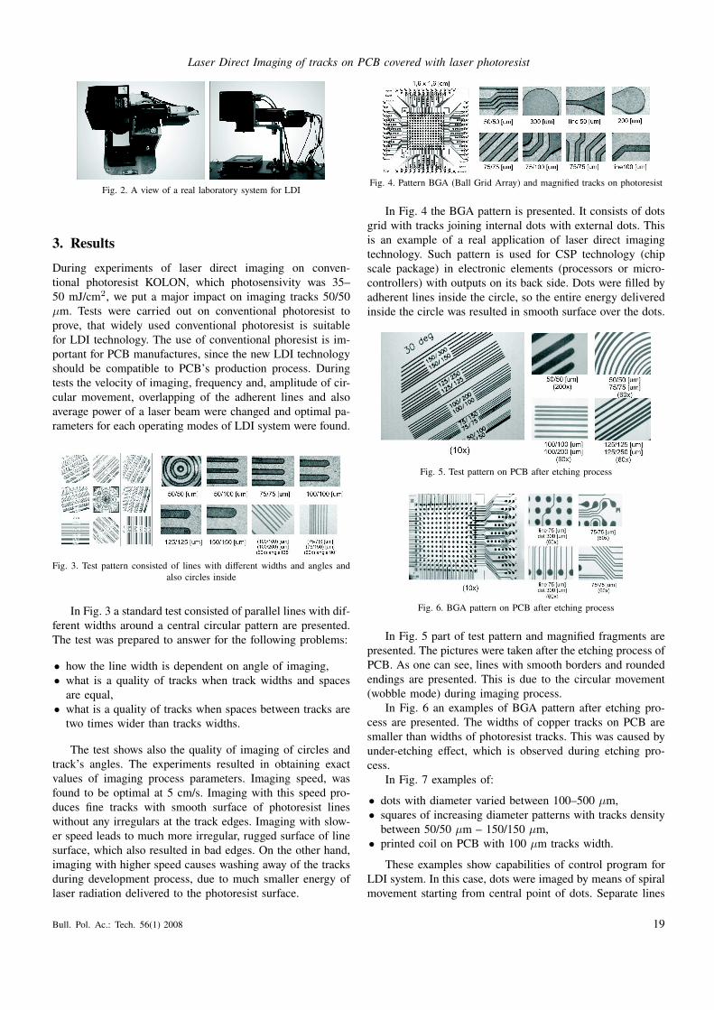
Fig. 4. Pattern BGA (Ball Grid Array) and magnified tracks on photoresist
In Fig. 4 the BGA pattern is presented. It consists of dots
grid with tracks joining internal dots with external dots. This
is an example of a real application of laser direct imaging
technology. Such pattern is used for CSP technology (chip
scale package) in electronic elements (processors or micro-
controllers) with outputs on its back side. Dots were filled by
adherent lines inside the circle, so the entire energy delivered
inside the circle was resulted in smooth surface over the dots.
Fig. 5. Test pattern on PCB after etching process
Fig. 6. BGA pattern on PCB after etching process
In Fig. 5 part of test pattern and magnified fragments are
presented. The pictures were taken after the etching process of
PCB. As one can see, lines with smooth borders and rounded
endings are presented. This is due to the circular movement
(wobble mode) during imaging process.
In Fig. 6 an examples of BGA pattern after etching pro-
cess are presented. The widths of copper tracks on PCB are
smaller than widths of photoresist tracks. This was caused by
under-etching effect, which is observed during etching pro-
cess.
In Fig. 7 examples of:
• dots with diameter varied between 100–500 µm,
• squares of increasing diameter patterns with tracks density
between 50/50 µm – 150/150 µm,
• printed coil on PCB with 100 µm tracks width.
These examples show capabilities of control program for
LDI system. In this case, dots were imaged by means of spiral
movement starting from central point of dots. Separate lines
Bull. Pol. Ac.: Tech. 56(1) 2008 19

R. Barbucha, M. Kocik, J. Mizeraczyk, G. Kozioł and J. Borecki
in increasing square patterns (multi-square patterns) were im-
aged using “line by line” method. The coil printed on PCB
was imaged using “wobble” method.
Fig. 7. Examples of different patterns on PCB, which show capabilities of
control program for LDI system
In Fig. 8 four examples of tracks mosaic on PCB are pre-
sented. These examples were prepared using another function
of control program – imaging from bitmap. These examples
were published over the internet in PDF (Portable Data File)
files, so the initial conversion into bitmap (BMP) file format
was performed. This method of imaging tracks on PCB con-
sist in separate imaging each pixel of the bitmap file. Using
the presented system it is possible to obtain density of inter-
connects at 100/100 µm.
Fig. 8. Examples of bitmap imaging method of LDI system
4. Conclusions
Our recent results of the laser direct imaging using laborato-
ry system for LDI proved that this technology is promising
solution for high density patterns of the circuits on PCB. We
obtained good results in imaging of the PCB covered by con-
ventional photoresist which UV-sensitivity was 55 mJ/cm2.
We obtained 50/50 µm tracks and spaces density on photore-
sist layer, therefore the presented system can be suitable for
super fine line technology. To check various shapes which can
be present in a real PCB patterns we have developed a special
test patterns: “Lines” and “BGA”.
When portable equipment becomes more powerfull also
complexity of the tracks on PCB is growing. The newest trend
in PCB manufacturing is multilayered PCB’s where even 100
layers can be developed. This multilayered technology is used
today in computer motherboards. This allows to simplify all
architecture of connections on motherboard PCB which has a
significant impact on reduced overall costs. This is one of the
solutions for high densities of interconnects and CSP tech-
nologies.
At now, our system for LDI is designed for imaging of
the circuitry patterns on PCB covered by photoresist on area
6 × 6 cm, but we plan to wide up this area using a com-
puter controlled XY table. It will allow to turn this system
into a commercial system, where computer motherboard size
PCB’s are manufactured. This system can be also adapted as
a system for stereo lithography in liquid photoresists. This
improvement will allow to produce shapes with high preci-
sion and resolution of the elements. It will find application
in medicine and other related fields where high precision and
complexity of shapes are required.
Acknowledgements. This research was supported by Re-
search Project nr 3T11B02027 of Ministry of Science and
Higher Education.
REFERENCES
[1] A. Sullau and A. Wiemers, Laser Direct Imaging, ILFA Pub-
lication, Hannover, 1999.
[2] B. Barclay, M. Morrell, “Laser Direct Imaging – A user per-
spective”, Leiterplatten Magazine 7–8, 1–11 (2001).
[3] Udi Omer, “Laser direct imaging – a comprehensive imaging
solution for HDI, TPCA Show, (2001).
[4] www.scanlab.de.
[5] K.H. Dietz and M.R. McKeever, “Development of high speed
UV-Laser Direct Imaging dry film photoresists”, Proc. S12-1,
IPC Printed Circuits Expo and Technical Conf., on CD (2000).
[6] Udi Omer, “An introduction to laser direct imaging for high
density interconnects”, Circuit World 29(1), 32–35 (2002).
[7] R. Barbucha, M. Kocik, J. Mizeraczyk, G. Kozioł, and J. Bo-
recki, “Laboratory system for Laser Direct Imaging”, Electron-
ics, 35–37 (2006), (in Polish).
[8] R. Barbucha, M. Kocik, J. Mizeraczyk, G. Kozioł, and J. Bo-
recki, “Laser imaging of tracks mosaic on Printed Circuit
Boards”, IV State Electronics Conf., 579–584 (2005), (in Pol-
ish).
20 Bull. Pol. Ac.: Tech. 56(1) 2008